EP1929348B1 - Stapelbare spleiss-chip-einrichtung - Google Patents
Stapelbare spleiss-chip-einrichtung Download PDFInfo
- Publication number
- EP1929348B1 EP1929348B1 EP06802138A EP06802138A EP1929348B1 EP 1929348 B1 EP1929348 B1 EP 1929348B1 EP 06802138 A EP06802138 A EP 06802138A EP 06802138 A EP06802138 A EP 06802138A EP 1929348 B1 EP1929348 B1 EP 1929348B1
- Authority
- EP
- European Patent Office
- Prior art keywords
- splice
- chip
- tray
- splice chip
- chips
- Prior art date
- Legal status (The legal status is an assumption and is not a legal conclusion. Google has not performed a legal analysis and makes no representation as to the accuracy of the status listed.)
- Not-in-force
Links
- 238000003860 storage Methods 0.000 claims description 9
- 238000000034 method Methods 0.000 claims description 8
- 239000000835 fiber Substances 0.000 description 12
- 238000010276 construction Methods 0.000 description 10
- 238000004519 manufacturing process Methods 0.000 description 5
- 239000000463 material Substances 0.000 description 5
- RTZKZFJDLAIYFH-UHFFFAOYSA-N Diethyl ether Chemical compound CCOCC RTZKZFJDLAIYFH-UHFFFAOYSA-N 0.000 description 4
- 239000013307 optical fiber Substances 0.000 description 4
- -1 polybutylene terephthalate Polymers 0.000 description 4
- 229920001707 polybutylene terephthalate Polymers 0.000 description 4
- 239000004698 Polyethylene Substances 0.000 description 2
- 239000004793 Polystyrene Substances 0.000 description 2
- 230000015572 biosynthetic process Effects 0.000 description 2
- 230000001419 dependent effect Effects 0.000 description 2
- 238000005755 formation reaction Methods 0.000 description 2
- 239000004417 polycarbonate Substances 0.000 description 2
- 229920000515 polycarbonate Polymers 0.000 description 2
- 229920000573 polyethylene Polymers 0.000 description 2
- 229920000642 polymer Polymers 0.000 description 2
- 238000003825 pressing Methods 0.000 description 2
- 239000000853 adhesive Substances 0.000 description 1
- 230000001070 adhesive effect Effects 0.000 description 1
- 230000004927 fusion Effects 0.000 description 1
- 238000012423 maintenance Methods 0.000 description 1
- 230000013011 mating Effects 0.000 description 1
- 230000008520 organization Effects 0.000 description 1
- 239000004033 plastic Substances 0.000 description 1
- 229920003023 plastic Polymers 0.000 description 1
- 230000000717 retained effect Effects 0.000 description 1
- 235000013599 spices Nutrition 0.000 description 1
Images


Classifications
-
- G—PHYSICS
- G02—OPTICS
- G02B—OPTICAL ELEMENTS, SYSTEMS OR APPARATUS
- G02B6/00—Light guides; Structural details of arrangements comprising light guides and other optical elements, e.g. couplings
- G02B6/24—Coupling light guides
- G02B6/255—Splicing of light guides, e.g. by fusion or bonding
-
- G—PHYSICS
- G02—OPTICS
- G02B—OPTICAL ELEMENTS, SYSTEMS OR APPARATUS
- G02B6/00—Light guides; Structural details of arrangements comprising light guides and other optical elements, e.g. couplings
- G02B6/44—Mechanical structures for providing tensile strength and external protection for fibres, e.g. optical transmission cables
- G02B6/4439—Auxiliary devices
- G02B6/4471—Terminating devices ; Cable clamps
- G02B6/44785—Cable clamps
-
- G—PHYSICS
- G02—OPTICS
- G02B—OPTICAL ELEMENTS, SYSTEMS OR APPARATUS
- G02B6/00—Light guides; Structural details of arrangements comprising light guides and other optical elements, e.g. couplings
- G02B6/44—Mechanical structures for providing tensile strength and external protection for fibres, e.g. optical transmission cables
- G02B6/4439—Auxiliary devices
- G02B6/444—Systems or boxes with surplus lengths
- G02B6/4452—Distribution frames
- G02B6/44524—Distribution frames with frame parts or auxiliary devices mounted on the frame and collectively not covering a whole width of the frame or rack
-
- G—PHYSICS
- G02—OPTICS
- G02B—OPTICAL ELEMENTS, SYSTEMS OR APPARATUS
- G02B6/00—Light guides; Structural details of arrangements comprising light guides and other optical elements, e.g. couplings
- G02B6/44—Mechanical structures for providing tensile strength and external protection for fibres, e.g. optical transmission cables
- G02B6/4439—Auxiliary devices
- G02B6/444—Systems or boxes with surplus lengths
- G02B6/4453—Cassettes
- G02B6/4454—Cassettes with splices
Definitions
- This disclosure relates generally to devices used in the telecommunications industry. More particularly, this disclosure relates to a splice chip arrangement for use in holding fiber optic splice elements.
- a wide variety of telecommunication applications utilize fiber optic cables, and in turn involve fiber optic cable splicing and fiber optic cable storage.
- a splice tray is often used to store spiced fiber optic cables.
- the splice trays commonly include a splice chip for holding or retaining the splice elements of the cables.
- US patent 5,450,518 discloses a splice closure for optical fiber cables having an outer two pan shell, an interior longitudinally extending spine member held within the shell and cable sheath gripping members mounted on the ends of the spine member.
- a splice tray is removably mounted on the spine member intermediate its ends, and a plurality of splice holders are stacked on the splice tray.
- Each splice holder has grooves for containing the individual splices and means for affixing the individual splices to the holder.
- a splice tray cover contains means for applying compressive force to the stack of holders to hold them in place on the splice tray.
- GB 2 367 379 discloses a housing for providing a connection between optical fibers located in trunking or the like in a building and one or more items of equipment.
- the housing is molded from plastics material and has two housing parts.
- One housing part is designed to be secured to a wall so that it can receive optical fibers from trunking and has formations which define paths along which the fibers can extend.
- the housing part is hinged to the part and accommodated a tray.
- the tray has formations which define paths for guiding optical fibers to a splice region and then to one or more outlets.
- the present invention provides a splice chip arrangement in accordance with independent claim 1, a splice tray arrangement in accordance with dependent claim 7 and a method of assembling a splice tray arrangement in accordance with independent claim 13. Further preferred embodiments of the invention are reflected in the claims dependent therefrom.
- the present disclosure relates to a splice chip having a mounting arrangement for securing the splice chip to a splice tray.
- the mounting arrangement also permits the splice chip to be secured to a second splice chip in a stacked relationship.
- the stacked configuration of the splice chips increases the splice element density within the splice tray, without reducing storage capacity.
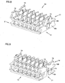
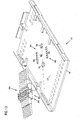
- FIGS. 1 and 2 illustrate an embodiment of a splice tray arrangement 10 having features that are examples of how inventive aspects in accordance with the principles of the present disclosure may be practiced.
- One of the preferred features relates to increasing the splice element density of the splice tray arrangement without reducing storage capacity.
- the splice tray arrangement 10 is used to house spliced fiber optic cables 12.
- spliced fiber optic cables two fiber optic cables are joined or spliced together by a splice element 14.
- the illustrated splice element 14 is a cylindrical, mass fusion splice element used to join multiple optic fibers of a ribbon cable.
- the splice tray arrangement can be constructed and sized for use with other types of splice elements, such as stranded heat shrink splice elements used to join single-fiber cables, for example.
- the splice tray arrangement 10 of the present disclosure generally includes a base or tray 16 and a splice chip arrangement 18 for holding or retaining the splice elements 14. Often, in use, a generous portion of slack cable is provided to permit maintenance or replacement of the splice elements 14 without requiring complete cable replacement.
- the slack cable is stored within an interior storage region 20 of the tray 16. Cable management components 22, such as tabs, are located within the storage region 20 for retaining and managing the slack cable.
- the tray 16 of the splice tray arrangement 10 includes a generally planar bottom surface 24. Tray sides extend upward from or perpendicular to the bottom surface 24. In the illustrated embodiment, the tray sides include two opposing tray sides 26 and a tray side 28 transverse to the two opposing tray sides 26. The transverse tray side 28 is centrally located at a first end 30 of the tray 16. First and second cable access openings 32, 34 are located at opposite corners of the first end 30 of the tray 16 adjacent to the transverse tray side 28. The first and second cable access openings 32, 34 each function as a cable entry and/or a cable exit. A second end 36 of the tray 16 is an open end. The second open end 36 also functions as a cable entry and/or a cable exit of the splice tray arrangement 10.
- the fiber optic cables 12 can enter and exit through any of the first open end 36, the first cable access opening 32, and the second cable access opening 34 of the tray 16.
- the cables can be fixed at a particular entering and exiting location on the tray 16.
- apertures 48 are provided adjacent to the first open end 36 and the first and second cable access openings 32, 34 of the tray 16.
- a tie or other securing device (not shown) placed through the aperture(s) 48 can be used to tie or secure the cable 12 at the particular entering and exiting location.
- the cable management components 22 e.g. tabs of the splice tray arrangement 10 are formed along each of the sides 26, 28 of the tray 16.
- the tabs 22 retain cables within the interior storage region 20 of the tray 16.
- slots 43 are formed in the bottom surface 24 of the tray 16 opposite each of the tabs 22 for manufacturing purposes.
- the splice tray arrangement 10 can further include a cover (not shown).
- the tray 16 includes cover attachment structure 3 8 constructed to receive mating structure of the cover for securing the.cover to the tray.
- the cover attachment structure 38 includes openings 40 formed in at least one of the opposing sides 26 of the tray 16. In an alternative embodiment, the cover attachment structure 38 can be formed in the transverse side 28 of the splice tray 16.
- the tray 16 of the splice tray arrangement 10 is preferably a molded construction.
- the tray 16 can be molded from common engineering materials including common engineering polymers such as polybutylene terephthalate (PBT), polycarbonate (PC), polyethylene ether (PPE), and polystyrene (PS), for example.
- common engineering polymers such as polybutylene terephthalate (PBT), polycarbonate (PC), polyethylene ether (PPE), and polystyrene (PS), for example.
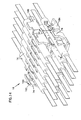
- the splice chip arrangement 18 of the present disclosure preferably includes at least a first splice chip 18A having a stackable configuration.
- the stackable configuration permits multiple splice chips (e.g., 18A and 18B shown in FIG. 2 ) to be stacked upon one another to increase splice element density of the splice tray arrangement 10, without reducing storage capacity.
- FIGS. 3-5 illustrate one of the splice chips (e.g., 18A) of the splice tray arrangement 10.
- the splice chips 18A, 18B shown in FIG. 2 are identical in construction; accordingly, the principles and constructions described with respect to the first splice chip 18A shown in FIGS. 3-5 also apply to the second splice chip 18B.
- the splice chip 18A generally includes a base 44 and a plurality of arms 46.
- the base 44 has a top side 61 ( FIG. 4 ) and a bottom side 63 ( FIG. 5 ).
- the plurality of arms 46 extends or projects upward from the top side 61 of the base 44.
- Each of the arms 46 has a free end 92 ( FIG. 4 ) and an opposite end 94 formed integral with the base 44.
- the arms 46 define slots or channels 52 ( FIG. 5 ) within which the splice elements 14 are placed and held. As shown in FIG. 5 , each of the channels 52 runs parallel to one another.
- the splice chip 18A includes six parallel channels 52.
- the arms 46 of the splice chip 18A are arranged in first and second rows of arms 62, 64.
- a row 54 of dividers 56 is located between the first and second rows of arms 62, 64.
- the channels 52 of the splice chip 18A are each partially defined by at least one arm 46 and one divider 54. As shown in FIG. 5 , the channels 52 have a height H defined by the arms 46. In the illustrated embodiment, the height H is at least about 160 inches to accommodate receipt of a splice element 14 having a diameter of similar dimension.
- the splice chip 18A preferably includes retaining structure 50 for retaining the splice elements 14 within the channels 52.
- the retaining structure 50 includes tabs or heads 80 located at the free ends 92 of the arms 46.
- the heads 80 are constructed and arranged to snap-fit the splice elements 14 securely within the channels 52.
- the splice element 14 rests upon first and second side edges 96, 98 ( FIGS. 3 and 4 ) of the base 44.
- the side edges 96, 98 include detents or cut-outs 99 that cradle the splice elements 14.
- the arms 46 of the splice chip 18A are flexible to provide the snap-fit retaining feature previously described.
- the flexible construction of the arms 46 can be provided by either or both of the choice of manufacturing material, or the dimensional construction of the arms.
- Materials that can be used to manufacture at least the arms 46 of the splice chip 18A include common engineering polymers such as polybutylene terephthalate (PBT), polycarbonate (PC), polyethylene ether (PPE), and polystyrene (PS), for example.
- a splice element 14 is inserted into one of the channels 52 by pressing the splice element 14 downward upon top ramped surfaces 39 ( FIG. 5 ) of the heads 80 of the associated arms 46.
- the downward force flexes the arms 46 outward to accept the splice element 14.
- the splice element 14 is retained within the channel 52 by the heads 80 of the arms 46.
- the dividers 56 of the splice chip 18A can be made of a more rigid construction.
- the dividers 56 for example, do not include retaining structure (e.g. 50) and therefore are not required to flex or function as a snap-fit retainer.
- the splice tray arrangement 10 typically mounts to the bottom surface 24 of the tray 16.
- the splice tray arrangement 10 includes a mounting arrangement 84 that detachably secures the splice chip 18A to the tray 16 without the use of adhesive or additional fasteners.
- the mounting arrangement 84 includes interlocking, longitudinal guides 86 ( FIG. 5 ), 88 ( FIG. 1 ) disposed on each of the splice chip 18A and the tray 16.
- the longitudinal guides 86 of the splice chip 18A includes an integrally formed lip or ledge 90 located at first and second opposite ends 19, 21 of the splice chip 18A.
- the ledges 90 extend laterally outward beyond ends 66, 68 of the base 44, and are offset or spaced a distance from the bottom side 63 of the base 44.
- the base 44 includes an angled portion 45 ( FIG. 5 ) at each of the ends 66, 68 adjacent to the guides 86.
- An interlocking space 47 is provided between each of the guides 86 and the angled portions 45 of the base 44 at the ends 19, 21 of the splice chip 18A.
- the longitudinal guides 88 of the tray 16 includes ribs or tracks 89 that project outward from the bottom surface 24 of the tray.
- the tracks 89 are integrally formed in the bottom surface 24 of the tray 16.
- the tracks 89 have a cross-sectional configuration corresponding to the interlocking space 47 provided by the splice chip 18A.
- the inverse, cross-sectional configuration of the tracks 89 slide within the interlocking spaces 47 of the splice chip 18A to secure the splice chip 18A to the bottom surface 24 of the tray 16.
- the splice chip 18A slides in a lateral direction A, as shown in FIG. 1 , such that the interlocking guides 86, 88 of the mounting arrangement 84 engage one another.
- the splice chip 18A can be secured to the tray 16 by sliding the splice chip 18A in an opposite lateral direction B.
- the interlocking guides 86, 88 of the mounting arrangement 84 are engaged, the splice chip 18A is prevented from movement in a direction transverse to the bottom surface 24 of the tray.
- the splice chip arrangement 18 is preferably constructed to accommodate an increased density of splice elements 14 ( FIG. 2 ) without reducing storage capacity within the splice tray arrangement 10.
- the splice chips 18A, 18B are thereby stackable. That is, the splice chips 18A, 18B are constructed to stack on top of one another at a particular splice chip mounting location 42 ( FIG. 13 ) of the tray 16. As shown in FIG. 13 , the splice chip mounting location 42 is generally defined between the tracks 89 of the mounting arrangement 84.
- each of the splice chips 18A, 18B includes a snap-fit stacking arrangement 60 that detachably secures the splice chips in relation to one another.
- the splice chips 18A, 18B are stacked on top of one another. While referred to as being stacked on top of one another, it will be appreciated that the splice chips 18A, 18B need not be limited to a vertically stacked arrangement. Rather, the phrase "stacked on top of one another" is used for explanatory purposes of the illustrated embodiment.
- the splice chips may be stacked in a front-to-back arrangement depending upon the orientation of the tray, for example.
- the stacking arrangement 60 of the splice chips 18A, 18B is configured to function interchangeably with the mounting arrangement 84 of the splice tray arrangement 10. That is, the stacking arrangement 60 includes the interlocking guides 86 of the mounting arrangement 84 so that both the stacking arrangement 60 and the mounting arrangement 84 function to mount the splice chip to another splice chip, and to mount the splice chip to the tray 16.
- the splice chips 18A, 18B are interchangeable and need not be dedicated as only a stackable chip or tray-mounted chip.
- the stacking arrangement 60 of each of the splice chips 18A, 18B further includes first and second latch members 70, 72 located at the first end 19 of the splice chip 18A, 18B, and a third latch member 74 located at the second opposite end 21 of the splice chip.
- the latch members 70, 72, 74 of each of the splice chips are configured to engage or latch into the interlocking spaces 47 of another splice chip.
- first, second, and third slots 71, 73, 75 are formed in the ends 66, 68 of the base 44 for purposes of manufacturing.
- the slots 71, 73, 75 defined segments of interlocking spaces 47 that correspond to the arrangement of latch members 70, 72, 74.
- the stacked splice chips 18A, 18B are accordingly stacked in an alternating manner to accommodate the arrangement of slots and latch members. That is, opposite ends (e.g., 19 and 21) of the first and second splice chips 18A, 18B are constructed to interlock with one another.
- the ends 66, 68 of the base 44 can be manufactured without slots, thereby permitting same ends (e.g. 19 and 19) of the first and second splice chips to interlock.
- the first and second latch members 70, 72 at the first end 19 of the bottom splice chip 18A are positioned within the interlocking spaces 47 ( FIGS. 10 and 12 ) provided at the second end 21 of the top splice chip 18B.
- the top splice chip 18B is then pivoted such that the third latch member 74 at the second end 21 of the bottom splice chip 18A snap fits into the interlocking space 47 ( FIG. 11 ) provided at the first end 19 of the top splice chip 18B.
- the third latch member 74 of the bottom splice chip 18A can initially be engaged within the interlocking space provided on the top splice chip 18B, and then the first and second latch members snap fit into the associate interlocking spaces 47 at the other end of the top splice chip 18B.
- At least one of the third latch member 74, and the first and second latch members 70, 72 of the stacking arrangement 60 is flexible to provide the snap-fit retaining feature described.
- the flexible construction of the latch member(s) can be provided by either or both of the choice of manufacturing material and the dimensional construction of the latch member(s).
- the bottom side 63 of the base 44 includes at least a first recess 82.
- the recess 82 is sized to receive a guide 58 ( FIG. 3 ) disposed on top of one of the dividers 56 of the splice chip 18A, 18B.
- two guides 58 ( FIG. 3 ) and recesses 82 are provided on the splice chips 18A, 18B.
- the guides 58 and recesses 82 are arranged to assist in properly locating or aligning the top splice chip 18B in relation to the bottom splice chip 18A.
- the guides 58 and recesses 82 further assist in preventing lateral movement of the top splice chip 18B relative to the bottom splice chip 18A when secured in the stacked relationship.
- the first splice chip 18A is attached to the bottom surface 24 of the tray 16.
- the first splice chip 18A slides in the lateral direction A ( FIG. 1 ) so that the interlocking guides 86, 88 of the splice chip 18A and tray 16 engage.
- Flexible securing tabs 76, 78 are provided to prevent the splice chip 18A from inadvertent lateral movement beyond the chip mounting location 42.
- splice elements 14 can then be placed into the channels 52 of the splice chip.
- the second splice chip 18B can be stacked upon the first splice chip 18A.
- the second splice chip 18B is attached to the first splice chip 18A in the manner previously described. Additional splice elements 14 can then be placed and secured within the channels 52 of the second splice chip 18B.
- the splice elements 14 can be placed within the channels 52 of the splice chips 18A, 18B prior to securing the chips to either the tray 16 or one another. As shown in FIG. 14 , a total of twelve splice elements 14 can be held by the illustrated splice chip arrangement 18.
- each of the splice chips 18A, 18B includes a release tab 100 for detaching the top splice chip (e.g., 18B) from the stack of splice chips.
- the release tab 100 is located adjacent to a top edge 102 of the third latch member 74.
- the top splice chip 18B can then be removed from the stack by pivoting the splice chip 18B upward and disengaging the splice chip from the first and second latch members 70, 72 of the bottom splice chip 18A.
- the bottom splice chip 18A can be removed from the tray 16, by pressing one of the flexible securing tabs 76, 78 flush with the bottom surface 24 of the tray 16, and laterally sliding the chip 18A such that the interlocking guides 86, 88 of the splice chip and tray disengage.
- the overall arrangement and construction of the disclosed splice tray arrangement 10 enhances cable management by providing a splice chip arrangement that is easy to use and increases splice element density.
Landscapes
- Physics & Mathematics (AREA)
- General Physics & Mathematics (AREA)
- Optics & Photonics (AREA)
- Engineering & Computer Science (AREA)
- Plasma & Fusion (AREA)
- Light Guides In General And Applications Therefor (AREA)
- Stackable Containers (AREA)
- Packages (AREA)
Claims (17)
- Spleiß-Chip-Anordnung (18), die an einem Spleißträger (16) angebracht ist, wobei die Spleiß-Chip-Anordnung umfasst:a) einen ersten Spleiß-Chip (18A) und einen zweiten Spleiß-Chip (18B), die in einem gestapelten Verhältnis aneinander befestigt sind, wobei der erste bzw. der zweite Spleiß-Chip umfasst:i) eine Basis (44) mit einem ersten Ende (66) und einem zweiten, entgegen gesetzten Ende (68);ii) mehrere Kanäle (52), die dazu bemessen sind, Spleißelemente (14) aufzunehmen;iii) ein Einklinkteil (70, 72, 74), das sich am ersten bzw. zweiten Ende des Spleiß-Chips befindet; undiv) eine Leiste (90), die sich von einer Oberfläche der Basis am ersten bzw. zweiten Ende des Spleiß-Chips erstreckt;v) wobei ein Formschlussraum zwischen der Leiste (90) bzw. einem angewinkelten Abschnitt (45) der Basis gebildet ist, der sich unter der Leiste befindet;b) wobei die Einklinkteile und die Formschlussräume (47) so zusammenwirken, dass das erste Ende des ersten Spleiß-Chips sich verschwenkend mit dem zweien Ende des zweiten Spleiß-Chips verbindet, und wobei das zweite Ende des ersten Spleiß-Chips am ersten Ende des zweiten Spleiß-Chips einschnappt;c) wobei der erste und/oder zweite Spleiß-Chip ein Freisetzungselement (100) umfasst, um den ersten und den zweiten Spleiß-Chip voneinander zu lösen.
- Spleiß-Chip-Anordnung nach Anspruch 1, wobei das Freisetzungselement eine Freisetzungslasche (100) ist.
- Spleiß-Chip-Anordnung nach Anspruch 1, wobei die Einklinkteile und die Formschlussräume des ersten und zweiten Spleiß-Chips dazu ausgelegt sind, die Spleiß-Chips in Bezug aufeinander lösbar zu befestigen, und zwar so, dass jeder Spleiß-Chip selektiv entweder in einer oberen Position in Bezug auf den anderen Spleiß-Chip oder einer unteren Position in Bezug auf den anderen Spleiß-Chip positionierbar ist.
- Spleiß-Chip-Anordnung nach Anspruch 3, wobei der Formschlussraum des ersten und zweiten Spleiß-Chips darüber hinaus dazu ausgelegt ist, die Spleiß-Chip-Anordnung selektiv an einem Träger (16) anzubringen.
- Spleiß-Chip-Anordnung nach Anspruch 1, darüber hinaus eine Ausnehmung (82), die in einer Bodenfläche der Basis des ersten oder zweiten Spleiß-Chips ausgebildet ist, und eine Führungsstruktur (58) umfassend, die sich angrenzend an die Kanäle des anderen Spleiß-Chips der ersten und zweiten Spleiß-Chips befindet, wobei die Ausnehmung des einen Spleiß-Chips dazu ausgelegt ist, die Führungsstruktur des anderen Spleiß-Chips aufzunehmen, um eine seitliche Bewegung der Spleiß-Chips in Bezug aufeinander zu verhindern.
- Spleiß-Chip-Anordnung nach Anspruch 1, darüber hinaus eine Ausnehmung (82), die in einer Bodenfläche der Basis des ersten oder zweiten Spleiß-Chips ausgebildet ist, und eine Ausrichtungsführung (58) umfassend, die sich angrenzend an die Kanäle des anderen Spleiß-Chips der ersten und zweiten Spleiß-Chips befindet, wobei die Ausnehmung des einen Spleiß-Chips dazu ausgelegt ist, die Ausrichtungsführung des anderen Spleiß-Chips aufzunehmen, um die Spleiß-Chips in Bezug aufeinander auszurichten.
- Spleißträgeranordnung (10), Folgendes umfassend:a) einen Träger (16) mit einer Spleiß-Chip-Anbringungsstelle; undb) eine Spleiß-Chip-Anordnung (18) nach Anspruch 1 oder 2, wobeider erste Spleiß-Chip an der Anbringungsstelle positioniert ist, wobei der erste Spleiß-Chip eine Vielzahl von Spleiß-Haltestrukturen umfasst, wobei der erste Spleiß-Chip eine Anbringungsstruktur umfasst, die so ausgelegt ist, dass der erste Spleiß-Chip an der Anbringungsstelle seitlich in Position gleitet; und
der zweite Spleiß-Chip am ersten Spleiß-Chip an der Anbringungsstelle angeordnet ist, wobei der zweite Spleiß-Chip eine Vielzahl von Spleißhaltestrukturen umfasst. - Spleißträgeranordnung nach Anspruch 7, wobei der erste und zweite Spleiß-Chip jeweils Formschlussführungen (70, 72, 74, 90) zum Anbringen am Träger oder am anderen Spleiß-Chip der ersten und zweiten Spleiß-Chips umfassen.
- Spleißträgeranordnung nach Anspruch 7, wobei der eine erste oder zweite Spleiß-Chip eine Ausnehmung (82) umfasst, die in einer Bodenfläche der Basis ausgebildet ist, und wobei der andere erste oder zweite Spleiß-Chip eine Ausrichtungsführung (58) umfasst, wobei die Ausnehmung und die Ausrichtungsführung dazu eingerichtet sind, die Spleiß-Chips in Bezug aufeinander auszurichten.
- Spleißträgeranordnung nach Anspruch 7, wobei der eine erste oder zweite Spleiß-Chip ein Einklinkteil (70, 72, 74) und der andere erste oder zweite Spleiß-Chip einen Formschlussraum (47) umfasst, der zwischen einer Basis (44) und einer über die Basis nach außen vorstehenden Leiste (90) ausgebildet ist, wobei das Einklinkteil des einen Spleiß-Chips mit dem Formschlussraum des anderen Spleiß-Chips in Eingriff ist.
- Spleißträgeranordnung nach Anspruch 10, wobei das Einklinkteil des einen Spleiß-Chips in den Formschlussraum des anderen Spleiß-Chips einschnappt.
- Spleißträgeranordnung nach Anspruch 7, wobei der erste und zweite Spleiß-Chip zusammen eine Schnappbefestigung eingehen.
- Verfahren zum Zusammenbauen einer Spleißträgeranordnung (10) nach Anspruch 1, wobei das Verfahren die folgenden Schritte umfasst:a) Befestigen eines ersten Spleiß-Chips (18A) an einer Anbringungsstelle an einem Träger (16), indem der erste Spleiß-Chip in einer seitlichen Richtung entlang einer Anbringungsfläche des Trägers verschoben wird; undb) Befestigen eines zweiten Spleiß-Chips (18B) an der Anbringungsstelle am ersten Spleiß-Chip, wobei das Befestigen umfasst, den ersten und zweiten Spleiß-Chip in Eingriff zu bringen und den zweiten Spleiß-Chip in Bezug auf den ersten Spleiß-Chip zu verschwenken, um eine Schnappverbindung zu bewirken.
- Verfahren nach Anspruch 13, darüber hinaus ein Positionieren einer Anzahl von Spleißelementen in sowohl dem ersten als auch zweiten Spleiß-Chip umfassend.
- Verfahren nach Anspruch 13, wobei der Schritt des Befestigens des zweiten Spleiß-Chips an der Anbringungsstelle am ersten Spleiß-Chip bewerkstelligt wird, ohne den Stauraum im Träger zu verkleinern.
- Verfahren nach Anspruch 13, wobei der erste Spleiß-Chip und der Träger jeweils darauf vorgesehene formschlüssige Längsführungen (86, 88) haben, und das Verschieben so erfolgt, dass die formschlüssigen Längsführungen des ersten Spleiß-Chips in die formschlüssigen Längsführungen des Trägers eingreifen.
- Verfahren nach Anspruch 13 oder 16, wobei das in Eingriff bringen darin besteht, Einklinkteile (70, 72) an einem ersten Ende (19) des ersten Spleiß-Chips in den an einem zweiten Ende (21) des zweiten Spleiß-Chips vorgesehenen Formschlussräumen (47) zu positionieren, und das Verschwenken darin besteht, den zweiten Spleiß-Chip so zu verschwenken, dass ein Einklinkteil (74) an einem zweiten Ende (21) des ersten Spleiß-Chips in dem an einem ersten Ende (19) des zweiten Spleiß-Chips vorgesehenen Formschlussraum (47) einschnappt.
Applications Claiming Priority (2)
| Application Number | Priority Date | Filing Date | Title |
|---|---|---|---|
| US11/212,470 US7310471B2 (en) | 2005-08-25 | 2005-08-25 | Stackable splice chip device |
| PCT/US2006/032859 WO2007024912A1 (en) | 2005-08-25 | 2006-08-22 | Stackable splice chip device |
Publications (2)
| Publication Number | Publication Date |
|---|---|
| EP1929348A1 EP1929348A1 (de) | 2008-06-11 |
| EP1929348B1 true EP1929348B1 (de) | 2011-10-12 |
Family
ID=37433729
Family Applications (1)
| Application Number | Title | Priority Date | Filing Date |
|---|---|---|---|
| EP06802138A Not-in-force EP1929348B1 (de) | 2005-08-25 | 2006-08-22 | Stapelbare spleiss-chip-einrichtung |
Country Status (10)
| Country | Link |
|---|---|
| US (3) | US7310471B2 (de) |
| EP (1) | EP1929348B1 (de) |
| JP (1) | JP2009506362A (de) |
| KR (1) | KR20080039489A (de) |
| CN (1) | CN101243347B (de) |
| AT (1) | ATE528677T1 (de) |
| AU (1) | AU2006283165B2 (de) |
| BR (1) | BRPI0615366A2 (de) |
| ES (1) | ES2370263T3 (de) |
| WO (1) | WO2007024912A1 (de) |
Cited By (1)
| Publication number | Priority date | Publication date | Assignee | Title |
|---|---|---|---|---|
| IT202000007045A1 (it) | 2020-04-02 | 2021-10-02 | Prysmian Spa | Vassoio per giunzioni di fibra ottica |
Families Citing this family (112)
| Publication number | Priority date | Publication date | Assignee | Title |
|---|---|---|---|---|
| US7310471B2 (en) * | 2005-08-25 | 2007-12-18 | Adc Telecommunications, Inc. | Stackable splice chip device |
| US7272291B2 (en) * | 2005-08-25 | 2007-09-18 | Adc Telecommunications, Inc. | Splice chip device |
| DE102007009223B4 (de) * | 2007-02-26 | 2011-03-17 | Adc Gmbh | Zugentlastung für Kabel |
| US7822310B2 (en) | 2007-02-28 | 2010-10-26 | Corning Cable Systems Llc | Fiber optic splice trays |
| US8798427B2 (en) | 2007-09-05 | 2014-08-05 | Corning Cable Systems Llc | Fiber optic terminal assembly |
| WO2009048795A1 (en) * | 2007-10-09 | 2009-04-16 | 3M Innovative Properties Company | Splice holder with ejector |
| DE202008002812U1 (de) * | 2008-02-28 | 2008-04-24 | CCS Technology, Inc., Wilmington | Haltevorrichtung für Spleißschutzeinrichtungen mit in den Spleißschutzeinrichtungen aufgenommenen Spleißen von Lichtwellenleitern |
| US7889961B2 (en) | 2008-03-27 | 2011-02-15 | Corning Cable Systems Llc | Compact, high-density adapter module, housing assembly and frame assembly for optical fiber telecommunications |
| WO2009131770A2 (en) * | 2008-04-21 | 2009-10-29 | Afl Telecommunications Llc | Fiber optic splice tray |
| WO2009131895A2 (en) * | 2008-04-21 | 2009-10-29 | Adc Telecommunications, Inc. | Fiber optic splice tray |
| US8135257B2 (en) * | 2008-08-29 | 2012-03-13 | Corning Cable Systems Llc | Structures for managing and mounting cable assemblies |
| US8290333B2 (en) | 2008-08-29 | 2012-10-16 | Corning Cable Systems Llc | Fiber optic cable assemblies with furcation bodies having features for manufacturing and methods of making the same |
| US8452148B2 (en) | 2008-08-29 | 2013-05-28 | Corning Cable Systems Llc | Independently translatable modules and fiber optic equipment trays in fiber optic equipment |
| US8301004B2 (en) * | 2008-08-29 | 2012-10-30 | Corning Cable Systems Llc | Fiber optic cable assemblies employing a furcation body having anti-rotation feature |
| US11294136B2 (en) | 2008-08-29 | 2022-04-05 | Corning Optical Communications LLC | High density and bandwidth fiber optic apparatuses and related equipment and methods |
| US8086084B2 (en) * | 2008-09-09 | 2011-12-27 | Adc Telecommunications, Inc. | Fiber optic splice tray |
| WO2010040256A1 (en) | 2008-10-09 | 2010-04-15 | Corning Cable Systems Llc | Fiber optic terminal having adapter panel supporting both input and output fibers from an optical splitter |
| US8879882B2 (en) | 2008-10-27 | 2014-11-04 | Corning Cable Systems Llc | Variably configurable and modular local convergence point |
| US8165442B2 (en) * | 2008-11-06 | 2012-04-24 | Ofs Fitel, Llc | System for securing fiber optic devices in management trays |
| WO2010083369A1 (en) * | 2009-01-15 | 2010-07-22 | Adc Telecommunications, Inc. | Fiber optic module, chassis and adapter |
| EP2221932B1 (de) | 2009-02-24 | 2011-11-16 | CCS Technology Inc. | Haltevorrichtung für ein Kabel oder eine Anordnung zur Verwendung mit einem Kabel |
| EP2237091A1 (de) | 2009-03-31 | 2010-10-06 | Corning Cable Systems LLC | Lösbar montierbares LWL-Leitungsendgerät |
| US8699838B2 (en) | 2009-05-14 | 2014-04-15 | Ccs Technology, Inc. | Fiber optic furcation module |
| US9075216B2 (en) | 2009-05-21 | 2015-07-07 | Corning Cable Systems Llc | Fiber optic housings configured to accommodate fiber optic modules/cassettes and fiber optic panels, and related components and methods |
| US8280216B2 (en) | 2009-05-21 | 2012-10-02 | Corning Cable Systems Llc | Fiber optic equipment supporting moveable fiber optic equipment tray(s) and module(s), and related equipment and methods |
| US7945136B2 (en) * | 2009-06-19 | 2011-05-17 | Corning Cable Systems Llc | Mounting of fiber optic cable assemblies within fiber optic shelf assemblies |
| EP2443497B1 (de) | 2009-06-19 | 2020-03-04 | Corning Cable Systems LLC | Glasfaservorrichtungen mit hoher dichte |
| US8712206B2 (en) | 2009-06-19 | 2014-04-29 | Corning Cable Systems Llc | High-density fiber optic modules and module housings and related equipment |
| CN102804014A (zh) | 2009-06-19 | 2012-11-28 | 康宁电缆系统有限责任公司 | 高光纤电缆封装密度装置 |
| US8467651B2 (en) | 2009-09-30 | 2013-06-18 | Ccs Technology Inc. | Fiber optic terminals configured to dispose a fiber optic connection panel(s) within an optical fiber perimeter and related methods |
| US8625950B2 (en) | 2009-12-18 | 2014-01-07 | Corning Cable Systems Llc | Rotary locking apparatus for fiber optic equipment trays and related methods |
| EP2354824A1 (de) * | 2010-01-29 | 2011-08-10 | CCS Technology Inc. | Hybridstecker |
| US8593828B2 (en) | 2010-02-04 | 2013-11-26 | Corning Cable Systems Llc | Communications equipment housings, assemblies, and related alignment features and methods |
| WO2011112764A1 (en) | 2010-03-10 | 2011-09-15 | Corning Cable Systems Llc | Fiber optic pigtail assembly allowing single and mass splicing |
| US9547144B2 (en) | 2010-03-16 | 2017-01-17 | Corning Optical Communications LLC | Fiber optic distribution network for multiple dwelling units |
| US8913866B2 (en) | 2010-03-26 | 2014-12-16 | Corning Cable Systems Llc | Movable adapter panel |
| US8792767B2 (en) | 2010-04-16 | 2014-07-29 | Ccs Technology, Inc. | Distribution device |
| AU2011265751B2 (en) | 2010-04-16 | 2015-09-10 | Corning Optical Communications LLC | Sealing and strain relief device for data cables |
| EP2381284B1 (de) | 2010-04-23 | 2014-12-31 | CCS Technology Inc. | Glasfaserverteilungsvorrichtung für Unterboden |
| US9519118B2 (en) | 2010-04-30 | 2016-12-13 | Corning Optical Communications LLC | Removable fiber management sections for fiber optic housings, and related components and methods |
| US8385711B2 (en) | 2010-04-30 | 2013-02-26 | Corning Cable Systems Llc | Multi-configurable splice holder |
| US8660397B2 (en) | 2010-04-30 | 2014-02-25 | Corning Cable Systems Llc | Multi-layer module |
| US9632270B2 (en) | 2010-04-30 | 2017-04-25 | Corning Optical Communications LLC | Fiber optic housings configured for tool-less assembly, and related components and methods |
| US8705926B2 (en) | 2010-04-30 | 2014-04-22 | Corning Optical Communications LLC | Fiber optic housings having a removable top, and related components and methods |
| US9075217B2 (en) | 2010-04-30 | 2015-07-07 | Corning Cable Systems Llc | Apparatuses and related components and methods for expanding capacity of fiber optic housings |
| US8879881B2 (en) | 2010-04-30 | 2014-11-04 | Corning Cable Systems Llc | Rotatable routing guide and assembly |
| US9720195B2 (en) | 2010-04-30 | 2017-08-01 | Corning Optical Communications LLC | Apparatuses and related components and methods for attachment and release of fiber optic housings to and from an equipment rack |
| US8254742B2 (en) * | 2010-05-11 | 2012-08-28 | Commscope, Inc. Of North Carolina | Splice holder |
| US8718436B2 (en) | 2010-08-30 | 2014-05-06 | Corning Cable Systems Llc | Methods, apparatuses for providing secure fiber optic connections |
| AU2015224528B2 (en) * | 2010-10-19 | 2017-09-14 | Corning Cable Systems Llc | Local convergence point for multiple dwelling unit fiber optic distribution network |
| US9720197B2 (en) | 2010-10-19 | 2017-08-01 | Corning Optical Communications LLC | Transition box for multiple dwelling unit fiber optic distribution network |
| US9279951B2 (en) | 2010-10-27 | 2016-03-08 | Corning Cable Systems Llc | Fiber optic module for limited space applications having a partially sealed module sub-assembly |
| US8662760B2 (en) | 2010-10-29 | 2014-03-04 | Corning Cable Systems Llc | Fiber optic connector employing optical fiber guide member |
| US9116324B2 (en) | 2010-10-29 | 2015-08-25 | Corning Cable Systems Llc | Stacked fiber optic modules and fiber optic equipment configured to support stacked fiber optic modules |
| WO2012074982A1 (en) | 2010-11-30 | 2012-06-07 | Corning Cable Systems Llc | Fiber device holder and strain relief device |
| WO2012106510A2 (en) | 2011-02-02 | 2012-08-09 | Corning Cable Systems Llc | Dense fiber optic connector assemblies and related connectors and cables suitable for establishing optical connections for optical backplanes in equipment racks |
| US9052468B2 (en) * | 2011-03-04 | 2015-06-09 | Corning Cable Systems Llc | Fiber optic adapter mount |
| US9182563B2 (en) | 2011-03-31 | 2015-11-10 | Adc Telecommunications, Inc. | Adapter plate for fiber optic module |
| US9008485B2 (en) | 2011-05-09 | 2015-04-14 | Corning Cable Systems Llc | Attachment mechanisms employed to attach a rear housing section to a fiber optic housing, and related assemblies and methods |
| US8792753B2 (en) * | 2011-06-30 | 2014-07-29 | General Electric Company | Method and system for a fiber optic sensor |
| US8989547B2 (en) | 2011-06-30 | 2015-03-24 | Corning Cable Systems Llc | Fiber optic equipment assemblies employing non-U-width-sized housings and related methods |
| US9110266B2 (en) | 2011-07-29 | 2015-08-18 | Corning Cable Systems Llc | Fiber optic cables seal and/or strain relief members, and related assemblies and methods |
| JP5325967B2 (ja) * | 2011-11-28 | 2013-10-23 | 株式会社フジクラ | 光ファイバ接続用ユニット |
| CN103765266A (zh) | 2011-08-09 | 2014-04-30 | 株式会社藤仓 | 机械接头单元、机械接头用连接工具以及光纤连接施工方法 |
| US8953924B2 (en) | 2011-09-02 | 2015-02-10 | Corning Cable Systems Llc | Removable strain relief brackets for securing fiber optic cables and/or optical fibers to fiber optic equipment, and related assemblies and methods |
| US9417401B2 (en) | 2011-09-06 | 2016-08-16 | Commscope Technologies Llc | Adapter for fiber optic module |
| WO2013056018A2 (en) * | 2011-10-14 | 2013-04-18 | Heyco, Inc. | Cable holder |
| US9207422B2 (en) * | 2011-10-26 | 2015-12-08 | All Systems Broadband, Inc. | Holders for optical fiber splice sleeves and passive optical components |
| US8559784B2 (en) * | 2011-10-26 | 2013-10-15 | All Systems Broadband, Inc. | Modular assembly for supporting fiber optic splices |
| US9038832B2 (en) | 2011-11-30 | 2015-05-26 | Corning Cable Systems Llc | Adapter panel support assembly |
| US9219546B2 (en) | 2011-12-12 | 2015-12-22 | Corning Optical Communications LLC | Extremely high frequency (EHF) distributed antenna systems, and related components and methods |
| US8842962B2 (en) | 2012-01-27 | 2014-09-23 | Corning Cable Systems Llc | Fiber optic cable strain relief device and method |
| US10110307B2 (en) | 2012-03-02 | 2018-10-23 | Corning Optical Communications LLC | Optical network units (ONUs) for high bandwidth connectivity, and related components and methods |
| AU2013266230B2 (en) | 2012-05-25 | 2017-02-16 | Commscope Technologies Llc | Splice chips for optical fiber splice cassettes |
| US9004778B2 (en) | 2012-06-29 | 2015-04-14 | Corning Cable Systems Llc | Indexable optical fiber connectors and optical fiber connector arrays |
| US9250409B2 (en) | 2012-07-02 | 2016-02-02 | Corning Cable Systems Llc | Fiber-optic-module trays and drawers for fiber-optic equipment |
| US9049500B2 (en) | 2012-08-31 | 2015-06-02 | Corning Cable Systems Llc | Fiber optic terminals, systems, and methods for network service management |
| US9042702B2 (en) | 2012-09-18 | 2015-05-26 | Corning Cable Systems Llc | Platforms and systems for fiber optic cable attachment |
| US8909019B2 (en) | 2012-10-11 | 2014-12-09 | Ccs Technology, Inc. | System comprising a plurality of distribution devices and distribution device |
| ES2606755T3 (es) | 2012-10-26 | 2017-03-27 | Ccs Technology, Inc. | Dispositivo de alivio de tensión para cables y dispositivo de distribución de fibras ópticas |
| ES2551077T3 (es) | 2012-10-26 | 2015-11-16 | Ccs Technology, Inc. | Unidad de gestión de fibra óptica y dispositivo de distribución de fibra óptica |
| WO2014071021A1 (en) * | 2012-10-31 | 2014-05-08 | Adc Telecommunications, Inc. | Anchoring cables to rack with cable clamp arrangements |
| EP2929387B1 (de) * | 2012-12-07 | 2018-10-31 | Corning Optical Communications LLC | Faseroptische module mit spleisshalterung und fasermanagement |
| US8985862B2 (en) | 2013-02-28 | 2015-03-24 | Corning Cable Systems Llc | High-density multi-fiber adapter housings |
| US9606315B2 (en) | 2013-03-15 | 2017-03-28 | All Systems Broadband, Inc. | Optical fiber ribbon storage |
| US9488793B2 (en) | 2013-09-10 | 2016-11-08 | Corning Optical Communications LLC | Combined optical fiber and power cable |
| US10061089B2 (en) * | 2013-09-20 | 2018-08-28 | Adva Optical Networking Se | Fiber optic component holding device for fibers in side-by-side contact |
| EP2960698B1 (de) * | 2014-06-27 | 2017-08-09 | CCS Technology, Inc. | Spleißhalterung für Spleißschutze zum Schutz von Spleißen zwischen optischen Fasern durch Einzelfaserspleißung |
| EP3259630B1 (de) * | 2015-02-17 | 2021-09-15 | Corning Research & Development Corporation | Hochkonfigurierbare faseroptische verbindungsschale |
| USD781788S1 (en) * | 2015-03-31 | 2017-03-21 | Optical Cable Corporation | Splice tray cabinet |
| US10514519B2 (en) * | 2016-01-14 | 2019-12-24 | Ppc Broadband, Inc. | Stackable splitters |
| KR200485520Y1 (ko) * | 2016-02-22 | 2018-01-19 | 주식회사 에이.제이.월드 | 광접속 트레이 및 이를 포함하는 광접속 함체 |
| US10295771B2 (en) | 2016-05-03 | 2019-05-21 | Corning Optical Communications LLC | Telecommunications terminal with removable modules |
| MX387950B (es) * | 2016-10-25 | 2025-03-19 | Commscope Technologies Llc | Sujetador para fibra y metodo de uso |
| EP3698190B1 (de) * | 2017-10-17 | 2024-05-29 | Corning Research & Development Corporation | Spleisskassette für optische fasern |
| CN107976754A (zh) * | 2017-12-14 | 2018-05-01 | 江苏亨通光电股份有限公司 | 一种光纤箱内置理线盒装置 |
| EP3785057B1 (de) * | 2018-04-23 | 2023-09-13 | CommScope Technologies LLC | Mechanische verbindungsschnittstelle für eine optische telekommunikationskomponente |
| US10852498B2 (en) * | 2018-05-24 | 2020-12-01 | Clearfield, Inc. | Optical fiber distribution systems and components |
| EP3803485A1 (de) * | 2018-05-30 | 2021-04-14 | Corning Research & Development Corporation | Modulares glasfaserspleissablagesystem |
| EP3745177A1 (de) * | 2019-05-29 | 2020-12-02 | CommScope Technologies LLC | Adapter für faseroptischen halter, anordnung und verfahren |
| US10845561B1 (en) | 2019-06-28 | 2020-11-24 | Afl Telecommunications Llc | Fiber optic cassettes and splice modules |
| WO2021026879A1 (en) * | 2019-08-15 | 2021-02-18 | Commscope Technologies Llc | Dual-sided splice cassette |
| WO2021195371A1 (en) * | 2020-03-27 | 2021-09-30 | All Systems Broadband, Inc. | Stackable fiber optic splice holder |
| US11686911B2 (en) | 2020-09-17 | 2023-06-27 | Panduit Corp. | Optical distribution and splice frame including enclosures |
| US11971598B2 (en) | 2021-02-18 | 2024-04-30 | Commscope Technologies Llc | Tray arrangements for cassettes |
| US11740421B2 (en) * | 2021-02-18 | 2023-08-29 | Commscope Technologies Llc | Communications panel system |
| US11927808B2 (en) | 2021-04-16 | 2024-03-12 | Commscope Technologies Llc | Holder for an optical component |
| US12105339B2 (en) * | 2021-06-04 | 2024-10-01 | Sumitomo Electric Industries, Ltd. | Wiring module, frame body for wiring module, and forming method for forming wiring module |
| WO2023048730A1 (en) * | 2021-09-27 | 2023-03-30 | All Systems Broadband, Inc. | Stackable fiber optic splice holder with space efficient splice holder retention |
| US12443001B2 (en) * | 2021-11-01 | 2025-10-14 | Preformed Line Products Co. | Extendable splice tray |
| US12259590B2 (en) * | 2021-11-29 | 2025-03-25 | Corning Research & Development Corporation | Fiber-optic apparatus |
| EP4286910A1 (de) * | 2022-06-01 | 2023-12-06 | Corning Research & Development Corporation | Abnehmbarer optischer organisator |
Citations (1)
| Publication number | Priority date | Publication date | Assignee | Title |
|---|---|---|---|---|
| WO2007039585A1 (en) * | 2005-10-05 | 2007-04-12 | Tyco Electronics Raychem Nv | Optical fibre connection devices |
Family Cites Families (56)
| Publication number | Priority date | Publication date | Assignee | Title |
|---|---|---|---|---|
| US4840449A (en) | 1988-01-27 | 1989-06-20 | American Telephone And Telegraph Company, At&T Bell Laboratories | Optical fiber splice organizer |
| GB8805017D0 (en) | 1988-03-02 | 1988-03-30 | British Telecomm | Splice tray |
| US4900123A (en) | 1988-08-29 | 1990-02-13 | Gte Products Corporation | 1550 nm fiber distribution panel |
| GB2237121B (en) | 1989-10-10 | 1993-07-21 | Bowthorpe Hellermann Ltd | Optical fibre splice storage enclosure |
| US5074635A (en) | 1990-05-21 | 1991-12-24 | Minnesota Mining And Manufacturing Company | Splice tray and method |
| US5185845A (en) * | 1990-12-13 | 1993-02-09 | At&T Bell Laboratories | Optical fiber closure having enhanced storage capability |
| US5119459A (en) | 1991-02-15 | 1992-06-02 | Porta Systems Corp. | Optical fiber storage and distribution cabinet |
| US5189725A (en) * | 1992-01-28 | 1993-02-23 | At&T Bell Laboratories | Optical fiber closure |
| US5323480A (en) | 1992-11-25 | 1994-06-21 | Raychem Corporation | Fiber optic splice closure |
| DE4302837A1 (de) | 1993-01-28 | 1994-08-18 | Krone Ag | Gehäuse für passive optische Komponenten |
| US5363467A (en) | 1993-05-28 | 1994-11-08 | Minnesota Mining And Manufacturing Company | Compact fiber optic housing |
| US5548678A (en) | 1993-09-10 | 1996-08-20 | British Telecommunications Public Limited Company | Optical fibre management system |
| US5490229A (en) | 1993-12-08 | 1996-02-06 | At&T Ipm Corp. | Slidably mounted optical fiber distribution tray |
| DE4415218C1 (de) | 1994-04-26 | 1995-10-19 | Krone Ag | Gehäuse für optische Komponenten |
| US5519804A (en) | 1994-06-22 | 1996-05-21 | At&T Corp. | Universal splice tray |
| GB2305739B (en) | 1994-09-28 | 1998-11-04 | Telephone Cables Ltd | Optical fibre splice tray |
| US5450518A (en) | 1994-10-13 | 1995-09-12 | At&T Corp. | Optical fiber cable splice closure |
| US5689605A (en) | 1995-02-09 | 1997-11-18 | Lucent Technologies Inc. | Splice holder assembly for an optical fiber cable splice closure |
| NZ303594A (en) | 1995-03-31 | 1999-01-28 | Minnesota Mining & Mfg | Optical fibre splice tray arrangement |
| US5590234A (en) | 1995-03-31 | 1996-12-31 | Minnesota Mining And Manufacturing Company | Fiber optic splice organizers |
| US5553183A (en) | 1995-04-03 | 1996-09-03 | Antec Corp. | Apparatus for and methods of splitting fiber optic signals |
| FR2734651B1 (fr) | 1995-05-24 | 1997-06-20 | Alcatel Cable Interface | Boitier de raccordement de fibre optique |
| US5577151A (en) | 1995-08-15 | 1996-11-19 | The Whitaker Corporation | Optical fiber splice tray and cover |
| US5835657A (en) | 1995-12-08 | 1998-11-10 | Psi Telecommunications, Inc. | Fiber optic splice tray |
| US5647045A (en) | 1996-02-23 | 1997-07-08 | Leviton Manufacturing Co., Inc. | Multi-media connection housing |
| DE19611770C2 (de) | 1996-03-14 | 1998-04-09 | Krone Ag | Managementfähige Spleißkassette |
| KR100242412B1 (ko) * | 1996-10-25 | 2000-03-02 | 윤종용 | 광섬유 증폭기의 광학소자 고정용 패키징 박스 |
| US5825962A (en) | 1996-12-31 | 1998-10-20 | Siecor Corporation | Optical fiber splice housing |
| US5896486A (en) | 1997-05-01 | 1999-04-20 | Lucent Technologies Inc. | Mass splice tray for optical fibers |
| KR100261762B1 (ko) | 1997-12-02 | 2000-07-15 | 이계철 | 리본형광섬유의 보호지지판 |
| US6009225A (en) | 1998-05-26 | 1999-12-28 | Ray; Craig D. | Fiber optic drop splice closure and related methods |
| US6215938B1 (en) | 1998-09-21 | 2001-04-10 | Adc Telecommunications, Inc. | Fiber optic cabinet and tray |
| US6353697B1 (en) * | 1999-07-30 | 2002-03-05 | Lucent Technologies, Inc. | Modular layered splice holder |
| US6285815B1 (en) | 1999-09-07 | 2001-09-04 | Lucent Technologies Inc. | High density fusion splice holder |
| US6249636B1 (en) | 1999-09-07 | 2001-06-19 | Lucent Technologies, Inc. | High density fusion splice holder |
| US6259851B1 (en) | 1999-09-17 | 2001-07-10 | Lucent Technologies Inc. | High density fiber splice holder |
| US6456772B1 (en) | 1999-09-21 | 2002-09-24 | Avaya Technology Corp. | System for removable attachment of two objects |
| US6226436B1 (en) | 1999-11-18 | 2001-05-01 | Lucent Technologies, Inc. | Fiber optical pedestal |
| US6427045B1 (en) | 2000-03-08 | 2002-07-30 | Marconi Communications, Inc. | Splice tray for use in splicing fiber optic cables and housing therefor |
| US6687450B1 (en) | 2000-05-15 | 2004-02-03 | Tyco Electronics Raychem Nv | Break-out device |
| GB2367379B (en) | 2000-09-27 | 2004-08-25 | Krone Gmbh | Opitcal fibre connection housing |
| GB2367378B (en) | 2000-09-27 | 2004-08-25 | Krone Gmbh | Patch panel |
| US6504989B1 (en) | 2000-10-23 | 2003-01-07 | Onetta, Inc. | Optical equipment and methods for manufacturing optical communications equipment for networks |
| US6845207B2 (en) | 2001-02-12 | 2005-01-18 | Fiber Optic Network Solutions Corp. | Optical fiber enclosure system |
| US20020118944A1 (en) | 2001-02-28 | 2002-08-29 | Corning Cable Systems Llc | Optical fiber storage reel |
| US6512876B2 (en) | 2001-04-25 | 2003-01-28 | Lucent Technologies Inc. | Fiber splice tray |
| US6944387B2 (en) | 2001-04-30 | 2005-09-13 | Telect, Inc. | Fiber optic connector tray system |
| US6580866B2 (en) | 2001-05-16 | 2003-06-17 | Lucent Technologies Inc. | Fiber splice holder with protected slack storage feature |
| US6567601B2 (en) | 2001-06-19 | 2003-05-20 | Lucent Technologies Inc. | Fiber-optic cable routing and management system and components |
| US6744962B2 (en) | 2001-10-25 | 2004-06-01 | Uniseal, Inc. | Fiberoptic splice closure |
| US6701056B2 (en) * | 2002-01-02 | 2004-03-02 | Wavesplitter Technologies, Inc. | Modular, variably configurable retainer assembly for optical components |
| US6798966B2 (en) | 2002-11-01 | 2004-09-28 | Hon Hai Precision Ind. Co., Ltd | Dense wavelength division multiplexer module |
| US6915059B2 (en) | 2003-05-30 | 2005-07-05 | Lucent Technologies Inc. | Stackable optical fiber splice tray and mounting shelves |
| US6801704B1 (en) | 2003-05-30 | 2004-10-05 | Lucent Technologies Inc. | Fiber optics splice holder |
| US7310471B2 (en) * | 2005-08-25 | 2007-12-18 | Adc Telecommunications, Inc. | Stackable splice chip device |
| US7272291B2 (en) * | 2005-08-25 | 2007-09-18 | Adc Telecommunications, Inc. | Splice chip device |
-
2005
- 2005-08-25 US US11/212,470 patent/US7310471B2/en not_active Expired - Fee Related
-
2006
- 2006-08-22 KR KR1020087006058A patent/KR20080039489A/ko not_active Ceased
- 2006-08-22 BR BRPI0615366-6A patent/BRPI0615366A2/pt not_active Application Discontinuation
- 2006-08-22 EP EP06802138A patent/EP1929348B1/de not_active Not-in-force
- 2006-08-22 ES ES06802138T patent/ES2370263T3/es active Active
- 2006-08-22 CN CN2006800296856A patent/CN101243347B/zh not_active Expired - Fee Related
- 2006-08-22 WO PCT/US2006/032859 patent/WO2007024912A1/en not_active Ceased
- 2006-08-22 AU AU2006283165A patent/AU2006283165B2/en not_active Ceased
- 2006-08-22 AT AT06802138T patent/ATE528677T1/de not_active IP Right Cessation
- 2006-08-22 JP JP2008528092A patent/JP2009506362A/ja active Pending
-
2007
- 2007-12-14 US US12/002,327 patent/US7421182B2/en not_active Expired - Fee Related
-
2008
- 2008-08-29 US US12/231,313 patent/US7764858B2/en not_active Expired - Lifetime
Patent Citations (1)
| Publication number | Priority date | Publication date | Assignee | Title |
|---|---|---|---|---|
| WO2007039585A1 (en) * | 2005-10-05 | 2007-04-12 | Tyco Electronics Raychem Nv | Optical fibre connection devices |
Cited By (2)
| Publication number | Priority date | Publication date | Assignee | Title |
|---|---|---|---|---|
| IT202000007045A1 (it) | 2020-04-02 | 2021-10-02 | Prysmian Spa | Vassoio per giunzioni di fibra ottica |
| US11609398B2 (en) | 2020-04-02 | 2023-03-21 | Prysmian S.P.A. | Splice tray for optical fiber splices and an optical termination box with said splice tray |
Also Published As
| Publication number | Publication date |
|---|---|
| ES2370263T3 (es) | 2011-12-14 |
| US20090074371A1 (en) | 2009-03-19 |
| ATE528677T1 (de) | 2011-10-15 |
| US7310471B2 (en) | 2007-12-18 |
| EP1929348A1 (de) | 2008-06-11 |
| BRPI0615366A2 (pt) | 2011-05-17 |
| CN101243347A (zh) | 2008-08-13 |
| CN101243347B (zh) | 2011-05-18 |
| AU2006283165A1 (en) | 2007-03-01 |
| JP2009506362A (ja) | 2009-02-12 |
| US7421182B2 (en) | 2008-09-02 |
| US20080181569A1 (en) | 2008-07-31 |
| WO2007024912A1 (en) | 2007-03-01 |
| KR20080039489A (ko) | 2008-05-07 |
| US7764858B2 (en) | 2010-07-27 |
| US20070047891A1 (en) | 2007-03-01 |
| AU2006283165B2 (en) | 2011-09-01 |
Similar Documents
| Publication | Publication Date | Title |
|---|---|---|
| EP1929348B1 (de) | Stapelbare spleiss-chip-einrichtung | |
| US7684669B2 (en) | Splice chip device | |
| EP3911987B1 (de) | Spleissbare patch-anordnung mit beweglichen adaptern | |
| EP0801755B1 (de) | Faseroptisches gehaeuse mit unterer fassung | |
| KR100620676B1 (ko) | 광섬유 어셈블리 | |
| US20220260799A1 (en) | Communications panel system | |
| US8538227B2 (en) | Furcation management structures | |
| US8385711B2 (en) | Multi-configurable splice holder | |
| US20110211800A1 (en) | Mounting of fiber optic cable assemblies within fiber optic shelf assemblies | |
| US20110268414A1 (en) | Multi-layer module | |
| MX2014000473A (es) | Caja de telecomunicaciones con ensamble de bandeja de empalme. | |
| CN102859412A (zh) | 用于光纤壳体的可堆叠搁架以及相关部件和方法 | |
| US20210103112A1 (en) | Telecommunications distribution elements | |
| EP0801756B1 (de) | Faseroptisches gehäuse mit demontierbarem chassis | |
| EP3992683B1 (de) | Spleissbare patch-anordnung mit beweglichen adaptern | |
| EP4650846A2 (de) | Faserverwaltungsspeichersystem | |
| EP4463728A1 (de) | Spleissstellenanordnung mit beweglichen adaptern |
Legal Events
| Date | Code | Title | Description |
|---|---|---|---|
| PUAI | Public reference made under article 153(3) epc to a published international application that has entered the european phase |
Free format text: ORIGINAL CODE: 0009012 |
|
| 17P | Request for examination filed |
Effective date: 20080320 |
|
| AK | Designated contracting states |
Kind code of ref document: A1 Designated state(s): AT BE BG CH CY CZ DE DK EE ES FI FR GB GR HU IE IS IT LI LT LU LV MC NL PL PT RO SE SI SK TR |
|
| 17Q | First examination report despatched |
Effective date: 20080711 |
|
| RIN1 | Information on inventor provided before grant (corrected) |
Inventor name: BRAN DE LEON, OSCAR Inventor name: BAYAZIT, YILMAZ Inventor name: TINUCCI, THOMAS, C. Inventor name: SMRHA, MARK |
|
| GRAP | Despatch of communication of intention to grant a patent |
Free format text: ORIGINAL CODE: EPIDOSNIGR1 |
|
| DAX | Request for extension of the european patent (deleted) | ||
| GRAS | Grant fee paid |
Free format text: ORIGINAL CODE: EPIDOSNIGR3 |
|
| GRAA | (expected) grant |
Free format text: ORIGINAL CODE: 0009210 |
|
| AK | Designated contracting states |
Kind code of ref document: B1 Designated state(s): AT BE BG CH CY CZ DE DK EE ES FI FR GB GR HU IE IS IT LI LT LU LV MC NL PL PT RO SE SI SK TR |
|
| REG | Reference to a national code |
Ref country code: GB Ref legal event code: FG4D |
|
| REG | Reference to a national code |
Ref country code: CH Ref legal event code: EP |
|
| REG | Reference to a national code |
Ref country code: IE Ref legal event code: FG4D |
|
| REG | Reference to a national code |
Ref country code: ES Ref legal event code: FG2A Ref document number: 2370263 Country of ref document: ES Kind code of ref document: T3 Effective date: 20111214 |
|
| REG | Reference to a national code |
Ref country code: DE Ref legal event code: R096 Ref document number: 602006025091 Country of ref document: DE Effective date: 20111215 |
|
| REG | Reference to a national code |
Ref country code: NL Ref legal event code: VDEP Effective date: 20111012 |
|
| LTIE | Lt: invalidation of european patent or patent extension |
Effective date: 20111012 |
|
| REG | Reference to a national code |
Ref country code: AT Ref legal event code: MK05 Ref document number: 528677 Country of ref document: AT Kind code of ref document: T Effective date: 20111012 |
|
| PG25 | Lapsed in a contracting state [announced via postgrant information from national office to epo] |
Ref country code: BE Free format text: LAPSE BECAUSE OF FAILURE TO SUBMIT A TRANSLATION OF THE DESCRIPTION OR TO PAY THE FEE WITHIN THE PRESCRIBED TIME-LIMIT Effective date: 20111012 Ref country code: IS Free format text: LAPSE BECAUSE OF FAILURE TO SUBMIT A TRANSLATION OF THE DESCRIPTION OR TO PAY THE FEE WITHIN THE PRESCRIBED TIME-LIMIT Effective date: 20120212 Ref country code: LT Free format text: LAPSE BECAUSE OF FAILURE TO SUBMIT A TRANSLATION OF THE DESCRIPTION OR TO PAY THE FEE WITHIN THE PRESCRIBED TIME-LIMIT Effective date: 20111012 |
|
| PG25 | Lapsed in a contracting state [announced via postgrant information from national office to epo] |
Ref country code: NL Free format text: LAPSE BECAUSE OF FAILURE TO SUBMIT A TRANSLATION OF THE DESCRIPTION OR TO PAY THE FEE WITHIN THE PRESCRIBED TIME-LIMIT Effective date: 20111012 Ref country code: SI Free format text: LAPSE BECAUSE OF FAILURE TO SUBMIT A TRANSLATION OF THE DESCRIPTION OR TO PAY THE FEE WITHIN THE PRESCRIBED TIME-LIMIT Effective date: 20111012 Ref country code: GR Free format text: LAPSE BECAUSE OF FAILURE TO SUBMIT A TRANSLATION OF THE DESCRIPTION OR TO PAY THE FEE WITHIN THE PRESCRIBED TIME-LIMIT Effective date: 20120113 Ref country code: LV Free format text: LAPSE BECAUSE OF FAILURE TO SUBMIT A TRANSLATION OF THE DESCRIPTION OR TO PAY THE FEE WITHIN THE PRESCRIBED TIME-LIMIT Effective date: 20111012 Ref country code: PT Free format text: LAPSE BECAUSE OF FAILURE TO SUBMIT A TRANSLATION OF THE DESCRIPTION OR TO PAY THE FEE WITHIN THE PRESCRIBED TIME-LIMIT Effective date: 20120213 Ref country code: SE Free format text: LAPSE BECAUSE OF FAILURE TO SUBMIT A TRANSLATION OF THE DESCRIPTION OR TO PAY THE FEE WITHIN THE PRESCRIBED TIME-LIMIT Effective date: 20111012 |
|
| PG25 | Lapsed in a contracting state [announced via postgrant information from national office to epo] |
Ref country code: CY Free format text: LAPSE BECAUSE OF FAILURE TO SUBMIT A TRANSLATION OF THE DESCRIPTION OR TO PAY THE FEE WITHIN THE PRESCRIBED TIME-LIMIT Effective date: 20111012 |
|
| PG25 | Lapsed in a contracting state [announced via postgrant information from national office to epo] |
Ref country code: EE Free format text: LAPSE BECAUSE OF FAILURE TO SUBMIT A TRANSLATION OF THE DESCRIPTION OR TO PAY THE FEE WITHIN THE PRESCRIBED TIME-LIMIT Effective date: 20111012 Ref country code: CZ Free format text: LAPSE BECAUSE OF FAILURE TO SUBMIT A TRANSLATION OF THE DESCRIPTION OR TO PAY THE FEE WITHIN THE PRESCRIBED TIME-LIMIT Effective date: 20111012 Ref country code: SK Free format text: LAPSE BECAUSE OF FAILURE TO SUBMIT A TRANSLATION OF THE DESCRIPTION OR TO PAY THE FEE WITHIN THE PRESCRIBED TIME-LIMIT Effective date: 20111012 Ref country code: DK Free format text: LAPSE BECAUSE OF FAILURE TO SUBMIT A TRANSLATION OF THE DESCRIPTION OR TO PAY THE FEE WITHIN THE PRESCRIBED TIME-LIMIT Effective date: 20111012 Ref country code: BG Free format text: LAPSE BECAUSE OF FAILURE TO SUBMIT A TRANSLATION OF THE DESCRIPTION OR TO PAY THE FEE WITHIN THE PRESCRIBED TIME-LIMIT Effective date: 20120112 |
|
| PLBE | No opposition filed within time limit |
Free format text: ORIGINAL CODE: 0009261 |
|
| STAA | Information on the status of an ep patent application or granted ep patent |
Free format text: STATUS: NO OPPOSITION FILED WITHIN TIME LIMIT |
|
| PG25 | Lapsed in a contracting state [announced via postgrant information from national office to epo] |
Ref country code: IT Free format text: LAPSE BECAUSE OF FAILURE TO SUBMIT A TRANSLATION OF THE DESCRIPTION OR TO PAY THE FEE WITHIN THE PRESCRIBED TIME-LIMIT Effective date: 20111012 Ref country code: PL Free format text: LAPSE BECAUSE OF FAILURE TO SUBMIT A TRANSLATION OF THE DESCRIPTION OR TO PAY THE FEE WITHIN THE PRESCRIBED TIME-LIMIT Effective date: 20111012 Ref country code: RO Free format text: LAPSE BECAUSE OF FAILURE TO SUBMIT A TRANSLATION OF THE DESCRIPTION OR TO PAY THE FEE WITHIN THE PRESCRIBED TIME-LIMIT Effective date: 20111012 |
|
| 26N | No opposition filed |
Effective date: 20120713 |
|
| REG | Reference to a national code |
Ref country code: DE Ref legal event code: R097 Ref document number: 602006025091 Country of ref document: DE Effective date: 20120713 |
|
| PG25 | Lapsed in a contracting state [announced via postgrant information from national office to epo] |
Ref country code: AT Free format text: LAPSE BECAUSE OF FAILURE TO SUBMIT A TRANSLATION OF THE DESCRIPTION OR TO PAY THE FEE WITHIN THE PRESCRIBED TIME-LIMIT Effective date: 20111012 |
|
| REG | Reference to a national code |
Ref country code: CH Ref legal event code: PL |
|
| PG25 | Lapsed in a contracting state [announced via postgrant information from national office to epo] |
Ref country code: MC Free format text: LAPSE BECAUSE OF NON-PAYMENT OF DUE FEES Effective date: 20120831 |
|
| GBPC | Gb: european patent ceased through non-payment of renewal fee |
Effective date: 20120822 |
|
| PG25 | Lapsed in a contracting state [announced via postgrant information from national office to epo] |
Ref country code: CH Free format text: LAPSE BECAUSE OF NON-PAYMENT OF DUE FEES Effective date: 20120831 Ref country code: LI Free format text: LAPSE BECAUSE OF NON-PAYMENT OF DUE FEES Effective date: 20120831 |
|
| REG | Reference to a national code |
Ref country code: FR Ref legal event code: ST Effective date: 20130430 |
|
| REG | Reference to a national code |
Ref country code: IE Ref legal event code: MM4A |
|
| PG25 | Lapsed in a contracting state [announced via postgrant information from national office to epo] |
Ref country code: FI Free format text: LAPSE BECAUSE OF FAILURE TO SUBMIT A TRANSLATION OF THE DESCRIPTION OR TO PAY THE FEE WITHIN THE PRESCRIBED TIME-LIMIT Effective date: 20111012 |
|
| PG25 | Lapsed in a contracting state [announced via postgrant information from national office to epo] |
Ref country code: GB Free format text: LAPSE BECAUSE OF NON-PAYMENT OF DUE FEES Effective date: 20120822 Ref country code: DE Free format text: LAPSE BECAUSE OF NON-PAYMENT OF DUE FEES Effective date: 20130301 Ref country code: IE Free format text: LAPSE BECAUSE OF NON-PAYMENT OF DUE FEES Effective date: 20120822 |
|
| PG25 | Lapsed in a contracting state [announced via postgrant information from national office to epo] |
Ref country code: FR Free format text: LAPSE BECAUSE OF NON-PAYMENT OF DUE FEES Effective date: 20120831 |
|
| REG | Reference to a national code |
Ref country code: DE Ref legal event code: R119 Ref document number: 602006025091 Country of ref document: DE Effective date: 20130301 |
|
| REG | Reference to a national code |
Ref country code: ES Ref legal event code: FD2A Effective date: 20131022 |
|
| PG25 | Lapsed in a contracting state [announced via postgrant information from national office to epo] |
Ref country code: TR Free format text: LAPSE BECAUSE OF FAILURE TO SUBMIT A TRANSLATION OF THE DESCRIPTION OR TO PAY THE FEE WITHIN THE PRESCRIBED TIME-LIMIT Effective date: 20111012 |
|
| PG25 | Lapsed in a contracting state [announced via postgrant information from national office to epo] |
Ref country code: ES Free format text: LAPSE BECAUSE OF NON-PAYMENT OF DUE FEES Effective date: 20120823 Ref country code: LU Free format text: LAPSE BECAUSE OF NON-PAYMENT OF DUE FEES Effective date: 20120822 |
|
| PG25 | Lapsed in a contracting state [announced via postgrant information from national office to epo] |
Ref country code: HU Free format text: LAPSE BECAUSE OF FAILURE TO SUBMIT A TRANSLATION OF THE DESCRIPTION OR TO PAY THE FEE WITHIN THE PRESCRIBED TIME-LIMIT Effective date: 20060822 |
|
| P01 | Opt-out of the competence of the unified patent court (upc) registered |
Effective date: 20230526 |