EP1928018A2 - Method for attaching and peeling pressure-sensitive adhesive sheet, and attaching apparatus of pressure-sensitive adhesive sheet and peeling apparatus of pressure-sensitive adhesive sheet - Google Patents
Method for attaching and peeling pressure-sensitive adhesive sheet, and attaching apparatus of pressure-sensitive adhesive sheet and peeling apparatus of pressure-sensitive adhesive sheet Download PDFInfo
- Publication number
- EP1928018A2 EP1928018A2 EP07022989A EP07022989A EP1928018A2 EP 1928018 A2 EP1928018 A2 EP 1928018A2 EP 07022989 A EP07022989 A EP 07022989A EP 07022989 A EP07022989 A EP 07022989A EP 1928018 A2 EP1928018 A2 EP 1928018A2
- Authority
- EP
- European Patent Office
- Prior art keywords
- pressure
- sensitive adhesive
- adhesive sheet
- semiconductor wafer
- peeling
- Prior art date
- Legal status (The legal status is an assumption and is not a legal conclusion. Google has not performed a legal analysis and makes no representation as to the accuracy of the status listed.)
- Withdrawn
Links
Images




Classifications
-
- H—ELECTRICITY
- H10—SEMICONDUCTOR DEVICES; ELECTRIC SOLID-STATE DEVICES NOT OTHERWISE PROVIDED FOR
- H10P—GENERIC PROCESSES OR APPARATUS FOR THE MANUFACTURE OR TREATMENT OF DEVICES COVERED BY CLASS H10
- H10P72/00—Handling or holding of wafers, substrates or devices during manufacture or treatment thereof
- H10P72/70—Handling or holding of wafers, substrates or devices during manufacture or treatment thereof for supporting or gripping
- H10P72/74—Handling or holding of wafers, substrates or devices during manufacture or treatment thereof for supporting or gripping using temporarily an auxiliary support
- H10P72/7402—Wafer tapes, e.g. grinding or dicing support tapes
-
- H—ELECTRICITY
- H10—SEMICONDUCTOR DEVICES; ELECTRIC SOLID-STATE DEVICES NOT OTHERWISE PROVIDED FOR
- H10W—GENERIC PACKAGES, INTERCONNECTIONS, CONNECTORS OR OTHER CONSTRUCTIONAL DETAILS OF DEVICES COVERED BY CLASS H10
- H10W99/00—Subject matter not provided for in other groups of this subclass
-
- H—ELECTRICITY
- H10—SEMICONDUCTOR DEVICES; ELECTRIC SOLID-STATE DEVICES NOT OTHERWISE PROVIDED FOR
- H10P—GENERIC PROCESSES OR APPARATUS FOR THE MANUFACTURE OR TREATMENT OF DEVICES COVERED BY CLASS H10
- H10P72/00—Handling or holding of wafers, substrates or devices during manufacture or treatment thereof
- H10P72/04—Apparatus for manufacture or treatment
- H10P72/0442—Apparatus for placing on an insulating substrate, e.g. tape
-
- H—ELECTRICITY
- H10—SEMICONDUCTOR DEVICES; ELECTRIC SOLID-STATE DEVICES NOT OTHERWISE PROVIDED FOR
- H10P—GENERIC PROCESSES OR APPARATUS FOR THE MANUFACTURE OR TREATMENT OF DEVICES COVERED BY CLASS H10
- H10P72/00—Handling or holding of wafers, substrates or devices during manufacture or treatment thereof
- H10P72/70—Handling or holding of wafers, substrates or devices during manufacture or treatment thereof for supporting or gripping
- H10P72/74—Handling or holding of wafers, substrates or devices during manufacture or treatment thereof for supporting or gripping using temporarily an auxiliary support
- H10P72/7402—Wafer tapes, e.g. grinding or dicing support tapes
- H10P72/7404—Wafer tapes, e.g. grinding or dicing support tapes the wafer tape being a laminate of three or more layers, e.g. including additional layers beyond a base layer and an uppermost adhesive layer
-
- H—ELECTRICITY
- H10—SEMICONDUCTOR DEVICES; ELECTRIC SOLID-STATE DEVICES NOT OTHERWISE PROVIDED FOR
- H10W—GENERIC PACKAGES, INTERCONNECTIONS, CONNECTORS OR OTHER CONSTRUCTIONAL DETAILS OF DEVICES COVERED BY CLASS H10
- H10W46/00—Marks applied to devices, e.g. for alignment or identification
-
- B—PERFORMING OPERATIONS; TRANSPORTING
- B32—LAYERED PRODUCTS
- B32B—LAYERED PRODUCTS, i.e. PRODUCTS BUILT-UP OF STRATA OF FLAT OR NON-FLAT, e.g. CELLULAR OR HONEYCOMB, FORM
- B32B38/00—Ancillary operations in connection with laminating processes
- B32B38/18—Handling of layers or the laminate
- B32B2038/1891—Using a robot for handling the layers
-
- H—ELECTRICITY
- H10—SEMICONDUCTOR DEVICES; ELECTRIC SOLID-STATE DEVICES NOT OTHERWISE PROVIDED FOR
- H10P—GENERIC PROCESSES OR APPARATUS FOR THE MANUFACTURE OR TREATMENT OF DEVICES COVERED BY CLASS H10
- H10P72/00—Handling or holding of wafers, substrates or devices during manufacture or treatment thereof
- H10P72/70—Handling or holding of wafers, substrates or devices during manufacture or treatment thereof for supporting or gripping
- H10P72/74—Handling or holding of wafers, substrates or devices during manufacture or treatment thereof for supporting or gripping using temporarily an auxiliary support
- H10P72/7412—Handling or holding of wafers, substrates or devices during manufacture or treatment thereof for supporting or gripping using temporarily an auxiliary support the auxiliary support including means facilitating the separation of a device or wafer from the auxiliary support
-
- H—ELECTRICITY
- H10—SEMICONDUCTOR DEVICES; ELECTRIC SOLID-STATE DEVICES NOT OTHERWISE PROVIDED FOR
- H10P—GENERIC PROCESSES OR APPARATUS FOR THE MANUFACTURE OR TREATMENT OF DEVICES COVERED BY CLASS H10
- H10P72/00—Handling or holding of wafers, substrates or devices during manufacture or treatment thereof
- H10P72/70—Handling or holding of wafers, substrates or devices during manufacture or treatment thereof for supporting or gripping
- H10P72/74—Handling or holding of wafers, substrates or devices during manufacture or treatment thereof for supporting or gripping using temporarily an auxiliary support
- H10P72/7416—Handling or holding of wafers, substrates or devices during manufacture or treatment thereof for supporting or gripping using temporarily an auxiliary support used during dicing or grinding
-
- H—ELECTRICITY
- H10—SEMICONDUCTOR DEVICES; ELECTRIC SOLID-STATE DEVICES NOT OTHERWISE PROVIDED FOR
- H10P—GENERIC PROCESSES OR APPARATUS FOR THE MANUFACTURE OR TREATMENT OF DEVICES COVERED BY CLASS H10
- H10P72/00—Handling or holding of wafers, substrates or devices during manufacture or treatment thereof
- H10P72/70—Handling or holding of wafers, substrates or devices during manufacture or treatment thereof for supporting or gripping
- H10P72/74—Handling or holding of wafers, substrates or devices during manufacture or treatment thereof for supporting or gripping using temporarily an auxiliary support
- H10P72/7422—Handling or holding of wafers, substrates or devices during manufacture or treatment thereof for supporting or gripping using temporarily an auxiliary support used to protect an active side of a device or wafer
-
- H—ELECTRICITY
- H10—SEMICONDUCTOR DEVICES; ELECTRIC SOLID-STATE DEVICES NOT OTHERWISE PROVIDED FOR
- H10P—GENERIC PROCESSES OR APPARATUS FOR THE MANUFACTURE OR TREATMENT OF DEVICES COVERED BY CLASS H10
- H10P72/00—Handling or holding of wafers, substrates or devices during manufacture or treatment thereof
- H10P72/70—Handling or holding of wafers, substrates or devices during manufacture or treatment thereof for supporting or gripping
- H10P72/74—Handling or holding of wafers, substrates or devices during manufacture or treatment thereof for supporting or gripping using temporarily an auxiliary support
- H10P72/744—Details of chemical or physical process used for separating the auxiliary support from a device or a wafer
-
- H—ELECTRICITY
- H10—SEMICONDUCTOR DEVICES; ELECTRIC SOLID-STATE DEVICES NOT OTHERWISE PROVIDED FOR
- H10P—GENERIC PROCESSES OR APPARATUS FOR THE MANUFACTURE OR TREATMENT OF DEVICES COVERED BY CLASS H10
- H10P72/00—Handling or holding of wafers, substrates or devices during manufacture or treatment thereof
- H10P72/70—Handling or holding of wafers, substrates or devices during manufacture or treatment thereof for supporting or gripping
- H10P72/74—Handling or holding of wafers, substrates or devices during manufacture or treatment thereof for supporting or gripping using temporarily an auxiliary support
- H10P72/744—Details of chemical or physical process used for separating the auxiliary support from a device or a wafer
- H10P72/7442—Separation by peeling
-
- H—ELECTRICITY
- H10—SEMICONDUCTOR DEVICES; ELECTRIC SOLID-STATE DEVICES NOT OTHERWISE PROVIDED FOR
- H10P—GENERIC PROCESSES OR APPARATUS FOR THE MANUFACTURE OR TREATMENT OF DEVICES COVERED BY CLASS H10
- H10P72/00—Handling or holding of wafers, substrates or devices during manufacture or treatment thereof
- H10P72/70—Handling or holding of wafers, substrates or devices during manufacture or treatment thereof for supporting or gripping
- H10P72/74—Handling or holding of wafers, substrates or devices during manufacture or treatment thereof for supporting or gripping using temporarily an auxiliary support
- H10P72/744—Details of chemical or physical process used for separating the auxiliary support from a device or a wafer
- H10P72/7442—Separation by peeling
- H10P72/7444—Separation by peeling using a peeling wedge, a knife or a bar
-
- H—ELECTRICITY
- H10—SEMICONDUCTOR DEVICES; ELECTRIC SOLID-STATE DEVICES NOT OTHERWISE PROVIDED FOR
- H10W—GENERIC PACKAGES, INTERCONNECTIONS, CONNECTORS OR OTHER CONSTRUCTIONAL DETAILS OF DEVICES COVERED BY CLASS H10
- H10W46/00—Marks applied to devices, e.g. for alignment or identification
- H10W46/201—Marks applied to devices, e.g. for alignment or identification located on the periphery of wafers, e.g. orientation notches or lot numbers
-
- Y—GENERAL TAGGING OF NEW TECHNOLOGICAL DEVELOPMENTS; GENERAL TAGGING OF CROSS-SECTIONAL TECHNOLOGIES SPANNING OVER SEVERAL SECTIONS OF THE IPC; TECHNICAL SUBJECTS COVERED BY FORMER USPC CROSS-REFERENCE ART COLLECTIONS [XRACs] AND DIGESTS
- Y10—TECHNICAL SUBJECTS COVERED BY FORMER USPC
- Y10T—TECHNICAL SUBJECTS COVERED BY FORMER US CLASSIFICATION
- Y10T156/00—Adhesive bonding and miscellaneous chemical manufacture
- Y10T156/17—Surface bonding means and/or assemblymeans with work feeding or handling means
- Y10T156/1702—For plural parts or plural areas of single part
- Y10T156/1744—Means bringing discrete articles into assembled relationship
Definitions
- the present invention relates to a method for attaching and peeling a pressure-sensitive adhesive sheet onto or from a semiconductor wafer, and an attaching apparatus of a pressure-sensitive adhesive sheet and a peeling apparatus of a pressure-sensitive adhesive sheet. More particularly, it relates to a technology of attaching and peeling a pressure-sensitive adhesive sheet having heat shrinkability.
- a semiconductor wafer has been increased in size to a diameter of about 300 mm. On the contrary, it has been gradually decreased in thickness to 100 ⁇ m or smaller. A large and thin semiconductor wafer is very likely to be broken. Therefore, prior to grinding processing of the rear side of the wafer, a pressure-sensitive adhesive sheet for surface protection and reinforcement is attached on the wafer surface to hold the wafer, and after performing rear side grinding, the pressure-sensitive adhesive sheet is peeled off and collected from the wafer.
- the pressure-sensitive adhesive sheet attached on the wafer surface generally includes an energy beam (e.g., ultraviolet ray) curable pressure-sensitive adhesive layer formed therein.
- the pressure-sensitive adhesive sheet is attached onto a wafer, and temporarily fixed thereon.
- the resulting wafer is subsequently subjected to a grinding processing, and it is then irradiated with an energy beam to cure the pressure-sensitive adhesive layer.
- the pressure-sensitive adhesive sheet which has been reduced in adhesion is peeled off from the wafer.
- the pressure-sensitive adhesive sheet which has been reduced in adhesion through energy beam irradiation still adheres to the wafer surface under air pressure. This necessitates the following operation in order to peel the pressure-sensitive adhesive sheet from the wafer.
- a release sheet is further attached on the pressure-sensitive adhesive sheet. Then, the pressure-sensitive adhesive sheet is turned up from the wafer integrally with the release sheet. During such a peeling operation, unfavorably, an excessive force acts on the wafer, so that the end of the wafer is broken, or the wafer is cracked.
- the secondary shrinkage also increases, which inhibits the shrinkage in the main shrinkage axis direction, whereby the pressure-sensitive adhesive sheet tends to be difficult to be peeled off.
- the semiconductor wafer is broken by an nonuniform stress upon shrinkage; the cured pressure-sensitive adhesive falls off from the pressure-sensitive adhesive sheet to contaminate the wafer; or other problems occur.
- the present invention has been accomplished. It is therefore an object of the invention to provide a method for attaching and peeling a pressure-sensitive adhesive sheet capable of readily peeling off the pressure-sensitive adhesive sheet attached onto a semiconductor wafer by heating; and an attaching apparatus of a pressure-sensitive adhesive sheet, and a peeling apparatus of a pressure-sensitive adhesive sheet.
- the present invention provides the following (1) to (8).
- shrinkage gradient occurs in the direction vertical to the surface of the pressure-sensitive adhesive sheet upon shrinking the heat shrinkable material by heating.
- the outer edge portion of the pressure-sensitive adhesive sheet rises from the surface of the semiconductor wafer, and is peeled off while spontaneously rolling up in one direction to form a tube shape.
- the pressure-sensitive adhesive sheet is attached on the semiconductor wafer such that a notch portion of the semiconductor wafer is positioned at the end in the direction of the heat shrinkage of the heat shrinkable material. Therefore, the outer edge portion of the pressure-sensitive adhesive sheet starts to be turned up from the notch portion of the semiconductor wafer to which a stress tends to concentrate during the heat shrinkage. In other words, since the pressure-sensitive adhesive sheet starts to be peeled off from the notch portion of the semiconductor wafer naturally, the stress during peeling can be further decreased.
- the pressure-sensitive adhesive sheet in the peeling process, is heated to be peeled off from the semiconductor wafer after applying or while applying a mechanical force to a specific site of the peripheral edge of the pressure-sensitive adhesive sheet attached on the semiconductor wafer. Accordingly, the outer edge portion of the pressure-sensitive adhesive sheet starts to be turned up from the specific site to which a mechanical force has been applied. In other words, since the pressure-sensitive adhesive sheet starts to be naturally peeled off from a specific site of the peripheral edge of the pressure-sensitive adhesive sheet, the stress during peeling can be further decreased.
- the pressure-sensitive adhesive sheet in the peeling process, is heated with a temperature gradient given thereto, and then peeled off from the semiconductor wafer. Accordingly, the pressure-sensitive adhesive sheet starts to be turned up from a site at which the heat shrinkage deformation is largest and the temperature is highest. In other words, since the pressure-sensitive adhesive sheet starts to be naturally peeled off from a specific site of the peripheral edge of the pressure-sensitive adhesive sheet, the stress during peeling can be further decreased.
- the apparatus includes a collection unit which collects a pressure-sensitive adhesive sheet having been peeled off from the semiconductor wafer to form a tubular shape. Therefore, the peeled pressure-sensitive adhesive sheet does not obstruct the subsequent peeling process, which allows continuous smooth peeling of pressure-sensitive adhesive sheets.
- the pressure-sensitive adhesive sheet when a heat shrinkable material is shrinked by heating, the pressure-sensitive adhesive sheet rises from a specific site of the peripheral edge of the pressure-sensitive adhesive sheet, and is peeled while spontaneously rolling up in one direction to form a tubular shape.
- This can circumvent a problem of breakage of the semiconductor wafer by a stress upon peeling, contamination of the semiconductor wafer by incomplete peeling, or the like.
- it is possible to peel off the pressure-sensitive adhesive sheet with ease.
- the attaching apparatus of a pressure-sensitive adhesive sheet and the peeling apparatus of a pressure-sensitive adhesive sheet in accordance with the invention it is possible to preferably carry out the method for attaching and peeling a pressure-sensitive adhesive sheet in accordance with the invention.
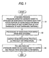
- FIG. 1 is a flowchart showing the process sequence of a method for attaching and peeling a pressure-sensitive adhesive sheet in accordance with Embodiment 1.
- a pressure-sensitive adhesive sheet formed by laminating, on a heat shrinkable material having a heat shrinkability in a uniaxial direction, a restriction layer having a property of opposing the shrinkage deformation of the heat shrinkable material and an energy-beam-curable pressure-sensitive adhesive layer in this order is attached on a semiconductor wafer.
- the pressure-sensitive adhesive sheet is attached on the semiconductor wafer so that the notch portion of the semiconductor wafer is positioned at the end in the direction of the heat shrinkage of the heat shrinkable member.
- FIG. 2 is a cross sectional view of the pressure-sensitive adhesive sheet for use in this embodiment.
- a heat shrinkable material 1 having a heat shrinkability in a uniaxial direction can be formed of a heat shrinkable film. It is essential only that the heat shrinkable film has a main shrinkage axis direction and it does not matter whether shrinkage occurs in one direction or in both longitudinal and transverse directions. Especially, for the purpose of minimizing the secondary shrinkage, a uniaxially-stretched film is preferable.
- the rate of shrinkage in the main shrinkage direction of the heat shrinkable film is, for example, 5 to 90%, and preferably 20 to 85% at a prescribed temperature in the range of 70 to 180°C (e,g., 95°C or 140°C).
- the rate of shrinkage in other directions than the main shrinkage direction of the heat shrinkable film is preferably 10% or less, further preferably 5% or less, and in particular preferably 3% or less.
- the heat shrinkable film constituting the heat shrinkable material 1 a stretched film formed with polyester, polyethylene, polypropylene, polynorbornene, polyurethane, or the like is preferable in terms of excellent coating workability of a pressure-sensitive adhesive, or the like.
- the thickness of the heat shrinkable material 1 is generally 5 to 300 ⁇ m, and preferably 10 to 100 ⁇ m.
- a restriction layer 2 is the layer for restricting the shrinkage of the heat shrinkable material 1.
- the restriction layer 2 suppresses the secondary shrinkage in different directions than the main shrinkage direction of the heat shrinkable material 1.
- the heat shrinkable material 1 is uniaxially shrinkable, the directions of shrinkage of the heat shrinkable material 1 which cannot be necessarily said to be uniform are converged into one direction. For this reason, conceivably, when a heat stimulus inducing the shrinkage of the heat shrinkable material 1 is applied to the pressure-sensitive adhesive sheet, a repulsive force in the restriction layer 2 against the shrinking force of the heat shrinkable material 1 is considered to act as a driving force.
- the outer edge portion (one edge, or opposing two edges) of the pressure-sensitive adhesive sheet lifts up, and spontaneously rolls up from the edge either in one direction or in the center direction (generally, in the main shrinkage axis direction of the heat shrinkable material) with the heat shrinkable material 1 side inward, resulting in the formation of a tubular roll.
- the restriction layer 2 can prevent the shear force generated by the shrinkage deformation of the heat shrinkable material 1 from being transmitted to a pressure-sensitive adhesive layer 3 or a wafer W.
- the restriction layer 2 has elasticity and adhesiveness (including pressure-sensitive adhesiveness) with the heat shrinkable material 1, in order to exhibit a function of restricting the shrinkage of the heat shrinkable material 1. Furthermore, the restriction layer 2 preferably has a certain degree of toughness or rigidity in order to allow the smooth formation of the tubular roll.
- the restriction layer 2 may be constituted of a single layer, or may also be constituted of a plurality of layers in which the plurality of layers share the functions.
- the restriction layer 2 is formed of, for example, an elastic layer and a rigid film layer.
- the elastic layer side is bonded onto the heat shrinkable material 1, and a pressure-sensitive adhesive layer 3 is formed on the rigid film layer side.
- the elastic layer tends to be deformed under the temperature during shrinkage of the heat shrinkable material 1, i.e., it is in a rubber state.
- the elastic layer is preferably suppressed in flowability by three dimensional crosslinking or the like.
- the elastic layer for example, there can be used a resin film (including a sheet) such as a foam material (expanded film) of urethane foam or acrylic foam, the surface (at least the surface on the heat shrinkable material 1 side) of which has been subjected to an adhesion treatment, or a non-expandable resin film using rubber, thermoplastic elastomer, or the like as a material.
- the elastic layer may also be formed with a resin composition having adhesiveness itself such as a crosslinkable acrylic pressure-sensitive adhesive.
- beads such as glass beads or resin beads may also be added. Addition of beads facilitates the control of the adhesion characteristics or the shear elastic modulus, which is advantageous.
- the rigid layer has a function of imparting the rigidity or the toughness to the restriction layer 2. Provision of the rigid layer prevents the pressure-sensitive adhesive sheet from stopping partway or deviating in direction when a heat stimulus has been applied to the heat shrinkable material 1. Thus, the pressure-sensitive adhesive sheet smoothly rolls up spontaneously to form a balanced shape tubular roll.
- the rigid film for forming the rigid layer a polyester type resin film, a polypropylene film, a polyamide film, or the like is preferred in terms of the excellent coating workability of a pressure-sensitive adhesive, or the like.
- the rigid layer may be a single layer, or a multilayer including two or more layers laminated therein.
- the film constituting the rigid layer is non-shrinkable.
- the rate of shrinkage is, for example, 5% or less, preferably 3% or less, and further preferably 1% or less.
- the thickness of the restriction layer 2 is generally 1 to 200 ⁇ m, and preferably 25 to 120 ⁇ m. When the thickness is too small, uneven coating may occur, or the interface breakage may occur due to excessive concentration of shrinkage stress. On the other hand, when the thickness of the restriction layer 2 is too large, the reduction of peelability due to excessive relaxation of shrinkage stress, or the reduction of the handling property and the cost efficiency is incurred. Thus, these cases are not preferred.
- the restriction layer 2 is formed of a resin base material layer subjected to an adhesion treatment, the overall thickness thereof preferably falls within the above-mentioned numerical value range.
- the energy-beam-curable pressure-sensitive adhesive layer 3 has a pressure-sensitive adhesiveness at the initial stage, and it is formed of a material which forms a three dimensional network structure through irradiation with an energy beam such as infrared ray, visible light, ultraviolet ray, X ray, or electron beam.
- an energy beam such as infrared ray, visible light, ultraviolet ray, X ray, or electron beam.
- a composition containing an energy-beam-curable compound incorporated in the base material (pressure-sensitive adhesive), and preferably a UV curable pressure-sensitive adhesive containing an ultraviolet (UV) curable compound incorporated in an acrylic pressure-sensitive adhesive are used.
- the thickness of the pressure-sensitive adhesive layer 3 is generally 1 to 100 ⁇ m, and preferably 10 to 60 ⁇ m.
- FIG. 3 shows the positional relationship between a semiconductor wafer W and a pressure-sensitive adhesive sheet to be attached on the surface thereof
- the semiconductor wafer W includes a notch portion N such as a V notch or an orientation flat formed therein.
- the pressure-sensitive adhesive sheet S is attached onto the semiconductor wafer W so that the notch portion N is positioned at the end in the direction of the heat shrinkage (i.e., the direction of the main shrinkage axis) H of the heat shrinkable material.
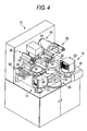
- FIG. 4 is a perspective view showing a schematic configuration of an attaching apparatus of a pressure-sensitive adhesive sheet for use in the attaching process of the step S 1.
- the attaching apparatus 10 of a pressure-sensitive adhesive sheet includes a wafer feed unit 14 (left-hand side) in which a cassette C including the wafer W stored therein is mounted, and a wafer collection unit 16 (right-hand side) for collecting the wafer W having a pressure-sensitive adhesive sheet S 1 attached on the surface thereof, on the left and right front of a base 12. Between the wafer feed unit 14 and the wafer collection unit 16, a wafer transport mechanism 20 including a robot arm 18 is disposed. Whereas, an alignment stage 22 is disposed at the right hand back of the base 12. Further, above that, a sheet feed unit 24 for feeding a pressure-sensitive adhesive sheet S 1 toward the wafer W is disposed.
- a separator collection unit 26 for collecting only separators from the pressure-sensitive adhesive sheets S 1 each with a separator thereon fed from the sheet feed unit 24 is disposed.
- a chuck table 28 for adsorbing and holding a wafer W
- a sheet attaching mechanism 30 for attaching a pressure-sensitive adhesive sheet S 1 on the wafer W held on the chuck table 28, and a sheet peeling mechanism 32 for peeling an unnecessary sheet S2 after attaching of the pressure-sensitive adhesive sheet S1 on the wafer W.
- a cutter mechanism 34 for cutting the pressure-sensitive adhesive sheet S 1 attached on the wafer W along the outer shape of the wafer W.
- the alignment stage 22 corresponds to the alignment means (alignment unit) in the attaching apparatus of a pressure-sensitive adhesive sheet in accordance with the invention.
- the cassette stage moves upward, and stops at the position at which the wafer W to be taken out can be taken out by means of the robot arm 18.
- the wafer transport mechanism 20 turns around, so that the wafer holding portion of the robot arm 18 inserts into the clearance between the wafers W in the cassette C1.
- the robot arm 18 adsorbs and holds the wafer W from the rear side on the wafer holding portion, and transfers the wafer W onto the alignment stage 22.
- the alignment of the wafer W is carried out based on the notch portion such as an orientation flat or a notch. Specifically, when the wafer W is mounted on the chuck table 28, the wafer W is aligned so that the notch portion N of the wafer W is positioned at the end in the direction of main shrinkage axis of the pressure-sensitive adhesive sheet S 1 (in this Embodiment, in the longitudinal direction of the band-like pressure-sensitive adhesive sheet S1). After alignment, the wafer W is adsorbed and held by the robot arm 5 from the rear side, and thus transferred onto the chuck table 28.
- the notch portion such as an orientation flat or a notch.
- the wafer W mounted on the chuck table 28 is adsorbed and held.
- the sheet attaching mechanism 30 and the sheet peeling mechanism 32 are positioned at the initial position on the left side, and the cutter unit 34 is positioned at the wait position on the upper side.
- an attaching roller 31 of the sheet attaching mechanism 30 moves downward in a swinging manner.
- the attaching roller 31 rotates in an opposite direction from the direction of running of the sheet (in the left to right direction in FIG. 6 ) on the wafer W while pressing the pressure-sensitive adhesive sheet S1.
- the attaching roller 31 attaches the pressure-sensitive adhesive sheet S 1 uniformly over the entire surface of the wafer W.
- the attaching roller 31 moves upward.
- the cutter mechanism 34 moves downward to the cutting action position, and the cutting edge 35 pierces and penetrates through the pressure-sensitive adhesive sheet S1.
- the cutting edge 35 stopped at a prescribed position moves along a groove not shown provided in the chuck table 28. In other words, it continues cutting the pressure-sensitive adhesive sheet S 1 along the outer shape of the wafer W.
- the cutter mechanism 34 moves upward, and returns to the wait position.
- the sheet peeling mechanism 32 rolls up and peels the unnecessary sheet S2 cut on the wafer W by means of a peel roller 33 while moving in an opposite direction from the direction of running of the sheet on the wafer W.
- the sheet peeling mechanism 32 When the sheet peeling mechanism 32 reaches the completion position of the peeling operation, the sheet peeling mechanism 32 and the sheet attaching mechanism 30 move in the direction of running of the sheet, and return to the initial position shown in FIG. 5 .
- the unnecessary sheet S2 is rolled up to the sheet collection unit 36, and a given amount of the pressure-sensitive adhesive sheet S 1 is sent out from the sheet feed unit 24. Up to this point, a round of operations for attaching the pressure-sensitive adhesive sheet S1 on the surface of the wafer W is completed.
- the process returns to FIG. 1 .
- the pressure-sensitive adhesive sheet S is attached on the semiconductor wafer W so that the notch portion N of the semiconductor wafer W is positioned at the end in the direction of main shrinkage of the pressure-sensitive adhesive sheet S.
- the process goes to the subsequent step S2.
- the rear side of the semiconductor wafer W is ground with the pressure-sensitive adhesive sheet S attached on the surface of the semiconductor wafer W.
- the semiconductor wafer W is processed to a prescribed thickness.
- the rear side of the rear-side ground semiconductor wafer W is attached to another pressure-sensitive adhesive sheet.
- the wafer W is held on a ring-like frame via the pressure-sensitive adhesive sheet.
- the process goes to the step S3 of FIG. 1 .
- the surface of the semiconductor wafer W on which the pressure-sensitive adhesive sheet S is attached is irradiated with an energy beam (an ultraviolet ray in this Embodiment) to cure the pressure-sensitive adhesive layer 3 of the pressure-sensitive adhesive sheet S (see, FIG. 9 ).
- an energy beam an ultraviolet ray in this Embodiment
- a reference sign F denotes a ring-like frame holding the wafer W via the pressure-sensitive adhesive sheet T; a reference numeral 38, a table on which the wafer W mounted on the frame F is mounted; and a reference numeral 40, an ultraviolet ray irradiation unit for irradiating the pressure-sensitive adhesive sheet S on the wafer W with an ultraviolet ray.
- the process returns to FIG. 1 .
- the process goes to the peeling process of the step S4, where the pressure-sensitive adhesive sheet S is heated and peeled off from the semiconductor wafer W.
- the wafer W mounted on the frame F is mounted on a heat plate 42 (see, FIG. 10A ).
- the pressure-sensitive adhesive sheet S attached on the wafer W is heated, so that the heat shrinkable material 1 of the pressure-sensitive adhesive sheet S shrinks in the main shrinkage axis direction.
- the pressure-sensitive adhesive layer 3 has already been cured, and pressure-sensitive adhesiveness thereof has been weakened.
- shrinkage gradient occurs in the direction vertical to the surface of the pressure-sensitive adhesive sheet S.
- the pressure-sensitive adhesive sheet S is bent in the main shrinkage axis direction to be turned up from the surface of the wafer W.
- the pressure-sensitive adhesive sheet S has been attached onto the semiconductor wafer W so that the notch portion N of the semiconductor wafer W is positioned at the end in the direction of the heat shrinkage of the heat shrinkable material. Therefore, the peripheral edge portion of the pressure-sensitive adhesive sheet S starts to be turned up from the site of the notch portion N of the semiconductor wafer W to which a stress tends to concentrate during the heat shrinkage (see, FIG. 10B ).
- the pressure-sensitive adhesive sheet S which has started to be turned up from the notch portion N of the semiconductor wafer W, as shown in FIGS 10C and 10D , freely runs while rolling up to form a tubular shape (curling in a tube) by itself in the direction away from the notch portion N, and it is thus peeled off from the surface of the wafer W.
- the pressure-sensitive adhesive sheet S starts to be peeled off from the notch portion N of the semiconductor wafer W naturally.
- it is peeled off from the wafer surface by its own shrinking force, and freely runs in a curled form. Therefore, the stress applied onto the wafer surface during peeling is very small, which can prevent the breakage of the edge of the wafer W or the cracking of the wafer W.
- Such a configuration that the pressure-sensitive adhesive sheet S attached on the semiconductor wafer W is turned up from a specific site is preferable in the case where the peeled pressure-sensitive adhesive sheet S is collected, or for automating the peeling process.
- the pressure-sensitive adhesive sheet S in the attaching process, is attached on the semiconductor wafer W so that the notch portion N of the semiconductor wafer W is positioned at the end in the direction of the heat shrinkage of the heat shrinkable material.
- the pressure-sensitive adhesive sheet S in the peeling process, the pressure-sensitive adhesive sheet S is heated after applying or while applying a mechanical force to a specific site of the peripheral edge of the pressure-sensitive adhesive sheet S attached on the semiconductor wafer W.
- the pressure-sensitive adhesive sheet S is peeled off from the site to which a mechanical force has been applied.
- the pressure-sensitive adhesive sheet S in the attaching process, it is not necessarily required that the pressure-sensitive adhesive sheet S is attached on the semiconductor wafer W so that the notch portion N of the semiconductor wafer W is positioned at the end in the direction of the heat shrinkage of the heat shrinkable material.
- the pressure-sensitive adhesive sheet S is attached in such a manner.
- the processing process of the semiconductor wafer after attaching of the pressure-sensitive adhesive sheet S (S2), and the energy irradiation process (S3) are the same as in Embodiment 1. Therefore, explanations thereon are omitted herein.
- a peel tape 46 having a pressure-sensitive adhesiveness is wound over the surface of a guide member 44.
- the peel tape 46 is brought in light contact with the specific site of the peripheral edge of the pressure-sensitive adhesive sheet S attached on the semiconductor wafer W, and then lifted. This creates turning up (cause of peeling) of the pressure-sensitive adhesive sheet S.
- the pressure-sensitive adhesive sheet S is attached on the semiconductor wafer W so that the notch portion N of the semiconductor wafer W is positioned at the end in the direction of the heat shrinkage of the heat shrinkable material. Furthermore, in the peeling process, the peel tape 46 is brought in light contact with the pressure-sensitive adhesive sheet S at the notch portion N, and then lifted. This creates the cause of peeling for the pressure-sensitive adhesive sheet S.
- a thrust member 48 like a thin pin is thrust from under the notch portion N of the semiconductor wafer W.
- the pressure-sensitive adhesive sheet S at the notch portion N is lifted. This creates the cause of peeling for the pressure-sensitive adhesive sheet S.
- an insertion member 50 like a thin pin is thrust into between the semiconductor wafer W and the pressure-sensitive adhesive sheet S.
- the specific site of the peripheral edge of the pressure-sensitive adhesive sheet S is lifted. This creates the cause of peeling for the pressure-sensitive adhesive sheet S.
- the technique for applying a mechanical force to a specific site of the peripheral edge of the pressure-sensitive adhesive sheet S can be carried out with various modifications.
- the following technique is also acceptable. From a thin nozzle, a clean gas such as compressed air or nitrogen gas is sprayed over the bonding surface between the semiconductor wafer W and the pressure-sensitive adhesive sheet S to thereby create the cause of peeling for the pressure-sensitive adhesive sheet S.
- the cause of peeling of the pressure-sensitive adhesive sheet S can also be implemented by heating the pressure-sensitive adhesive sheet S with a temperature gradient given thereto, other than the techniques of Embodiments 1 and 2 described above.
- the pressure-sensitive adhesive sheet S is heated with a temperature gradient given thereto, the pressure-sensitive adhesive sheet S starts to be turned up from a site at which the heat shrinkage deformation is largest and the temperature is highest.
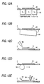
- FIGS. 12A to 12E a description will be given to an example of the constitution for heating the pressure-sensitive adhesive sheet S with a temperature gradient given thereto (heating units).
- the processing process of the semiconductor wafer after attaching of the pressure-sensitive adhesive sheet S (S2), and the energy irradiation process (S3) are the same as in Embodiment 1. Therefore, explanations thereon are omitted herein.
- the temperatures T 1 , T 2 , and T 3 of the heat plate 52 are set to satisfy the following relationship: T 1 > T 2 > T 3 . Therefore, the pressure-sensitive adhesive sheet S starts to be peeled off from the site set at the highest temperature T1.
- the heat plate 54 having an uniform temperature distribution is brought in contact with the rear side of the wafer W at shifted timings, whereby the temperature gradient in the pressure-sensitive adhesive sheet S is generated. This creates the cause of peeling of the pressure-sensitive adhesive sheet S at the site with which the heat plate 54 has early come in contact.
- warm air is sprayed toward a specific site of the peripheral edge of the wafer W from a nozzle 56, and then the nozzle 56 is moved in one direction so that warm air is sprayed over the entire wafer W, whereby the temperature gradient in the wafer W is generated. This creates the cause of peeling of the pressure-sensitive adhesive sheet S at the site to which warm air has been early sprayed.
- a roller 58 including a heater therein is brought in contact with the rear side of the wafer W and rotated in one direction, whereby the temperature gradient in the wafer W is generated. This creates the cause of peeling of the pressure-sensitive adhesive sheet S at the site with which the roller has come in contact first.
- a peel bar 59 including a heater therein is horizontally moved to attach the peel tape 46 on the self-adhesive tape S, whereby the temperature gradient in the wafer W is generated. This creates the cause of peeling of the pressure-sensitive adhesive sheet S at the outer peripheral part of the wafer.
- the technique for heating the pressure-sensitive adhesive sheet S with a temperature gradient given thereto can be carried out with various modifications.
- the following technique is also acceptable.
- a slit-like infrared ray is exposed from the surface side of the semiconductor wafer W and is allowed to scan in one direction along the wafer surface. This results in the occurrence of the temperature gradient in the semiconductor wafer W.
- the pressure-sensitive adhesive sheet S has a property of freely running in one direction over the wafer surface while spirally rolls up to form a tubular shape by heating of the pressure-sensitive adhesive sheet S. Therefore, the peeled pressure-sensitive adhesive sheets S can be collected with ease by various techniques.
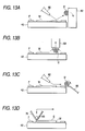
- a clean gas such as compressed air or nitrogen gas is sprayed from a nozzle 60.
- a tubular body S' of the rolled-up pressure-sensitive adhesive sheet is charged and collected into a collection container (duster shoot) 62.
- the pressure-sensitive adhesive sheet S which has been freely running in one direction over the wafer surface while spirally rolls up to form a tubular shape, is sucked by a suction duct 64, and collected.
- a clean gas such as compressed air or nitrogen gas is sprayed from the nozzle 60.
- the tubular body S' of the pressure-sensitive adhesive sheet is rotated along a guide path 66, and collected.
- a peel tape 70 having pressure-sensitive adhesiveness is wound over the surface of a collection roll 68.
- the peel tape 70 is brought in light contact with the specific site of the peripheral edge of the pressure-sensitive adhesive sheet S attached on the semiconductor wafer W, and lifted. Subsequently, while horizontally moving the collection roll 68, peeling of the pressure-sensitive adhesive sheet S from the wafer W is promoted. Thus, the pressure-sensitive adhesive sheet S is collected together with the peel tape 70.
- the pressure-sensitive adhesive sheet S which has been freely running in one direction over the wafer surface while spirally rolls up to form a tubular shape, is stopped by a member 72 at one end of the wafer W.
- the stopped tubular body S' of the pressure-sensitive adhesive sheet is held by a collecting pressure-sensitive adhesive tape 76 wound over a guide roll 74.
- the tubular body S' of the pressure-sensitive adhesive sheet is collected together with the collecting pressure-sensitive adhesive tape 76.
- the pressure-sensitive adhesive sheet S which has been freely running in one direction over the wafer surface while spirally rolls up to form a tubular shape, is stopped by the member 72 at one end of the wafer W.
- the stopped tubular body S' of the pressure-sensitive adhesive sheet is held by the use of a robot arm 78, and collected.
- the cause of peeling is created at a specific site of the peripheral edge of the wafer W.
- the site is brought in light contact with the collecting pressure-sensitive adhesive tape 76, and lifted.
- peeling of the pressure-sensitive adhesive sheet S from the wafer W is promoted.
- the pressure-sensitive adhesive sheet S is collected together with the peel tape 70.
- a strip-like interleaf 80 is placed on the wafer W with the pressure-sensitive adhesive sheet S attached thereon.
- the heated pressure-sensitive adhesive sheet S freely runs in one direction over the wafer surface while spirally enwinding the interleaf 80 to form a tubular shape.
- one end of the interleaf 80 extending off the tubular body S' is held, so that the pressure-sensitive adhesive sheet S is collected together with the interleaf 80.
- the constitution for collecting the pressure-sensitive adhesive sheet S can be carried out with various modifications, and is not limited to the foregoing examples.
Landscapes
- Container, Conveyance, Adherence, Positioning, Of Wafer (AREA)
- Mechanical Treatment Of Semiconductor (AREA)
- Adhesive Tapes (AREA)
- Adhesives Or Adhesive Processes (AREA)
Abstract

Description
- The present invention relates to a method for attaching and peeling a pressure-sensitive adhesive sheet onto or from a semiconductor wafer, and an attaching apparatus of a pressure-sensitive adhesive sheet and a peeling apparatus of a pressure-sensitive adhesive sheet. More particularly, it relates to a technology of attaching and peeling a pressure-sensitive adhesive sheet having heat shrinkability.
- In recent years, a semiconductor wafer has been increased in size to a diameter of about 300 mm. On the contrary, it has been gradually decreased in thickness to 100 µm or smaller. A large and thin semiconductor wafer is very likely to be broken. Therefore, prior to grinding processing of the rear side of the wafer, a pressure-sensitive adhesive sheet for surface protection and reinforcement is attached on the wafer surface to hold the wafer, and after performing rear side grinding, the pressure-sensitive adhesive sheet is peeled off and collected from the wafer.
- The pressure-sensitive adhesive sheet attached on the wafer surface generally includes an energy beam (e.g., ultraviolet ray) curable pressure-sensitive adhesive layer formed therein. The pressure-sensitive adhesive sheet is attached onto a wafer, and temporarily fixed thereon. The resulting wafer is subsequently subjected to a grinding processing, and it is then irradiated with an energy beam to cure the pressure-sensitive adhesive layer. Thus, the pressure-sensitive adhesive sheet which has been reduced in adhesion is peeled off from the wafer. However, the pressure-sensitive adhesive sheet which has been reduced in adhesion through energy beam irradiation still adheres to the wafer surface under air pressure. This necessitates the following operation in order to peel the pressure-sensitive adhesive sheet from the wafer. A release sheet is further attached on the pressure-sensitive adhesive sheet. Then, the pressure-sensitive adhesive sheet is turned up from the wafer integrally with the release sheet. During such a peeling operation, unfavorably, an excessive force acts on the wafer, so that the end of the wafer is broken, or the wafer is cracked.
- Under such circumstances, there have been proposed techniques each using a pressure-sensitive adhesive sheet including an energy-beam-curable pressure-sensitive adhesive layer and a heat shrinkable film in the layer structure thereof (e.g.,
JP-A-2003- 261842 JP-A-2000-129227 JP-A-2001-72327 JP-A-2001-7179 - However, with a conventional technique using a pressure-sensitive adhesive sheet, since the shrinkage of a heat shrinkable film occurs from a plurality of directions, there arises a problem that the pressure-sensitive adhesive sheet after heating is folded one part over another on the wafer surface, whereby the peeling unfavorably becomes difficult. Further, in general, even for the products commercially available as a uniaxially shrinkable film secondary shrinkage unfavorably occurs in different axial directions due to the residual stress upon production, or due to the stress or the heat distortion applied to the pressure-sensitive adhesive sheet during the manufacturing process, or the like. Especially when a pressure-sensitive adhesive sheet is attached onto a large semiconductor wafer, the secondary shrinkage also increases, which inhibits the shrinkage in the main shrinkage axis direction, whereby the pressure-sensitive adhesive sheet tends to be difficult to be peeled off. As a result, after peeling, a part of the pressure-sensitive adhesive sheet adheres to the wafer and remains thereon; the semiconductor wafer is broken by an nonuniform stress upon shrinkage; the cured pressure-sensitive adhesive falls off from the pressure-sensitive adhesive sheet to contaminate the wafer; or other problems occur.
- In view of such circumstances, the present invention has been accomplished. It is therefore an object of the invention to provide a method for attaching and peeling a pressure-sensitive adhesive sheet capable of readily peeling off the pressure-sensitive adhesive sheet attached onto a semiconductor wafer by heating; and an attaching apparatus of a pressure-sensitive adhesive sheet, and a peeling apparatus of a pressure-sensitive adhesive sheet.
-
-
FIG. 1 shows a flowchart showing the step sequence of a method for attaching and peeling a pressure-sensitive adhesive sheet in accordance withEmbodiment 1 of the present invention. -
FIG. 2 shows a cross sectional view of the pressure-sensitive adhesive sheet for use inEmbodiment 1. -
FIG. 3 shows a view showing the positional relationship between a semiconductor wafer W and a pressure-sensitive adhesive sheet to be attached on the surface thereof -
FIG. 4 shows a perspective view showing a schematic configuration of an attaching apparatus of a pressure-sensitive adhesive sheet for use in an attaching process ofEmbodiment 1. -
FIG. 5 shows an explanatory view of the operation of an attaching apparatus of a pressure-sensitive adhesive sheet in accordance withEmbodiment 1. -
FIG. 6 shows an explanatory view of the operation of an attaching apparatus of a pressure-sensitive adhesive sheet in accordance withEmbodiment 1. -
FIG. 7 shows an explanatory view of the operation of an attaching apparatus of a pressure-sensitive adhesive sheet in accordance withEmbodiment 1. -
FIG. 8 shows an explanatory view of the operation of an attaching apparatus of a pressure-sensitive adhesive sheet in accordance withEmbodiment 1. -
FIG. 9 shows an explanatory view of an energy beam irradiation process ofEmbodiment 1. -
FIGS. 10A to 10D show views for illustrating a peeling process ofEmbodiment 1. -
FIGS. 11A to 11D show views for illustrating an example of a configuration of a peeling process ofEmbodiment 2. -
FIGS. 12A to 12E show views for illustrating an example of a configuration of a peeling process ofEmbodiment 3. -
FIGS. 13A to 13D show views for illustrating an example of a configuration for adhesive-sheet collection in Embodiment 4. -
FIGS. 14E to 14H show views for illustrating an example of a configuration for adhesive-sheet collection in Embodiment 4. -
- W
- Semiconductor wafer
- S
- Pressure-sensitive adhesive sheet
- S'
- Tubular body of pressure-sensitive adhesive sheet
- 1
- Heat shrinkable material
- 2
- Restriction layer
- 3
- Pressure-sensitive adhesive layer
- In order to attain such an object, the present invention provides the following (1) to (8).
- (1) A method for attaching and peeling a pressure-sensitive adhesive sheet comprising:
- attaching on a semiconductor wafer a pressure-sensitive adhesive sheet comprising a heat shrinkable material having a heat shrinkability in at least a uniaxial direction, a restriction layer having a property of opposing a shrinkage deformation of the heat shrinkable material, and an energy-beam-curable pressure-sensitive adhesive layer laminated in this order;
- subjecting the semiconductor wafer on which the pressure-sensitive adhesive sheet is attached to a predetermined treatment, followed by irradiating the semiconductor wafer with an energy beam to thereby cure the pressure-sensitive adhesive layer; and
- heating the pressure-sensitive adhesive sheet after said curing of the pressure-sensitive adhesive layer to thereby peeling off the pressure-sensitive adhesive sheet from the semiconductor wafer,
- (2) A method for attaching and peeling a pressure-sensitive adhesive sheet comprising:
- attaching on a semiconductor wafer a pressure-sensitive adhesive sheet comprising a heat shrinkable material having a heat shrinkability in at least a uniaxial direction, a restriction layer having a property of opposing a shrinkage deformation of the heat shrinkable material, and an energy-beam-curable pressure-sensitive adhesive layer laminated in this order;
- subjecting the semiconductor wafer on which the pressure-sensitive adhesive sheet is attached to a predetermined treatment, followed by irradiating the semiconductor wafer with an energy beam to thereby cure the pressure-sensitive adhesive layer; and
- heating the pressure-sensitive adhesive sheet after said curing of the pressure-sensitive adhesive layer to thereby peeling off the pressure-sensitive adhesive sheet from the semiconductor wafer,
- (3) A method for attaching and peeling a pressure-sensitive adhesive sheet comprising:
- attaching on a semiconductor wafer a pressure-sensitive adhesive sheet comprising a heat shrinkable material having a heat shrinkability in at least a uniaxial direction, a restriction layer having a property of opposing a shrinkage deformation of the heat shrinkable material, and an energy-beam-curable pressure-sensitive adhesive layer laminated in this order;
- subjecting the semiconductor wafer on which the pressure-sensitive adhesive sheet is attached to a predetermined treatment, followed by irradiating the semiconductor wafer with an energy beam to thereby cure the pressure-sensitive adhesive layer; and
- heating the pressure-sensitive adhesive sheet after said curing of the pressure-sensitive adhesive layer to thereby peeling off the pressure-sensitive adhesive sheet from the semiconductor wafer,
- (4) An attaching apparatus of a pressure-sensitive adhesive sheet for carrying out said attaching in the method according to (1) above,
the apparatus comprising an alignment unit which adjust the positional relationship between the pressure-sensitive adhesive sheet and the semiconductor wafer such that the notch portion of the semiconductor wafer is positioned at the end in the direction of the heat shrinkage of the heat shrinkable material. - (5) A peeling apparatus of a pressure-sensitive adhesive sheet for carrying out said peeling in the method according to (2) above,
the apparatus comprising a mechanical force applying unit which applies a mechanical force to a specific site of the peripheral edge of the pressure-sensitive adhesive sheet attached on the semiconductor wafer. - (6) A peeling apparatus of a pressure-sensitive adhesive sheet for carrying out said peeling in the method according to (3) above,
the apparatus comprising a heating unit which heats the pressure-sensitive adhesive sheet with a temperature gradient given thereto. - (7) The peeling apparatus of a pressure-sensitive adhesive sheet according to (5),
the apparatus comprising a collection unit which collects the pressure-sensitive adhesive sheet having been peeled off from the semiconductor wafer to form a tubular shape by said heating. - (8) The peeling apparatus of a pressure-sensitive adhesive sheet according to (6),
the apparatus comprising a collection unit which collects the pressure-sensitive adhesive sheet having been peeled off from the semiconductor wafer to form a tubular shape by said heating. - In accordance with (1) above, by providing a restriction layer having a property of opposing the shrinkage deformation of a heat shrinkable material between the heat shrinkable material and an energy-beam-curable pressure-sensitive adhesive layer, shrinkage gradient occurs in the direction vertical to the surface of the pressure-sensitive adhesive sheet upon shrinking the heat shrinkable material by heating. As a result, the outer edge portion of the pressure-sensitive adhesive sheet rises from the surface of the semiconductor wafer, and is peeled off while spontaneously rolling up in one direction to form a tube shape. This can circumvent a problem of breakage of the semiconductor wafer by a stress upon peeling, contamination of the semiconductor wafer by incomplete peeling, or the like. Thus, it is possible to peel the pressure-sensitive adhesive sheet with ease. Whereas, in the attaching process, the pressure-sensitive adhesive sheet is attached on the semiconductor wafer such that a notch portion of the semiconductor wafer is positioned at the end in the direction of the heat shrinkage of the heat shrinkable material. Therefore, the outer edge portion of the pressure-sensitive adhesive sheet starts to be turned up from the notch portion of the semiconductor wafer to which a stress tends to concentrate during the heat shrinkage. In other words, since the pressure-sensitive adhesive sheet starts to be peeled off from the notch portion of the semiconductor wafer naturally, the stress during peeling can be further decreased.
- In accordance with (2) above, in the peeling process, the pressure-sensitive adhesive sheet is heated to be peeled off from the semiconductor wafer after applying or while applying a mechanical force to a specific site of the peripheral edge of the pressure-sensitive adhesive sheet attached on the semiconductor wafer. Accordingly, the outer edge portion of the pressure-sensitive adhesive sheet starts to be turned up from the specific site to which a mechanical force has been applied. In other words, since the pressure-sensitive adhesive sheet starts to be naturally peeled off from a specific site of the peripheral edge of the pressure-sensitive adhesive sheet, the stress during peeling can be further decreased.
- In accordance with (3) above, in the peeling process, the pressure-sensitive adhesive sheet is heated with a temperature gradient given thereto, and then peeled off from the semiconductor wafer. Accordingly, the pressure-sensitive adhesive sheet starts to be turned up from a site at which the heat shrinkage deformation is largest and the temperature is highest. In other words, since the pressure-sensitive adhesive sheet starts to be naturally peeled off from a specific site of the peripheral edge of the pressure-sensitive adhesive sheet, the stress during peeling can be further decreased.
- In accordance with (4) above, it is possible to preferably carry out the method for attaching and peeling a pressure-sensitive adhesive sheet according to (1) above.
- In accordance with (5) above, it is possible to preferably carry out the method for attaching and peeling a pressure-sensitive adhesive sheet according to (2) above.
- In accordance with (6) above, it is possible to preferably carry out the method for attaching and peeling a pressure-sensitive adhesive sheet according to (3) above.
- In accordance with (7) and (8) above, the apparatus includes a collection unit which collects a pressure-sensitive adhesive sheet having been peeled off from the semiconductor wafer to form a tubular shape. Therefore, the peeled pressure-sensitive adhesive sheet does not obstruct the subsequent peeling process, which allows continuous smooth peeling of pressure-sensitive adhesive sheets.
- According to the methods for attaching and peeling a pressure-sensitive adhesive sheet in accordance with the invention, when a heat shrinkable material is shrinked by heating, the pressure-sensitive adhesive sheet rises from a specific site of the peripheral edge of the pressure-sensitive adhesive sheet, and is peeled while spontaneously rolling up in one direction to form a tubular shape. This can circumvent a problem of breakage of the semiconductor wafer by a stress upon peeling, contamination of the semiconductor wafer by incomplete peeling, or the like. Thus, it is possible to peel off the pressure-sensitive adhesive sheet with ease. Furthermore, according to the attaching apparatus of a pressure-sensitive adhesive sheet and the peeling apparatus of a pressure-sensitive adhesive sheet in accordance with the invention, it is possible to preferably carry out the method for attaching and peeling a pressure-sensitive adhesive sheet in accordance with the invention.
- In the followings,
Embodiment 1 of the invention will be described by reference to the accompanying drawings. -
FIG. 1 is a flowchart showing the process sequence of a method for attaching and peeling a pressure-sensitive adhesive sheet in accordance withEmbodiment 1. - First, in an attaching process of a step S1, a pressure-sensitive adhesive sheet formed by laminating, on a heat shrinkable material having a heat shrinkability in a uniaxial direction, a restriction layer having a property of opposing the shrinkage deformation of the heat shrinkable material and an energy-beam-curable pressure-sensitive adhesive layer in this order, is attached on a semiconductor wafer. At this step, the pressure-sensitive adhesive sheet is attached on the semiconductor wafer so that the notch portion of the semiconductor wafer is positioned at the end in the direction of the heat shrinkage of the heat shrinkable member.
-
FIG. 2 is a cross sectional view of the pressure-sensitive adhesive sheet for use in this embodiment. - A
heat shrinkable material 1 having a heat shrinkability in a uniaxial direction can be formed of a heat shrinkable film. It is essential only that the heat shrinkable film has a main shrinkage axis direction and it does not matter whether shrinkage occurs in one direction or in both longitudinal and transverse directions. Especially, for the purpose of minimizing the secondary shrinkage, a uniaxially-stretched film is preferable. The rate of shrinkage in the main shrinkage direction of the heat shrinkable film is, for example, 5 to 90%, and preferably 20 to 85% at a prescribed temperature in the range of 70 to 180°C (e,g., 95°C or 140°C). The rate of shrinkage in other directions than the main shrinkage direction of the heat shrinkable film is preferably 10% or less, further preferably 5% or less, and in particular preferably 3% or less. As the heat shrinkable film constituting theheat shrinkable material 1, a stretched film formed with polyester, polyethylene, polypropylene, polynorbornene, polyurethane, or the like is preferable in terms of excellent coating workability of a pressure-sensitive adhesive, or the like. The thickness of theheat shrinkable material 1 is generally 5 to 300 µm, and preferably 10 to 100 µm. - A
restriction layer 2 is the layer for restricting the shrinkage of theheat shrinkable material 1. Therestriction layer 2 suppresses the secondary shrinkage in different directions than the main shrinkage direction of theheat shrinkable material 1. Though theheat shrinkable material 1 is uniaxially shrinkable, the directions of shrinkage of theheat shrinkable material 1 which cannot be necessarily said to be uniform are converged into one direction. For this reason, conceivably, when a heat stimulus inducing the shrinkage of theheat shrinkable material 1 is applied to the pressure-sensitive adhesive sheet, a repulsive force in therestriction layer 2 against the shrinking force of theheat shrinkable material 1 is considered to act as a driving force. Thus, the outer edge portion (one edge, or opposing two edges) of the pressure-sensitive adhesive sheet lifts up, and spontaneously rolls up from the edge either in one direction or in the center direction (generally, in the main shrinkage axis direction of the heat shrinkable material) with theheat shrinkable material 1 side inward, resulting in the formation of a tubular roll. Furthermore, therestriction layer 2 can prevent the shear force generated by the shrinkage deformation of theheat shrinkable material 1 from being transmitted to a pressure-sensitive adhesive layer 3 or a wafer W. This can prevent breakage of the pressure-sensitive adhesive layer which has been reduced in adhesion strength upon repeeling (e.g., a cured pressure-sensitive adhesive layer), breakage of the wafer, contamination of the wafer by the broken pressure-sensitive adhesive layer, or the like. - The
restriction layer 2 has elasticity and adhesiveness (including pressure-sensitive adhesiveness) with theheat shrinkable material 1, in order to exhibit a function of restricting the shrinkage of theheat shrinkable material 1. Furthermore, therestriction layer 2 preferably has a certain degree of toughness or rigidity in order to allow the smooth formation of the tubular roll. Therestriction layer 2 may be constituted of a single layer, or may also be constituted of a plurality of layers in which the plurality of layers share the functions. - The
restriction layer 2 is formed of, for example, an elastic layer and a rigid film layer. The elastic layer side is bonded onto theheat shrinkable material 1, and a pressure-sensitive adhesive layer 3 is formed on the rigid film layer side. Preferably, the elastic layer tends to be deformed under the temperature during shrinkage of theheat shrinkable material 1, i.e., it is in a rubber state. The elastic layer is preferably suppressed in flowability by three dimensional crosslinking or the like. For the elastic layer, for example, there can be used a resin film (including a sheet) such as a foam material (expanded film) of urethane foam or acrylic foam, the surface (at least the surface on theheat shrinkable material 1 side) of which has been subjected to an adhesion treatment, or a non-expandable resin film using rubber, thermoplastic elastomer, or the like as a material. Additionally, the elastic layer may also be formed with a resin composition having adhesiveness itself such as a crosslinkable acrylic pressure-sensitive adhesive. To the constituent components of the elastic layer, beads such as glass beads or resin beads may also be added. Addition of beads facilitates the control of the adhesion characteristics or the shear elastic modulus, which is advantageous. - The rigid layer has a function of imparting the rigidity or the toughness to the
restriction layer 2. Provision of the rigid layer prevents the pressure-sensitive adhesive sheet from stopping partway or deviating in direction when a heat stimulus has been applied to theheat shrinkable material 1. Thus, the pressure-sensitive adhesive sheet smoothly rolls up spontaneously to form a balanced shape tubular roll. As the rigid film for forming the rigid layer, a polyester type resin film, a polypropylene film, a polyamide film, or the like is preferred in terms of the excellent coating workability of a pressure-sensitive adhesive, or the like. The rigid layer may be a single layer, or a multilayer including two or more layers laminated therein. The film constituting the rigid layer is non-shrinkable. The rate of shrinkage is, for example, 5% or less, preferably 3% or less, and further preferably 1% or less. - The thickness of the
restriction layer 2 is generally 1 to 200 µm, and preferably 25 to 120 µm. When the thickness is too small, uneven coating may occur, or the interface breakage may occur due to excessive concentration of shrinkage stress. On the other hand, when the thickness of therestriction layer 2 is too large, the reduction of peelability due to excessive relaxation of shrinkage stress, or the reduction of the handling property and the cost efficiency is incurred. Thus, these cases are not preferred. Incidentally, when therestriction layer 2 is formed of a resin base material layer subjected to an adhesion treatment, the overall thickness thereof preferably falls within the above-mentioned numerical value range. - The energy-beam-curable pressure-
sensitive adhesive layer 3 has a pressure-sensitive adhesiveness at the initial stage, and it is formed of a material which forms a three dimensional network structure through irradiation with an energy beam such as infrared ray, visible light, ultraviolet ray, X ray, or electron beam. Specifically, for example, a composition containing an energy-beam-curable compound incorporated in the base material (pressure-sensitive adhesive), and preferably a UV curable pressure-sensitive adhesive containing an ultraviolet (UV) curable compound incorporated in an acrylic pressure-sensitive adhesive are used. The thickness of the pressure-sensitive adhesive layer 3 is generally 1 to 100 µm, and preferably 10 to 60 µm. When the thickness is too small, it becomes impossible to absorb the unevenness of the wafer pattern or it becomes difficult to hold or temporarily fix the semiconductor wafer, which may incur breakage of the wafer. On the other hand, a too large thickness of the pressure-sensitive adhesive layer 3 is uneconomical, and results in inferior handling property, and hence it is not preferable. -
FIG. 3 shows the positional relationship between a semiconductor wafer W and a pressure-sensitive adhesive sheet to be attached on the surface thereof In general, the semiconductor wafer W includes a notch portion N such as a V notch or an orientation flat formed therein. In thisEmbodiment 1, the pressure-sensitive adhesive sheet S is attached onto the semiconductor wafer W so that the notch portion N is positioned at the end in the direction of the heat shrinkage (i.e., the direction of the main shrinkage axis) H of the heat shrinkable material. -
FIG. 4 is a perspective view showing a schematic configuration of an attaching apparatus of a pressure-sensitive adhesive sheet for use in the attaching process of thestep S 1. - The attaching
apparatus 10 of a pressure-sensitive adhesive sheet includes a wafer feed unit 14 (left-hand side) in which a cassette C including the wafer W stored therein is mounted, and a wafer collection unit 16 (right-hand side) for collecting the wafer W having a pressure-sensitiveadhesive sheet S 1 attached on the surface thereof, on the left and right front of abase 12. Between thewafer feed unit 14 and thewafer collection unit 16, awafer transport mechanism 20 including arobot arm 18 is disposed. Whereas, analignment stage 22 is disposed at the right hand back of thebase 12. Further, above that, asheet feed unit 24 for feeding a pressure-sensitiveadhesive sheet S 1 toward the wafer W is disposed. Whereas, on the right side diagonally under thesheet feed unit 24, aseparator collection unit 26 for collecting only separators from the pressure-sensitiveadhesive sheets S 1 each with a separator thereon fed from thesheet feed unit 24 is disposed. On the left side of thealignment stage 22, there are disposed a chuck table 28 for adsorbing and holding a wafer W, asheet attaching mechanism 30 for attaching a pressure-sensitiveadhesive sheet S 1 on the wafer W held on the chuck table 28, and asheet peeling mechanism 32 for peeling an unnecessary sheet S2 after attaching of the pressure-sensitive adhesive sheet S1 on the wafer W. Above that, acutter mechanism 34 for cutting the pressure-sensitiveadhesive sheet S 1 attached on the wafer W along the outer shape of the wafer W. Further, on the left side above thebase 12, asheet collection unit 36 for collecting unnecessary sheets is disposed. Incidentally, thealignment stage 22 corresponds to the alignment means (alignment unit) in the attaching apparatus of a pressure-sensitive adhesive sheet in accordance with the invention. - Then, the operation of the attaching
apparatus 10 will be described. - When the cassette C1 including wafers W stored in multistage therein is mounted on the cassette stage of the
wafer feed unit 14, the cassette stage moves upward, and stops at the position at which the wafer W to be taken out can be taken out by means of therobot arm 18. - The
wafer transport mechanism 20 turns around, so that the wafer holding portion of therobot arm 18 inserts into the clearance between the wafers W in the cassette C1. Therobot arm 18 adsorbs and holds the wafer W from the rear side on the wafer holding portion, and transfers the wafer W onto thealignment stage 22. - For the wafer W mounted on the
alignment stage 22, the alignment of the wafer W is carried out based on the notch portion such as an orientation flat or a notch. Specifically, when the wafer W is mounted on the chuck table 28, the wafer W is aligned so that the notch portion N of the wafer W is positioned at the end in the direction of main shrinkage axis of the pressure-sensitive adhesive sheet S 1 (in this Embodiment, in the longitudinal direction of the band-like pressure-sensitive adhesive sheet S1). After alignment, the wafer W is adsorbed and held by the robot arm 5 from the rear side, and thus transferred onto the chuck table 28. - The wafer W mounted on the chuck table 28 is adsorbed and held. At this step, as shown in
FIG. 5 , thesheet attaching mechanism 30 and thesheet peeling mechanism 32 are positioned at the initial position on the left side, and thecutter unit 34 is positioned at the wait position on the upper side. - When the wafer W is adsorbed and held, as shown in
FIG. 6 , an attachingroller 31 of thesheet attaching mechanism 30 moves downward in a swinging manner. Thus, the attachingroller 31 rotates in an opposite direction from the direction of running of the sheet (in the left to right direction inFIG. 6 ) on the wafer W while pressing the pressure-sensitive adhesive sheet S1. As a result, it attaches the pressure-sensitiveadhesive sheet S 1 uniformly over the entire surface of the wafer W. When thesheet attaching mechanism 30 reaches the completion position, the attachingroller 31 moves upward. - Then, as shown in
FIG. 7 , thecutter mechanism 34 moves downward to the cutting action position, and thecutting edge 35 pierces and penetrates through the pressure-sensitive adhesive sheet S1. Thecutting edge 35 stopped at a prescribed position moves along a groove not shown provided in the chuck table 28. In other words, it continues cutting the pressure-sensitiveadhesive sheet S 1 along the outer shape of the wafer W. - After cutting the pressure-sensitive adhesive sheet S1, as shown in
FIG. 8 , thecutter mechanism 34 moves upward, and returns to the wait position. - Then, as shown in
FIG. 8 , thesheet peeling mechanism 32 rolls up and peels the unnecessary sheet S2 cut on the wafer W by means of apeel roller 33 while moving in an opposite direction from the direction of running of the sheet on the wafer W. - When the
sheet peeling mechanism 32 reaches the completion position of the peeling operation, thesheet peeling mechanism 32 and thesheet attaching mechanism 30 move in the direction of running of the sheet, and return to the initial position shown inFIG. 5 . At this step, the unnecessary sheet S2 is rolled up to thesheet collection unit 36, and a given amount of the pressure-sensitiveadhesive sheet S 1 is sent out from thesheet feed unit 24. Up to this point, a round of operations for attaching the pressure-sensitive adhesive sheet S1 on the surface of the wafer W is completed. - The process returns to
FIG. 1 . In the foregoing manner, the pressure-sensitive adhesive sheet S is attached on the semiconductor wafer W so that the notch portion N of the semiconductor wafer W is positioned at the end in the direction of main shrinkage of the pressure-sensitive adhesive sheet S. Then, the process goes to the subsequent step S2. At this step, the rear side of the semiconductor wafer W is ground with the pressure-sensitive adhesive sheet S attached on the surface of the semiconductor wafer W. Thus, the semiconductor wafer W is processed to a prescribed thickness. - The rear side of the rear-side ground semiconductor wafer W is attached to another pressure-sensitive adhesive sheet. Thus, the wafer W is held on a ring-like frame via the pressure-sensitive adhesive sheet. Then, the process goes to the step S3 of
FIG. 1 . The surface of the semiconductor wafer W on which the pressure-sensitive adhesive sheet S is attached is irradiated with an energy beam (an ultraviolet ray in this Embodiment) to cure the pressure-sensitive adhesive layer 3 of the pressure-sensitive adhesive sheet S (see,FIG. 9 ). Incidentally, inFIG. 9 , a reference sign F denotes a ring-like frame holding the wafer W via the pressure-sensitive adhesive sheet T; areference numeral 38, a table on which the wafer W mounted on the frame F is mounted; and areference numeral 40, an ultraviolet ray irradiation unit for irradiating the pressure-sensitive adhesive sheet S on the wafer W with an ultraviolet ray. - The process returns to
FIG. 1 . When the energy-beam-irradiation process (S3) is completed, the process goes to the peeling process of the step S4, where the pressure-sensitive adhesive sheet S is heated and peeled off from the semiconductor wafer W. Specifically, as shown inFIGS. 10A to 10D , the wafer W mounted on the frame F is mounted on a heat plate 42 (see,FIG. 10A ). As a result, the pressure-sensitive adhesive sheet S attached on the wafer W is heated, so that theheat shrinkable material 1 of the pressure-sensitive adhesive sheet S shrinks in the main shrinkage axis direction. At this step, the pressure-sensitive adhesive layer 3 has already been cured, and pressure-sensitive adhesiveness thereof has been weakened. Then, in theheat shrinkable material 1, and therestriction layer 2 interposed between it and the cured pressure-sensitive adhesive layer 3, shrinkage gradient occurs in the direction vertical to the surface of the pressure-sensitive adhesive sheet S. As a result, the pressure-sensitive adhesive sheet S is bent in the main shrinkage axis direction to be turned up from the surface of the wafer W. - In the attaching process, the pressure-sensitive adhesive sheet S has been attached onto the semiconductor wafer W so that the notch portion N of the semiconductor wafer W is positioned at the end in the direction of the heat shrinkage of the heat shrinkable material. Therefore, the peripheral edge portion of the pressure-sensitive adhesive sheet S starts to be turned up from the site of the notch portion N of the semiconductor wafer W to which a stress tends to concentrate during the heat shrinkage (see,
FIG. 10B ). - The pressure-sensitive adhesive sheet S which has started to be turned up from the notch portion N of the semiconductor wafer W, as shown in
FIGS 10C and 10D , freely runs while rolling up to form a tubular shape (curling in a tube) by itself in the direction away from the notch portion N, and it is thus peeled off from the surface of the wafer W. Thus, the pressure-sensitive adhesive sheet S starts to be peeled off from the notch portion N of the semiconductor wafer W naturally. Thus, it is peeled off from the wafer surface by its own shrinking force, and freely runs in a curled form. Therefore, the stress applied onto the wafer surface during peeling is very small, which can prevent the breakage of the edge of the wafer W or the cracking of the wafer W. - Such a configuration that the pressure-sensitive adhesive sheet S attached on the semiconductor wafer W is turned up from a specific site is preferable in the case where the peeled pressure-sensitive adhesive sheet S is collected, or for automating the peeling process. For that purpose, in
Embodiment 1, in the attaching process, the pressure-sensitive adhesive sheet S is attached on the semiconductor wafer W so that the notch portion N of the semiconductor wafer W is positioned at the end in the direction of the heat shrinkage of the heat shrinkable material. In contrast, inEmbodiment 2, in the peeling process, the pressure-sensitive adhesive sheet S is heated after applying or while applying a mechanical force to a specific site of the peripheral edge of the pressure-sensitive adhesive sheet S attached on the semiconductor wafer W. As a result, the pressure-sensitive adhesive sheet S is peeled off from the site to which a mechanical force has been applied. In the case of this Embodiment, in the attaching process, it is not necessarily required that the pressure-sensitive adhesive sheet S is attached on the semiconductor wafer W so that the notch portion N of the semiconductor wafer W is positioned at the end in the direction of the heat shrinkage of the heat shrinkable material. However, it is also acceptable that the pressure-sensitive adhesive sheet S is attached in such a manner. Incidentally, the processing process of the semiconductor wafer after attaching of the pressure-sensitive adhesive sheet S (S2), and the energy irradiation process (S3) are the same as inEmbodiment 1. Therefore, explanations thereon are omitted herein. - In the followings, by reference to
FIGS. 11A to 11D , a description will be given to the constitution for applying a mechanical force to a specific site of the peripheral edge of the pressure-sensitive adhesive sheet S (mechanical force applying unit). - By reference to
FIG. 11A , apeel tape 46 having a pressure-sensitive adhesiveness is wound over the surface of aguide member 44. Thepeel tape 46 is brought in light contact with the specific site of the peripheral edge of the pressure-sensitive adhesive sheet S attached on the semiconductor wafer W, and then lifted. This creates turning up (cause of peeling) of the pressure-sensitive adhesive sheet S. - By reference to
FIG. 11B , as inEmbodiment 1, in the attaching process, the pressure-sensitive adhesive sheet S is attached on the semiconductor wafer W so that the notch portion N of the semiconductor wafer W is positioned at the end in the direction of the heat shrinkage of the heat shrinkable material. Furthermore, in the peeling process, thepeel tape 46 is brought in light contact with the pressure-sensitive adhesive sheet S at the notch portion N, and then lifted. This creates the cause of peeling for the pressure-sensitive adhesive sheet S. - By reference to
FIG. 11C , in the peeling process, athrust member 48 like a thin pin is thrust from under the notch portion N of the semiconductor wafer W. Thus, the pressure-sensitive adhesive sheet S at the notch portion N is lifted. This creates the cause of peeling for the pressure-sensitive adhesive sheet S. - By reference to
FIG. 11D , in the peeling process, aninsertion member 50 like a thin pin is thrust into between the semiconductor wafer W and the pressure-sensitive adhesive sheet S. Thus, the specific site of the peripheral edge of the pressure-sensitive adhesive sheet S is lifted. This creates the cause of peeling for the pressure-sensitive adhesive sheet S. - Other than these, the technique for applying a mechanical force to a specific site of the peripheral edge of the pressure-sensitive adhesive sheet S can be carried out with various modifications. For example, the following technique is also acceptable. From a thin nozzle, a clean gas such as compressed air or nitrogen gas is sprayed over the bonding surface between the semiconductor wafer W and the pressure-sensitive adhesive sheet S to thereby create the cause of peeling for the pressure-sensitive adhesive sheet S.
- The cause of peeling of the pressure-sensitive adhesive sheet S can also be implemented by heating the pressure-sensitive adhesive sheet S with a temperature gradient given thereto, other than the techniques of
Embodiments FIGS. 12A to 12E , a description will be given to an example of the constitution for heating the pressure-sensitive adhesive sheet S with a temperature gradient given thereto (heating units). Incidentally, the processing process of the semiconductor wafer after attaching of the pressure-sensitive adhesive sheet S (S2), and the energy irradiation process (S3) are the same as inEmbodiment 1. Therefore, explanations thereon are omitted herein. - By reference to
FIG. 12A , by allowing aheat plate 52 on which the wafer W mounted on the frame F is mounted to have a temperature gradient, the heat shrinkage of the portion of the pressure-sensitive adhesive sheet S at a high temperature site is promoted to thereby create the cause of peeling for the pressure-sensitive adhesive sheet S at that site. In this embodiment, the temperatures T1, T2, and T3 of theheat plate 52 are set to satisfy the following relationship: T1> T2 > T3. Therefore, the pressure-sensitive adhesive sheet S starts to be peeled off from the site set at the highest temperature T1. - By reference to
FIG. 12B , theheat plate 54 having an uniform temperature distribution is brought in contact with the rear side of the wafer W at shifted timings, whereby the temperature gradient in the pressure-sensitive adhesive sheet S is generated. This creates the cause of peeling of the pressure-sensitive adhesive sheet S at the site with which theheat plate 54 has early come in contact. - By reference to
FIG. 12C , warm air is sprayed toward a specific site of the peripheral edge of the wafer W from anozzle 56, and then thenozzle 56 is moved in one direction so that warm air is sprayed over the entire wafer W, whereby the temperature gradient in the wafer W is generated. This creates the cause of peeling of the pressure-sensitive adhesive sheet S at the site to which warm air has been early sprayed. - By reference to
FIG. 12D , aroller 58 including a heater therein is brought in contact with the rear side of the wafer W and rotated in one direction, whereby the temperature gradient in the wafer W is generated. This creates the cause of peeling of the pressure-sensitive adhesive sheet S at the site with which the roller has come in contact first. - By reference to
FIG. 12E , apeel bar 59 including a heater therein is horizontally moved to attach thepeel tape 46 on the self-adhesive tape S, whereby the temperature gradient in the wafer W is generated. This creates the cause of peeling of the pressure-sensitive adhesive sheet S at the outer peripheral part of the wafer. - Other than these, the technique for heating the pressure-sensitive adhesive sheet S with a temperature gradient given thereto can be carried out with various modifications. For example, the following technique is also acceptable. A slit-like infrared ray is exposed from the surface side of the semiconductor wafer W and is allowed to scan in one direction along the wafer surface. This results in the occurrence of the temperature gradient in the semiconductor wafer W.
- In this Embodiment, a description will be given to an example of the constitution for collecting the pressure-sensitive adhesive sheets S peeled with the techniques of
Embodiments 1 to 3 in the peeling apparatus of a pressure-sensitive adhesive sheet (collection unit). As described above, the pressure-sensitive adhesive sheet S has a property of freely running in one direction over the wafer surface while spirally rolls up to form a tubular shape by heating of the pressure-sensitive adhesive sheet S. Therefore, the peeled pressure-sensitive adhesive sheets S can be collected with ease by various techniques. - By reference to
FIG. 13A , to the pressure-sensitive adhesive sheet S, which has been freely running in one direction over the wafer surface while spirally rolls up to form a tubular shape, a clean gas such as compressed air or nitrogen gas is sprayed from anozzle 60. Thus, a tubular body S' of the rolled-up pressure-sensitive adhesive sheet is charged and collected into a collection container (duster shoot) 62. - By reference to
FIG. 13B , the pressure-sensitive adhesive sheet S, which has been freely running in one direction over the wafer surface while spirally rolls up to form a tubular shape, is sucked by asuction duct 64, and collected. - By reference to
FIG. 13C , to the pressure-sensitive adhesive sheet S, which has been freely running in one direction over the wafer surface while spirally rolls up to form a tubular shape, a clean gas such as compressed air or nitrogen gas is sprayed from thenozzle 60. Thus, the tubular body S' of the pressure-sensitive adhesive sheet is rotated along aguide path 66, and collected. - By reference to
FIG. 13D , apeel tape 70 having pressure-sensitive adhesiveness is wound over the surface of acollection roll 68. Thepeel tape 70 is brought in light contact with the specific site of the peripheral edge of the pressure-sensitive adhesive sheet S attached on the semiconductor wafer W, and lifted. Subsequently, while horizontally moving thecollection roll 68, peeling of the pressure-sensitive adhesive sheet S from the wafer W is promoted. Thus, the pressure-sensitive adhesive sheet S is collected together with thepeel tape 70. - By reference to
FIG. 14E , the pressure-sensitive adhesive sheet S, which has been freely running in one direction over the wafer surface while spirally rolls up to form a tubular shape, is stopped by amember 72 at one end of the wafer W. The stopped tubular body S' of the pressure-sensitive adhesive sheet is held by a collecting pressure-sensitive adhesive tape 76 wound over a guide roll 74. Thus, the tubular body S' of the pressure-sensitive adhesive sheet is collected together with the collecting pressure-sensitive adhesive tape 76. - By reference to
FIG. 14F , the pressure-sensitive adhesive sheet S, which has been freely running in one direction over the wafer surface while spirally rolls up to form a tubular shape, is stopped by themember 72 at one end of the wafer W. The stopped tubular body S' of the pressure-sensitive adhesive sheet is held by the use of arobot arm 78, and collected. - By reference to
FIG. 14G , with the techniques ofEmbodiments 1 to 3, the cause of peeling is created at a specific site of the peripheral edge of the wafer W. In addition, the site is brought in light contact with the collecting pressure-sensitive adhesive tape 76, and lifted. Subsequently, while horizontally moving thecollection roll 68, peeling of the pressure-sensitive adhesive sheet S from the wafer W is promoted. Thus, the pressure-sensitive adhesive sheet S is collected together with thepeel tape 70. - By reference to
FIG. 14H , in the peeling process, a strip-like interleaf 80 is placed on the wafer W with the pressure-sensitive adhesive sheet S attached thereon. Thus, the heated pressure-sensitive adhesive sheet S freely runs in one direction over the wafer surface while spirally enwinding theinterleaf 80 to form a tubular shape. Then, one end of theinterleaf 80 extending off the tubular body S' is held, so that the pressure-sensitive adhesive sheet S is collected together with theinterleaf 80. - Other than these, the constitution for collecting the pressure-sensitive adhesive sheet S can be carried out with various modifications, and is not limited to the foregoing examples.
- While the present invention has been described in detail and with reference to specific embodiments thereof, it will be apparent to one skilled in the art that various changes and modifications can be made therein without departing from the scope thereof
- This application is based on
Japanese patent application No. 2006-322212 filed November 29, 2006 - Further, all references cited herein are incorporated in their entireties.
Claims (8)
- A method for attaching and peeling a pressure-sensitive adhesive sheet comprising:attaching on a semiconductor wafer a pressure-sensitive adhesive sheet comprising a heat shrinkable material having a heat shrinkability in at least a uniaxial direction, a restriction layer having a property of opposing a shrinkage deformation of the heat shrinkable material, and an energy-beam-curable pressure-sensitive adhesive layer laminated in this order;subjecting the semiconductor wafer on which the pressure-sensitive adhesive sheet is attached to a predetermined treatment, followed by irradiating the semiconductor wafer with an energy beam to thereby cure the pressure-sensitive adhesive layer; andheating the pressure-sensitive adhesive sheet after said curing of the pressure-sensitive adhesive layer to thereby peeling off the pressure-sensitive adhesive sheet from the semiconductor wafer,wherein in said attaching, the pressure-sensitive adhesive sheet is attached on the semiconductor wafer in such a way that a notch portion of the semiconductor wafer is positioned at the end in the direction of the heat shrinkage of the heat shrinkable material.
- A method for attaching and peeling a pressure-sensitive adhesive sheet comprising:attaching on a semiconductor wafer a pressure-sensitive adhesive sheet comprising a heat shrinkable material having a heat shrinkability in at least a uniaxial direction, a restriction layer having a property of opposing a shrinkage deformation of the heat shrinkable material, and an energy-beam-curable pressure-sensitive adhesive layer laminated in this order;subjecting the semiconductor wafer on which the pressure-sensitive adhesive sheet is attached to a predetermined treatment, followed by irradiating the semiconductor wafer with an energy beam to thereby cure the pressure-sensitive adhesive layer; andheating the pressure-sensitive adhesive sheet after said curing of the pressure-sensitive adhesive layer to thereby peeling off the pressure-sensitive adhesive sheet from the semiconductor wafer,wherein in said peeling, the pressure-sensitive adhesive sheet is heated to be peeled off from the semiconductor wafer after applying or while applying a mechanical force to a specific site of a peripheral edge of the pressure-sensitive adhesive sheet attached on the semiconductor wafer.
- A method for attaching and peeling a pressure-sensitive adhesive sheet comprising:attaching on a semiconductor wafer a pressure-sensitive adhesive sheet comprising a heat shrinkable material having a heat shrinkability in at least a uniaxial direction, a restriction layer having a property of opposing a shrinkage deformation of the heat shrinkable material, and an energy-beam-curable pressure-sensitive adhesive layer laminated in this order;subjecting the semiconductor wafer on which the pressure-sensitive adhesive sheet is attached to a predetermined treatment, followed by irradiating the semiconductor wafer with an energy beam to thereby cure the pressure-sensitive adhesive layer; andheating the pressure-sensitive adhesive sheet after said curing of the pressure-sensitive adhesive layer to thereby peeling off the pressure-sensitive adhesive sheet from the semiconductor wafer,wherein in said peeling, the pressure-sensitive adhesive sheet is heated with a temperature gradient given thereto, whereby the pressure-sensitive adhesive sheet is peeled off from the semiconductor wafer.
- An attaching apparatus of a pressure-sensitive adhesive sheet for carrying out said attaching in the method according to claim 1,
the apparatus comprising an alignment unit which adjust the positional relationship between the pressure-sensitive adhesive sheet and the semiconductor wafer such that the notch portion of the semiconductor wafer is positioned at the end in the direction of the heat shrinkage of the heat shrinkable material. - A peeling apparatus of a pressure-sensitive adhesive sheet for carrying out said peeling in the method according to claim 2,
the apparatus comprising a mechanical force applying unit which applies a mechanical force to a specific site of the peripheral edge of the pressure-sensitive adhesive sheet attached on the semiconductor wafer. - A peeling apparatus of a pressure-sensitive adhesive sheet for carrying out said peeling in the method according to claim 3,
the apparatus comprising a heating unit which heats the pressure-sensitive adhesive sheet with a temperature gradient given thereto. - The peeling apparatus of a pressure-sensitive adhesive sheet according to claim 5,
the apparatus comprising a collection unit which collects the pressure-sensitive adhesive sheet having been peeled off from the semiconductor wafer to form a tubular shape by said heating. - The peeling apparatus of a pressure-sensitive adhesive sheet according to claim 6,
the apparatus comprising a collection unit which collects the pressure-sensitive adhesive sheet having been peeled off from the semiconductor wafer to form a tubular shape by said heating.
Applications Claiming Priority (1)
| Application Number | Priority Date | Filing Date | Title |
|---|---|---|---|
| JP2006322212A JP4353975B2 (en) | 2006-11-29 | 2006-11-29 | Adhesive sheet sticking / peeling method, adhesive sheet sticking device, and adhesive sheet peeling device |
Publications (2)
| Publication Number | Publication Date |
|---|---|
| EP1928018A2 true EP1928018A2 (en) | 2008-06-04 |
| EP1928018A3 EP1928018A3 (en) | 2012-09-19 |
Family
ID=39126142
Family Applications (1)
| Application Number | Title | Priority Date | Filing Date |
|---|---|---|---|
| EP07022989A Withdrawn EP1928018A3 (en) | 2006-11-29 | 2007-11-27 | Method for attaching and peeling pressure-sensitive adhesive sheet, and attaching apparatus of pressure-sensitive adhesive sheet and peeling apparatus of pressure-sensitive adhesive sheet |
Country Status (7)
| Country | Link |
|---|---|
| US (1) | US20080121335A1 (en) |
| EP (1) | EP1928018A3 (en) |
| JP (1) | JP4353975B2 (en) |
| KR (1) | KR101066510B1 (en) |
| CN (1) | CN101246810B (en) |
| MY (1) | MY142775A (en) |
| TW (1) | TW200830355A (en) |
Cited By (5)
| Publication number | Priority date | Publication date | Assignee | Title |
|---|---|---|---|---|
| WO2009158711A2 (en) | 2008-06-27 | 2009-12-30 | Liberman Distributing And Manufacturing Co. | Extendable self-supporting material |
| EP2377681A1 (en) * | 2010-04-19 | 2011-10-19 | Nitto Denko Corporation | Film and Adhesive/Bonding Sheet |
| EP2352166A4 (en) * | 2008-11-25 | 2012-12-19 | Nitto Denko Corp | SURFACE PROTECTIVE TAPE FOR CUTTING OPERATIONS, AND METHOD FOR DECOLFINING A SURFACE PROTECTIVE RIBBON |
| US9427945B2 (en) | 2011-12-30 | 2016-08-30 | Liberman Distributing And Manufacturing Co. | Extendable self-supporting material composites and manufacture thereof |
| US10328625B2 (en) | 2010-07-02 | 2019-06-25 | Liberman Distributing And Manufacturing Co. | Coextruded arc-induced materials |
Families Citing this family (27)
| Publication number | Priority date | Publication date | Assignee | Title |
|---|---|---|---|---|
| KR100886732B1 (en) * | 2006-11-10 | 2009-03-04 | 닛토덴코 가부시키가이샤 | Self-rolling laminated sheet and self-rolling pressure-sensitive adhesive sheet |
| JP5087372B2 (en) * | 2007-11-19 | 2012-12-05 | 日東電工株式会社 | Resin laminate, pressure-sensitive adhesive sheet, method of processing an adherend using the pressure-sensitive adhesive sheet, and apparatus for peeling the same |
| JP5159649B2 (en) * | 2009-01-16 | 2013-03-06 | リンテック株式会社 | Sheet sticking device and sticking method |
| JP5451107B2 (en) * | 2009-02-24 | 2014-03-26 | 日東電工株式会社 | Self-winding laminated sheet and self-winding adhesive sheet |
| JP2010241967A (en) * | 2009-04-07 | 2010-10-28 | Nitto Denko Corp | Re-peelable pressure-sensitive adhesive sheet and method of processing an adherend using the same |
| JP5412214B2 (en) * | 2009-08-31 | 2014-02-12 | 日東電工株式会社 | Protective tape peeling method and apparatus |
| JP5412226B2 (en) * | 2009-10-01 | 2014-02-12 | 日東電工株式会社 | Adhesive tape pasting device |
| JP5547954B2 (en) * | 2009-12-14 | 2014-07-16 | 日東電工株式会社 | Adhesive tape peeling method and apparatus |
| JP5381821B2 (en) | 2010-03-10 | 2014-01-08 | 三菱電機株式会社 | Protective tape peeling method and protective tape peeling apparatus |
| JP5601071B2 (en) * | 2010-07-30 | 2014-10-08 | トヨタ自動車株式会社 | How to peel off the protective tape |
| CN102306633B (en) * | 2011-09-06 | 2014-07-09 | 友达光电(苏州)有限公司 | Heat sensitive buffer material |
| JP5833959B2 (en) | 2011-09-28 | 2015-12-16 | 株式会社Screenホールディングス | Substrate processing apparatus and substrate processing method |
| US10077207B2 (en) | 2011-11-30 | 2018-09-18 | Corning Incorporated | Optical coating method, apparatus and product |
| US9957609B2 (en) | 2011-11-30 | 2018-05-01 | Corning Incorporated | Process for making of glass articles with optical and easy-to-clean coatings |
| KR20150038203A (en) * | 2012-07-26 | 2015-04-08 | 쓰리엠 이노베이티브 프로퍼티즈 컴파니 | Heat de-bondable adhesive articles |
| WO2014018231A1 (en) | 2012-07-26 | 2014-01-30 | 3M Innovative Properties Company | Heat de-bondable optical articles |
| JP6037738B2 (en) * | 2012-09-12 | 2016-12-07 | 株式会社ディスコ | Annular convex removing device |
| JP2015167206A (en) * | 2014-03-04 | 2015-09-24 | 株式会社ディスコ | Protective tape peeling method and protective tape peeling apparatus |
| JP6301685B2 (en) * | 2014-03-04 | 2018-03-28 | 株式会社ディスコ | Protective tape peeling apparatus and protective tape peeling method |
| DE102016001602A1 (en) * | 2016-02-11 | 2017-08-17 | Mühlbauer Gmbh & Co. Kg | Apparatus and method for releasing electronic components provided on a substrate by means of a radiation source |
| JP2017163009A (en) * | 2016-03-10 | 2017-09-14 | 東芝メモリ株式会社 | Method of manufacturing semiconductor device |
| WO2019064906A1 (en) * | 2017-09-28 | 2019-04-04 | 日立オートモティブシステムズ株式会社 | Method for manufacturing semiconductor device |
| JP7022560B2 (en) * | 2017-10-18 | 2022-02-18 | リンテック株式会社 | Adhesive sheet processing method and adhesive sheet processing equipment |
| JP7320932B2 (en) * | 2017-11-10 | 2023-08-04 | 芝浦メカトロニクス株式会社 | Deposition equipment and parts peeling equipment |
| KR102352495B1 (en) * | 2020-08-12 | 2022-01-18 | 정라파엘 | Method of sealing a substrate in a vacuum state |
| CN113471623B (en) * | 2021-05-25 | 2023-08-01 | 湖南诺邦新能源科技有限公司 | Trimming treatment method for heat-set lithium battery diaphragm |
| JP2024042768A (en) * | 2022-09-16 | 2024-03-29 | 株式会社ディスコ | Collection method |
Citations (5)
| Publication number | Priority date | Publication date | Assignee | Title |
|---|---|---|---|---|
| JP2000129227A (en) | 1998-10-29 | 2000-05-09 | Lintec Corp | Adhesive sheet for protecting semiconductor wafer and method of using the same |
| JP2001007179A (en) | 1999-06-17 | 2001-01-12 | Lintec Corp | Method and apparatus for peeling off article fixed to double-sided pressure-sensitive adhesive sheet |
| JP2001072327A (en) | 1999-09-06 | 2001-03-21 | Lintec Corp | Method and apparatus for peeling off article fixed to double-sided pressure-sensitive adhesive sheet |
| JP2003261842A (en) | 2002-03-12 | 2003-09-19 | Lintec Corp | Adhesive sheet for semiconductor wafer processing and method of using the same |
| JP2006322212A (en) | 2005-05-19 | 2006-11-30 | Bridgestone Corp | Vibration control structure |
Family Cites Families (15)
| Publication number | Priority date | Publication date | Assignee | Title |
|---|---|---|---|---|
| US3620896A (en) * | 1968-07-31 | 1971-11-16 | Glasgow Products Inc | Clamping tape |
| JPS6461208A (en) * | 1987-09-01 | 1989-03-08 | Fsk Kk | Cutting method of wafer |
| US5292566A (en) * | 1990-05-22 | 1994-03-08 | National Label Company | Battery label with non-shrinkable top layer |
| JPH11138665A (en) * | 1997-11-12 | 1999-05-25 | Fuji Photo Film Co Ltd | Method and apparatus for peeling label |
| JPH11224869A (en) * | 1998-02-05 | 1999-08-17 | Mitsui Chem Inc | Method of peeling adhesive film for surface protection during semiconductor wafer production |
| JP2000061785A (en) * | 1998-08-24 | 2000-02-29 | Nitto Denko Corp | Semiconductor wafer with protective sheet attached thereto and method of grinding semiconductor wafer |
| JP2000071170A (en) * | 1998-08-28 | 2000-03-07 | Nitta Ind Corp | Polishing wafer holding member and method of attaching / detaching wafer holding member to / from polishing machine surface plate |
| JP2000077366A (en) * | 1998-08-28 | 2000-03-14 | Nitta Ind Corp | Polishing cloth and method of attaching and detaching the polishing cloth to and from a polishing machine surface plate |
| AU4261199A (en) * | 1999-04-14 | 2000-11-14 | Steinbeis Ppl Gmbh | Easily removable label for reusable containers |
| JP4497737B2 (en) * | 2001-03-12 | 2010-07-07 | 株式会社ルネサステクノロジ | Manufacturing method of semiconductor device |
| JP4883852B2 (en) * | 2001-07-30 | 2012-02-22 | 日東電工株式会社 | Heat peeling method of chip cut piece from heat release type adhesive sheet |
| SE525649C2 (en) * | 2001-11-07 | 2005-03-29 | Micromuscle Ab | Microactuator comprising a carrier substrate, a volume-changing layer and a reinforcing structure |
| JP2004311576A (en) * | 2003-04-03 | 2004-11-04 | Toshiba Corp | Method for manufacturing semiconductor device |
| KR100886732B1 (en) * | 2006-11-10 | 2009-03-04 | 닛토덴코 가부시키가이샤 | Self-rolling laminated sheet and self-rolling pressure-sensitive adhesive sheet |
| JP5087372B2 (en) * | 2007-11-19 | 2012-12-05 | 日東電工株式会社 | Resin laminate, pressure-sensitive adhesive sheet, method of processing an adherend using the pressure-sensitive adhesive sheet, and apparatus for peeling the same |
-
2006
- 2006-11-29 JP JP2006322212A patent/JP4353975B2/en not_active Expired - Fee Related
-
2007
- 2007-11-27 MY MYPI20072110A patent/MY142775A/en unknown
- 2007-11-27 KR KR1020070121413A patent/KR101066510B1/en not_active Expired - Fee Related
- 2007-11-27 EP EP07022989A patent/EP1928018A3/en not_active Withdrawn
- 2007-11-28 US US11/946,154 patent/US20080121335A1/en not_active Abandoned
- 2007-11-29 CN CN2007101966137A patent/CN101246810B/en not_active Expired - Fee Related
- 2007-11-29 TW TW096145326A patent/TW200830355A/en unknown
Patent Citations (5)
| Publication number | Priority date | Publication date | Assignee | Title |
|---|---|---|---|---|
| JP2000129227A (en) | 1998-10-29 | 2000-05-09 | Lintec Corp | Adhesive sheet for protecting semiconductor wafer and method of using the same |
| JP2001007179A (en) | 1999-06-17 | 2001-01-12 | Lintec Corp | Method and apparatus for peeling off article fixed to double-sided pressure-sensitive adhesive sheet |
| JP2001072327A (en) | 1999-09-06 | 2001-03-21 | Lintec Corp | Method and apparatus for peeling off article fixed to double-sided pressure-sensitive adhesive sheet |
| JP2003261842A (en) | 2002-03-12 | 2003-09-19 | Lintec Corp | Adhesive sheet for semiconductor wafer processing and method of using the same |
| JP2006322212A (en) | 2005-05-19 | 2006-11-30 | Bridgestone Corp | Vibration control structure |
Cited By (8)
| Publication number | Priority date | Publication date | Assignee | Title |
|---|---|---|---|---|
| WO2009158711A2 (en) | 2008-06-27 | 2009-12-30 | Liberman Distributing And Manufacturing Co. | Extendable self-supporting material |
| EP2291476A4 (en) * | 2008-06-27 | 2015-08-12 | Liberman Distributing And Mfg Co | EXPANDABLE SELF-SUPPORTING MATERIAL |
| CN104017509B (en) * | 2008-06-27 | 2016-08-17 | 利伯曼分配及制造企业 | Extensile self-supporting material |
| US9447307B2 (en) | 2008-06-27 | 2016-09-20 | Liberman Distributing And Manufacturing Co. | Extendable self-supporting material |
| EP2352166A4 (en) * | 2008-11-25 | 2012-12-19 | Nitto Denko Corp | SURFACE PROTECTIVE TAPE FOR CUTTING OPERATIONS, AND METHOD FOR DECOLFINING A SURFACE PROTECTIVE RIBBON |
| EP2377681A1 (en) * | 2010-04-19 | 2011-10-19 | Nitto Denko Corporation | Film and Adhesive/Bonding Sheet |
| US10328625B2 (en) | 2010-07-02 | 2019-06-25 | Liberman Distributing And Manufacturing Co. | Coextruded arc-induced materials |
| US9427945B2 (en) | 2011-12-30 | 2016-08-30 | Liberman Distributing And Manufacturing Co. | Extendable self-supporting material composites and manufacture thereof |
Also Published As
| Publication number | Publication date |
|---|---|
| JP2008135662A (en) | 2008-06-12 |
| CN101246810A (en) | 2008-08-20 |
| KR20080048944A (en) | 2008-06-03 |
| TW200830355A (en) | 2008-07-16 |
| EP1928018A3 (en) | 2012-09-19 |
| MY142775A (en) | 2010-12-31 |
| CN101246810B (en) | 2012-04-04 |
| US20080121335A1 (en) | 2008-05-29 |
| JP4353975B2 (en) | 2009-10-28 |
| KR101066510B1 (en) | 2011-09-21 |
Similar Documents
| Publication | Publication Date | Title |
|---|---|---|
| EP1928018A2 (en) | Method for attaching and peeling pressure-sensitive adhesive sheet, and attaching apparatus of pressure-sensitive adhesive sheet and peeling apparatus of pressure-sensitive adhesive sheet | |
| EP1921120B1 (en) | Self-rolling laminated sheet and self-rolling pressure-sensitive adhesive sheet | |
| TWI423320B (en) | Method for removing peeling from surface protection tape for crystal cutting and surface protection tape for crystal cutting | |
| TWI438086B (en) | A resin laminate, an adhesive sheet, a processing method using the adhesive sheet, and a peeling device | |
| CN102005364B (en) | Method for separating and removing dicing surface protection tape from object to be cut | |
| CN102208366A (en) | Method for processing wafer | |
| EP2634228A2 (en) | Self-rolling adhesive film | |
| CN102197103A (en) | Pressure-sensitive adhesive sheet with spontaneously rolling property | |
| JPWO1997008745A1 (en) | Method and apparatus for removing protective adhesive tape from semiconductor wafers | |
| TW200402784A (en) | Protective tape applying and separating method | |
| KR20110023821A (en) | Protective tape peeling method and device | |
| KR20110116976A (en) | Film and adhesive sheet | |
| US20260070291A1 (en) | Apparatus, system, and method for reinforcing composite structure | |
| JP4318471B2 (en) | How to apply and peel off protective tape | |
| TW201234470A (en) | Mounted wafer manufacturing method | |
| TW201539584A (en) | Component peeling method, component processing method, and method for manufacturing semiconductor wafer | |
| JP2008311513A (en) | Surface protection sheet support structure and semiconductor wafer grinding method | |
| KR101827869B1 (en) | Apparatus and method of processing simultaneous delamination and adhesion | |
| JP7192753B2 (en) | glass roll | |
| JP7841977B2 (en) | Method for installing protective sheets, and apparatus for installing protective sheets | |
| CN112519385A (en) | Film peeling device and film peeling method | |
| WO2017150330A1 (en) | Wafer processing tape | |
| JP2013149919A (en) | Member peeling method, member peeling device, and method of manufacturing semiconductor chip | |
| JP2005243700A (en) | Adhesive sheet pasting method and apparatus using the same | |
| JP5154192B2 (en) | Adhesive sheet for processing brittle members and method for treating brittle members |
Legal Events
| Date | Code | Title | Description |
|---|---|---|---|
| PUAI | Public reference made under article 153(3) epc to a published international application that has entered the european phase |
Free format text: ORIGINAL CODE: 0009012 |
|
| AK | Designated contracting states |
Kind code of ref document: A2 Designated state(s): AT BE BG CH CY CZ DE DK EE ES FI FR GB GR HU IE IS IT LI LT LU LV MC MT NL PL PT RO SE SI SK TR |
|
| AX | Request for extension of the european patent |
Extension state: AL BA HR MK RS |
|
| RIC1 | Information provided on ipc code assigned before grant |
Ipc: H01L 23/544 20060101ALI20120418BHEP Ipc: H01L 21/683 20060101ALI20120418BHEP Ipc: H01L 21/67 20060101ALI20120418BHEP Ipc: H01L 21/00 20060101ALI20120418BHEP Ipc: H01L 21/68 20060101AFI20120418BHEP |
|
| PUAL | Search report despatched |
Free format text: ORIGINAL CODE: 0009013 |
|
| AK | Designated contracting states |
Kind code of ref document: A3 Designated state(s): AT BE BG CH CY CZ DE DK EE ES FI FR GB GR HU IE IS IT LI LT LU LV MC MT NL PL PT RO SE SI SK TR |
|
| AX | Request for extension of the european patent |
Extension state: AL BA HR MK RS |
|
| RIC1 | Information provided on ipc code assigned before grant |
Ipc: H01L 21/67 20060101ALI20120814BHEP Ipc: H01L 21/683 20060101ALI20120814BHEP Ipc: H01L 21/68 20060101AFI20120814BHEP Ipc: H01L 23/544 20060101ALI20120814BHEP Ipc: H01L 21/00 20060101ALI20120814BHEP |
|
| AKY | No designation fees paid | ||
| REG | Reference to a national code |
Ref country code: DE Ref legal event code: R108 |
|
| REG | Reference to a national code |
Ref country code: DE Ref legal event code: R108 Effective date: 20130522 |
|
| STAA | Information on the status of an ep patent application or granted ep patent |
Free format text: STATUS: THE APPLICATION IS DEEMED TO BE WITHDRAWN |
|
| 18D | Application deemed to be withdrawn |
Effective date: 20130320 |