EP1926135A2 - Electronic component and method for manufacturing the same - Google Patents
Electronic component and method for manufacturing the same Download PDFInfo
- Publication number
- EP1926135A2 EP1926135A2 EP07022678A EP07022678A EP1926135A2 EP 1926135 A2 EP1926135 A2 EP 1926135A2 EP 07022678 A EP07022678 A EP 07022678A EP 07022678 A EP07022678 A EP 07022678A EP 1926135 A2 EP1926135 A2 EP 1926135A2
- Authority
- EP
- European Patent Office
- Prior art keywords
- semiconductor substrate
- electronic component
- manufacturing
- pattern
- connection layer
- Prior art date
- Legal status (The legal status is an assumption and is not a legal conclusion. Google has not performed a legal analysis and makes no representation as to the accuracy of the status listed.)
- Granted
Links
Images



Classifications
-
- H—ELECTRICITY
- H05—ELECTRIC TECHNIQUES NOT OTHERWISE PROVIDED FOR
- H05K—PRINTED CIRCUITS; CASINGS OR CONSTRUCTIONAL DETAILS OF ELECTRIC APPARATUS; MANUFACTURE OF ASSEMBLAGES OF ELECTRICAL COMPONENTS
- H05K3/00—Apparatus or processes for manufacturing printed circuits
- H05K3/40—Forming printed elements for providing electric connections to or between printed circuits
-
- B—PERFORMING OPERATIONS; TRANSPORTING
- B81—MICROSTRUCTURAL TECHNOLOGY
- B81C—PROCESSES OR APPARATUS SPECIALLY ADAPTED FOR THE MANUFACTURE OR TREATMENT OF MICROSTRUCTURAL DEVICES OR SYSTEMS
- B81C1/00—Manufacture or treatment of devices or systems in or on a substrate
- B81C1/00015—Manufacture or treatment of devices or systems in or on a substrate for manufacturing microsystems
- B81C1/00261—Processes for packaging MEMS devices
- B81C1/00301—Connecting electric signal lines from the MEMS device with external electrical signal lines, e.g. through vias
-
- H—ELECTRICITY
- H10—SEMICONDUCTOR DEVICES; ELECTRIC SOLID-STATE DEVICES NOT OTHERWISE PROVIDED FOR
- H10W—GENERIC PACKAGES, INTERCONNECTIONS, CONNECTORS OR OTHER CONSTRUCTIONAL DETAILS OF DEVICES COVERED BY CLASS H10
- H10W20/00—Interconnections in chips, wafers or substrates
- H10W20/01—Manufacture or treatment
- H10W20/021—Manufacture or treatment of interconnections within wafers or substrates
- H10W20/023—Manufacture or treatment of interconnections within wafers or substrates the interconnections being through-semiconductor vias
-
- H—ELECTRICITY
- H10—SEMICONDUCTOR DEVICES; ELECTRIC SOLID-STATE DEVICES NOT OTHERWISE PROVIDED FOR
- H10W—GENERIC PACKAGES, INTERCONNECTIONS, CONNECTORS OR OTHER CONSTRUCTIONAL DETAILS OF DEVICES COVERED BY CLASS H10
- H10W20/00—Interconnections in chips, wafers or substrates
- H10W20/01—Manufacture or treatment
- H10W20/021—Manufacture or treatment of interconnections within wafers or substrates
- H10W20/023—Manufacture or treatment of interconnections within wafers or substrates the interconnections being through-semiconductor vias
- H10W20/0245—Manufacture or treatment of interconnections within wafers or substrates the interconnections being through-semiconductor vias comprising use of blind vias during the manufacture
-
- H—ELECTRICITY
- H10—SEMICONDUCTOR DEVICES; ELECTRIC SOLID-STATE DEVICES NOT OTHERWISE PROVIDED FOR
- H10W—GENERIC PACKAGES, INTERCONNECTIONS, CONNECTORS OR OTHER CONSTRUCTIONAL DETAILS OF DEVICES COVERED BY CLASS H10
- H10W20/00—Interconnections in chips, wafers or substrates
- H10W20/20—Interconnections within wafers or substrates, e.g. through-silicon vias [TSV]
- H10W20/211—Through-semiconductor vias, e.g. TSVs
- H10W20/212—Top-view shapes or dispositions, e.g. top-view layouts of the vias
- H10W20/2125—Top-view shapes
-
- H—ELECTRICITY
- H10—SEMICONDUCTOR DEVICES; ELECTRIC SOLID-STATE DEVICES NOT OTHERWISE PROVIDED FOR
- H10W—GENERIC PACKAGES, INTERCONNECTIONS, CONNECTORS OR OTHER CONSTRUCTIONAL DETAILS OF DEVICES COVERED BY CLASS H10
- H10W20/00—Interconnections in chips, wafers or substrates
- H10W20/20—Interconnections within wafers or substrates, e.g. through-silicon vias [TSV]
- H10W20/211—Through-semiconductor vias, e.g. TSVs
- H10W20/218—Through-semiconductor vias, e.g. TSVs in silicon-on-insulator [SOI] wafers
-
- H—ELECTRICITY
- H10—SEMICONDUCTOR DEVICES; ELECTRIC SOLID-STATE DEVICES NOT OTHERWISE PROVIDED FOR
- H10W—GENERIC PACKAGES, INTERCONNECTIONS, CONNECTORS OR OTHER CONSTRUCTIONAL DETAILS OF DEVICES COVERED BY CLASS H10
- H10W70/00—Package substrates; Interposers; Redistribution layers [RDL]
- H10W70/01—Manufacture or treatment
- H10W70/05—Manufacture or treatment of insulating or insulated package substrates, or of interposers, or of redistribution layers
- H10W70/095—Manufacture or treatment of insulating or insulated package substrates, or of interposers, or of redistribution layers of vias therein
-
- H—ELECTRICITY
- H10—SEMICONDUCTOR DEVICES; ELECTRIC SOLID-STATE DEVICES NOT OTHERWISE PROVIDED FOR
- H10W—GENERIC PACKAGES, INTERCONNECTIONS, CONNECTORS OR OTHER CONSTRUCTIONAL DETAILS OF DEVICES COVERED BY CLASS H10
- H10W70/00—Package substrates; Interposers; Redistribution layers [RDL]
- H10W70/60—Insulating or insulated package substrates; Interposers; Redistribution layers
-
- H—ELECTRICITY
- H10—SEMICONDUCTOR DEVICES; ELECTRIC SOLID-STATE DEVICES NOT OTHERWISE PROVIDED FOR
- H10W—GENERIC PACKAGES, INTERCONNECTIONS, CONNECTORS OR OTHER CONSTRUCTIONAL DETAILS OF DEVICES COVERED BY CLASS H10
- H10W70/00—Package substrates; Interposers; Redistribution layers [RDL]
- H10W70/60—Insulating or insulated package substrates; Interposers; Redistribution layers
- H10W70/62—Insulating or insulated package substrates; Interposers; Redistribution layers characterised by their interconnections
- H10W70/63—Vias, e.g. via plugs
- H10W70/635—Through-vias
-
- H—ELECTRICITY
- H10—SEMICONDUCTOR DEVICES; ELECTRIC SOLID-STATE DEVICES NOT OTHERWISE PROVIDED FOR
- H10W—GENERIC PACKAGES, INTERCONNECTIONS, CONNECTORS OR OTHER CONSTRUCTIONAL DETAILS OF DEVICES COVERED BY CLASS H10
- H10W76/00—Containers; Fillings or auxiliary members therefor; Seals
- H10W76/10—Containers or parts thereof
-
- B—PERFORMING OPERATIONS; TRANSPORTING
- B81—MICROSTRUCTURAL TECHNOLOGY
- B81B—MICROSTRUCTURAL DEVICES OR SYSTEMS, e.g. MICROMECHANICAL DEVICES
- B81B2207/00—Microstructural systems or auxiliary parts thereof
- B81B2207/09—Packages
- B81B2207/091—Arrangements for connecting external electrical signals to mechanical structures inside the package
- B81B2207/094—Feed-through, via
- B81B2207/096—Feed-through, via through the substrate
-
- H—ELECTRICITY
- H10—SEMICONDUCTOR DEVICES; ELECTRIC SOLID-STATE DEVICES NOT OTHERWISE PROVIDED FOR
- H10W—GENERIC PACKAGES, INTERCONNECTIONS, CONNECTORS OR OTHER CONSTRUCTIONAL DETAILS OF DEVICES COVERED BY CLASS H10
- H10W70/00—Package substrates; Interposers; Redistribution layers [RDL]
- H10W70/60—Insulating or insulated package substrates; Interposers; Redistribution layers
- H10W70/67—Insulating or insulated package substrates; Interposers; Redistribution layers characterised by their insulating layers or insulating parts
- H10W70/68—Shapes or dispositions thereof
-
- H—ELECTRICITY
- H10—SEMICONDUCTOR DEVICES; ELECTRIC SOLID-STATE DEVICES NOT OTHERWISE PROVIDED FOR
- H10W—GENERIC PACKAGES, INTERCONNECTIONS, CONNECTORS OR OTHER CONSTRUCTIONAL DETAILS OF DEVICES COVERED BY CLASS H10
- H10W70/00—Package substrates; Interposers; Redistribution layers [RDL]
- H10W70/60—Insulating or insulated package substrates; Interposers; Redistribution layers
- H10W70/67—Insulating or insulated package substrates; Interposers; Redistribution layers characterised by their insulating layers or insulating parts
- H10W70/68—Shapes or dispositions thereof
- H10W70/685—Shapes or dispositions thereof comprising multiple insulating layers
-
- H—ELECTRICITY
- H10—SEMICONDUCTOR DEVICES; ELECTRIC SOLID-STATE DEVICES NOT OTHERWISE PROVIDED FOR
- H10W—GENERIC PACKAGES, INTERCONNECTIONS, CONNECTORS OR OTHER CONSTRUCTIONAL DETAILS OF DEVICES COVERED BY CLASS H10
- H10W70/00—Package substrates; Interposers; Redistribution layers [RDL]
- H10W70/60—Insulating or insulated package substrates; Interposers; Redistribution layers
- H10W70/67—Insulating or insulated package substrates; Interposers; Redistribution layers characterised by their insulating layers or insulating parts
- H10W70/69—Insulating materials thereof
- H10W70/698—Semiconductor materials that are electrically insulating, e.g. undoped silicon
-
- H—ELECTRICITY
- H10—SEMICONDUCTOR DEVICES; ELECTRIC SOLID-STATE DEVICES NOT OTHERWISE PROVIDED FOR
- H10W—GENERIC PACKAGES, INTERCONNECTIONS, CONNECTORS OR OTHER CONSTRUCTIONAL DETAILS OF DEVICES COVERED BY CLASS H10
- H10W90/00—Package configurations
- H10W90/701—Package configurations characterised by the relative positions of pads or connectors relative to package parts
- H10W90/721—Package configurations characterised by the relative positions of pads or connectors relative to package parts of bump connectors
- H10W90/724—Package configurations characterised by the relative positions of pads or connectors relative to package parts of bump connectors between a chip and a stacked insulating package substrate, interposer or RDL
Definitions
- the present disclosure relates to an electronic component formed from a semiconductor substrate and a method for manufacturing the same.
- a semiconductor element such as silicon may be used for; for example, a substrate (interposer) used for mounting electronic elements such as semiconductor elements in lieu of a ceramic material or a resin material.
- An interposer which is made of e.g., silicon and used for mounting electronic elements exhibits superior thermal conductivity than those exhibited by the ceramic material or the resin material. For this reason, when an electronic element to be mounted generates heat, such an interposer has the advantage of exhibiting superior heat radiation.
- a substrate formed from a semiconductor material is more easily precision-fabricated than the ceramic material or the resin material, and has an advantage in microfabrication.
- an interposer formed from a semiconductor material such as silicon may be adopted for an especially-microfabricated electronic component.
- exemplary embodiments provide a thinned and reliable electronic component which is formed from a semiconductor substrate.
- a method of manufacturing an electronic component comprises the steps of:
- an electronic component comprises:
- Embodiments are also directed to apparatuses manufactured by disclosed methods and including apparatus parts corresponding to described method steps. Furthermore, embodiments are also directed to methods by which the described apparatus is manufactured. It may include method steps for manufacturing parts of the apparatus. The method steps may be performed by way of hardware components, firmware, software, a computer programmed by appropriate software, by any combination thereof or in any other manner. According to the present invention, it is possible to provide a thinned and highly-reliable electronic component that is formed from a semiconductor substrate.
- a method of manufacturing an electronic component comprises the steps of:
- the manufacturing method is characterized in that the connection layer used for bonding two semiconductor substrates (e.g., silicon substrates) is used as an etch-stop layer for use in forming the trenches in which the pattern wiring is formed.
- the connection layer used for bonding two semiconductor substrates e.g., silicon substrates
- the pattern wiring formed in the trenches can be readily formed so as not to run over a surface of the second semiconductor substrate.
- the pattern wiring is formed in such a way that the surface of pattern wiring becomes substantially flush with the surface of the second semiconductor substrate or becomes recessed with respect to the surface of the second semiconductor substrate.
- the pattern wiring has a structure of being substantially housed in the second semiconductor substrate, and slimming-down and miniaturization of the electronic component and enhancement of reliability of the pattern wiring become practicable.
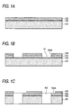
- Figs. 1A through 1D show, in sequence of procedures, the method for manufacturing an electronic component of a first exemplary embodiment. Further, the steps shown in Figs. 1E to 1G may also be performed subsequently to the steps shown in Figs. 1A through 1D.
- a first semiconductor substrate (a silicon substrate) made of, e.g., silicon, and a second semiconductor substrate (a silicon substrate) 103 made of silicon are subjected to pressurization and heating through a connection layer 102 made of, e.g., a silicon oxide film, to thus become bonded together. It is preferable to form the connection layer 102 on the first semiconductor substrate 101 or the second semiconductor substrate 103 prior to bonding together.
- connection layer 102 can be formed by means of; e.g., thermal oxidation of silicon, or the like, a technique of forming the connection layer 102 is not limited to thermal oxidation, and the connection layer may also be formed by means of various techniques such as plasma CVD, sputter, and the like.
- a mask pattern 104 having an opening 104A is formed on the second semiconductor substrate 103.
- the mask pattern 104 can be formed by patterning resist layer-which is formed by bonding, e.g., a film-like resist (a dry film resist) or by coating liquid resist-through development and exposure by means of photolithography.
- the second semiconductor substrate 103 is subjected to pattern etching (RIE: Reactive Ion Etching) using the mask pattern 104 as a mask.
- RIE Reactive Ion Etching
- a gas, plasma excitation power, pressure, and the like for etching silicon forming the second semiconductor substrate 103, a etching rate of the connection layer 102 formed from a silicon oxide film usually becomes considerably smaller in normal times. Therefore, when etching has reached the connection layer 102; namely, when a hole has penetrated through the second semiconductor substrate 103, etching is substantially suspended.
- connection layer 102 In a step shown in Fig. 1C, exposed areas of the connection layer 102 at the bottoms of the respective via holes H1 are removed by etching under conditions (a gas, plasma excitation power, pressure, and the like) complying with the composition of the connection layer 102 (e.g., a silicon oxide film). Subsequently, the conditions of etching (a gas, plasma excitation power, pressure, and the like) are made compliant with those of silicon, and then the first semiconductor substrate 101 is subjected to pattern etching (RIE). Thus, via holes H2 penetrating through the first semiconductor substrate 101, the connection layer 102, and the second semiconductor substrate 103 are formed.
- RIE pattern etching
- a mask pattern 105 having opening sections 105A is formed on the second semiconductor substrate 103.
- the mask pattern 105 can be formed by patterning a resist film which is formed by bonding, e.g., a film-like resist (a dry film resist) or by coating a liquid resist through development and exposure by means of photolithography.
- the profile (pattern) of each of the opening sections 105A corresponds to the shape of pattern wiring (trenches) formed in a subsequent step.
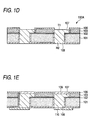
- the second semiconductor substrate 103 is subjected to pattern etching (RIE) using the mask pattern 105 as a mask. Consequently, there are formed trenches T1 which are communicated with the via holes H2 and penetrate the second semiconductor substrate 103 to thus reach the connection layer 102.
- RIE pattern etching
- connection layer 102 serves as an etch-stop layer for use in forming the trenches T1.
- via plugs 108 filling the via holes H and pattern wiring 107 filling the trenches T1 are formed integrally by plating of Cu.
- the via plugs 108 and the pattern wiring 107 are formed as follows. First, a seed layer (a feeding layer) is formed on the insulation film 106 by means of electroless plating, and a mask pattern is formed on the seed layer. Then, the via plugs 108 and the pattern wiring 107 are formed by means of electrolytic plating. Further, the mask pattern and excessive areas of the seed layer which will be uncovered by removing the mask pattern are removed. Thus, an electronic component (a wiring substrate) 100A shown in Fig. 1D can be fabricated.
- the electronic device 100A has the via plugs 108 which are made of Cu and penetrate through the first semiconductor substrate 101; and the pattern wiring 107 which is made of Cu and penetrates through the second semiconductor substrate 103, wherein at least a portion of the pattern wiring 107 substantially reaches the connection layer 102.
- connection layer 102 used for bonding two semiconductor substrates (e.g., silicon substrates) 101 and 103 is used as an etch-stop layer for forming the trenches where the pattern wiring 107 is to be formed.
- the pattern wiring 107 provided in the trenches T1 can be readily formed so as not to run over a surface of the second semiconductor substrate 103.
- pattern wiring is formed in such a way that the surface of pattern wiring 107 becomes substantially flush with the that of the second semiconductor substrate 103 or becomes recessed with respect to the surface of the second semiconductor substrate 103.
- the pattern wiring 107 has a structure of being substantially housed in the second semiconductor substrate 103, and thus it is possible to thin and downsize the electronic component 100A and enhance the reliability of pattern wiring 107.
- connection layer 102 when the first semiconductor substrate 101 and the second semiconductor substrate 103 are silicon substrates, a silicon oxide film (SiO2) or a film (SiON, SiCO, SiCON, or the like) formed by addition of nitrogen or carbon into a silicon nitride film (SiN) or a silicon oxide film may be used as the connection layer 102.
- the connection layer 102 can be used as an etch-stop layer by virtue of a difference (an etching selectivity) between an etching-amount of the substrate (silicon) and an etching-amount of the connection layer (a silicon oxide film, and the like) by means of pattern etching.
- a difference an etching selectivity
- a substrate formed by bonding two semiconductor substrates may be called a silicon-on-insulator (SOI) substrate or an SOI wafer.
- SOI silicon-on-insulator
- steps as described below may also be performed, to thus form a structure appropriate for mounting an electronic element (e.g., a semiconductor element) or to form an electronic component mounted with an electronic element.
- an electronic element e.g., a semiconductor element
- metal layers 109 and 110 made of Ni/Au are formed on the pattern wiring 107 and the via plugs 108.
- the metal layer 109 formed on the pattern wiring 107 is preferably formed so as not to run over the trenches; for instance, in such a way that the surface of the metal layer 109 becomes flush with the surface of the second semiconductor substrate 103.
- the insulation layer 111 is formed over the second semiconductor substrate 103 so as to cover the metal layer 109. Moreover, via holes penetrating through the insulation layer 111 are formed, and there are formed via plugs 112 which are buried in the via holes and are connected to the metal layer 109 and pattern wiring (electrode pads) 113 to be connected to the via plugs 112. In this case, the pattern wiring 113 is formed over the pattern wiring 107 (the metal layer 109) with the insulation layer 111 sandwiched therebetween. Namely, there are formed multilayer wirings connected to the electronic element to be mounted in the step.
- an electronic element e.g., a semiconductor element
- the pattern wiring 113 by means of bumps 115.
- the electronic component 100 it is possible to fabricate the electronic component 100 in which the electronic element (the semiconductor element) 114 is mounted on the electronic element (the wiring substrate) 100A shown in Fig. 1D.
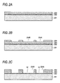
- Figs. 2A to 2I show, in sequence of procedures, the method for manufacturing an electronic component according to a second exemplary embodiment. Further, steps as shown in Figs. 2J to 2M may also be performed subsequently to the steps shown in Figs. 2A through 2I.
- a first semiconductor substrate 201 and a second semiconductor substrate 203 are subjected to pressurization and heating through a connection layer 202, to thus become bonded together, as the step shown in Fig. 1A.
- the first semiconductor substrate 201, the second semiconductor substrate 203, and the connection layer 202 of the present embodiment correspond to the first semiconductor substrate 101, the second semiconductor substrate 103, and the connection layer 102 of the first exemplary embodiment, respectively.
- a mask pattern 204 having opening sections 204A and 204B is formed on the second semiconductor substrate 203.
- the mask pattern 204 can be formed by patterning a resist layer-which is formed by bonding, e.g., a film-like resist (a dry film resist) or by coating liquid resist-through development and exposure by means of photolithography.
- the second semiconductor substrate 203 is subjected to pattern etching (RIE) using the mask pattern 204 as a mask.
- RIE pattern etching
- opening sections h1 and h2 which penetrate through the second semiconductor substrate 203, to thus reach the connection layer 202.
- the opening sections h1 correspond to via holes (via plugs) formed in a subsequent step
- the opening sections h2 correspond to recesses (cavities), which are used for mounting an electronic element, formed in a subsequent step.
- an etching rate of the connection layer 202 made of a silicon oxide film usually becomes considerably smaller. Therefore, when etching has reached the connection layer 202; namely, when a hole has penetrated through the second semiconductor substrate 203, etching is substantially suspended.
- etching may be performed using a mask pattern formed from a resist. After etching operation, a mask pattern corresponding to the mask pattern 204 (as indicated likewise by reference numeral 204 in the drawings) is again formed after removing the mask pattern.
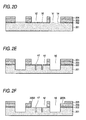
- the first semiconductor substrate 201 is etched to a predetermined depth by means of pattern etching, using the mask pattern 204 and the connection layer 202 as masks. Then, the opening sections h1 shown in Fig. 2D becomes opening sections h6 which penetrate through the second semiconductor substrate 203 and are formed in the first semiconductor substrate 201 to a predetermined depth. While the opening sections h6 are formed, there are formed opening sections h7 which are communicated with the opening sections h2 and are formed in the first semiconductor substrate 201 to a predetermined depth.
- connection layer 202 still remaining in the bottoms of the opening sections h2 are removed by etching. Further, after removing the mask pattern 204, a mask pattern 205 having openings 205A and 205B is newly formed on the second semiconductor substrate 203.
- the opening section 205A corresponds to a trench (pattern wiring) formed in a subsequent step
- the opening section 205B corresponds to a recess formed in a subsequent step.
- the first semiconductor substrate 201 and the second semiconductor substrate 203 are subjected to pattern etching (RIE) using the mask pattern 205 as a mask.
- RIE pattern etching
- Via holes BH penetrating through the first semiconductor substrate 201 and the second semiconductor substrate 203 are formed simultaneously with trenches TR which are communicated with the via holes BH and penetrate through the second semiconductor substrate 203, to thus reach the connection layer 202.
- connection layer 202 As described above, under the conditions for etching silicon, an etching rate of the connection layer 202 made of a silicon oxide film usually becomes considerably smaller. Therefore, when etching of the second semiconductor substrate 203 has reached the connection layer 202; namely, when a hole has penetrated through the second semiconductor substrate 203, etching is substantially suspended. Namely, the connection layer 202 serves as an etch-stop layer for use in forming the trenches T1.
- the opening sections h2 shown in Fig. 2F change into recesses (cavities) C which penetrate through the second semiconductor substrate 203 and are formed in the first semiconductor substrate 201 to a predetermined depth. Concurrently with formation of the recesses C, there are formed via holes bh penetrating through areas of the first semiconductor substrate 201 located in the bottoms of the respective recesses C.
- an insulation film 206 made of, for example, a silicon oxide film, is formed over the first semiconductor substrate 201 and the second semiconductor substrate 203 including interior wall surfaces of the via holes BH and bh and interior wall surfaces of the trenches TR and the recesses C.
- via plugs 208 filling the via holes BH and pattern wiring 207 filling the trenches TR are formed integrally by means of plating of; e.g., Cu.
- the via plugs 208 and the pattern wiring 207 are formed as follows. First, a seed layer (a feeding layer) is formed on the insulation film 206 by means of electroless plating, and a mask pattern is formed on the seed layer. Subsequently, the via plugs 208 and the pattern wiring 207 are formed by means of electrolytic plating. Further, the mask pattern and excessive areas of the seed layer which are uncovered as a result of removal of the mask pattern are removed.
- via plugs (via plugs for mounting an element) 209 filling the via holes bh are formed concurrently with formation of the via plugs 208 and the pattern wiring 207.
- an electronic component (a wiring substrate) 200A shown in Fig. 2I can be fabricated.
- the electronic device 200A has the via plugs 208 which are made of Cu and penetrate through the first semiconductor substrate 201; and the pattern wiring 207 which is made of Cu and penetrates through the second semiconductor substrate 203, wherein at least a portion of the pattern wiring 207 substantially reaches the connection layer 202. Further, the electronic device 200A is characterized by having the recess C which is formed in the first semiconductor substrate and the second semiconductor substrate 203 and is used for mounting an electronic element and a via plug (a via plug used for mounting an element) 209 used for connection of an electronic element.
- the method for manufacturing an electronic element is characterized in that the recess C used for mounting an electronic element (a semiconductor element) is formed. Therefore, it is possible to readily mount an electronic element and furthermore seal an electronic element into the recess C.
- steps as described below may also be performed, to thus form a structure appropriate for mounting an electronic element (e.g., a semiconductor element) or form an electronic component mounted with the electronic element.
- an electronic element e.g., a semiconductor element
- metal layers 210 and 211 made of Ni/Au are formed on the pattern wiring 207 and the via plugs 208.
- the metal layer 210 formed on the pattern wiring 207 is preferably formed so as not to run over the trenches; for instance, in such a way that the surface of the metal layer 210 becomes flush with the surface of the second semiconductor substrate 203.
- a metal layer 212 is formed on an exposed side of the via plug 209 in the recess C, and a metal layer 213 is formed on an exposed side of the via plug 209 opposite to the exposed side in the recess C.
- an electronic element e.g., a semiconductor element
- a metal layer 212 using the bumps 215.
- the electronic component shown in Fig. 2K in which the electronic element (the semiconductor element) 214 is mounted on the electronic component (the wiring substrate) 100A can be manufactured.
- the electronic element 214 may also be sealed in the recess C.
- a flat cover 216 is bonded to the second semiconductor substrate 203 by means of anodic bonding, thereby sealing the electronic element 214 in the recess C.
- the electronic element 214 when the electronic element 214 is an MEMS (Micro Electro Mechanical Systems) element, the electronic element 214 is preferably used while being sealed (enclosed) in a predetermined space. Even when the electronic element 214 is an optical-functional element, such as a light-emitting element or a light-receiving element, the electronic element 214 is preferably used while being sealed in a predetermined space as in the case of the MEMS element. According to the method for manufacturing an electronic element of the present embodiment, such an element can be sealed readily.
- MEMS Micro Electro Mechanical Systems
- the cover 216 in a case where the cover 216 is subjected to anodic bonding so as to contact the insulation film 206 made of a silicon oxide film, the cover 216 may be preferably made of silicon. Further, in a case where the electronic element is an optical-functional element (a light-emitting element or a light-receiving element), the cover 216 may be preferably made of an optically-transparent material. For example, in a case where glass is used as a material constituting the cover 216, the insulation film 206 may be preferably removed from predetermined areas before anodic bonding, and the cover (glass) 216 and the semiconductor substrate 203 (silicon) may be preferably configured to come into direct contact with each other.
- the cover (glass) 216 and the semiconductor substrate 203 silicon
- an electronic component 200 which is shown in Fig. 2M and in which the electronic element (a semiconductor element) 214 is sealed in the recess C of the electronic component (wiring substrate) 200A can be manufactured.
- the first semiconductor substrate 201 and the second semiconductor substrate 203 are sliced by means of dicing, to thus be separated into pieces.
- the number of electronic elements mounted on the wiring substrate is not limited to one, and a plurality of electronic elements may also be mounted.
- the number of recesses (cavities) formed for one electronic element is not limited to one, and a plurality of recesses may also be formed for one electronic component.
- the semiconductor substrate used in the manufacturing method is not limited to a silicon substrate, and another semiconductor substrate (e.g., SiGe) may also be used.
Landscapes
- Engineering & Computer Science (AREA)
- Microelectronics & Electronic Packaging (AREA)
- Manufacturing & Machinery (AREA)
- Internal Circuitry In Semiconductor Integrated Circuit Devices (AREA)
Abstract
Description
- This application is based on and claims priority from
Japanese Patent Application No. 2006-316201, filed on Nov. 22, 2006 - The present disclosure relates to an electronic component formed from a semiconductor substrate and a method for manufacturing the same.
- A semiconductor element such as silicon may be used for; for example, a substrate (interposer) used for mounting electronic elements such as semiconductor elements in lieu of a ceramic material or a resin material. An interposer which is made of e.g., silicon and used for mounting electronic elements exhibits superior thermal conductivity than those exhibited by the ceramic material or the resin material. For this reason, when an electronic element to be mounted generates heat, such an interposer has the advantage of exhibiting superior heat radiation.
- Further, a substrate formed from a semiconductor material is more easily precision-fabricated than the ceramic material or the resin material, and has an advantage in microfabrication. For these reasons, an interposer formed from a semiconductor material such as silicon may be adopted for an especially-microfabricated electronic component. (See e.g., Japanese Unexamined Patent Document:
JP-A-2000-39371 - However, when an electronic component is formed by use of an interposer formed from a semiconductor substrate, it is difficult to form wirings for mounting an element in such a manner that they are buried in the substrate, in light of fabrication. For instance, when wirings used for mounting an element are formed on the semiconductor substrate, the substrate gets rough. When such roughness is formed on the substrate, the reliability of connection of an electronic component may be degraded, and there also arises a problem of difficulty being encountered in thinning or downsizing the electronic component.
- In light of the above, method of manufacturing an electronic component according to independent claim 1, and an electronic component according to independent claim 8 are provided.
Further advantages, features, aspects and details are evident from the dependent claims, the description and the drawings.
Accordingly, exemplary embodiments provide a novel and useful electronic component which solves the above-described problems and a method for manufacturing the same. - Also, exemplary embodiments provide a thinned and reliable electronic component which is formed from a semiconductor substrate.
- According to the first aspect of the present invention, a method of manufacturing an electronic component comprises the steps of:
- a) forming via holes penetrating through a first semiconductor substrate and a second semiconductor substrate which are bonded together by way of a connection layer;
- b) pattern-etching the second semiconductor substrate using the connection layer as an etch-stop layer to form trenches communicated with the via holes; and
- c) integrally forming first via plugs buried in the via holes and pattern wirings buried in the trenches through plating.
- According to the second aspect of the present invention, an electronic component comprises:
- a first semiconductor substrate;
- a second semiconductor substrate bonded to the first semiconductor substrate;
- a connection layer provided between the first semiconductor substrate and the second semiconductor substrate;
- first via plugs penetrating through the first semiconductor substrate; and
- pattern wirings which penetrate through the second semiconductor substrate and are formed integrally with the via plugs, at least a portion of the patter wirings substantially reaching the connection layer.
- Embodiments are also directed to apparatuses manufactured by disclosed methods and including apparatus parts corresponding to described method steps. Furthermore, embodiments are also directed to methods by which the described apparatus is manufactured. It may include method steps for manufacturing parts of the apparatus. The method steps may be performed by way of hardware components, firmware, software, a computer programmed by appropriate software, by any combination thereof or in any other manner.
According to the present invention, it is possible to provide a thinned and highly-reliable electronic component that is formed from a semiconductor substrate. - So that the manner in which the above recited features of the present invention can be understood in detail, a more particular description of the invention, briefly summarized above, may be had by reference to embodiments. The accompanying drawings relate to embodiments of the invention and are described in the following:
- Fig. 1A is a view showing a method for manufacturing an electronic component of a first exemplary embodiment (part 1);
- Fig. 1B is a view showing the method for manufacturing an electronic component of the first exemplary embodiment (part 2);
- Fig. 1C is a view showing the method for manufacturing an electronic component of the first exemplary embodiment (part 3);
- Fig. 1D is a view showing the method for manufacturing an electronic component of the first exemplary embodiment (part 4);
- Fig. 1E is a view showing the method for manufacturing an electronic component of the first exemplary embodiment (part 5);
- Fig. 1F is a view showing the method for manufacturing an electronic component of the first exemplary embodiment (part 6);
- Fig. 1G is a view showing the method for manufacturing an electronic component of the first exemplary embodiment (part 7);
- Fig. 2A is a view showing a method for manufacturing an electronic component of a second exemplary embodiment (part 1);
- Fig. 2B is a view showing the method for manufacturing an electronic component of the second exemplary embodiment (part 2);
- Fig. 2C is a view showing the method for manufacturing an electronic component of the second exemplary embodiment (part 3);
- Fig. 2D is a view showing the method for manufacturing an electronic component of the second exemplary embodiment (part 4);
- Fig. 2E is a view showing the method for manufacturing an electronic component of the second exemplary embodiment (part 5);
- Fig. 2F is a view showing the method for manufacturing an electronic component of the second exemplary embodiment (part 6);
- Fig. 2G is a view showing the method for manufacturing an electronic component of the second exemplary embodiment (part 7);
- Fig. 2H is a view showing the method for manufacturing an electronic component of the second exemplary embodiment (part 8);
- Fig. 2I is a view showing the method for manufacturing an electronic component of the second exemplary embodiment (part 9);
- Fig. 2J is a view showing the method for manufacturing an electronic component of the second exemplary embodiment (part 10);
- Fig. 2K is a view showing the method for manufacturing an electronic component of the second exemplary embodiment (part 11);
- Fig. 2L is a view showing the method for manufacturing an electronic component of the second exemplary embodiment (part 12); and
- Fig. 2M is a view showing the method for manufacturing an electronic component of the second exemplary embodiment (part 13).
- A method of manufacturing an electronic component comprises the steps of:
- a) forming via holes penetrating through a first semiconductor substrate and a second semiconductor substrate which are bonded together by way of a connection layer;
- b) pattern-etching the second semiconductor substrate using the connection layer as an etch-stop layer to form trenches communicated with the via holes; and
- c) integrally forming first via plugs buried in the via holes and pattern wirings buried in the trenches through plating.
- Namely, the manufacturing method is characterized in that the connection layer used for bonding two semiconductor substrates (e.g., silicon substrates) is used as an etch-stop layer for use in forming the trenches in which the pattern wiring is formed.
- Therefore, it is possible to readily form the trenches for use in forming the pattern wiring. According to the above-described manufacturing method, the pattern wiring formed in the trenches can be readily formed so as not to run over a surface of the second semiconductor substrate. For instance, the pattern wiring is formed in such a way that the surface of pattern wiring becomes substantially flush with the surface of the second semiconductor substrate or becomes recessed with respect to the surface of the second semiconductor substrate.
- Namely, the pattern wiring has a structure of being substantially housed in the second semiconductor substrate, and slimming-down and miniaturization of the electronic component and enhancement of reliability of the pattern wiring become practicable.
- A specific example of the method for manufacturing an electronic device will now be described with reference to the drawings.
- Figs. 1A through 1D show, in sequence of procedures, the method for manufacturing an electronic component of a first exemplary embodiment. Further, the steps shown in Figs. 1E to 1G may also be performed subsequently to the steps shown in Figs. 1A through 1D.
- First, in a step shown in Fig. 1A, a first semiconductor substrate (a silicon substrate) made of, e.g., silicon, and a second semiconductor substrate (a silicon substrate) 103 made of silicon are subjected to pressurization and heating through a
connection layer 102 made of, e.g., a silicon oxide film, to thus become bonded together. It is preferable to form theconnection layer 102 on thefirst semiconductor substrate 101 or thesecond semiconductor substrate 103 prior to bonding together. Although theconnection layer 102 can be formed by means of; e.g., thermal oxidation of silicon, or the like, a technique of forming theconnection layer 102 is not limited to thermal oxidation, and the connection layer may also be formed by means of various techniques such as plasma CVD, sputter, and the like. - In a step shown in Fig. 1B, a
mask pattern 104 having anopening 104A is formed on thesecond semiconductor substrate 103. Themask pattern 104 can be formed by patterning resist layer-which is formed by bonding, e.g., a film-like resist (a dry film resist) or by coating liquid resist-through development and exposure by means of photolithography. - Next, the
second semiconductor substrate 103 is subjected to pattern etching (RIE: Reactive Ion Etching) using themask pattern 104 as a mask. In this case, there are formed via holes H1 which penetrate through thesecond semiconductor substrate 103 to thus reach theconnection layer 102. Under conditions (a gas, plasma excitation power, pressure, and the like) for etching silicon forming thesecond semiconductor substrate 103, a etching rate of theconnection layer 102 formed from a silicon oxide film usually becomes considerably smaller in normal times. Therefore, when etching has reached theconnection layer 102; namely, when a hole has penetrated through thesecond semiconductor substrate 103, etching is substantially suspended. - In a step shown in Fig. 1C, exposed areas of the
connection layer 102 at the bottoms of the respective via holes H1 are removed by etching under conditions (a gas, plasma excitation power, pressure, and the like) complying with the composition of the connection layer 102 (e.g., a silicon oxide film). Subsequently, the conditions of etching (a gas, plasma excitation power, pressure, and the like) are made compliant with those of silicon, and then thefirst semiconductor substrate 101 is subjected to pattern etching (RIE). Thus, via holes H2 penetrating through thefirst semiconductor substrate 101, theconnection layer 102, and thesecond semiconductor substrate 103 are formed. - Next, after removing the
mask pattern 104, amask pattern 105 havingopening sections 105A is formed on thesecond semiconductor substrate 103. Themask pattern 105 can be formed by patterning a resist film which is formed by bonding, e.g., a film-like resist (a dry film resist) or by coating a liquid resist through development and exposure by means of photolithography. The profile (pattern) of each of the openingsections 105A corresponds to the shape of pattern wiring (trenches) formed in a subsequent step. - Next, in a step shown in Fig. 1D, the
second semiconductor substrate 103 is subjected to pattern etching (RIE) using themask pattern 105 as a mask. Consequently, there are formed trenches T1 which are communicated with the via holes H2 and penetrate thesecond semiconductor substrate 103 to thus reach theconnection layer 102. - As described above, under the conditions for etching silicon constituting the
second semiconductor substrate 103, an etching rate of theconnection layer 102 formed from a silicon oxide film usually becomes considerably smaller in normal times. Therefore, when etching of thesecond semiconductor substrate 103 has reached theconnection layer 102; namely, when a hole has penetrated through thesecond semiconductor substrate 103, etching is substantially suspended. In other words, theconnection layer 102 serves as an etch-stop layer for use in forming the trenches T1. - Next, an
insulation film 106 made of; e.g., a silicon oxide film, is formed over the surface of thefirst semiconductor substrate 101 and thesecond semiconductor substrate 103 including interior wall surfaces of the via holes H2 and interior wall surfaces of the trenches T1. - Next, via
plugs 108 filling the via holes H andpattern wiring 107 filling the trenches T1 are formed integrally by plating of Cu. The via plugs 108 and thepattern wiring 107 are formed as follows. First, a seed layer (a feeding layer) is formed on theinsulation film 106 by means of electroless plating, and a mask pattern is formed on the seed layer. Then, the via plugs 108 and thepattern wiring 107 are formed by means of electrolytic plating. Further, the mask pattern and excessive areas of the seed layer which will be uncovered by removing the mask pattern are removed. Thus, an electronic component (a wiring substrate) 100A shown in Fig. 1D can be fabricated. - The
electronic device 100A has the via plugs 108 which are made of Cu and penetrate through thefirst semiconductor substrate 101; and thepattern wiring 107 which is made of Cu and penetrates through thesecond semiconductor substrate 103, wherein at least a portion of thepattern wiring 107 substantially reaches theconnection layer 102. - The above-described method of manufacturing a semiconductor device is
characterized in that theconnection layer 102 used for bonding two semiconductor substrates (e.g., silicon substrates) 101 and 103 is used as an etch-stop layer for forming the trenches where thepattern wiring 107 is to be formed. - Therefore, it is possible to readily form the trenches T1 used for forming the
pattern wiring 107. Further, according to the manufacturing method, thepattern wiring 107 provided in the trenches T1 can be readily formed so as not to run over a surface of thesecond semiconductor substrate 103. For instance, pattern wiring is formed in such a way that the surface ofpattern wiring 107 becomes substantially flush with the that of thesecond semiconductor substrate 103 or becomes recessed with respect to the surface of thesecond semiconductor substrate 103. - Namely, the
pattern wiring 107 has a structure of being substantially housed in thesecond semiconductor substrate 103, and thus it is possible to thin and downsize theelectronic component 100A and enhance the reliability ofpattern wiring 107. - For instance, when the
first semiconductor substrate 101 and thesecond semiconductor substrate 103 are silicon substrates, a silicon oxide film (SiO2) or a film (SiON, SiCO, SiCON, or the like) formed by addition of nitrogen or carbon into a silicon nitride film (SiN) or a silicon oxide film may be used as theconnection layer 102. In this case, theconnection layer 102 can be used as an etch-stop layer by virtue of a difference (an etching selectivity) between an etching-amount of the substrate (silicon) and an etching-amount of the connection layer (a silicon oxide film, and the like) by means of pattern etching. Thus, it is possible to readily form the trenches T1 and thepattern wiring 107. - As mentioned above, a substrate formed by bonding two semiconductor substrates (wafers) may be called a silicon-on-insulator (SOI) substrate or an SOI wafer.
- Subsequently to the step shown in Fig. 1D, steps as described below may also be performed, to thus form a structure appropriate for mounting an electronic element (e.g., a semiconductor element) or to form an electronic component mounted with an electronic element.
- For instance, in a step shown in Fig. 1E,
metal layers pattern wiring 107 and the via plugs 108. In this case, themetal layer 109 formed on thepattern wiring 107 is preferably formed so as not to run over the trenches; for instance, in such a way that the surface of themetal layer 109 becomes flush with the surface of thesecond semiconductor substrate 103. - In a step shown in Fig. 1F, the
insulation layer 111 is formed over thesecond semiconductor substrate 103 so as to cover themetal layer 109. Moreover, via holes penetrating through theinsulation layer 111 are formed, and there are formed viaplugs 112 which are buried in the via holes and are connected to themetal layer 109 and pattern wiring (electrode pads) 113 to be connected to the via plugs 112. In this case, thepattern wiring 113 is formed over the pattern wiring 107 (the metal layer 109) with theinsulation layer 111 sandwiched therebetween. Namely, there are formed multilayer wirings connected to the electronic element to be mounted in the step. - In a step shown in Fig. 1G, an electronic element (e.g., a semiconductor element) 114 is connected to the
pattern wiring 113 by means ofbumps 115. Thus, it is possible to fabricate theelectronic component 100 in which the electronic element (the semiconductor element) 114 is mounted on the electronic element (the wiring substrate) 100A shown in Fig. 1D. - In the method of manufacturing an electronic component, an example of portions of specific areas of the
first semiconductor substrate 101 and thesecond semiconductor substrate 103 is described. In usual, a plurality of areas as shown in Figs. 1A to 1C are formed in a grid pattern in thefirst semiconductor substrate 101 and thesecond semiconductor substrate 103. In any of the steps shown in Figs. 1D to 1 G, thefirst semiconductor substrate 101 and thesecond semiconductor substrate 103 are sliced by means of dicing, to thus be separated into pieces. - Figs. 2A to 2I show, in sequence of procedures, the method for manufacturing an electronic component according to a second exemplary embodiment. Further, steps as shown in Figs. 2J to 2M may also be performed subsequently to the steps shown in Figs. 2A through 2I.
- First, in a step shown in Fig. 2A, a
first semiconductor substrate 201 and asecond semiconductor substrate 203 are subjected to pressurization and heating through aconnection layer 202, to thus become bonded together, as the step shown in Fig. 1A. Thefirst semiconductor substrate 201, thesecond semiconductor substrate 203, and theconnection layer 202 of the present embodiment correspond to thefirst semiconductor substrate 101, thesecond semiconductor substrate 103, and theconnection layer 102 of the first exemplary embodiment, respectively. - In a step shown in Fig. 2B, a
mask pattern 204 havingopening sections second semiconductor substrate 203. Themask pattern 204 can be formed by patterning a resist layer-which is formed by bonding, e.g., a film-like resist (a dry film resist) or by coating liquid resist-through development and exposure by means of photolithography. - Next, the
second semiconductor substrate 203 is subjected to pattern etching (RIE) using themask pattern 204 as a mask. In this case, there are formed opening sections h1 and h2 which penetrate through thesecond semiconductor substrate 203, to thus reach theconnection layer 202. The opening sections h1 correspond to via holes (via plugs) formed in a subsequent step, and the opening sections h2 correspond to recesses (cavities), which are used for mounting an electronic element, formed in a subsequent step. - Under conditions for etching silicon constituting the
second semiconductor substrate 203, an etching rate of theconnection layer 202 made of a silicon oxide film usually becomes considerably smaller. Therefore, when etching has reached theconnection layer 202; namely, when a hole has penetrated through thesecond semiconductor substrate 203, etching is substantially suspended. - In a step shown in Fig. 2D, exposed areas of the
connection layer 202 at the bottoms of the respective opening sections h1 are removed by etching. Consequently, opening sections h4 are formed in theconnection layer 202, and then thefirst semiconductor substrate 201 is exposed. Likewise, some of the exposed areas of theconnection layer 202 at the bottom of the respective opening sections h2 are removed in the form of a plurality of circles by means of pattern etching, to thus form opening sections h5. As a result, thefirst semiconductor substrate 201 becomes exposed through the opening sections h5. Thefirst semiconductor substrate 201 becomes exposed through the opening sections h5. According to pattern-etching of theconnection layer 202 in the present step, etching may be performed using a mask pattern formed from a resist. After etching operation, a mask pattern corresponding to the mask pattern 204 (as indicated likewise byreference numeral 204 in the drawings) is again formed after removing the mask pattern. - In a step shown in Fig. 2E, the
first semiconductor substrate 201 is etched to a predetermined depth by means of pattern etching, using themask pattern 204 and theconnection layer 202 as masks. Then, the opening sections h1 shown in Fig. 2D becomes opening sections h6 which penetrate through thesecond semiconductor substrate 203 and are formed in thefirst semiconductor substrate 201 to a predetermined depth. While the opening sections h6 are formed, there are formed opening sections h7 which are communicated with the opening sections h2 and are formed in thefirst semiconductor substrate 201 to a predetermined depth. - In a step shown in Fig. 2F, the
connection layer 202 still remaining in the bottoms of the opening sections h2 are removed by etching. Further, after removing themask pattern 204, amask pattern 205 havingopenings second semiconductor substrate 203. In this case, theopening section 205A corresponds to a trench (pattern wiring) formed in a subsequent step, and theopening section 205B corresponds to a recess formed in a subsequent step. - In a step shown in Fig. 2G, the
first semiconductor substrate 201 and thesecond semiconductor substrate 203 are subjected to pattern etching (RIE) using themask pattern 205 as a mask. Via holes BH penetrating through thefirst semiconductor substrate 201 and thesecond semiconductor substrate 203 are formed simultaneously with trenches TR which are communicated with the via holes BH and penetrate through thesecond semiconductor substrate 203, to thus reach theconnection layer 202. - As described above, under the conditions for etching silicon, an etching rate of the
connection layer 202 made of a silicon oxide film usually becomes considerably smaller. Therefore, when etching of thesecond semiconductor substrate 203 has reached theconnection layer 202; namely, when a hole has penetrated through thesecond semiconductor substrate 203, etching is substantially suspended. Namely, theconnection layer 202 serves as an etch-stop layer for use in forming the trenches T1. - In the present step, the opening sections h2 shown in Fig. 2F change into recesses (cavities) C which penetrate through the
second semiconductor substrate 203 and are formed in thefirst semiconductor substrate 201 to a predetermined depth. Concurrently with formation of the recesses C, there are formed via holes bh penetrating through areas of thefirst semiconductor substrate 201 located in the bottoms of the respective recesses C. - In a step shown in Fig. 2H, an
insulation film 206 made of, for example, a silicon oxide film, is formed over thefirst semiconductor substrate 201 and thesecond semiconductor substrate 203 including interior wall surfaces of the via holes BH and bh and interior wall surfaces of the trenches TR and the recesses C. - Next, in a step shown in Fig. 2I, via
plugs 208 filling the via holes BH andpattern wiring 207 filling the trenches TR are formed integrally by means of plating of; e.g., Cu. The via plugs 208 and thepattern wiring 207 are formed as follows. First, a seed layer (a feeding layer) is formed on theinsulation film 206 by means of electroless plating, and a mask pattern is formed on the seed layer. Subsequently, the via plugs 208 and thepattern wiring 207 are formed by means of electrolytic plating. Further, the mask pattern and excessive areas of the seed layer which are uncovered as a result of removal of the mask pattern are removed. Moreover, via plugs (via plugs for mounting an element) 209 filling the via holes bh are formed concurrently with formation of the via plugs 208 and thepattern wiring 207. Thus, an electronic component (a wiring substrate) 200A shown in Fig. 2I can be fabricated. - The
electronic device 200A has the via plugs 208 which are made of Cu and penetrate through thefirst semiconductor substrate 201; and thepattern wiring 207 which is made of Cu and penetrates through thesecond semiconductor substrate 203, wherein at least a portion of thepattern wiring 207 substantially reaches theconnection layer 202. Further, theelectronic device 200A is characterized by having the recess C which is formed in the first semiconductor substrate and thesecond semiconductor substrate 203 and is used for mounting an electronic element and a via plug (a via plug used for mounting an element) 209 used for connection of an electronic element. - In addition to yielding the same advantage as that yielded in the first exemplary embodiment, the method for manufacturing an electronic element is characterized in that the recess C used for mounting an electronic element (a semiconductor element) is formed. Therefore, it is possible to readily mount an electronic element and furthermore seal an electronic element into the recess C.
- In a step subsequent to the step shown in Fig. 2I, steps as described below may also be performed, to thus form a structure appropriate for mounting an electronic element (e.g., a semiconductor element) or form an electronic component mounted with the electronic element.
- For instance, in a step shown in Fig. 2J,
metal layers pattern wiring 207 and the via plugs 208. In this case, themetal layer 210 formed on thepattern wiring 207 is preferably formed so as not to run over the trenches; for instance, in such a way that the surface of themetal layer 210 becomes flush with the surface of thesecond semiconductor substrate 203. - In the same manner as mentioned above, a
metal layer 212 is formed on an exposed side of the viaplug 209 in the recess C, and ametal layer 213 is formed on an exposed side of the viaplug 209 opposite to the exposed side in the recess C. - In a step shown in Fig. 2K, an electronic element (e.g., a semiconductor element) 214 is connected to the via plugs 209 through a
metal layer 212 using thebumps 215. Thus, the electronic component shown in Fig. 2K in which the electronic element (the semiconductor element) 214 is mounted on the electronic component (the wiring substrate) 100A can be manufactured. - In a step shown in Fig. 2L, the
electronic element 214 may also be sealed in the recess C. For instance, in a step shown in Fig. 2L, aflat cover 216 is bonded to thesecond semiconductor substrate 203 by means of anodic bonding, thereby sealing theelectronic element 214 in the recess C. - For instance, when the
electronic element 214 is an MEMS (Micro Electro Mechanical Systems) element, theelectronic element 214 is preferably used while being sealed (enclosed) in a predetermined space. Even when theelectronic element 214 is an optical-functional element, such as a light-emitting element or a light-receiving element, theelectronic element 214 is preferably used while being sealed in a predetermined space as in the case of the MEMS element. According to the method for manufacturing an electronic element of the present embodiment, such an element can be sealed readily. - For example, in a case where the
cover 216 is subjected to anodic bonding so as to contact theinsulation film 206 made of a silicon oxide film, thecover 216 may be preferably made of silicon. Further, in a case where the electronic element is an optical-functional element (a light-emitting element or a light-receiving element), thecover 216 may be preferably made of an optically-transparent material. For example, in a case where glass is used as a material constituting thecover 216, theinsulation film 206 may be preferably removed from predetermined areas before anodic bonding, and the cover (glass) 216 and the semiconductor substrate 203 (silicon) may be preferably configured to come into direct contact with each other. - Through the above steps, an
electronic component 200 which is shown in Fig. 2M and in which the electronic element (a semiconductor element) 214 is sealed in the recess C of the electronic component (wiring substrate) 200A can be manufactured. - In the method for manufacturing the electronic component, an example of portions of specific areas of the
first semiconductor substrate 201 and thesecond semiconductor substrate 203 is described. In usual, a plurality of areas as shown in Figs. 2A to 2H are formed in a grid pattern in thefirst semiconductor substrate 201 and thesecond semiconductor substrate 203. In any of the steps shown in Figs. 2I to 2M, thefirst semiconductor substrate 201 and thesecond semiconductor substrate 203 are sliced by means of dicing, to thus be separated into pieces. - According to the exemplary embodiments, the number of electronic elements mounted on the wiring substrate is not limited to one, and a plurality of electronic elements may also be mounted. Also, the number of recesses (cavities) formed for one electronic element is not limited to one, and a plurality of recesses may also be formed for one electronic component.
- According to the exemplary embodiments, the semiconductor substrate used in the manufacturing method (for an electronic component) is not limited to a silicon substrate, and another semiconductor substrate (e.g., SiGe) may also be used.
- According to the exemplary embodiments, it is possible to provide a thinned and highly-reliable electronic component which is formed from a semiconductor substrate.
- While there has been described in connection with the exemplary embodiments of the present invention, it will be obvious to those skilled in the art that various changes and modification may be made therein without departing from the present invention. It is aimed, therefore, to cover in the appended claim all such changes and modifications as fall within the true spirit and scope of the present invention.
Claims (12)
- A method of manufacturing an electronic component (100, 100A; 200) comprising the steps of:a) forming via holes (H2; BH) penetrating through a first semiconductor substrate (101; 201) and a second semiconductor substrate (103; 203) which are bonded together by way of a connection layer (102; 202);b) pattern-etching the second semiconductor substrate using the connection layer as an etch-stop layer to form trenches (T1; TR) communicated with the via holes; andc) integrally forming first via plugs (108; 208, 209) buried in the via holes and pattern wirings (107; 207) buried in the trenches through plating.
- The method of manufacturing an electronic component according to claim 1, further comprising the step of:d) mounting an electronic element (114; 214) connected to the pattern wirings.
- The method of manufacturing an electronic component according to any of claims 1 to 2, further comprising the steps of:e) pattern-etching the first semiconductor substrate and the second semiconductor substrate to form a recess (C) where an electronic element is mounted; andf) forming second via plugs (209) which penetrate through bottoms of the recesses and are connected to the electronic element mounted on the recesses.
- The method of manufacturing an electronic component according to claim 3, further comprising the step of:g) mounting an electronic element (214) connected to the second via plugs.
- The method of manufacturing an electronic component according to claim 4, further comprising the step of:h) sealing the electronic element in the recess by means of a flat cover (216).
- The method of manufacturing an electronic component according to any of claims 1 to 5, wherein an etching rate of the connection layer is much smaller than that of the second semiconductor substrate.
- The method of manufacturing an electronic component according to any of claims 1 to 6, wherein the connection layer (102; 202) is made of SiO2 and the second semiconductor substrate (103; 203) is made of Si.
- An electronic component (100, 100A; 200) comprising:a first semiconductor substrate (101; 201);a second semiconductor substrate (103; 203) bonded to the first semiconductor substrate;a connection layer (102; 202) provided between the first semiconductor substrate and the second semiconductor substrate;first via plugs (108; 208, 209) penetrating through the first semiconductor substrate; andpattern wirings (107; 207) which penetrate through the second semiconductor substrate and are formed integrally with the via plugs, at least a portion of the patter wirings substantially reaching the connection layer.
- The electronic component according to claim 8, further comprising:an electronic element (114; 214) connected to the pattern wiring.
- The electronic component according to claims 8 to 9, further comprising:a recess (C) which is formed in the first semiconductor substrate and the second semiconductor substrate and in which the electronic element is mounted; andsecond via plugs (209) which penetrate through bottom of the recess and is connected to the electronic element.
- The electronic component according to claim 10, further comprising:an electronic element (214) connected to the second via plugs.
- The electronic component according to claim 11, further comprising:a flat cover (216) which seals the electronic element in the recess.
Applications Claiming Priority (1)
| Application Number | Priority Date | Filing Date | Title |
|---|---|---|---|
| JP2006316201A JP5179046B2 (en) | 2006-11-22 | 2006-11-22 | Electronic component and method for manufacturing electronic component |
Publications (3)
| Publication Number | Publication Date |
|---|---|
| EP1926135A2 true EP1926135A2 (en) | 2008-05-28 |
| EP1926135A3 EP1926135A3 (en) | 2008-10-29 |
| EP1926135B1 EP1926135B1 (en) | 2017-01-11 |
Family
ID=39185771
Family Applications (1)
| Application Number | Title | Priority Date | Filing Date |
|---|---|---|---|
| EP07022678.2A Ceased EP1926135B1 (en) | 2006-11-22 | 2007-11-22 | Electronic component and method for manufacturing the same |
Country Status (5)
| Country | Link |
|---|---|
| US (1) | US7948092B2 (en) |
| EP (1) | EP1926135B1 (en) |
| JP (1) | JP5179046B2 (en) |
| KR (1) | KR101406897B1 (en) |
| TW (1) | TWI442545B (en) |
Cited By (1)
| Publication number | Priority date | Publication date | Assignee | Title |
|---|---|---|---|---|
| EP2826066A4 (en) * | 2012-03-12 | 2015-12-16 | Silex Microsystems Ab | SEMICONDUCTOR DEVICES WITH TIGHT STRUCTURES OF IN-LINE ROUTING INTERCONNECTION HOLES AND METHOD FOR MANUFACTURING THE SAME |
Families Citing this family (10)
| Publication number | Priority date | Publication date | Assignee | Title |
|---|---|---|---|---|
| KR101002680B1 (en) * | 2008-10-21 | 2010-12-21 | 삼성전기주식회사 | Semiconductor package and manufacturing method thereof |
| JP5330115B2 (en) * | 2009-06-17 | 2013-10-30 | 浜松ホトニクス株式会社 | Multilayer wiring board |
| US9337116B2 (en) * | 2010-10-28 | 2016-05-10 | Stats Chippac, Ltd. | Semiconductor device and method of forming stepped interposer for stacking and electrically connecting semiconductor die |
| US9129943B1 (en) * | 2012-03-29 | 2015-09-08 | Amkor Technology, Inc. | Embedded component package and fabrication method |
| US9123780B2 (en) * | 2012-12-19 | 2015-09-01 | Invensas Corporation | Method and structures for heat dissipating interposers |
| JP6274058B2 (en) * | 2014-09-22 | 2018-02-07 | 株式会社デンソー | Electronic device and electronic structure including electronic device |
| US9768145B2 (en) * | 2015-08-31 | 2017-09-19 | Taiwan Semiconductor Manufacturing Company, Ltd. | Methods of forming multi-die package structures including redistribution layers |
| US11355427B2 (en) * | 2016-07-01 | 2022-06-07 | Intel Corporation | Device, method and system for providing recessed interconnect structures of a substrate |
| WO2018216693A1 (en) * | 2017-05-23 | 2018-11-29 | 京セラ株式会社 | Multi-piece wiring substrate, electronic component housing package, and electronic device |
| CN119626993A (en) * | 2024-02-26 | 2025-03-14 | 芯爱科技(南京)有限公司 | Electronic packaging and method of manufacturing the same |
Citations (2)
| Publication number | Priority date | Publication date | Assignee | Title |
|---|---|---|---|---|
| JP2000039371A (en) | 1998-07-21 | 2000-02-08 | Denso Corp | Semiconductor pressure sensor and method of manufacturing the same |
| EP1261021A2 (en) | 2001-05-21 | 2002-11-27 | Shinko Electric Industries Co. Ltd. | Method of production of circuit board, semiconductor device, and plating system |
Family Cites Families (14)
| Publication number | Priority date | Publication date | Assignee | Title |
|---|---|---|---|---|
| JP2617798B2 (en) * | 1989-09-22 | 1997-06-04 | 三菱電機株式会社 | Stacked semiconductor device and method of manufacturing the same |
| JPH05198739A (en) * | 1991-09-10 | 1993-08-06 | Mitsubishi Electric Corp | Stacked semiconductor device and manufacturing method thereof |
| US5455445A (en) * | 1994-01-21 | 1995-10-03 | Kulite Semiconductor Products, Inc. | Multi-level semiconductor structures having environmentally isolated elements |
| US6444576B1 (en) * | 2000-06-16 | 2002-09-03 | Chartered Semiconductor Manufacturing, Ltd. | Three dimensional IC package module |
| US6352921B1 (en) * | 2000-07-19 | 2002-03-05 | Chartered Semiconductor Manufacturing Ltd. | Use of boron carbide as an etch-stop and barrier layer for copper dual damascene metallization |
| US6355501B1 (en) * | 2000-09-21 | 2002-03-12 | International Business Machines Corporation | Three-dimensional chip stacking assembly |
| JP2003258189A (en) * | 2002-03-01 | 2003-09-12 | Toshiba Corp | Semiconductor device and manufacturing method thereof |
| US6642081B1 (en) * | 2002-04-11 | 2003-11-04 | Robert Patti | Interlocking conductor method for bonding wafers to produce stacked integrated circuits |
| KR100596423B1 (en) * | 2004-12-28 | 2006-07-06 | 주식회사 하이닉스반도체 | Semiconductor memory device and manufacturing method thereof |
| KR100596420B1 (en) * | 2004-12-28 | 2006-07-06 | 주식회사 하이닉스반도체 | Manufacturing method of semiconductor memory device having recessed storage node contact plug |
| FR2883612B1 (en) | 2005-03-22 | 2010-09-10 | Peugeot Citroen Automobiles Sa | DOUBLE-COVER CROSS-FLOW DAMPING DEVICE WITHOUT INDEXING |
| US7262622B2 (en) * | 2005-03-24 | 2007-08-28 | Memsic, Inc. | Wafer-level package for integrated circuits |
| JP4979213B2 (en) * | 2005-08-31 | 2012-07-18 | オンセミコンダクター・トレーディング・リミテッド | Circuit board, circuit board manufacturing method, and circuit device |
| EP2067167B1 (en) | 2006-09-22 | 2016-04-13 | Ipdia | Method for making an electronic device |
-
2006
- 2006-11-22 JP JP2006316201A patent/JP5179046B2/en not_active Expired - Fee Related
-
2007
- 2007-11-20 US US11/943,203 patent/US7948092B2/en not_active Expired - Fee Related
- 2007-11-21 KR KR1020070119046A patent/KR101406897B1/en not_active Expired - Fee Related
- 2007-11-22 EP EP07022678.2A patent/EP1926135B1/en not_active Ceased
- 2007-11-22 TW TW096144265A patent/TWI442545B/en not_active IP Right Cessation
Patent Citations (2)
| Publication number | Priority date | Publication date | Assignee | Title |
|---|---|---|---|---|
| JP2000039371A (en) | 1998-07-21 | 2000-02-08 | Denso Corp | Semiconductor pressure sensor and method of manufacturing the same |
| EP1261021A2 (en) | 2001-05-21 | 2002-11-27 | Shinko Electric Industries Co. Ltd. | Method of production of circuit board, semiconductor device, and plating system |
Cited By (3)
| Publication number | Priority date | Publication date | Assignee | Title |
|---|---|---|---|---|
| EP2826066A4 (en) * | 2012-03-12 | 2015-12-16 | Silex Microsystems Ab | SEMICONDUCTOR DEVICES WITH TIGHT STRUCTURES OF IN-LINE ROUTING INTERCONNECTION HOLES AND METHOD FOR MANUFACTURING THE SAME |
| US9240373B2 (en) | 2012-03-12 | 2016-01-19 | Silex Microsystems Ab | Semiconductor devices with close-packed via structures having in-plane routing and method of making same |
| US9484293B2 (en) | 2012-03-12 | 2016-11-01 | Silex Microsystems Ab | Semiconductor devices with close-packed via structures having in-plane routing and method of making same |
Also Published As
| Publication number | Publication date |
|---|---|
| KR101406897B1 (en) | 2014-06-13 |
| US20080116566A1 (en) | 2008-05-22 |
| JP5179046B2 (en) | 2013-04-10 |
| JP2008130933A (en) | 2008-06-05 |
| EP1926135B1 (en) | 2017-01-11 |
| EP1926135A3 (en) | 2008-10-29 |
| KR20080046587A (en) | 2008-05-27 |
| TW200832675A (en) | 2008-08-01 |
| TWI442545B (en) | 2014-06-21 |
| US7948092B2 (en) | 2011-05-24 |
Similar Documents
| Publication | Publication Date | Title |
|---|---|---|
| EP1926135B1 (en) | Electronic component and method for manufacturing the same | |
| US12391545B2 (en) | Semiconductor device and method for fabricating the same | |
| JP4919984B2 (en) | Electronic device package and method for forming the same | |
| CN102134054B (en) | Method for fabricating a microelectromechanical system device | |
| TWI636001B (en) | Hybrid integrated component and method of manufacturing same | |
| JP5133867B2 (en) | Package for micro components | |
| US7705451B2 (en) | Semiconductor device and method of manufacturing the same | |
| CN101517729A (en) | Formation of through-wafer electrical interconnections and other structures using a thin dielectric membrane | |
| CN103295985A (en) | Chip package and method for forming the same | |
| CN101312161A (en) | Electronic structures and fabrication methods thereof | |
| US7618837B2 (en) | Method for fabricating high aspect ratio MEMS device with integrated circuit on the same substrate using post-CMOS process | |
| JP2005129888A (en) | Sensor device and sensor system, and manufacturing method therefor | |
| JP2008066481A (en) | Package, semiconductor device, package manufacturing method, and semiconductor device manufacturing method | |
| JP4069028B2 (en) | Substrate with through electrode, method for manufacturing the same, and electronic device | |
| US20200059721A1 (en) | Method for manufacturing air pulse generating element | |
| JP4285604B2 (en) | Substrate with through electrode, method for manufacturing the same, and electronic device | |
| KR100872404B1 (en) | Wafer Bonding Packaging Method | |
| CN102891120A (en) | Chip package and method of forming the same | |
| CN117623216A (en) | MEMS device, preparation method thereof and electronic device | |
| CN102891133A (en) | Chip package and method of forming the same | |
| KR101468641B1 (en) | Semiconductor device and fabrication method thereof | |
| CN120403625A (en) | Method for forming inertial sensor, inertial sensor, and electronic device | |
| HK1121731B (en) | Thin package for a micro component |
Legal Events
| Date | Code | Title | Description |
|---|---|---|---|
| PUAI | Public reference made under article 153(3) epc to a published international application that has entered the european phase |
Free format text: ORIGINAL CODE: 0009012 |
|
| AK | Designated contracting states |
Kind code of ref document: A2 Designated state(s): AT BE BG CH CY CZ DE DK EE ES FI FR GB GR HU IE IS IT LI LT LU LV MC MT NL PL PT RO SE SI SK TR |
|
| AX | Request for extension of the european patent |
Extension state: AL BA HR MK RS |
|
| PUAL | Search report despatched |
Free format text: ORIGINAL CODE: 0009013 |
|
| AK | Designated contracting states |
Kind code of ref document: A3 Designated state(s): AT BE BG CH CY CZ DE DK EE ES FI FR GB GR HU IE IS IT LI LT LU LV MC MT NL PL PT RO SE SI SK TR |
|
| AX | Request for extension of the european patent |
Extension state: AL BA HR MK RS |
|
| 17P | Request for examination filed |
Effective date: 20090428 |
|
| AKX | Designation fees paid |
Designated state(s): DE |
|
| 17Q | First examination report despatched |
Effective date: 20150824 |
|
| REG | Reference to a national code |
Ref country code: DE Ref legal event code: R079 Ref document number: 602007049473 Country of ref document: DE Free format text: PREVIOUS MAIN CLASS: H01L0021480000 Ipc: H01L0023020000 |
|
| GRAP | Despatch of communication of intention to grant a patent |
Free format text: ORIGINAL CODE: EPIDOSNIGR1 |
|
| RIC1 | Information provided on ipc code assigned before grant |
Ipc: H01L 23/498 20060101ALI20160531BHEP Ipc: H01L 23/13 20060101ALI20160531BHEP Ipc: B81C 1/00 20060101ALI20160531BHEP Ipc: H01L 23/02 20060101AFI20160531BHEP Ipc: H01L 23/14 20060101ALI20160531BHEP Ipc: H01L 21/48 20060101ALI20160531BHEP Ipc: H01L 21/768 20060101ALI20160531BHEP |
|
| INTG | Intention to grant announced |
Effective date: 20160617 |
|
| GRAJ | Information related to disapproval of communication of intention to grant by the applicant or resumption of examination proceedings by the epo deleted |
Free format text: ORIGINAL CODE: EPIDOSDIGR1 |
|
| GRAR | Information related to intention to grant a patent recorded |
Free format text: ORIGINAL CODE: EPIDOSNIGR71 |
|
| GRAS | Grant fee paid |
Free format text: ORIGINAL CODE: EPIDOSNIGR3 |
|
| INTC | Intention to grant announced (deleted) | ||
| GRAA | (expected) grant |
Free format text: ORIGINAL CODE: 0009210 |
|
| INTG | Intention to grant announced |
Effective date: 20161115 |
|
| AK | Designated contracting states |
Kind code of ref document: B1 Designated state(s): DE |
|
| REG | Reference to a national code |
Ref country code: DE Ref legal event code: R096 Ref document number: 602007049473 Country of ref document: DE |
|
| REG | Reference to a national code |
Ref country code: DE Ref legal event code: R097 Ref document number: 602007049473 Country of ref document: DE |
|
| PLBE | No opposition filed within time limit |
Free format text: ORIGINAL CODE: 0009261 |
|
| STAA | Information on the status of an ep patent application or granted ep patent |
Free format text: STATUS: NO OPPOSITION FILED WITHIN TIME LIMIT |
|
| 26N | No opposition filed |
Effective date: 20171012 |
|
| PGFP | Annual fee paid to national office [announced via postgrant information from national office to epo] |
Ref country code: DE Payment date: 20181106 Year of fee payment: 12 |
|
| REG | Reference to a national code |
Ref country code: DE Ref legal event code: R119 Ref document number: 602007049473 Country of ref document: DE |
|
| PG25 | Lapsed in a contracting state [announced via postgrant information from national office to epo] |
Ref country code: DE Free format text: LAPSE BECAUSE OF NON-PAYMENT OF DUE FEES Effective date: 20200603 |