EP1921908A2 - Circuit assembly with a power module that is combined with a circuit board - Google Patents
Circuit assembly with a power module that is combined with a circuit board Download PDFInfo
- Publication number
- EP1921908A2 EP1921908A2 EP07021363A EP07021363A EP1921908A2 EP 1921908 A2 EP1921908 A2 EP 1921908A2 EP 07021363 A EP07021363 A EP 07021363A EP 07021363 A EP07021363 A EP 07021363A EP 1921908 A2 EP1921908 A2 EP 1921908A2
- Authority
- EP
- European Patent Office
- Prior art keywords
- housing
- circuit board
- circuit arrangement
- cup
- power module
- Prior art date
- Legal status (The legal status is an assumption and is not a legal conclusion. Google has not performed a legal analysis and makes no representation as to the accuracy of the status listed.)
- Granted
Links
Images

Classifications
-
- H—ELECTRICITY
- H05—ELECTRIC TECHNIQUES NOT OTHERWISE PROVIDED FOR
- H05K—PRINTED CIRCUITS; CASINGS OR CONSTRUCTIONAL DETAILS OF ELECTRIC APPARATUS; MANUFACTURE OF ASSEMBLAGES OF ELECTRICAL COMPONENTS
- H05K3/00—Apparatus or processes for manufacturing printed circuits
- H05K3/30—Assembling printed circuits with electric components, e.g. with resistors
- H05K3/32—Assembling printed circuits with electric components, e.g. with resistors electrically connecting electric components or wires to printed circuits
- H05K3/325—Assembling printed circuits with electric components, e.g. with resistors electrically connecting electric components or wires to printed circuits by abutting or pinching; Mechanical auxiliary parts therefor
-
- H—ELECTRICITY
- H05—ELECTRIC TECHNIQUES NOT OTHERWISE PROVIDED FOR
- H05K—PRINTED CIRCUITS; CASINGS OR CONSTRUCTIONAL DETAILS OF ELECTRIC APPARATUS; MANUFACTURE OF ASSEMBLAGES OF ELECTRICAL COMPONENTS
- H05K1/00—Printed circuits
- H05K1/02—Details
- H05K1/14—Structural association of two or more printed circuits
- H05K1/141—One or more single auxiliary printed circuits mounted on a main printed circuit, e.g. modules, adapters
-
- H—ELECTRICITY
- H05—ELECTRIC TECHNIQUES NOT OTHERWISE PROVIDED FOR
- H05K—PRINTED CIRCUITS; CASINGS OR CONSTRUCTIONAL DETAILS OF ELECTRIC APPARATUS; MANUFACTURE OF ASSEMBLAGES OF ELECTRICAL COMPONENTS
- H05K2201/00—Indexing scheme relating to printed circuits covered by H05K1/00
- H05K2201/10—Details of components or other objects attached to or integrated in a printed circuit board
- H05K2201/10431—Details of mounted components
- H05K2201/10575—Insulating foil under component
-
- H—ELECTRICITY
- H05—ELECTRIC TECHNIQUES NOT OTHERWISE PROVIDED FOR
- H05K—PRINTED CIRCUITS; CASINGS OR CONSTRUCTIONAL DETAILS OF ELECTRIC APPARATUS; MANUFACTURE OF ASSEMBLAGES OF ELECTRICAL COMPONENTS
- H05K2203/00—Indexing scheme relating to apparatus or processes for manufacturing printed circuits covered by H05K3/00
- H05K2203/11—Treatments characterised by their effect, e.g. heating, cooling, roughening
- H05K2203/1147—Sealing or impregnating, e.g. of pores
Definitions
- the invention relates to a circuit arrangement with a power module, which is combined with a printed circuit board, wherein the power module and the printed circuit board between a heat sink and a pressing device provided and pressure-contacted with each other by pressure contact elements, wherein the power module at least one module plate element and a housing which is formed with shafts for the pressure contact elements, which are contacted with the at least one module plate element and the circuit board, wherein the shafts from the circuit board, facing base of the housing open at mouth openings.
- circuit arrangements can not be reliably ruled out that it comes under extreme climatic conditions, such as an extreme humidity exposure with intermittent condensation, to a failure of the circuit.
- Such failures are in particular due to corrosion of the at least one module plate element of the power module, the pressure contact elements and / or the circuit board.
- the invention is therefore an object of the invention to provide a circuit arrangement of the type mentioned in which prevents simple means corrosion of the power module, the pressure contact elements and / or the circuit board and a resulting failure of the circuit is avoided.
- This opening sealing ribs has the advantage that the penetration of moisture is prevented and consequently corrosion on the circuit board, the pressure contact elements and / or the power module are avoided.
- the circuit arrangement according to the invention has optimum operating reliability and service life.
- the opening sealing ribs may be made of the material of the housing, i. be integrally formed with the housing in a manufacturing process.
- the openings provided at the mouth openings of the base of the housing opening sealing ribs are made of a resilient material.
- Such opening sealing ribs of the latter type can be printed, for example, on the base of the housing;
- Another possibility is to produce the housing in a 2K injection molding process, wherein the housing of a dimensionally stable hard material and the opening sealing ribs made of a resilient material and are manufactured in a common manufacturing process on the base of the housing in the realization of the same.
- opening sealing ribs are made with the housing material in one piece or from a relatively flexible material different from the housing material, resulting from the individual orifices or groups of orifices associated opening sealing ribs a good seal between the Base of the housing of the power module and this adjacent circuit board
- a further improvement of the sealing properties of the circuit arrangement according to the invention results when the base area of the housing of the power module has a circumferential edge sealing rib along its outer edge.
- This circumferential edge sealing rib can - like the opening sealing ribs - consist of the material of the housing and be integrally formed with the housing material, or the peripheral edge sealing rib is made of a resilient material and is provided on the outer edge of the base of the housing of the power module.
- a Abdicht lakeelement is provided which is formed with recesses for the pressure contact elements.
- the sealing surface element is preferably formed by a plastic film.
- This film may, for example, be a PTFE film which can be used in the temperature range between -20 and + 260 ° C., which is resistant to acid, alkali, petrol and oil and incombustible and consequently corresponds to the fire behavior UL94VO.
- sealing surface may also consist of another suitable material.
- the sealing surface element is formed with external dimensions corresponding to the edge dimensions of the base of the housing of the power module, i. which are equal to or slightly larger than the base of the housing.
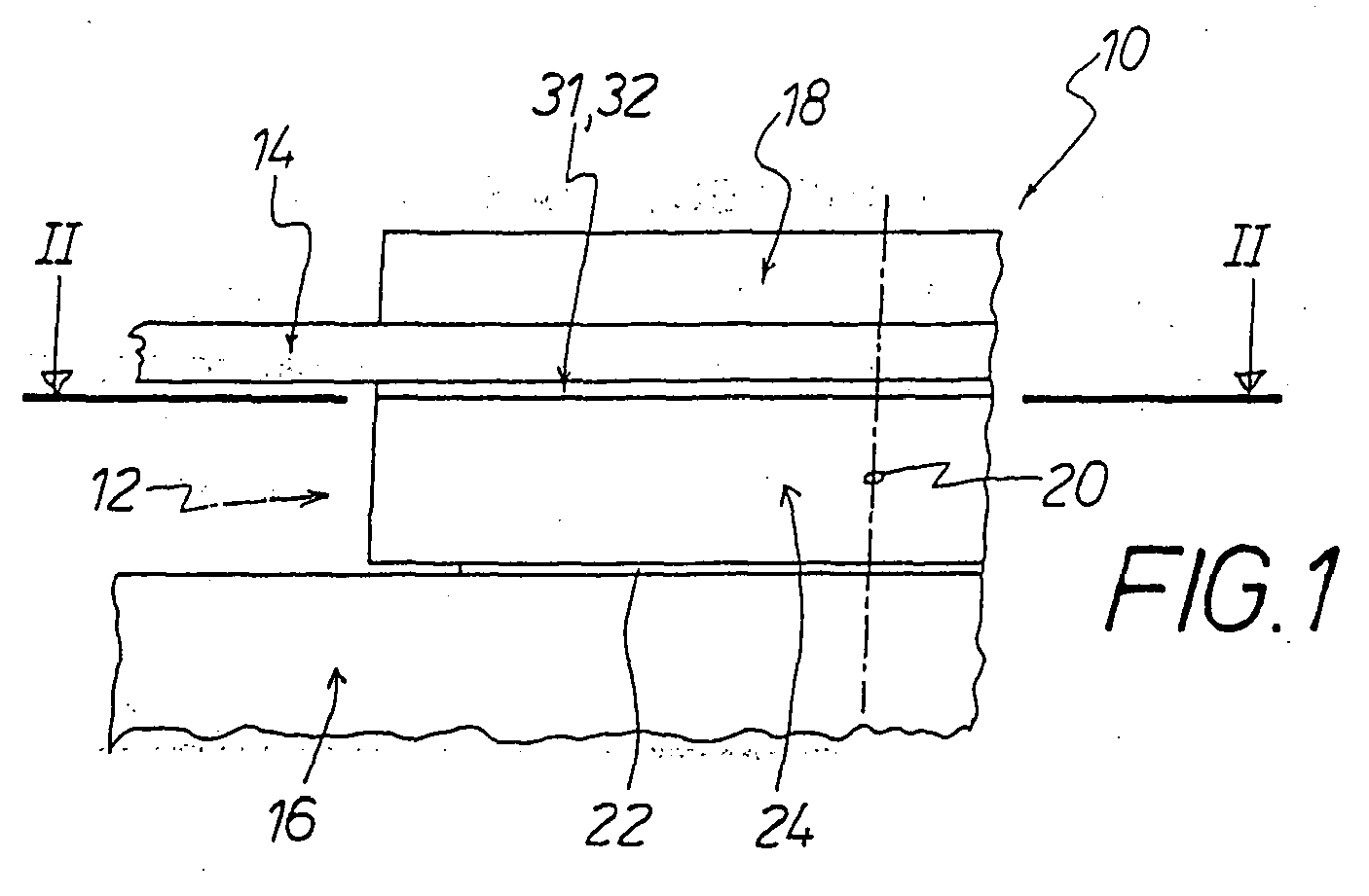
- Figure 1 illustrates schematically cut away in a side view of an embodiment of the circuit arrangement 10 with a power module 12, which is combined with a printed circuit board 14.
- the power module 12 and the printed circuit board 14 are provided between a truncated heat sink 16 and a pressing device 18 and pressure-contacted with each other in a conventional manner.
- the pressing device 18 For pressing the printed circuit board 14 with the power module 12, the pressing device 18 is clamped to the heat sink 16. This bracing takes place, for example, with the aid of at least one screw, which is illustrated schematically in FIG. 1 by a dot-dash line 20.
- the power module 12 has, in a manner known per se, at least one module plate element 22 and a cup-shaped housing 24.
- the cup-shaped housing 24 is formed with shafts 26 (see Figures 2, 3, 4, 10 and 11).
- the shafts 26 are provided for pressure contact elements 28 (see Figures 2, 3, 4, 7 and 11).
- the pressure contact elements 28 serve for the known pressure contact of the at least one module plate element 22 with the printed circuit board 14.
- a seal 31 is provided between the printed circuit board 14 and the base surface 30 of the cup-shaped housing 24 facing it.
- This seal 31 is formed by opening sealing ribs 42 (see Figures 2, 3, 4, 7, 10 and 11), each around orifices 40 of provided for the pressure contact elements 28 shafts 26 are provided around.
- the opening sealing ribs 42 can in each case be assigned to individual shafts 26 (see FIG. 2) or groups of shafts 26 (see FIG.
- the opening sealing ribs 42 lie directly and immediately close to the printed circuit board 14, or a sealing surface element 32 is provided between the printed circuit board 14 and the base 30 of the cup-shaped housing 24 (see Figures 6 to 9).
- the seal 31 between the printed circuit board 14 and the cup-shaped housing 24 of the power module 12 can also be improved by an edge sealing lip 38 (see Figures 2, 3, 5, 6, 10 and 11) surrounding the base edge 30 of the cup-shaped housing 24 be.
- the Abdicht perennialelement 32 is formed with recesses 34 which are provided congruently with the mouth openings 40 of the wells 26 and through which the pressure contact elements 28 extend therethrough and are pressure-contacted with the circuit board 14.
Landscapes
- Engineering & Computer Science (AREA)
- Metallurgy (AREA)
- Manufacturing & Machinery (AREA)
- Microelectronics & Electronic Packaging (AREA)
- Casings For Electric Apparatus (AREA)
- Cooling Or The Like Of Electrical Apparatus (AREA)
- Inverter Devices (AREA)
Abstract
Es wird eine Schaltungsanordnung (10) mit einem Leistungsmodul (12) beschrieben, das mit einer Leiterplatte (14) kombiniert ist. Das Leistungsmodul (12) und die Leiterplatte (14) sind zwischen einem Kühlkörper (16) und einer Presseinrichtung (18) vorgesehen und miteinander durch Druckkontaktelemente (28) kontaktiert. Das Leistungsmodul (12) weist mindestens ein Modul-Plattenelement (22) und ein Gehäuse (24) auf, das mit Schächten (26) für die Druckkontaktelemente (28) ausgebildet ist. Die Schächte (26) münden aus der der Leiterplatte (14) zugewandten Grundfläche (30) des Gehäuses (24) an Mündungsöffnungen (40) aus. Die Grundfläche (30) des Gehäuses (24) ist um die Mündungsöffnungen (40) herum mit Öffnungs-Dichtrippen (42) ausgebildet. Ausserdem kann die Grundfläche (30) des Gehäuses (24) entlang ihres Aussenrandes (36) eine umlaufende Randdichtrippe (38) aufweisen. Ferner kann zwischen der Leiterplatte (14) und der Grundfläche (30) des Gehäuses (24) ein Abdichtflächenelement (32) vorgesehen sein.
Description
Die Erfindung betrifft eine Schaltungsanordnung mit einem Leistungsmodul, das mit einer Leiterplatte kombiniert ist, wobei das Leistungsmodul und die Leiterplatte zwischen einem Kühlkörper und einer Presseinrichtung vorgesehen und miteinander durch Druckkontaktelemente druckkontaktiert sind, wobei das Leistungsmodul mindestens ein Modul-Plattenelement und ein Gehäuse aufweist, das mit Schächten für die Druckkontaktelemente ausgebildet ist, die mit dem mindestens einen Modul-Plattenelement und der Leiterplatte kontaktiert sind, wobei die Schächte aus der der Leiterplatte, zugewandten Grundfläche des Gehäuses an Mündungsöffnungen ausmünden.The invention relates to a circuit arrangement with a power module, which is combined with a printed circuit board, wherein the power module and the printed circuit board between a heat sink and a pressing device provided and pressure-contacted with each other by pressure contact elements, wherein the power module at least one module plate element and a housing which is formed with shafts for the pressure contact elements, which are contacted with the at least one module plate element and the circuit board, wherein the shafts from the circuit board, facing base of the housing open at mouth openings.
Bei derartigen Schaltungsanordnungen kann nicht zuverlässig ausgeschlossen werden, dass es unter extremen Klimabedingungen, wie beispielsweise einer extremen Feuchtebeaufschlagung mit zwischenzeitlicher Betauung, zu einem Ausfall der Schaltungsanordnung kommt. Derartige Ausfälle sind insbesondere durch eine Korrosion des mindestens einen Modul-Plattenelements-des Leistungsmoduls, der Druckkontaktelemente und/oder der Leiterplatte bedingt.In such circuit arrangements can not be reliably ruled out that it comes under extreme climatic conditions, such as an extreme humidity exposure with intermittent condensation, to a failure of the circuit. Such failures are in particular due to corrosion of the at least one module plate element of the power module, the pressure contact elements and / or the circuit board.
Der Erfindung liegt deshalb die Aufgabe zugrunde, eine Schaltungsanordnung der eingangs genannten Art zu schaffen, bei der mit einfachen Mitteln eine Korrosion des Leistungsmoduls, der Druckkontaktelemente und/oder der Leiterplatte verhindert und ein daraus resultierender Ausfall der Schaltungsanordnung vermieden wird.The invention is therefore an object of the invention to provide a circuit arrangement of the type mentioned in which prevents simple means corrosion of the power module, the pressure contact elements and / or the circuit board and a resulting failure of the circuit is avoided.
Diese Aufgabe wird bei einer Schaltungsanordnung der eingangs genannten Art erfindungsgemäss durch die Merkmale des Anspruchs 1, d.h. dadurch gelöst, dass die Grundfläche des Gehäuses um die Mündungsöffnungen der für die Druckkontaktelemente vorgesehenen Schächte herum mit Öffnungs-Dichtrippen ausgebildet ist. Diese Öffnungs-Dichtrippen können einzelnen Mündungsöffnungen oder Gruppen von Mühdungsöffnungen zugeordnet sein.This object is achieved in a circuit arrangement of the type mentioned according to the invention by the features of claim 1, ie, characterized in that the base of the housing is formed around the mouth openings of the provided for the pressure contact elements shafts around with opening sealing ribs. These opening sealing ribs may be associated with individual orifices or groups of orifices.
Durch diese Öffnungs-Dichtrippen ergibt sich der Vorteil, dass ein Eindringen von Feuchtigkeit verhindert und folglich Korrosionen an der Leiterplatte, den Druckkontaktelementen und/oder dem Leistungsmodul vermieden werden.This opening sealing ribs has the advantage that the penetration of moisture is prevented and consequently corrosion on the circuit board, the pressure contact elements and / or the power module are avoided.
Die erfindungsgemässe Schaltungsanordnung besitzt folglich eine optimale Betriebszuverlässigkeit und Lebensdauer.Consequently, the circuit arrangement according to the invention has optimum operating reliability and service life.
Bei der erfindungsgemässen Schaltungsanordnung können die Öffnungs-Dichtrippen aus dem Material des Gehäuses bestehen, d.h. mit dem Gehäuse in einem Herstellungsprozess integral ausgebildet sein. Eine andere Möglichkeit besteht darin, dass die an den Mündungsöffnungen der Grundfläche des Gehäuses vorgesehenen Öffnungs-Dichtrippen aus einem nachgiebigen Material bestehen. Derartige Öffnungs-Dichtrippen der zuletzt genannten Art können beispielsweise auf die Grundfläche des Gehäuses aufgedruckt werden; eine andere Möglichkeit besteht darin, das Gehäuse in einem 2K-Spritzverfahren herzustellen, wobei das Gehäuse aus einem formstabilen harten Material und die Öffnungs-Dichtrippen aus einem nachgiebigen Material bestehen und in einem gemeinsamen Herstellungsprozess an der Grundfläche des Gehäuses bei der Realisierung desselben hergestellt werden.In the inventive circuit arrangement, the opening sealing ribs may be made of the material of the housing, i. be integrally formed with the housing in a manufacturing process. Another possibility is that the openings provided at the mouth openings of the base of the housing opening sealing ribs are made of a resilient material. Such opening sealing ribs of the latter type can be printed, for example, on the base of the housing; Another possibility is to produce the housing in a 2K injection molding process, wherein the housing of a dimensionally stable hard material and the opening sealing ribs made of a resilient material and are manufactured in a common manufacturing process on the base of the housing in the realization of the same.
Unabhängig davon, ob die Öffnungs-Dichtrippen mit dem Gehäusematerial einstückig oder aus einem vom Gehäusematerial verschiedenen, relativ nachgiebigen Material hergestellt werden, ergibt sich durch die den einzelnen Mündungsöffnungen oder Gruppen von Mündungsöffnungen zugeordneten Öffnungs-Dichtrippen eine gute Abdichtung zwischen der Grundfläche des Gehäuses des Leistungsmoduls und der dieser benachbarten LeiterplatteRegardless of whether the opening sealing ribs are made with the housing material in one piece or from a relatively flexible material different from the housing material, resulting from the individual orifices or groups of orifices associated opening sealing ribs a good seal between the Base of the housing of the power module and this adjacent circuit board
Eine weitere Verbesserung der Abdichteigenschaften der erfindungsgemässen Schaltungsanordnung ergibt sich, wenn die Grundfläche des Gehäuses des Leistungsmoduls entlang ihres Aussenrandes eine umlaufende Randdichtrippe aufweist. Diese umlaufende Randdichtrippe kann - wie die Öffnungs-Dichtrippen - aus dem Material des Gehäuses bestehen und mit dem Gehäusematerial einstückig ausgebildet sein, oder die umlaufende Randdichtrippe besteht aus einem nachgiebigen Material und wird am Aussenrand der Grundfläche des Gehäuses des Leistungsmoduls vorgesehen.A further improvement of the sealing properties of the circuit arrangement according to the invention results when the base area of the housing of the power module has a circumferential edge sealing rib along its outer edge. This circumferential edge sealing rib can - like the opening sealing ribs - consist of the material of the housing and be integrally formed with the housing material, or the peripheral edge sealing rib is made of a resilient material and is provided on the outer edge of the base of the housing of the power module.
Bezüglich der umlaufenden Randdichtrippe gelten die oben zu den Öffnungs-Dichtrippen gemachten Ausführungen entsprechend.With regard to the circumferential edge sealing rib, the statements made above with regard to the opening sealing ribs apply correspondingly.
Noch weiter verbesserte Abdichteigenschaften bzw. eine optimale Abdichtung ergibt sich bei der erfindungsgemässen Schaltungsanordnung; wenn zwischen der Leiterplatte und der Grundfläche des Gehäuses ein Abdichtflächenelement vorgesehen ist, das mit Ausnehmungen für die Druckkontaktelemente ausgebildet ist. Das Abdichtflächenelement ist vorzugsweise von einer Kunststofffolie gebildet. Bei dieser Folie kann es sich beispielsweise um eine PTFE-Folie handeln, die im Temperaturbereich zwischen -20 und +260 °C einsetzbar ist, die säure-, laugen-, benzin- und ölbeständig und unbrennbar ist und folglich dem Brandverhalten UL94VO entspricht.Even further improved sealing properties or an optimal sealing results in the inventive circuit arrangement; if between the circuit board and the base of the housing, a Abdichtflächenelement is provided which is formed with recesses for the pressure contact elements. The sealing surface element is preferably formed by a plastic film. This film may, for example, be a PTFE film which can be used in the temperature range between -20 and + 260 ° C., which is resistant to acid, alkali, petrol and oil and incombustible and consequently corresponds to the fire behavior UL94VO.
Selbstverständlich kann das Abdichtflächenelement auch aus einem anderen geeigneten Material bestehen.Of course, the sealing surface may also consist of another suitable material.
Zweckmässigerweise ist das Abdichtflächenelement mit Aussenabmessungen ausgebildet, die den Randabmessungen der Grundfläche des Gehäuses des Leistungsmoduls entsprechen, d.h. die gleich gross oder geringfügig grösser sind als die Grundfläche des Gehäuses.Conveniently, the sealing surface element is formed with external dimensions corresponding to the edge dimensions of the base of the housing of the power module, i. which are equal to or slightly larger than the base of the housing.
Weitere Einzelheiten, Merkmale und Vorteile ergeben sich aus der nachfolgenden Beschreibung eines in der Zeichnung schematisch verdeutlichten Ausführungsbeispiels der erfindungsgemässen Schaltungsanordnung bzw. wesentliche Einzelheiten derselben.Further details, features and advantages will become apparent from the following description of a schematically illustrated in the drawing embodiment of the inventive circuit arrangement or essential details thereof.
- Figur 1FIG. 1
- abschnittweise in einer Seitenansicht nicht massstabgetreu eine Ausführungsform der Schaltungsanordnung,not in scale in a side view to scale an embodiment of the circuit arrangement,
- Figur 2FIG. 2
- eine Ansicht in Blickrichtung der Pfeile II-II in Figur 1 auf einen Abschnitt der Grundfläche des Gehäuses des Leistungsmoduls der Schaltungsanordnung,a view in the direction of arrows II-II in Figure 1 on a portion of the base of the housing of the power module of the circuit arrangement,
- Figur 3FIG. 3
- eine der Figur 2 ähnliche abschnittweise Draufsicht auf eine andere Ausbildung des Gehäuses des Leistungsmoduls der Schaltungsanordnung,FIG. 2 is a partial plan view, similar to FIG. 2, of another embodiment of the housing of the power module of the circuit arrangement;
- Figur 4FIG. 4
- einen Schnitt entlang der Schnittlinie IV-IV in Figur 2 in einem grösseren Massstab,a section along the section line IV-IV in Figure 2 on a larger scale,
- Figur 5FIG. 5
- einen Schnitt entlang der Schnittlinie V-V in Figur 2 in einem grösseren Massstab,3 a section along the section line V-V in FIG. 2 on a larger scale,
- Figur 6FIG. 6
- eine der Figur 5 ähnliche abschnittweise Schnittdarstellung einer anderen Ausbildung der Schaltungsanordnung,5 is a sectional sectional view similar to Figure 5 of another embodiment of the circuit arrangement,
- Figur 7FIG. 7
- eine der Figur 4 ähnliche abschnittweise Schnittdarstellung der Ausbildung der Schaltungsanordnung gemäss Figur 6,4 is a sectional sectional view similar to FIG. 4 of the embodiment of the circuit arrangement according to FIG. 6,
- Figur 8FIG. 8
- eine perspektivische Ansicht eines Abdichtflächenelements einer Schaltungsanordnung gemäss den Figuren 6 und 7,3 is a perspective view of a sealing surface element of a circuit arrangement according to FIGS. 6 and 7,
- Figur 9FIG. 9
- eine Ansicht des Abdichtflächenelements in Blickrichtung von oben,a view of the Abdichtflächenelements seen from above,
- Figur 10FIG. 10
- eine perspektivische Ansicht einer Ausbildung des Gehäuses des Leistungsmoduls der Schaltungsanordnung, unda perspective view of an embodiment of the housing of the power module of the circuit, and
- Figur 11FIG. 11
- eine Ansicht des Gehäuses gemäss Figur 1 in Blickrichtung von oben.a view of the housing according to Figure 1 in the direction of view from above.
Figur 1 verdeutlicht schematisch abgeschnitten in einer Seitenansicht eine Ausbildung der Schaltungsanordnung 10 mit einem Leistungsmodul 12, das mit einer Leiterplatte 14 kombiniert ist. Das Leistungsmodul 12 und die Leiterplatte 14 sind zwischen einem abgeschnitten gezeichneten Kühlkörper 16 und einer Presseinrichtung 18 vorgesehen und miteinander in an sich bekannter Weise druckkontaktiert.Figure 1 illustrates schematically cut away in a side view of an embodiment of the circuit arrangement 10 with a power module 12, which is combined with a printed
Zum Verpressen der Leiterplatte 14 mit dem Leistungsmodul 12 wird die Presseinrichtung 18 mit dem Kühlkörper 16 verspannt. Dieses Verspannen erfolgt beispielsweise mit Hilfe mindestens einer Schraube, die in Figur 1 durch eine strichpunktierte Linie 20 schematisch verdeutlicht ist.For pressing the printed
Das Leistungsmodul 12 weist in an sich bekannter Weise mindestens ein Modul-Plattenelement 22 und ein becherförmiges Gehäuse 24 auf. Das becherförmige Gehäuse 24 ist mit Schächten 26 (sh. die Figuren 2, 3, 4, 10 und 11) ausgebildet. Die Schächte 26 sind für Druckkontaktelemente 28 (sh. die Figuren 2, 3, 4, 7 und 11) vorgesehen. Die Druckkontaktelemente 28 dienen zur an sich bekannten Druckkontaktierung des mindestens einen Modul-Plattenelements 22 mit der Leiterplatte 14.The power module 12 has, in a manner known per se, at least one
Um zwischen dem Leistungsmodul 12 und der Leiterplatte 14 eine zuverlässige Abdichtung gegen das Eindringen von Feuchtigkeit zu bewirken, ist zwischen der Leiterplatte 14 und der dieser zugewandten Grundfläche 30 des becherförmigen Gehäuses 24 eine Abdichtung 31 vorgesehen. Diese Abdichtung 31 ist von Öffnungs-Dichtrippen 42 (sh. die Figuren 2, 3, 4, 7, 10 und 11) gebildet, die jeweils um Mündungsöffnungen 40 der für die Druckkontaktelemente 28 vorgesehenen Schächte 26 herum vorgesehen sind. Die Offnungs-Dichtrippen 42 können dabei jeweils einzelnen Schächten 26 (sh. Figur 2) oder Gruppen von Schächten 26 (sh. Figur 3) zugeordnet sein.In order to effect a reliable seal against the ingress of moisture between the power module 12 and the
Die Öffnungs-Dichtrippen 42 liegen dabei direkt und unmittelbar dicht an der Leiterplatte 14 an, oder es ist zwischen der Leiterplatte 14 und der Grundfläche 30 des becherförmigen Gehäuses 24 ein Abdichtflächenelement 32 vorgesehen (sh. die Figuren 6 bis 9).The opening
Die Abdichtung 31 zwischen der Leiterplatte 14 und dem becherförmigen Gehäuse 24 des Leistungsmoduls 12 kann ausserdem durch eine am Aussenrand 36 der Grundfläche 30 des becherförmigen Gehäuses 24 umlaufende Randdichtlippe 38 (sh. die Figuren 2, 3, 5, 6, 10 und 11) verbessert sein.The seal 31 between the printed
Das Abdichtflächenelement 32 ist mit Ausnehmungen 34 ausgebildet, die mit den Mündungsöffnungen 40 der Schächte 26 deckungsgleich vorgesehen sind und durch die sich die Druckkontaktelemente 28 hindurch erstrecken und mit der Leiterplatte 14 druckkontaktiert sind.The
Gleiche Einzelheiten sind in den Figuren 1 bis 11 jeweils mit denselben Bezugsziffern bezeichnet, so dass es sich erübrigt, in Verbindung mit allen Figuren alle Einzelheiten jeweils detailliert zu beschreiben.The same details are designated by the same reference numerals in FIGS. 1 to 11, so that it is not necessary to describe all details in detail in connection with all figures.
- 1010
- Schaltungsanordnungcircuitry
- 1212
- Leistungsmodule (von 10)Power Modules (out of 10)
- 1414
- Leiterplatte (von 10)Circuit board (from 10)
- 1616
- Kühlkörper (von 10)Heat sink (from 10)
- 1818
- Presseinrichtung (für 12 und 14)Pressing device (for 12 and 14)
- 2020
- strichpunktierte Linie / Schraube (zwischen 18 und 16)dot-dash line / screw (between 18 and 16)
- 2222
- Modul-Plattenelement (von 12)Module plate element (from 12)
- 2424
- becherförmiges Gehäuse (von 12 für 22)cup-shaped case (from 12 to 22)
- 2626
- Schächte (in 24 für 28)Shafts (in 24 for 28)
- 2828
- Druckkontaktelemente (zwischen 12 und 14)Pressure contact elements (between 12 and 14)
- 3030
- Grundfläche (von 24)Footprint (from 24)
- 3131
- Abdichtung (zwischen 14 und 12)Sealing (between 14 and 12)
- 3232
- Abdichtflächenelement (zwischen 12 und 14)Sealing surface element (between 12 and 14)
- 3434
- Ausnehmungen (in 32)Recesses (in 32)
- 3636
- Aussenrand (von 24 bzw. 30)Outside edge (from 24 or 30)
- 3838
- Randdichtrippe (an 36)Edge sealing rib (at 36)
- 4040
- Mündungsöffnungen (von 26 bei 30)Mouth openings (from 26 at 30)
- 4242
- Öffnungs-Dichtrippen (bei 40)Opening sealing ribs (at 40)
Claims (10)
dadurch gekenzeichnet,
dass die Grundfläche (30) des Gehäuses (24) um die Mündungsöffnungen (40) der für die Druckkontaktelemente (28) vorgesehenen Schächte (26) herum mit Öffnungs-Dichtrippen (42) ausgebildet sind.Circuit arrangement (10) having a power module (12) which is combined with a printed circuit board (14), wherein the power module (12) and the printed circuit board (14) between a heat sink (16) and a pressing device (18) and provided by Druckkontaktierungselemente (28) are pressure-contacted, wherein the power module (12) has at least one module plate element (22) and a housing (24) which is formed with shafts (26) for the pressure contact elements (28) with the at least one module Plate element (22) and the printed circuit board (14) are pressure-contacted, wherein the shafts (26) from the circuit board (14) facing base (30) of the housing (24) lead to mouth openings (40),
characterized by
that the base surface (30) of the housing (24) around the Mouth openings (40) of the pressure contact elements (28) provided for shafts (26) around with opening sealing ribs (42) are formed.
dadurch gekennzeichnet,
dass die Öffnungs-Dichtrippen (42) einzelnen Mündungsöffnungen (40) und/oder Gruppen von Mündungsöffnungen (40) zugeordnet sind.Circuit arrangement according to Claim 1,
characterized,
that the opening-sealing ribs are associated (42) individual outlet openings (40) and / or groups of discharge openings (40).
dadurch gekennzeichnet,
dass die Öffnungs-Dichtrippen (42) aus dem Material des becherförmigen Gehäuses (24) bestehen und mit dem becherförmigen Gehäuse (24) material-einstückig ausgebildet sind.Circuit arrangement according to Claim 1 or 2,
characterized,
in that the opening sealing ribs (42) consist of the material of the cup-shaped housing (24) and are formed in one piece with the cup-shaped housing (24).
dadurch gekennzeichnet,
dass die Öffnungs-Dichtrippen (42) aus einem nachgiebigen Material bestehen und an den Mündungsöffnungen (40) der Grundfläche (30) des becherförmigen Gehäuses (24) vorgesehen sind.Circuit arrangement according to Claim 1 or 2,
characterized,
in that the opening sealing ribs (42) consist of a resilient material and are provided on the mouth openings (40) of the base surface (30) of the cup-shaped housing (24).
dadurch gekennzeichnet,
dass die Grundfläche (30) des becherförmigen Gehäuses (24) entlang ihres. Aussenrandes (36) eine umlaufende Randdichtrippe (38) aufweist.Circuit arrangement according to one of Claims 1 to 4,
characterized,
that the base surface (30) of the cup-shaped housing (24) along its. Outside edge (36) has a circumferential edge sealing rib (38).
dadurch gekennzeichnet,
dass die umlaufende Randdichtrippe (38) aus dem Material des becherförmigen Gehäuses (24) besteht und mit dem becherförmigen Gehäuse (24) material-einstückig ausgebildet ist.Circuit arrangement according to Claim 5,
characterized,
in that the peripheral edge sealing rib (38) consists of the material of the cup-shaped housing (24) and is integrally formed with the cup-shaped housing (24).
dadurch gekennzeichnet,
dass die umlaufende Randdichtrippe (38) aus einem nachgiebigen Material besteht und am Aussenrand (36) der Grundfläche (30) des becherförmigen Gehäuses (24) vorgesehen ist.Circuit arrangement according to Claim 5,
characterized,
in that the peripheral edge sealing rib (38) consists of a resilient material and is provided on the outer edge (36) of the base surface (30) of the cup-shaped housing (24).
dadurch gekennzeichnet,
dass zwischen der Leiterplatte (14) und der Grundfläche (30) des becherförmigen Gehäuses (24) ein Abdichtflächenelement (32) vorgesehen ist, das mit Ausnehmungen (34) für die Druckkontaktelemente (28) ausgebildet ist.Circuit arrangement according to one of Claims 1 to 7,
characterized,
in that a sealing surface element (32), which is formed with recesses (34) for the pressure contact elements (28), is provided between the printed circuit board (14) and the base surface (30) of the cup-shaped housing (24).
dadurch gekennzeichnet,
dass das Abdichtflächenelement (32) Aussenabmessungen aufweist, die den Randabmessungen der Grundfläche (30) des becherförmigen Gehäuses (24) entsprechen.Circuit arrangement according to Claim 8,
characterized,
in that the sealing surface element (32) has external dimensions which correspond to the edge dimensions of the base surface (30) of the cup-shaped housing (24).
dadurch gekennzeichnet
dass das Abdichtflächenelement (32) von einer Kunststofffolie gebildet ist.Circuit arrangement according to Claim 8,
characterized
in that the sealing surface element (32) is formed by a plastic film.
Applications Claiming Priority (1)
| Application Number | Priority Date | Filing Date | Title |
|---|---|---|---|
| DE200610052619 DE102006052619B4 (en) | 2006-11-08 | 2006-11-08 | Circuit arrangement with a power module that is combined with a printed circuit board |
Publications (3)
| Publication Number | Publication Date |
|---|---|
| EP1921908A2 true EP1921908A2 (en) | 2008-05-14 |
| EP1921908A3 EP1921908A3 (en) | 2009-12-02 |
| EP1921908B1 EP1921908B1 (en) | 2012-08-01 |
Family
ID=39056377
Family Applications (1)
| Application Number | Title | Priority Date | Filing Date |
|---|---|---|---|
| EP20070021363 Active EP1921908B1 (en) | 2006-11-08 | 2007-11-02 | Circuit assembly with a power module that is combined with a circuit board |
Country Status (4)
| Country | Link |
|---|---|
| EP (1) | EP1921908B1 (en) |
| JP (1) | JP5183148B2 (en) |
| DE (1) | DE102006052619B4 (en) |
| DK (1) | DK1921908T3 (en) |
Cited By (1)
| Publication number | Priority date | Publication date | Assignee | Title |
|---|---|---|---|---|
| GB2547087A (en) * | 2015-12-17 | 2017-08-09 | Bosch Gmbh Robert | Converter circuit |
Families Citing this family (3)
| Publication number | Priority date | Publication date | Assignee | Title |
|---|---|---|---|---|
| JP6355994B2 (en) * | 2014-07-09 | 2018-07-11 | 株式会社ユーシン | Waterproof structure of control device |
| DE102014227024A1 (en) | 2014-12-30 | 2016-06-30 | Robert Bosch Gmbh | power device |
| DE102014227027B4 (en) | 2014-12-30 | 2026-01-22 | Robert Bosch Gmbh | Power semiconductor control and converter, transformer and device including these |
Family Cites Families (6)
| Publication number | Priority date | Publication date | Assignee | Title |
|---|---|---|---|---|
| DE19630173C2 (en) * | 1996-07-26 | 2001-02-08 | Semikron Elektronik Gmbh | Power module with semiconductor components |
| JP3476142B2 (en) * | 2001-05-24 | 2003-12-10 | 日本電気株式会社 | Electronic device with dew condensation prevention structure |
| US6417747B1 (en) * | 2001-08-23 | 2002-07-09 | Raytheon Company | Low cost, large scale RF hybrid package for simple assembly onto mixed signal printed wiring boards |
| JP4186826B2 (en) * | 2004-01-28 | 2008-11-26 | 株式会社デンソー | PCB mounting structure |
| DE102005024900B4 (en) * | 2004-06-08 | 2012-08-16 | Fuji Electric Co., Ltd. | power module |
| JP4764979B2 (en) * | 2004-06-08 | 2011-09-07 | 富士電機株式会社 | Semiconductor device |
-
2006
- 2006-11-08 DE DE200610052619 patent/DE102006052619B4/en active Active
-
2007
- 2007-10-25 JP JP2007277608A patent/JP5183148B2/en active Active
- 2007-11-02 EP EP20070021363 patent/EP1921908B1/en active Active
- 2007-11-02 DK DK07021363T patent/DK1921908T3/en active
Cited By (1)
| Publication number | Priority date | Publication date | Assignee | Title |
|---|---|---|---|---|
| GB2547087A (en) * | 2015-12-17 | 2017-08-09 | Bosch Gmbh Robert | Converter circuit |
Also Published As
| Publication number | Publication date |
|---|---|
| JP2008124456A (en) | 2008-05-29 |
| EP1921908B1 (en) | 2012-08-01 |
| EP1921908A3 (en) | 2009-12-02 |
| JP5183148B2 (en) | 2013-04-17 |
| DK1921908T3 (en) | 2012-10-22 |
| DE102006052619B4 (en) | 2009-07-30 |
| DE102006052619A1 (en) | 2008-05-15 |
Similar Documents
| Publication | Publication Date | Title |
|---|---|---|
| EP1921910B1 (en) | Circuit with a power module that is combined with a circuit board | |
| DE69425705T3 (en) | position sensors | |
| DE102008017809B4 (en) | The power semiconductor module | |
| DE102008020668A1 (en) | Plug connection for contacting an electrical circuit board arranged in a housing | |
| DE102021109282B4 (en) | Battery module for a motor vehicle | |
| EP1921908A2 (en) | Circuit assembly with a power module that is combined with a circuit board | |
| DE102008014457A1 (en) | Transmission control device for motor vehicle, has contact structures connected with each other by interface in mounted condition of two electrical components, where one component is provided with controller and other with sensor unit | |
| EP2305010A1 (en) | Electrical circuit arrangement | |
| WO2015014509A1 (en) | Multi-stage sealing system for use in a motor vehicle control unit | |
| WO2003075626A1 (en) | Heat dissipating device for dissipating heat generated by an electrical component | |
| DE102004007230B4 (en) | Housing with liquid-tight electrical feedthrough | |
| DE102020000632A1 (en) | poetry | |
| DE102021101895B4 (en) | Semiconductor device and method for manufacturing the same | |
| DE202022103899U1 (en) | Cell contact system and energy storage | |
| DE102016214329A1 (en) | A valve block assembly | |
| DE60113050T2 (en) | Seal of a vehicle door interior panel with a Gehaüsestecker | |
| DE102017214242A1 (en) | Battery cell, battery module and method of making such | |
| EP2148368A1 (en) | High performance semiconductor module | |
| DE19541217A1 (en) | Lamp with housing and seal formed together in injection moulding process | |
| DE102019219560A1 (en) | Housing for at least one electronic component | |
| DE112020004805T5 (en) | CONNECTOR CONNECTION STRUCTURE | |
| DE102013223479A1 (en) | Housing for a transmission control | |
| DE102017204924A1 (en) | ELECTRONIC CONTROL UNIT | |
| DE3215320C2 (en) | ||
| DE102015017297B4 (en) | Fusible link and connection arrangement with such a fuse |
Legal Events
| Date | Code | Title | Description |
|---|---|---|---|
| PUAI | Public reference made under article 153(3) epc to a published international application that has entered the european phase |
Free format text: ORIGINAL CODE: 0009012 |
|
| AK | Designated contracting states |
Kind code of ref document: A2 Designated state(s): AT BE BG CH CY CZ DE DK EE ES FI FR GB GR HU IE IS IT LI LT LU LV MC MT NL PL PT RO SE SI SK TR |
|
| AX | Request for extension of the european patent |
Extension state: AL BA HR MK RS |
|
| PUAL | Search report despatched |
Free format text: ORIGINAL CODE: 0009013 |
|
| AK | Designated contracting states |
Kind code of ref document: A3 Designated state(s): AT BE BG CH CY CZ DE DK EE ES FI FR GB GR HU IE IS IT LI LT LU LV MC MT NL PL PT RO SE SI SK TR |
|
| AX | Request for extension of the european patent |
Extension state: AL BA HR MK RS |
|
| 17P | Request for examination filed |
Effective date: 20091105 |
|
| 17Q | First examination report despatched |
Effective date: 20091211 |
|
| AKX | Designation fees paid |
Designated state(s): AT BE BG CH CY CZ DE DK EE ES FI FR GB GR HU IE IS IT LI LT LU LV MC MT NL PL PT RO SE SI SK TR |
|
| REG | Reference to a national code |
Ref country code: DE Ref legal event code: R079 Ref document number: 502007010290 Country of ref document: DE Free format text: PREVIOUS MAIN CLASS: H05K0007140000 Ipc: H05K0001110000 |
|
| GRAP | Despatch of communication of intention to grant a patent |
Free format text: ORIGINAL CODE: EPIDOSNIGR1 |
|
| RIC1 | Information provided on ipc code assigned before grant |
Ipc: H05K 7/14 20060101ALI20120420BHEP Ipc: H05K 1/11 20060101AFI20120420BHEP Ipc: H05K 3/32 20060101ALI20120420BHEP |
|
| GRAS | Grant fee paid |
Free format text: ORIGINAL CODE: EPIDOSNIGR3 |
|
| GRAA | (expected) grant |
Free format text: ORIGINAL CODE: 0009210 |
|
| AK | Designated contracting states |
Kind code of ref document: B1 Designated state(s): AT BE BG CH CY CZ DE DK EE ES FI FR GB GR HU IE IS IT LI LT LU LV MC MT NL PL PT RO SE SI SK TR |
|
| REG | Reference to a national code |
Ref country code: GB Ref legal event code: FG4D Free format text: NOT ENGLISH |
|
| REG | Reference to a national code |
Ref country code: CH Ref legal event code: EP Ref country code: AT Ref legal event code: REF Ref document number: 569229 Country of ref document: AT Kind code of ref document: T Effective date: 20120815 |
|
| REG | Reference to a national code |
Ref country code: IE Ref legal event code: FG4D Free format text: LANGUAGE OF EP DOCUMENT: GERMAN |
|
| REG | Reference to a national code |
Ref country code: DE Ref legal event code: R096 Ref document number: 502007010290 Country of ref document: DE Effective date: 20120927 |
|
| REG | Reference to a national code |
Ref country code: DK Ref legal event code: T3 |
|
| REG | Reference to a national code |
Ref country code: NL Ref legal event code: VDEP Effective date: 20120801 |
|
| REG | Reference to a national code |
Ref country code: SK Ref legal event code: T3 Ref document number: E 12746 Country of ref document: SK |
|
| REG | Reference to a national code |
Ref country code: LT Ref legal event code: MG4D Effective date: 20120801 |
|
| PG25 | Lapsed in a contracting state [announced via postgrant information from national office to epo] |
Ref country code: LT Free format text: LAPSE BECAUSE OF FAILURE TO SUBMIT A TRANSLATION OF THE DESCRIPTION OR TO PAY THE FEE WITHIN THE PRESCRIBED TIME-LIMIT Effective date: 20120801 Ref country code: IS Free format text: LAPSE BECAUSE OF FAILURE TO SUBMIT A TRANSLATION OF THE DESCRIPTION OR TO PAY THE FEE WITHIN THE PRESCRIBED TIME-LIMIT Effective date: 20121201 Ref country code: FI Free format text: LAPSE BECAUSE OF FAILURE TO SUBMIT A TRANSLATION OF THE DESCRIPTION OR TO PAY THE FEE WITHIN THE PRESCRIBED TIME-LIMIT Effective date: 20120801 Ref country code: CY Free format text: LAPSE BECAUSE OF FAILURE TO SUBMIT A TRANSLATION OF THE DESCRIPTION OR TO PAY THE FEE WITHIN THE PRESCRIBED TIME-LIMIT Effective date: 20120801 |
|
| PG25 | Lapsed in a contracting state [announced via postgrant information from national office to epo] |
Ref country code: SI Free format text: LAPSE BECAUSE OF FAILURE TO SUBMIT A TRANSLATION OF THE DESCRIPTION OR TO PAY THE FEE WITHIN THE PRESCRIBED TIME-LIMIT Effective date: 20120801 Ref country code: GR Free format text: LAPSE BECAUSE OF FAILURE TO SUBMIT A TRANSLATION OF THE DESCRIPTION OR TO PAY THE FEE WITHIN THE PRESCRIBED TIME-LIMIT Effective date: 20121102 Ref country code: PT Free format text: LAPSE BECAUSE OF FAILURE TO SUBMIT A TRANSLATION OF THE DESCRIPTION OR TO PAY THE FEE WITHIN THE PRESCRIBED TIME-LIMIT Effective date: 20121203 Ref country code: PL Free format text: LAPSE BECAUSE OF FAILURE TO SUBMIT A TRANSLATION OF THE DESCRIPTION OR TO PAY THE FEE WITHIN THE PRESCRIBED TIME-LIMIT Effective date: 20120801 Ref country code: SE Free format text: LAPSE BECAUSE OF FAILURE TO SUBMIT A TRANSLATION OF THE DESCRIPTION OR TO PAY THE FEE WITHIN THE PRESCRIBED TIME-LIMIT Effective date: 20120801 Ref country code: LV Free format text: LAPSE BECAUSE OF FAILURE TO SUBMIT A TRANSLATION OF THE DESCRIPTION OR TO PAY THE FEE WITHIN THE PRESCRIBED TIME-LIMIT Effective date: 20120801 |
|
| PG25 | Lapsed in a contracting state [announced via postgrant information from national office to epo] |
Ref country code: NL Free format text: LAPSE BECAUSE OF FAILURE TO SUBMIT A TRANSLATION OF THE DESCRIPTION OR TO PAY THE FEE WITHIN THE PRESCRIBED TIME-LIMIT Effective date: 20120801 |
|
| PG25 | Lapsed in a contracting state [announced via postgrant information from national office to epo] |
Ref country code: EE Free format text: LAPSE BECAUSE OF FAILURE TO SUBMIT A TRANSLATION OF THE DESCRIPTION OR TO PAY THE FEE WITHIN THE PRESCRIBED TIME-LIMIT Effective date: 20120801 Ref country code: CZ Free format text: LAPSE BECAUSE OF FAILURE TO SUBMIT A TRANSLATION OF THE DESCRIPTION OR TO PAY THE FEE WITHIN THE PRESCRIBED TIME-LIMIT Effective date: 20120801 Ref country code: RO Free format text: LAPSE BECAUSE OF FAILURE TO SUBMIT A TRANSLATION OF THE DESCRIPTION OR TO PAY THE FEE WITHIN THE PRESCRIBED TIME-LIMIT Effective date: 20120801 Ref country code: ES Free format text: LAPSE BECAUSE OF FAILURE TO SUBMIT A TRANSLATION OF THE DESCRIPTION OR TO PAY THE FEE WITHIN THE PRESCRIBED TIME-LIMIT Effective date: 20121112 |
|
| BERE | Be: lapsed |
Owner name: SEMIKRON ELEKTRONIK G.M.B.H. & CO. KG Effective date: 20121130 |
|
| PG25 | Lapsed in a contracting state [announced via postgrant information from national office to epo] |
Ref country code: IT Free format text: LAPSE BECAUSE OF FAILURE TO SUBMIT A TRANSLATION OF THE DESCRIPTION OR TO PAY THE FEE WITHIN THE PRESCRIBED TIME-LIMIT Effective date: 20120801 |
|
| PLBE | No opposition filed within time limit |
Free format text: ORIGINAL CODE: 0009261 |
|
| STAA | Information on the status of an ep patent application or granted ep patent |
Free format text: STATUS: NO OPPOSITION FILED WITHIN TIME LIMIT |
|
| REG | Reference to a national code |
Ref country code: CH Ref legal event code: PL |
|
| 26N | No opposition filed |
Effective date: 20130503 |
|
| PG25 | Lapsed in a contracting state [announced via postgrant information from national office to epo] |
Ref country code: CH Free format text: LAPSE BECAUSE OF NON-PAYMENT OF DUE FEES Effective date: 20121130 Ref country code: BG Free format text: LAPSE BECAUSE OF FAILURE TO SUBMIT A TRANSLATION OF THE DESCRIPTION OR TO PAY THE FEE WITHIN THE PRESCRIBED TIME-LIMIT Effective date: 20121101 Ref country code: LI Free format text: LAPSE BECAUSE OF NON-PAYMENT OF DUE FEES Effective date: 20121130 |
|
| REG | Reference to a national code |
Ref country code: IE Ref legal event code: MM4A |
|
| REG | Reference to a national code |
Ref country code: DE Ref legal event code: R097 Ref document number: 502007010290 Country of ref document: DE Effective date: 20130503 |
|
| PG25 | Lapsed in a contracting state [announced via postgrant information from national office to epo] |
Ref country code: BE Free format text: LAPSE BECAUSE OF NON-PAYMENT OF DUE FEES Effective date: 20121130 |
|
| PG25 | Lapsed in a contracting state [announced via postgrant information from national office to epo] |
Ref country code: IE Free format text: LAPSE BECAUSE OF NON-PAYMENT OF DUE FEES Effective date: 20121102 |
|
| PG25 | Lapsed in a contracting state [announced via postgrant information from national office to epo] |
Ref country code: MT Free format text: LAPSE BECAUSE OF FAILURE TO SUBMIT A TRANSLATION OF THE DESCRIPTION OR TO PAY THE FEE WITHIN THE PRESCRIBED TIME-LIMIT Effective date: 20120801 |
|
| REG | Reference to a national code |
Ref country code: AT Ref legal event code: MM01 Ref document number: 569229 Country of ref document: AT Kind code of ref document: T Effective date: 20121130 |
|
| PG25 | Lapsed in a contracting state [announced via postgrant information from national office to epo] |
Ref country code: AT Free format text: LAPSE BECAUSE OF NON-PAYMENT OF DUE FEES Effective date: 20121130 |
|
| PG25 | Lapsed in a contracting state [announced via postgrant information from national office to epo] |
Ref country code: MC Free format text: LAPSE BECAUSE OF NON-PAYMENT OF DUE FEES Effective date: 20121130 Ref country code: TR Free format text: LAPSE BECAUSE OF FAILURE TO SUBMIT A TRANSLATION OF THE DESCRIPTION OR TO PAY THE FEE WITHIN THE PRESCRIBED TIME-LIMIT Effective date: 20120801 |
|
| PG25 | Lapsed in a contracting state [announced via postgrant information from national office to epo] |
Ref country code: LU Free format text: LAPSE BECAUSE OF NON-PAYMENT OF DUE FEES Effective date: 20121102 |
|
| PG25 | Lapsed in a contracting state [announced via postgrant information from national office to epo] |
Ref country code: HU Free format text: LAPSE BECAUSE OF FAILURE TO SUBMIT A TRANSLATION OF THE DESCRIPTION OR TO PAY THE FEE WITHIN THE PRESCRIBED TIME-LIMIT Effective date: 20071102 |
|
| REG | Reference to a national code |
Ref country code: FR Ref legal event code: PLFP Year of fee payment: 9 |
|
| REG | Reference to a national code |
Ref country code: FR Ref legal event code: PLFP Year of fee payment: 10 |
|
| PGFP | Annual fee paid to national office [announced via postgrant information from national office to epo] |
Ref country code: DK Payment date: 20161124 Year of fee payment: 10 Ref country code: SK Payment date: 20161026 Year of fee payment: 10 |
|
| REG | Reference to a national code |
Ref country code: FR Ref legal event code: PLFP Year of fee payment: 11 |
|
| REG | Reference to a national code |
Ref country code: DK Ref legal event code: EBP Effective date: 20171130 |
|
| PG25 | Lapsed in a contracting state [announced via postgrant information from national office to epo] |
Ref country code: SK Free format text: LAPSE BECAUSE OF NON-PAYMENT OF DUE FEES Effective date: 20171102 |
|
| REG | Reference to a national code |
Ref country code: SK Ref legal event code: MM4A Ref document number: E 12746 Country of ref document: SK Effective date: 20171102 |
|
| PG25 | Lapsed in a contracting state [announced via postgrant information from national office to epo] |
Ref country code: DK Free format text: LAPSE BECAUSE OF NON-PAYMENT OF DUE FEES Effective date: 20171130 |
|
| REG | Reference to a national code |
Ref country code: DE Ref legal event code: R081 Ref document number: 502007010290 Country of ref document: DE Owner name: SEMIKRON DANFOSS ELEKTRONIK GMBH & CO. KG, DE Free format text: FORMER OWNER: SEMIKRON ELEKTRONIK GMBH & CO. KG, 90431 NUERNBERG, DE |
|
| PGFP | Annual fee paid to national office [announced via postgrant information from national office to epo] |
Ref country code: DE Payment date: 20251007 Year of fee payment: 19 |
|
| PGFP | Annual fee paid to national office [announced via postgrant information from national office to epo] |
Ref country code: GB Payment date: 20251016 Year of fee payment: 19 |
|
| PGFP | Annual fee paid to national office [announced via postgrant information from national office to epo] |
Ref country code: FR Payment date: 20251008 Year of fee payment: 19 |