EP1921651A2 - Sealing device and method of manufacturing display device using the same - Google Patents
Sealing device and method of manufacturing display device using the same Download PDFInfo
- Publication number
- EP1921651A2 EP1921651A2 EP07120244A EP07120244A EP1921651A2 EP 1921651 A2 EP1921651 A2 EP 1921651A2 EP 07120244 A EP07120244 A EP 07120244A EP 07120244 A EP07120244 A EP 07120244A EP 1921651 A2 EP1921651 A2 EP 1921651A2
- Authority
- EP
- European Patent Office
- Prior art keywords
- region
- substrate
- sealing material
- patterns
- transmission portion
- Prior art date
- Legal status (The legal status is an assumption and is not a legal conclusion. Google has not performed a legal analysis and makes no representation as to the accuracy of the status listed.)
- Granted
Links
Images


Classifications
-
- H—ELECTRICITY
- H05—ELECTRIC TECHNIQUES NOT OTHERWISE PROVIDED FOR
- H05B—ELECTRIC HEATING; ELECTRIC LIGHT SOURCES NOT OTHERWISE PROVIDED FOR; CIRCUIT ARRANGEMENTS FOR ELECTRIC LIGHT SOURCES, IN GENERAL
- H05B33/00—Electroluminescent light sources
- H05B33/02—Details
- H05B33/04—Sealing arrangements, e.g. against humidity
-
- H—ELECTRICITY
- H01—ELECTRIC ELEMENTS
- H01J—ELECTRIC DISCHARGE TUBES OR DISCHARGE LAMPS
- H01J9/00—Apparatus or processes specially adapted for the manufacture, installation, removal, maintenance of electric discharge tubes, discharge lamps, or parts thereof; Recovery of material from discharge tubes or lamps
- H01J9/24—Manufacture or joining of vessels, leading-in conductors or bases
- H01J9/26—Sealing together parts of vessels
- H01J9/261—Sealing together parts of vessels the vessel being for a flat panel display
-
- B—PERFORMING OPERATIONS; TRANSPORTING
- B32—LAYERED PRODUCTS
- B32B—LAYERED PRODUCTS, i.e. PRODUCTS BUILT-UP OF STRATA OF FLAT OR NON-FLAT, e.g. CELLULAR OR HONEYCOMB, FORM
- B32B38/00—Ancillary operations in connection with laminating processes
- B32B38/0008—Electrical discharge treatment, e.g. corona, plasma treatment; wave energy or particle radiation
-
- H—ELECTRICITY
- H01—ELECTRIC ELEMENTS
- H01J—ELECTRIC DISCHARGE TUBES OR DISCHARGE LAMPS
- H01J17/00—Gas-filled discharge tubes with solid cathode
- H01J17/02—Details
- H01J17/18—Seals between parts of vessels; Seals for leading-in conductors; Leading-in conductors
-
- H—ELECTRICITY
- H01—ELECTRIC ELEMENTS
- H01J—ELECTRIC DISCHARGE TUBES OR DISCHARGE LAMPS
- H01J2209/00—Apparatus and processes for manufacture of discharge tubes
- H01J2209/26—Sealing parts of the vessel to provide a vacuum enclosure
-
- H—ELECTRICITY
- H10—SEMICONDUCTOR DEVICES; ELECTRIC SOLID-STATE DEVICES NOT OTHERWISE PROVIDED FOR
- H10K—ORGANIC ELECTRIC SOLID-STATE DEVICES
- H10K50/00—Organic light-emitting devices
- H10K50/80—Constructional details
- H10K50/84—Passivation; Containers; Encapsulations
- H10K50/842—Containers
- H10K50/8426—Peripheral sealing arrangements, e.g. adhesives, sealants
-
- H—ELECTRICITY
- H10—SEMICONDUCTOR DEVICES; ELECTRIC SOLID-STATE DEVICES NOT OTHERWISE PROVIDED FOR
- H10K—ORGANIC ELECTRIC SOLID-STATE DEVICES
- H10K59/00—Integrated devices, or assemblies of multiple devices, comprising at least one organic light-emitting element covered by group H10K50/00
- H10K59/10—OLED displays
- H10K59/12—Active-matrix OLED [AMOLED] displays
-
- H—ELECTRICITY
- H10—SEMICONDUCTOR DEVICES; ELECTRIC SOLID-STATE DEVICES NOT OTHERWISE PROVIDED FOR
- H10K—ORGANIC ELECTRIC SOLID-STATE DEVICES
- H10K59/00—Integrated devices, or assemblies of multiple devices, comprising at least one organic light-emitting element covered by group H10K50/00
- H10K59/80—Constructional details
- H10K59/87—Passivation; Containers; Encapsulations
- H10K59/871—Self-supporting sealing arrangements
- H10K59/8722—Peripheral sealing arrangements, e.g. adhesives, sealants
Definitions
- the present invention relates to a sealing device and a method of manufacturing a display device using the sealing device, and more particularly to a sealing device including a mask for partially irradiating light and a method of manufacturing a display device using the sealing device.
- an organic light display device includes a substrate provided a pixel region and a non-pixel region, and a container or a substrate disposed opposite to the substrate for encapsulation and adhered to the substrate by a sealant such as epoxy.
- a plurality of light emitting devices connected between a scan line and a date line in the form of matrix are formed in the pixel region of the substrate, and the light emitting device includes an anode electrode and a cathode electrode, and an organic thin film layer formed between the anode electrode and the cathode electrode and having a hole transportation layer, an organic light emitting layer, and an electron transportation layer.
- the light emitting device is vulnerable to hydrogen and oxygen since it contains an organic material and is easily oxidized by moisture in air so that the electrical and light emitting characteristic thereof are deteriorated since the cathode electrode is formed of a metal material.
- moisture penetrating from outside is removed by mounting a moisture absorbing material to a container in the form of a can or a cup of a metal material or a substrate of glass or plastic in the form of powder or by bonding the container or the substrate in the form of a film.
- the method of mounting the moisture absorbing material in the form of powder complicates the process and increases the material and process costs, thereby increasing the thickness of the display device. So, it is difficult to apply the method to entire surface light emission. Further, the method of bonding a moisture absorbing material in the form of a film can limitedly remove moisture and has low durability and reliability, thereby making mass-production difficult.
- Korean Patent Laid-Open No. 2001-0084380 (September 6, 2001 ) discloses a method for sealing a frit frame using laser.
- Korean Patent Laid-Open No. 2002-0051153 discloses a packaging method for attaching an upper substrate and a lower substrate to a frit layer using laser.
- FIG. 2 is an enlarged plan view photographed after laser is irradiated to the sealing material.
- the bonding state of the sealing material and the substrate is represented by the differences of lightness and shading. More particularly, a central portion in which the sealing material and the substrate are properly bonded by sufficient energy is bright, and both side portions in which the sealing material and the substrate are incompletely bonded by relatively low energy are dark.
- certain inventive aspects provide a sealing device capable of uniformly bonding a sealing material and a substrate.
- One inventive aspect is a method of manufacturing a display device using a sealing device capable of improving the sealing effect and the reliability by uniformly bonding a sealing material and a substrate.
- One aspect of the invention is a sealing device for bonding a first substrate and a second substrate by interposing a sealing material along edges of the first substrate and the second substrate and by irradiating light to the sealing material.
- the sealing device comprises: a mask, disposed on the second substrate stacked on the first substrate, comprising a transmission portion formed in correspondence to the sealing material; and an optical head irradiating the light to the sealing material through the transmission portion of the mask.
- the transmission portion of the mask comprises a plurality of patterns for regulating the light irradiated to the sealing material.
- the transmission portion of the mask can comprise a plurality of regions having patterns with different transmittances.
- the plurality of patterns can be aligned with at least of a part of the sealing material.
- the energy distribution of the light across the sealing material can be controlled by the plurality of patterns.
- the transmission portion can comprise a first region at a central portion thereof and a second region on both sides of the first region, and the transmittances of the patterns in the first region and the second region can be different.
- the transmittance of the pattern in the first region can be lower than that of the second region.
- the pattern can comprise a plurality of opaque lines, and the transmittance can be controlled by density of the opaque lines of the patterns.
- the opaque lines are arranged parallel to each other and equidistant from each other.
- the transmission portion can comprise a first region on an inner side of a curved corner potion and a second region on an outer side of the curved corner portion and the transmittances of the patterns of the first region and the second region are different.
- the transmittance of the pattern in the first region can be lower than that of the second region.
- the transmission portion can comprise a first region at a central portion, a second region provided on both sides of the first region, and a third region provided on both outer sides of the second region, and the transmittances of the patterns of the first region, the second region, and the third region can be different.
- the first, second, and third regions can comprise line-shaped patterns comprising a plurality of opaque lines, and the transmittance can be controlled by density of the opaque lines of the patterns.
- the light can comprise one of laser and infrared ray.
- the device can further comprise a stage on which the first and second substrates interposing the sealing material in between are mounted.
- Other aspect of the invention provides a method of manufacturing a display device having first and second substrates and a sealing material.
- the method comprises: irradiating light through a mask located on the second substrate; regulating the energy profile of the light irradiated across the sealing material interposed between the first and second substrates using the mask; and bonding the sealing material to the first substrate and the second substrate.
- the regulating the energy profile of the light can comprise passing the light through a mask having a transmission portion.
- the transmission portion can comprise a plurality of regions having pattern with different transmittances.
- the transmission portion can comprise a first region at a central portion thereof and a second region on both sides of the first region, and wherein the transmittances of the patterns in the first region and the second region are different.
- the density of the pattern in the first region can be lower than that of the second region.
- the transmission portion may a first region on an inner side of a curved corner portion and a second region on an outer side of the curved corner portion and the transmittances of the patterns of the first region and the second region may be different.
- the density of the pattern in the first region is lower than that of the pattern in the second region.
- each of the plurality of patterns comprises a plurality of opaque lines, and the transmittance is controlled by density of the opaque lines of the patterns.
- the light may comprise laser and infrared ray.
- the display device comprises an organic light emitting display device.
- the method can further comprise, prior to irradiating: mounting a first substrate and a second substrate to a stage by disposing the first substrate and the second substrate so as to be opposite to each other, with a sealing material being located between the first substrate and the second substrate; and locating the mask in which a transmission portion is formed at a plurality of portions corresponding to the formed sealing material and a plurality of patterns are formed at the transmission portion.
- a sealing device used to bond a first substrate and a second substrate by interposing a sealing material at edges of the first substrate and the second substrate opposite to each other and by irradiating light to the sealing material comprises: a stage to which the first substrate and the second substrate between which the sealing material is interposed is mounted; a mask disposed on one side of the stage, in which a transmission portion is formed in correspondence to the formation position of the sealing member so that light can be irradiated to the sealing material; and an optical head irradiating the light to the sealing material through the transmission portion of the mask.
- a pattern for regulating the amount of the light irradiated to the sealing material is formed in the transmission portion of the mask.
- a method of manufacturing a display device comprises the steps of: mounting a first substrate and a second substrate to a stage by disposing the first substrate and the second substrate so as to be opposite to each other, with a sealing material being located between the first substrate and the second substrate; locating a mask in which a transmission portion is formed at a portion corresponding to the position of the formed sealing material and a predetermined pattern is formed at the transmission portion; and bonding the sealing material to the first substrate by irradiating light to the transmission portion.
- the amount of the irradiated light is regulated by the pattern formed in the transmission portion.
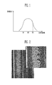
- FIG. 1 is a graph showing energy distribution of laser
- FIG. 2 is an enlarged photograph showing a bonding state of a sealing material and a substrate with an incomplete bonding at side portions;
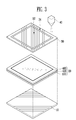
- FIG. 3 is an exploded perspective view for explaining a sealing device according to the present invention.
- FIGs. 4a and 4b are plan views for explaining a mask according to the first embodiment of the present invention.
- FIG. 4c is a plan view for explaining a mask according to the second embodiment of the present invention.
- FIG. 4d is a plan view for explaining a mask according to the third embodiment of the present invention.
- FIGs. 5a, 5b, and 5d are plan views for explaining a method of manufacturing an organic light emitting display device using a sealing device according to the present invention
- FIGs. 5c and 5e are cross-sectional views for explaining a method of manufacturing an organic light emitting display device using a sealing device according to the present invention.
- FIG. 6 is a cross-sectional view for explaining the organic light emitting display device of FIG. 5a.
- FIG. 3 is an exploded perspective view for explaining a sealing device according to an embodiment of the present invention.
- the sealing device includes a stage 10 to which a display panel 20 is mounted, a mask 30 disposed on one side of the display panel 20 opposed to the stage 10, in which a transmission portion 34 is formed at a portion corresponding to a sealing material 420, and an optical head 40 irradiating light to the sealing material 420 along the transmission portion 34.
- the optical head 40 can be moved by a drive means along the transmission portion 34 and irradiates the light such as laser provided from a light source through a lens so as to have a predetermined width.
- a display panel 20 can include a support substrate 100 in which an organic light emitting device is formed, an encapsulation substrate 400 disposed opposite to the support substrate 100, and a sealing material 420 interposed between the support substrate 100 and the encapsulation substrate 400 for sealing the organic light emitting device.
- the mask 30 includes an organic substrate or a transparent substrate such as quartz and a pattern formed of chrome, etc. on the transparent substrate.
- the transmission portion 34 is formed at a portion corresponding to the sealing material 420 of the display panel 20 by a chrome pattern 32.
- the chrome pattern 32 is formed at a portion corresponding to the organic light emitting device to interrupt the light and the light can be transmitted through the transmission portion 34 in which the chrome pattern 32 is not formed.
- chrome patterns 36a to 36g for regulating the amount of the transmitted light are formed in the transmission portion 34 of the mask 30.
- the transmission portion 34 includes a plurality of regions in which the densities of the formed patterns are different.
- density of a pattern is used to indicate the percentage of a unit area that is covered by the pattern.
- the transmission portion 34 is divided into a first region 34a at a central portion, a second region 34b including the first region 34a and wider than the first region 34a, and a third region 34c including the second region 34b and wider than the second region 34b.
- Line-shaped patterns 36a to 36c crossing each other can be formed in the first to third regions 34a to 34c, respectively.
- the line-shaped pattern can be formed parallel to each other and equidistant from each other. Then, as shown in FIG.
- the densities of the patterns become lower as they go in the order of the first region 34a, the second region 34b, and the third region 34c by the arrangement of the patterns 36a to 36c, i.e. the light transmittance increases as the density of the patterns descreases.
- the densities of the patterns of the second region 34b and/or third regions 34c on the inner side are higher than the densities of the patterns of the second region 34b and/or third regions 34c on the outer side, with reference to the first region 34a of the central portion. If the densities of the patterns 36a to 36c of the first to third regions 34a to 34c are regulated, the amounts of light transmitted to the first to third regions 34a to 34c can be regulated, respectively.
- the transmission portion 34 is divided into a first region 34d on the inner side and a second region 34e on the outer side.
- the densities of the patterns 36d and 36e of the first region 34d and the second region 34e can be formed differently.
- the line-shaped patterns can be formed in the first region 34d and the second region 34e, respectively. Then, if the densities of the patterns 36d and 36e of the first region 34d are set to be higher than the second region 34e by crossing the patterns 36d and 36e in the first region 34d, the light transmittance in the first region 34d becomes lower than the light transmittance in the second region 34e.
- the transmission portion 34 is divided into a first region 34f at a central portion and a second region 34g on both sides of the first region 34f.
- the densities of the patterns 36f and 36g of the first region 34f and the second region 34g can be formed differently.
- line-shaped patterns 36f and 36g can be formed in the first region 34f and the second region 34g, respectively. Then, if the densities of the patterns 36f and 36g of the first region 34f are set to be higher than the second region 34g by crossing the patterns 36f and 36g in the first region 34f, the light transmittance in the first region 34f becomes lower than the light transmittance in the second region 34g.
- the shape, the density, the line width, and the interval of the patterns 36a to 36g can be selected according to the kind of light used and to its energy distribution.
- the patterns 36a to 36g are formed in the entire regions of the transmission portion 34 has been explained, they can be selectively formed in some regions of the transmission portion 34.
- a pattern may not be formed in a peripheral region in which the laser energy is low and can be formed a central portion in which the laser energy is high.
- a substrate 100 defining a pixel region 110 and a non-pixel region 120 is prepared.
- a plurality of organic light emitting devices 200 connected between a scan line 104 and a data line 106 in the form of matrix are formed in the substrate 100 of the pixel region 110.
- a scan line 104 and a data line 106 extending from the scan line 104 and the data line 106 in the pixel region 110, a power source supply line (not shown) for the operation of the organic light emitting devices 200, and a scan drive section 310 and a data drive section 320 processing a signal provided from outside through a pad 108 and supplying the signal to the scan line 104 and the data line 106 are formed in the substrate 100 of the non-pixel region 120.
- the organic light emitting display 200 includes an anode electrode 208 and a cathode electrode 211, and an organic thin film layer 210 formed between the anode electrode 208 and the cathode electrode 211.
- the organic thin film layer 210 has a structure in which a hole transportation layer, an organic light emitting layer, and an electron transportation layer are stacked and can further include a hole implantation layer and an electron implantation layer. Further, the organic thin film layer can further include a capacitor for maintaining a switching transistor and a signal for controlling the operation of the organic light emitting device 200.
- a buffer layer 201 is formed on the substrate 100 of the pixel region 110 and the non-pixel region 120.
- the buffer 201 prevents damage to the substrate 100 due to heat and diffusion of ions from the substrate 100 to the outside, and is formed of an insulation layer such as a silicon dioxide layer (SiO 2 ) or a silicon nitride layer (SiNx).
- a gate insulation layer 203 is formed on the upper surface of the pixel region 110 including the semiconductor layer 202.
- a gate electrode 204 is formed on the gate insulation layer 203 at an upper portion of the semiconductor layer 202. Then, the scan line 104 connected to the gate electrode 204 is formed in the pixel region 110, and a scan line 104 extending from the scan line 104 of the pixel region 110 and a pad 108 for receiving a signal from outside are formed in the non-pixel region 120.
- the gate electrode 204, the scan line 104, and the pad 108 can be formed of a metal such as molybdenum (Mo), tungsten (W), titanium (Ti), and aluminum (Al) or an alloy of the metals, or by stacking the metals.
- An interlayer insulation layer 205 is formed on the entire upper surface of the pixel region 110 including the gate electrode 204.
- a contact hole is formed by patterning the interlayer insulation layer 205 and the gate insulation layer 203 so that the source and drain regions of the semiconductor layer 202 can be exposed and source and drain electrodes 206a and 206b are formed through the contact hole so as to source and drain regions. Then, a data line 106 connected to the source and drain electrodes 206a and 206b is formed in the pixel region 110 and the data line 106 extending from the data line 106 of the pixel region and the pad for providing a signal from outside are formed in the non-pixel region.
- the source and drain electrodes 206a and 206b, the data line 106, and the pad 108 can be formed of a metal such as molybdenum (Mo), tungsten (W), titanium (Ti), and aluminum (Al) or an alloy of the metals, or by stacking the metals.
- Mo molybdenum
- W tungsten
- Ti titanium
- Al aluminum
- a planarization layer 207 is formed on the entire upper surface of the pixel region and the surface is planarized.
- a via hole is formed by patterning the planarization layer 207 so that a predetermined portion of the source or drain electrode 206a or 206b and the anode electrode connected to the source or drain electrode 206 or 206b is formed through the via hole.
- an organic thin film layer 210 is formed on the exposed anode electrode 208 and a cathode electrode 211 is formed on the entire upper surface including the organic thin film layer 210.
- an encapsulation substrate 400 for encapsulating the pixel region 110 is prepared and a sealing material 420 is formed along the peripheral portion of the encapsulation substrate 400.
- the encapsulation substrate 400 can use a substrate formed of a transparent material such as glass and the sealing material 420 can use a frit including an organic binder and a filler for reducing the thermal expansion coefficient.
- a paste frit can be coated along a peripheral portion of the encapsulation substrate 400 and be plasticized to remove moisture and the organic binder.
- the organic light emitting device 200 is sealed by the sealing material 420.
- the substrate 100 and the encapsulation substrate 400 disposed opposite to each other, with the sealing material 420 being interposed therebetween, are mounted to the stage of the sealing device and the mask is located at an upper thereof.
- the mask 30 is mounted at the position at which the sealing material 420 is formed so that the transmission portion 34 can correspond to the sealing material 420.
- the sealing material 420 is melted by the laser energy so that the substrate 100 can be bonded to the encapsulation substrate 400, thereby uniformizing the amount of the irradiated laser by the patterns 36a to 36g formed in the transmission portion 34 of the mask 30.
- the amount of the laser irradiated to the sealing material at the portion corresponding to a laser central portion D2 having high energy is significantly reduced by the patterns 36a to 36c formed in the first region 34a of the transmission portion 34
- the amount of the laser irradiated to the sealing material 420 at the portions corresponding to the laser both side portions D1 and D3 having relatively low energy is only slightly decreased by the patterns 36b and 36c formed in the second and third regions 34b and 34c
- the amount of laser radiation transmitted through the mask is more uniform than the laser beam so that the sealing material 420 can be uniformly bonded to the substrate 100.
- the laser is moving at a faster speed in an inner side of the curved portion than in an outer side. Since the densities of the patterns 36a to 36c formed in the first region 34a and the second and third regions 34b and 34c on the inner side of the first region 34a are higher than the densities of the patterns 36b and 36c formed in the second and third regions 34b and 34c on the outer side of the first region 34a, the amount of the irradiated laser in the inner region is decreased more than in the outer region, thereby uniformizing the interface bonding. (Refer to FIG. 4b)
- the amount of the irradiated laser is uniformized on the whole according to the densities of the patterns 36d to 36g, thereby uniformizing the bonding on the whole.
- the present invention is not limited thereto and the encapsulated portion can include the scan drive section 310. In this case, the size of the encapsulation substrate 400 also should be changed. Further, although the cases in which the sealing material 420 is formed on the encapsulation substrate 400 have been described, the present invention is not limited thereto and the sealing material 420 can be formed on the substrate 100. Furthermore, although a laser is used to bond the sealing material to the substrate 100, another light source such as infrared ray can be used.
- the present invention forms patterns for regulating the amount of light irradiated to a transmission portion of a mask.
- a sealing material and a substrate can be uniformly bonded to each other with uniform energy distribution by selectively decreasing the amount of irradiated light at a portion having high energy and a portion having a slow movement speed. Therefore, the bonding force of the sealing material and the substrate can be reinforced so that penetration of hydrogen, oxygen, or moisture can be perfectly prevented, thereby improving the sealing effect and the reliability and effectively preventing damage to a display device due to an impact.
Landscapes
- Engineering & Computer Science (AREA)
- Manufacturing & Machinery (AREA)
- Physics & Mathematics (AREA)
- Plasma & Fusion (AREA)
- Thermal Sciences (AREA)
- Electroluminescent Light Sources (AREA)
- Devices For Indicating Variable Information By Combining Individual Elements (AREA)
- Liquid Crystal (AREA)
Abstract
Description
- This application claims the benefit of
Korean Patent Application No. 2006-0110572, filed November 9, 2006 - The present invention relates to a sealing device and a method of manufacturing a display device using the sealing device, and more particularly to a sealing device including a mask for partially irradiating light and a method of manufacturing a display device using the sealing device.
- Generally, an organic light display device includes a substrate provided a pixel region and a non-pixel region, and a container or a substrate disposed opposite to the substrate for encapsulation and adhered to the substrate by a sealant such as epoxy.
- A plurality of light emitting devices connected between a scan line and a date line in the form of matrix are formed in the pixel region of the substrate, and the light emitting device includes an anode electrode and a cathode electrode, and an organic thin film layer formed between the anode electrode and the cathode electrode and having a hole transportation layer, an organic light emitting layer, and an electron transportation layer.
- However, the light emitting device is vulnerable to hydrogen and oxygen since it contains an organic material and is easily oxidized by moisture in air so that the electrical and light emitting characteristic thereof are deteriorated since the cathode electrode is formed of a metal material. In order to prevent this problem, moisture penetrating from outside is removed by mounting a moisture absorbing material to a container in the form of a can or a cup of a metal material or a substrate of glass or plastic in the form of powder or by bonding the container or the substrate in the form of a film.
- However, the method of mounting the moisture absorbing material in the form of powder complicates the process and increases the material and process costs, thereby increasing the thickness of the display device. So, it is difficult to apply the method to entire surface light emission. Further, the method of bonding a moisture absorbing material in the form of a film can limitedly remove moisture and has low durability and reliability, thereby making mass-production difficult.
- In order to solve the above-mentioned problem, a method using a sealing material such as a frit and bonding the sealing material by irradiating laser has been used.
-
Korean Patent Laid-Open No. 2001-0084380 (September 6, 2001 -
Korean Patent Laid-Open No. 2002-0051153 (June 28, 2002 - In the case in which a sealing material is bonded to a substrate by irradiating laser, since the energy of the laser has a Gaussian distribution as shown in FIG. 1, the differences between the energies between a central portion D2 and both side portions D1 and D3 make the bonding between the sealing material and the substrate weaker. FIG. 2 is an enlarged plan view photographed after laser is irradiated to the sealing material. In FIG. 2, the bonding state of the sealing material and the substrate is represented by the differences of lightness and shading. More particularly, a central portion in which the sealing material and the substrate are properly bonded by sufficient energy is bright, and both side portions in which the sealing material and the substrate are incompletely bonded by relatively low energy are dark. Further, even at a corner portion on which a sealing material is coated in a curved way, since laser is irradiated less at an inner side portion than at an outer side portion due to the difference of the moving speeds of laser, the bonding of the outer side portion is weaker. Therefore, if an impact is applied to a portion in which the interface bonding state of the sealing material and the substrate, the sealing material is easily separated, thereby harming the sealing state.
- Accordingly, certain inventive aspects provide a sealing device capable of uniformly bonding a sealing material and a substrate.
- One inventive aspect is a method of manufacturing a display device using a sealing device capable of improving the sealing effect and the reliability by uniformly bonding a sealing material and a substrate.
- One aspect of the invention is a sealing device for bonding a first substrate and a second substrate by interposing a sealing material along edges of the first substrate and the second substrate and by irradiating light to the sealing material.
- The sealing device comprises: a mask, disposed on the second substrate stacked on the first substrate, comprising a transmission portion formed in correspondence to the sealing material; and an optical head irradiating the light to the sealing material through the transmission portion of the mask. The transmission portion of the mask comprises a plurality of patterns for regulating the light irradiated to the sealing material.
- The transmission portion of the mask can comprise a plurality of regions having patterns with different transmittances. The plurality of patterns can be aligned with at least of a part of the sealing material. The energy distribution of the light across the sealing material can be controlled by the plurality of patterns.
- The transmission portion can comprise a first region at a central portion thereof and a second region on both sides of the first region, and the transmittances of the patterns in the first region and the second region can be different. The transmittance of the pattern in the first region can be lower than that of the second region. The pattern can comprise a plurality of opaque lines, and the transmittance can be controlled by density of the opaque lines of the patterns. Preferably, the opaque lines are arranged parallel to each other and equidistant from each other.
- The transmission portion can comprise a first region on an inner side of a curved corner potion and a second region on an outer side of the curved corner portion and the transmittances of the patterns of the first region and the second region are different. The transmittance of the pattern in the first region can be lower than that of the second region.
- The transmission portion can comprise a first region at a central portion, a second region provided on both sides of the first region, and a third region provided on both outer sides of the second region, and the transmittances of the patterns of the first region, the second region, and the third region can be different. The first, second, and third regions can comprise line-shaped patterns comprising a plurality of opaque lines, and the transmittance can be controlled by density of the opaque lines of the patterns.
- The light can comprise one of laser and infrared ray.
- The device can further comprise a stage on which the first and second substrates interposing the sealing material in between are mounted.
- Other aspect of the invention provides a method of manufacturing a display device having first and second substrates and a sealing material. The method comprises: irradiating light through a mask located on the second substrate; regulating the energy profile of the light irradiated across the sealing material interposed between the first and second substrates using the mask; and bonding the sealing material to the first substrate and the second substrate.
- The regulating the energy profile of the light can comprise passing the light through a mask having a transmission portion. The transmission portion can comprise a plurality of regions having pattern with different transmittances.
- The transmission portion can comprise a first region at a central portion thereof and a second region on both sides of the first region, and wherein the transmittances of the patterns in the first region and the second region are different. The density of the pattern in the first region can be lower than that of the second region.
According to another aspect of the present invention, the transmission portion may a first region on an inner side of a curved corner portion and a second region on an outer side of the curved corner portion and the transmittances of the patterns of the first region and the second region may be different. Preferably, the density of the pattern in the first region is lower than that of the pattern in the second region.
Preferably, each of the plurality of patterns comprises a plurality of opaque lines, and the transmittance is controlled by density of the opaque lines of the patterns.
The light may comprise laser and infrared ray. Preferably, the display device comprises an organic light emitting display device. - The method can further comprise, prior to irradiating: mounting a first substrate and a second substrate to a stage by disposing the first substrate and the second substrate so as to be opposite to each other, with a sealing material being located between the first substrate and the second substrate; and locating the mask in which a transmission portion is formed at a plurality of portions corresponding to the formed sealing material and a plurality of patterns are formed at the transmission portion.
According to another aspect, a sealing device used to bond a first substrate and a second substrate by interposing a sealing material at edges of the first substrate and the second substrate opposite to each other and by irradiating light to the sealing material comprises: a stage to which the first substrate and the second substrate between which the sealing material is interposed is mounted; a mask disposed on one side of the stage, in which a transmission portion is formed in correspondence to the formation position of the sealing member so that light can be irradiated to the sealing material; and an optical head irradiating the light to the sealing material through the transmission portion of the mask. In the sealing device, a pattern for regulating the amount of the light irradiated to the sealing material is formed in the transmission portion of the mask.
According to another aspect of the present invention, a method of manufacturing a display device comprises the steps of: mounting a first substrate and a second substrate to a stage by disposing the first substrate and the second substrate so as to be opposite to each other, with a sealing material being located between the first substrate and the second substrate; locating a mask in which a transmission portion is formed at a portion corresponding to the position of the formed sealing material and a predetermined pattern is formed at the transmission portion; and bonding the sealing material to the first substrate by irradiating light to the transmission portion. In the method, the amount of the irradiated light is regulated by the pattern formed in the transmission portion. - These and/or other aspects and advantages of the invention will become apparent and more readily appreciated from the following description of the embodiments, taken in conjunction with the accompanying drawings of which:
- FIG. 1 is a graph showing energy distribution of laser;
- FIG. 2 is an enlarged photograph showing a bonding state of a sealing material and a substrate with an incomplete bonding at side portions;
- FIG. 3 is an exploded perspective view for explaining a sealing device according to the present invention;
- FIGs. 4a and 4b are plan views for explaining a mask according to the first embodiment of the present invention;
- FIG. 4c is a plan view for explaining a mask according to the second embodiment of the present invention;
- FIG. 4d is a plan view for explaining a mask according to the third embodiment of the present invention;
- FIGs. 5a, 5b, and 5d are plan views for explaining a method of manufacturing an organic light emitting display device using a sealing device according to the present invention;
- FIGs. 5c and 5e are cross-sectional views for explaining a method of manufacturing an organic light emitting display device using a sealing device according to the present invention; and
- FIG. 6 is a cross-sectional view for explaining the organic light emitting display device of FIG. 5a.
- Hereinafter, embodiments according to the present invention will be described with reference to the accompanying drawings. The embodiments are provided to allow those skilled in the art to sufficiently understand the present invention and can be varied in various forms. Further, the scope of the present invention is not limited to the embodiments.
- FIG. 3 is an exploded perspective view for explaining a sealing device according to an embodiment of the present invention. The sealing device includes a
stage 10 to which adisplay panel 20 is mounted, amask 30 disposed on one side of thedisplay panel 20 opposed to thestage 10, in which atransmission portion 34 is formed at a portion corresponding to a sealingmaterial 420, and anoptical head 40 irradiating light to the sealingmaterial 420 along thetransmission portion 34. Theoptical head 40 can be moved by a drive means along thetransmission portion 34 and irradiates the light such as laser provided from a light source through a lens so as to have a predetermined width. - A
display panel 20 can include asupport substrate 100 in which an organic light emitting device is formed, anencapsulation substrate 400 disposed opposite to thesupport substrate 100, and a sealingmaterial 420 interposed between thesupport substrate 100 and theencapsulation substrate 400 for sealing the organic light emitting device. - The
mask 30 includes an organic substrate or a transparent substrate such as quartz and a pattern formed of chrome, etc. on the transparent substrate. Thetransmission portion 34 is formed at a portion corresponding to the sealingmaterial 420 of thedisplay panel 20 by achrome pattern 32. In other words, thechrome pattern 32 is formed at a portion corresponding to the organic light emitting device to interrupt the light and the light can be transmitted through thetransmission portion 34 in which thechrome pattern 32 is not formed. - In addition, as shown in FIGs. 4a to 4d,
chrome patterns 36a to 36g for regulating the amount of the transmitted light are formed in thetransmission portion 34 of themask 30. - According to the first embodiment of the present invention, the
transmission portion 34 includes a plurality of regions in which the densities of the formed patterns are different. Hereinafter, the term density of a pattern is used to indicate the percentage of a unit area that is covered by the pattern. For example, thetransmission portion 34 is divided into afirst region 34a at a central portion, asecond region 34b including thefirst region 34a and wider than thefirst region 34a, and athird region 34c including thesecond region 34b and wider than thesecond region 34b. Line-shapedpatterns 36a to 36c crossing each other can be formed in the first tothird regions 34a to 34c, respectively. The line-shaped pattern can be formed parallel to each other and equidistant from each other. Then, as shown in FIG. 4a, in a portion in which thetransmission portion 34 is linearly formed, the densities of the patterns become lower as they go in the order of thefirst region 34a, thesecond region 34b, and thethird region 34c by the arrangement of thepatterns 36a to 36c, i.e. the light transmittance increases as the density of the patterns descreases. Further, as shown in FIG. 4b, in a curved corner portion of the transmission portion, the densities of the patterns of thesecond region 34b and/orthird regions 34c on the inner side are higher than the densities of the patterns of thesecond region 34b and/orthird regions 34c on the outer side, with reference to thefirst region 34a of the central portion. If the densities of thepatterns 36a to 36c of the first tothird regions 34a to 34c are regulated, the amounts of light transmitted to the first tothird regions 34a to 34c can be regulated, respectively. - According to the second embodiment of the present invention, as shown in FIG. 4c, the
transmission portion 34 is divided into afirst region 34d on the inner side and asecond region 34e on the outer side. The densities of thepatterns first region 34d and thesecond region 34e can be formed differently. For example, the line-shaped patterns can be formed in thefirst region 34d and thesecond region 34e, respectively. Then, if the densities of thepatterns first region 34d are set to be higher than thesecond region 34e by crossing thepatterns first region 34d, the light transmittance in thefirst region 34d becomes lower than the light transmittance in thesecond region 34e. - According to the third embodiment, as shown in FIG. 4d, the
transmission portion 34 is divided into afirst region 34f at a central portion and asecond region 34g on both sides of thefirst region 34f. The densities of thepatterns first region 34f and thesecond region 34g can be formed differently. For example, line-shapedpatterns first region 34f and thesecond region 34g, respectively. Then, if the densities of thepatterns first region 34f are set to be higher than thesecond region 34g by crossing thepatterns first region 34f, the light transmittance in thefirst region 34f becomes lower than the light transmittance in thesecond region 34g. - In the embodiments, the shape, the density, the line width, and the interval of the
patterns 36a to 36g can be selected according to the kind of light used and to its energy distribution. In addition, in the embodiments, although the case in which thepatterns 36a to 36g are formed in the entire regions of thetransmission portion 34 has been explained, they can be selectively formed in some regions of thetransmission portion 34. For example, a pattern may not be formed in a peripheral region in which the laser energy is low and can be formed a central portion in which the laser energy is high. - Hereinafter, a method of manufacturing an organic light emitting device using the sealing device according to the present invention will be described with reference to FIG. 5a to 5e.
- Referring to FIG. 5a, a
substrate 100 defining apixel region 110 and anon-pixel region 120 is prepared. A plurality of organiclight emitting devices 200 connected between ascan line 104 and adata line 106 in the form of matrix are formed in thesubstrate 100 of thepixel region 110. Ascan line 104 and adata line 106 extending from thescan line 104 and thedata line 106 in thepixel region 110, a power source supply line (not shown) for the operation of the organiclight emitting devices 200, and ascan drive section 310 and adata drive section 320 processing a signal provided from outside through apad 108 and supplying the signal to thescan line 104 and thedata line 106 are formed in thesubstrate 100 of thenon-pixel region 120. - Referring to FIG. 6, the organic
light emitting display 200 according to an embodiment of the present invention includes ananode electrode 208 and acathode electrode 211, and an organicthin film layer 210 formed between theanode electrode 208 and thecathode electrode 211. The organicthin film layer 210 has a structure in which a hole transportation layer, an organic light emitting layer, and an electron transportation layer are stacked and can further include a hole implantation layer and an electron implantation layer. Further, the organic thin film layer can further include a capacitor for maintaining a switching transistor and a signal for controlling the operation of the organiclight emitting device 200. - Hereinafter, the manufacturing process of the organic
light emitting device 200 will be described in more detail with reference to FIG. 6. - First, a
buffer layer 201 is formed on thesubstrate 100 of thepixel region 110 and thenon-pixel region 120. Thebuffer 201 prevents damage to thesubstrate 100 due to heat and diffusion of ions from thesubstrate 100 to the outside, and is formed of an insulation layer such as a silicon dioxide layer (SiO2) or a silicon nitride layer (SiNx). - After a
semiconductor layer 202 providing a source/drain region and a channel region is formed on thebuffer layer 201 of thepixel region 110, agate insulation layer 203 is formed on the upper surface of thepixel region 110 including thesemiconductor layer 202. - A gate electrode 204 is formed on the
gate insulation layer 203 at an upper portion of thesemiconductor layer 202. Then, thescan line 104 connected to the gate electrode 204 is formed in thepixel region 110, and ascan line 104 extending from thescan line 104 of thepixel region 110 and apad 108 for receiving a signal from outside are formed in thenon-pixel region 120. The gate electrode 204, thescan line 104, and thepad 108 can be formed of a metal such as molybdenum (Mo), tungsten (W), titanium (Ti), and aluminum (Al) or an alloy of the metals, or by stacking the metals. - An
interlayer insulation layer 205 is formed on the entire upper surface of thepixel region 110 including the gate electrode 204. A contact hole is formed by patterning theinterlayer insulation layer 205 and thegate insulation layer 203 so that the source and drain regions of thesemiconductor layer 202 can be exposed and source and drain electrodes 206a and 206b are formed through the contact hole so as to source and drain regions. Then, adata line 106 connected to the source and drain electrodes 206a and 206b is formed in thepixel region 110 and thedata line 106 extending from thedata line 106 of the pixel region and the pad for providing a signal from outside are formed in the non-pixel region. The source and drain electrodes 206a and 206b, thedata line 106, and thepad 108 can be formed of a metal such as molybdenum (Mo), tungsten (W), titanium (Ti), and aluminum (Al) or an alloy of the metals, or by stacking the metals. - A
planarization layer 207 is formed on the entire upper surface of the pixel region and the surface is planarized. A via hole is formed by patterning theplanarization layer 207 so that a predetermined portion of the source or drain electrode 206a or 206b and the anode electrode connected to the source or drain electrode 206 or 206b is formed through the via hole. - After a
pixel defining layer 209 is formed on theplanarization layer 207 so that a portion of theanode electrode 208 can be exposed, an organicthin film layer 210 is formed on the exposedanode electrode 208 and acathode electrode 211 is formed on the entire upper surface including the organicthin film layer 210. - Referring to FIGs. 5b and 5c, an
encapsulation substrate 400 for encapsulating thepixel region 110 is prepared and a sealingmaterial 420 is formed along the peripheral portion of theencapsulation substrate 400. Theencapsulation substrate 400 can use a substrate formed of a transparent material such as glass and the sealingmaterial 420 can use a frit including an organic binder and a filler for reducing the thermal expansion coefficient. For example, a paste frit can be coated along a peripheral portion of theencapsulation substrate 400 and be plasticized to remove moisture and the organic binder. - As shown in FIGs. 5d and 5e, after the
encapsulation substrate 400 is disposed at an upper portion of thesubstrate 100 opposite to thesubstrate 100, the organiclight emitting device 200 is sealed by the sealingmaterial 420. - The
substrate 100 and theencapsulation substrate 400 disposed opposite to each other, with the sealingmaterial 420 being interposed therebetween, are mounted to the stage of the sealing device and the mask is located at an upper thereof. Themask 30 is mounted at the position at which the sealingmaterial 420 is formed so that thetransmission portion 34 can correspond to the sealingmaterial 420. - Next, if the laser is irradiated to the sealing
material 420 through thetransmission portion 34 while theoptical head 40 is moving along thetransmission portion 34 of themask 30, the sealingmaterial 420 is melted by the laser energy so that thesubstrate 100 can be bonded to theencapsulation substrate 400, thereby uniformizing the amount of the irradiated laser by thepatterns 36a to 36g formed in thetransmission portion 34 of themask 30. - In other words, since the amount of the laser irradiated to the sealing material at the portion corresponding to a laser central portion D2 having high energy is significantly reduced by the
patterns 36a to 36c formed in thefirst region 34a of thetransmission portion 34, while the amount of the laser irradiated to the sealingmaterial 420 at the portions corresponding to the laser both side portions D1 and D3 having relatively low energy is only slightly decreased by thepatterns third regions material 420 can be uniformly bonded to thesubstrate 100. - In addition, at curved corner portions of the sealing
material 420, the laser is moving at a faster speed in an inner side of the curved portion than in an outer side. Since the densities of thepatterns 36a to 36c formed in thefirst region 34a and the second andthird regions first region 34a are higher than the densities of thepatterns third regions first region 34a, the amount of the irradiated laser in the inner region is decreased more than in the outer region, thereby uniformizing the interface bonding. (Refer to FIG. 4b) - Similarly, even in the case of the embodiments of FIGs. 4c and 4d, the amount of the irradiated laser is uniformized on the whole according to the densities of the
patterns 36d to 36g, thereby uniformizing the bonding on the whole. - On the other hand, although the cases in which the sealing
material 420 seals thepixel region 110 have been described in the embodiments, the present invention is not limited thereto and the encapsulated portion can include thescan drive section 310. In this case, the size of theencapsulation substrate 400 also should be changed. Further, although the cases in which the sealingmaterial 420 is formed on theencapsulation substrate 400 have been described, the present invention is not limited thereto and the sealingmaterial 420 can be formed on thesubstrate 100. Furthermore, although a laser is used to bond the sealing material to thesubstrate 100, another light source such as infrared ray can be used. - As mentioned above, the present invention forms patterns for regulating the amount of light irradiated to a transmission portion of a mask. A sealing material and a substrate can be uniformly bonded to each other with uniform energy distribution by selectively decreasing the amount of irradiated light at a portion having high energy and a portion having a slow movement speed. Therefore, the bonding force of the sealing material and the substrate can be reinforced so that penetration of hydrogen, oxygen, or moisture can be perfectly prevented, thereby improving the sealing effect and the reliability and effectively preventing damage to a display device due to an impact.
- As mentioned above, certain inventive embodiments have been disclosed through the detailed description and the accompanying drawings. The terms have been used not to restrict the scope of the present invention described in the claims but just to explain the present invention. Accordingly, those skilled in the art can understand that various modifications and other embodiments equivalent to the embodiments of the present invention are possible. Therefore, the true technical protection scope of the present invention should be determined by the following claims.
Claims (20)
- A sealing device for bonding a first substrate (100) and a second substrate (400) by interposing a sealing material (420) along edges of the first substrate (100) and the second substrate (400) and by irradiating light on the sealing material (420), the sealing device comprising:a mask (30), disposed on the second substrate (400) stacked on the first substrate (100), comprising a transmission portion (34) formed in correspondence to the sealing material (420); andan optical head (40) for irradiating light to the sealing material (420) through the transmission portion (34) of the mask (30),wherein the transmission portion (34) of the mask (30) comprises a plurality of patterns (36a, 36b, 36c, 36d, 36e, 36f, 36g) adapted for regulating the intensity of the light irradiated to the sealing material (420).
- The sealing device of claim 1, wherein the transmission portion (34) of the mask (30) comprises a plurality of regions (34a, 34b, 34c, 34d, 34e, 34f, 34g) having patterns (36a, 36b, 36c, 36d, 36e, 36f, 36g) with different transmittances for controlling the intensity distribution of the light irradiated to the sealing material (420).
- The sealing device of one of the preceding claims, wherein each of the plurality of patterns (36a, 36b, 36c, 36d, 36e, 36f, 36g) comprises a plurality of opaque lines, and wherein the transmittance is controlled by density of the opaque lines of the patterns (36a, 36b, 36c, 36d, 36e, 36f, 36g).
- The sealing device of one of the preceding claims, wherein the transmission portion (34) comprises a first region (34a, 34f) at a central portion thereof and a second region (34b, 34g) on both sides of the first region (34a, 34f), and wherein the transmittances of the patterns (36a, 36b, 36f, 36g) in the first region (34a, 34f) and the second region (34b, 34g) are different.
- The sealing device of one of claims 1-3, wherein the transmission portion (34) comprises a first region (34d) on an inner side of a curved corner portion and a second region (34e) on an outer side of the curved corner portion and the transmittances of the patterns (36d, 36e) of the first region (34d) and the second region (34e) are different.
- The sealing device of claim 4, wherein the transmission portion (34) further comprises a third region (34c) provided on both outer sides of the second region (34b), and wherein the transmittances of the patterns (36a, 36b, 36c) of the first region (34a), the second region (34b), and the third region (34c) are different.
- The sealing device of one of claims 4-6, wherein the transmittance of the pattern in the first region (34a, 34f, 34d) is lower than that of the second region (34f, 34g, 34e)
- The sealing device of one of the preceding claims, wherein the light comprises one of laser and infrared ray.
- The sealing device of one of the preceding claims, further comprising a stage (10) on which the first and second substrates (100, 400) interposing the sealing material (420) in between are mounted.
- A method of manufacturing a display device having first and second substrates (100, 400) and a sealing material (420), the method comprising:irradiating light through a mask (30) disposed on the second substrate (400);regulating the energy profile of the light irradiated to the sealing material (420) interposed between the first and second substrates (100, 400) using the mask (30); andbonding the sealing material (420) to the first substrate (100) and the second substrate (400).
- The method of claim 10, wherein the mask (30) has a transmission portion (34).
- The method of claim 11, wherein the transmission portion (34) comprises a plurality of regions (34a, 34b, 34c, 34d, 34e, 34f, 34g) having patterns (36a, 36b, 36c, 36d, 36e, 36f, 36g) with different transmittances.
- The method of one of claims 11-12, wherein the transmission portion (34) comprises a first region (34a, 34f) at a central portion thereof and a second region (34b, 34g) on both sides of the first region (34a, 34f), and wherein the transmittances of the patterns (36a, 36b, 36f, 36g) in the first region (34a, 34f) and the second region (34b, 34g) are different.
- The method of claim 13, wherein the transmission portion (34) further comprises a third region (34c) provided on both outer sides of the second region (34b), and wherein the transmittances of the patterns (36a, 36b, 36c) of the first region (34a), the second region (34b), and the third region (34c) are different.
- The method of one of claims 11-12, wherein the transmission portion (34) comprises a first region (34d) on an inner side of a curved corner portion and a second region (34e) on an outer side of the curved corner portion and the transmittances of the patterns (36d, 36e) of the first region (34d) and the second region (34e) are different.
- The method of one of claims 13-15, wherein the transmittance of the pattern (36a, 36d, 36f) in the first region (34a, 34d, 34f) is lower than that of the pattern (36b, 36e, 36g) in the second region (34b, 34e, 34g).
- The method of one of claims 10-16, wherein each of the plurality of patterns (36a, 36b, 36c, 36d, 36e, 36f, 36g) comprise a plurality of opaque lines, and wherein the transmittance is controlled by density of the opaque lines of the patterns.
- The method of one of claims 10-17, wherein the light comprises laser and infrared ray.
- The method of one of claims 10-18, wherein the display device comprises an organic light emitting display device.
- The method of one of claims 10-19, further comprising, prior to irradiating:mounting a first substrate (100) and a second substrate (400) to a stage (10) by disposing the first substrate (100) and the second substrate (400) so as to be opposite to each other, with a sealing material (420) being located between the first substrate (100) and the second substrate (400); andlocating the mask (30) in which a transmission portion (34) is formed at a plurality of portions corresponding to the sealing material (420) and a plurality of patterns (36a, 36b, 36c, 36d, 36e, 36f, 36g) are formed at the transmission portion (34).
Applications Claiming Priority (1)
| Application Number | Priority Date | Filing Date | Title |
|---|---|---|---|
| KR1020060110572A KR100846975B1 (en) | 2006-11-09 | 2006-11-09 | Sealing device and manufacturing method of display device using same |
Publications (3)
| Publication Number | Publication Date |
|---|---|
| EP1921651A2 true EP1921651A2 (en) | 2008-05-14 |
| EP1921651A3 EP1921651A3 (en) | 2008-07-30 |
| EP1921651B1 EP1921651B1 (en) | 2010-03-03 |
Family
ID=39146887
Family Applications (1)
| Application Number | Title | Priority Date | Filing Date |
|---|---|---|---|
| EP07120244A Active EP1921651B1 (en) | 2006-11-09 | 2007-11-08 | Sealing device and method of manufacturing display device using the same |
Country Status (7)
| Country | Link |
|---|---|
| US (2) | US8371353B2 (en) |
| EP (1) | EP1921651B1 (en) |
| JP (1) | JP4659724B2 (en) |
| KR (1) | KR100846975B1 (en) |
| CN (1) | CN101179032B (en) |
| DE (1) | DE602007005078D1 (en) |
| TW (1) | TWI361017B (en) |
Families Citing this family (23)
| Publication number | Priority date | Publication date | Assignee | Title |
|---|---|---|---|---|
| JP2009123421A (en) * | 2007-11-13 | 2009-06-04 | Canon Inc | Airtight container manufacturing method |
| US8448468B2 (en) * | 2008-06-11 | 2013-05-28 | Corning Incorporated | Mask and method for sealing a glass envelope |
| WO2011010489A1 (en) * | 2009-07-23 | 2011-01-27 | 旭硝子株式会社 | Method and apparatus for manufacturing glass member provided with sealing material layer and method for manufacturing electronic device |
| KR101084231B1 (en) * | 2009-10-05 | 2011-11-16 | 삼성모바일디스플레이주식회사 | Laser irradiation system and laser irradiation method |
| KR101135538B1 (en) * | 2009-11-16 | 2012-04-13 | 삼성모바일디스플레이주식회사 | Display device and method for menufacturing display device |
| KR101084175B1 (en) | 2009-11-23 | 2011-11-17 | 삼성모바일디스플레이주식회사 | Organic light emitting display device and manufacturing method thereof |
| KR101084179B1 (en) * | 2009-12-28 | 2011-11-17 | 삼성모바일디스플레이주식회사 | Sealing method of organic light emitting display device |
| JP5590935B2 (en) * | 2010-03-29 | 2014-09-17 | キヤノン株式会社 | Airtight container manufacturing method |
| JP2011210430A (en) * | 2010-03-29 | 2011-10-20 | Canon Inc | Method for manufacturing hermetic container |
| JP2011210431A (en) * | 2010-03-29 | 2011-10-20 | Canon Inc | Method for manufacturing hermetic container |
| KR101137394B1 (en) * | 2010-07-05 | 2012-04-20 | 삼성모바일디스플레이주식회사 | Laser beam irradiation apparatus and substrate sealing apparatus comprising the same |
| JP2012059401A (en) | 2010-09-06 | 2012-03-22 | Canon Inc | Method for manufacturing airtight container |
| JP5627370B2 (en) | 2010-09-27 | 2014-11-19 | キヤノン株式会社 | Depressurized airtight container and image display device manufacturing method |
| KR20120044020A (en) * | 2010-10-27 | 2012-05-07 | 삼성모바일디스플레이주식회사 | Organic light emitting display apparatus and method of manufacturing thereof |
| KR101693347B1 (en) | 2010-12-03 | 2017-01-06 | 삼성디스플레이 주식회사 | Display apparatus and method of manufacturing display apparatus |
| JP5737011B2 (en) * | 2011-01-18 | 2015-06-17 | 日本電気硝子株式会社 | LIGHT EMITTING DEVICE, LIGHT EMITTING DEVICE CELL, AND LIGHT EMITTING DEVICE MANUFACTURING METHOD |
| TWI569490B (en) * | 2011-11-28 | 2017-02-01 | 半導體能源研究所股份有限公司 | Sealing body, light emitting module, and method of manufacturing the same |
| WO2013115627A1 (en) | 2012-02-03 | 2013-08-08 | 주식회사 엘지화학 | Adhesive film |
| TWI505525B (en) * | 2013-01-18 | 2015-10-21 | Innolux Corp | Display apparatus and the sealing method thereof |
| JP5705937B2 (en) * | 2013-09-13 | 2015-04-22 | 信越エンジニアリング株式会社 | Bonding device manufacturing apparatus and manufacturing method |
| CN103552354B (en) * | 2013-10-29 | 2016-08-17 | 深圳市联得自动化装备股份有限公司 | Applying method and equipment |
| JP6175644B2 (en) * | 2014-08-19 | 2017-08-09 | 株式会社Joled | Display device and electronic device |
| KR20220000440A (en) * | 2020-06-25 | 2022-01-04 | 삼성디스플레이 주식회사 | Display device and method of fabricating the same |
Citations (4)
| Publication number | Priority date | Publication date | Assignee | Title |
|---|---|---|---|---|
| KR20010084380A (en) | 2000-02-25 | 2001-09-06 | 김순택 | Method for sealing a glass flat display panel with a frit frame using a laser |
| KR20020051153A (en) | 2000-12-22 | 2002-06-28 | 김순택 | Method for laser vacuum packaging of flat-panel display |
| JP2004185827A (en) | 2002-11-29 | 2004-07-02 | Nippon Seiki Co Ltd | Ultraviolet ray cutting mask and sealing device |
| US20060082298A1 (en) | 2004-10-20 | 2006-04-20 | Becken Keith J | Optimization of parameters for sealing organic emitting light diode (OLED) displays |
Family Cites Families (19)
| Publication number | Priority date | Publication date | Assignee | Title |
|---|---|---|---|---|
| JP2773661B2 (en) * | 1994-11-28 | 1998-07-09 | 日本電気株式会社 | Beam scanning type laser marking method and apparatus and mask therefor |
| US5840147A (en) | 1995-06-07 | 1998-11-24 | Edison Welding Institute | Plastic joining method |
| US5690775A (en) * | 1996-03-07 | 1997-11-25 | Westvaco Corporation | Apparatus for heat sealing paperboard substrates using a uniform energy distributed light energy beam |
| JP3237544B2 (en) | 1996-10-11 | 2001-12-10 | 富士通株式会社 | Manufacturing method of flat display panel and flat display panel |
| RU2000111546A (en) | 1997-10-01 | 2002-08-10 | Комплит Дисплей Солушнз Лимитед (Gb) | PICTURE INDICATOR |
| US6290589B1 (en) | 1998-12-09 | 2001-09-18 | Applied Materials, Inc. | Polishing pad with a partial adhesive coating |
| ES2149637T3 (en) | 1999-01-28 | 2000-11-01 | Leister Process Tech | LASER ASSEMBLY PROCEDURE AND DEVICE TO JOIN DIFFERENT PLASTIC OR PLASTIC PIECES WITH OTHER MATERIALS. |
| TW493358B (en) | 2001-06-14 | 2002-07-01 | Ritdisplay Corp | Package method and apparatus of organic light-emitting diode display device |
| US6569706B2 (en) | 2001-09-19 | 2003-05-27 | Osram Opto Semiconductors Gmbh | Fabrication of organic light emitting diode using selective printing of conducting polymer layers |
| JP2003177506A (en) * | 2001-12-13 | 2003-06-27 | Sony Corp | Photolithography mask, thin film forming method, liquid crystal display device, and method of manufacturing liquid crystal display device |
| EP2009676B8 (en) | 2002-05-08 | 2012-11-21 | Phoseon Technology, Inc. | A semiconductor materials inspection system |
| KR100858802B1 (en) * | 2002-07-31 | 2008-09-17 | 삼성에스디아이 주식회사 | Manufacturing Method of Electroluminescent Device |
| KR100675625B1 (en) | 2002-08-08 | 2007-02-01 | 엘지.필립스 엘시디 주식회사 | Organic electroluminescent device and manufacturing method thereof |
| US7255770B2 (en) | 2002-08-12 | 2007-08-14 | Mentor Corporation | Method for laser welding flexible polymers |
| JP4267378B2 (en) * | 2003-06-11 | 2009-05-27 | トヨタ自動車株式会社 | Laser welding method and apparatus for resin member, and laser welding member |
| TWI248773B (en) | 2004-04-09 | 2006-02-01 | Grace Semiconductor Mfg Corp | Structure and encapsulation method of organic electro-luminance light-emitting display device |
| KR100640952B1 (en) * | 2004-12-29 | 2006-11-02 | 동부일렉트로닉스 주식회사 | Metal wiring formation method of semiconductor device |
| FR2881591A1 (en) | 2005-02-03 | 2006-08-04 | France Telecom | Cryptographic operation e.g. digital certificate request, implementing method, involves performing cryptographic operation on data provided by user, and recording information associated to operation |
| DE202006008749U1 (en) | 2006-03-23 | 2006-08-03 | Hella Kgaa Hueck & Co. | Device for heating the seams when welding thermoplastic parts, e.g. parts of car headlights, comprises tubular radiation sources covering the seam and a focussing mask with internal reflective surfaces |
-
2006
- 2006-11-09 KR KR1020060110572A patent/KR100846975B1/en not_active Expired - Fee Related
- 2006-12-01 JP JP2006325767A patent/JP4659724B2/en not_active Expired - Fee Related
-
2007
- 2007-03-16 US US11/724,854 patent/US8371353B2/en active Active
- 2007-09-13 TW TW096134238A patent/TWI361017B/en not_active IP Right Cessation
- 2007-10-10 CN CN2007101809780A patent/CN101179032B/en active Active
- 2007-11-08 EP EP07120244A patent/EP1921651B1/en active Active
- 2007-11-08 DE DE602007005078T patent/DE602007005078D1/en active Active
-
2013
- 2013-02-11 US US13/764,519 patent/US8512503B2/en not_active Expired - Fee Related
Patent Citations (4)
| Publication number | Priority date | Publication date | Assignee | Title |
|---|---|---|---|---|
| KR20010084380A (en) | 2000-02-25 | 2001-09-06 | 김순택 | Method for sealing a glass flat display panel with a frit frame using a laser |
| KR20020051153A (en) | 2000-12-22 | 2002-06-28 | 김순택 | Method for laser vacuum packaging of flat-panel display |
| JP2004185827A (en) | 2002-11-29 | 2004-07-02 | Nippon Seiki Co Ltd | Ultraviolet ray cutting mask and sealing device |
| US20060082298A1 (en) | 2004-10-20 | 2006-04-20 | Becken Keith J | Optimization of parameters for sealing organic emitting light diode (OLED) displays |
Also Published As
| Publication number | Publication date |
|---|---|
| DE602007005078D1 (en) | 2010-04-15 |
| US8371353B2 (en) | 2013-02-12 |
| US20080110561A1 (en) | 2008-05-15 |
| KR100846975B1 (en) | 2008-07-17 |
| JP4659724B2 (en) | 2011-03-30 |
| EP1921651A3 (en) | 2008-07-30 |
| CN101179032A (en) | 2008-05-14 |
| TW200822791A (en) | 2008-05-16 |
| TWI361017B (en) | 2012-03-21 |
| US20130153141A1 (en) | 2013-06-20 |
| JP2008123977A (en) | 2008-05-29 |
| EP1921651B1 (en) | 2010-03-03 |
| US8512503B2 (en) | 2013-08-20 |
| CN101179032B (en) | 2011-10-26 |
| KR20080042321A (en) | 2008-05-15 |
Similar Documents
| Publication | Publication Date | Title |
|---|---|---|
| EP1921651B1 (en) | Sealing device and method of manufacturing display device using the same | |
| JP4633674B2 (en) | Organic electroluminescent display device and manufacturing method thereof | |
| EP1814177B1 (en) | Oganic light-emitting display device and method for fabricating the same | |
| KR100671647B1 (en) | Organic light emitting display device | |
| KR100671638B1 (en) | Organic electroluminescent display | |
| KR100688796B1 (en) | Organic light emitting display device and manufacturing method thereof | |
| EP1814174B1 (en) | Organic light-emitting display device and method for fabricating the same | |
| CN100448062C (en) | Organic electroluminescent display and method of fabricating the same | |
| KR100671643B1 (en) | Organic light emitting display device and manufacturing method thereof | |
| KR100703472B1 (en) | Frit curing device and curing method using the same | |
| US7846001B2 (en) | Manufacture and method of sealing an organic light emitting display | |
| EP1814175B1 (en) | Organic light emitting display device and a method of manufacturing thereof | |
| CN101009312A (en) | Organic light emitting display device and manufacturing therefor | |
| TWI538273B (en) | Electrical device and method of manufacturing same | |
| KR100754120B1 (en) | Manufacturing method of organic light emitting display device | |
| KR100671645B1 (en) | Fabrication method of organic light emitting display device | |
| KR20080015629A (en) | Organic light emitting display device |
Legal Events
| Date | Code | Title | Description |
|---|---|---|---|
| PUAI | Public reference made under article 153(3) epc to a published international application that has entered the european phase |
Free format text: ORIGINAL CODE: 0009012 |
|
| 17P | Request for examination filed |
Effective date: 20071108 |
|
| AK | Designated contracting states |
Kind code of ref document: A2 Designated state(s): AT BE BG CH CY CZ DE DK EE ES FI FR GB GR HU IE IS IT LI LT LU LV MC MT NL PL PT RO SE SI SK TR |
|
| AX | Request for extension of the european patent |
Extension state: AL BA HR MK RS |
|
| PUAL | Search report despatched |
Free format text: ORIGINAL CODE: 0009013 |
|
| AK | Designated contracting states |
Kind code of ref document: A3 Designated state(s): AT BE BG CH CY CZ DE DK EE ES FI FR GB GR HU IE IS IT LI LT LU LV MC MT NL PL PT RO SE SI SK TR |
|
| AX | Request for extension of the european patent |
Extension state: AL BA HR MK RS |
|
| RIC1 | Information provided on ipc code assigned before grant |
Ipc: H01J 17/18 20060101AFI20080313BHEP Ipc: B29C 65/14 20060101ALI20080620BHEP Ipc: H01J 9/26 20060101ALI20080620BHEP |
|
| RAP1 | Party data changed (applicant data changed or rights of an application transferred) |
Owner name: SAMSUNG MOBILE DISPLAY CO., LTD. |
|
| AKX | Designation fees paid |
Designated state(s): DE FR GB HU |
|
| 17Q | First examination report despatched |
Effective date: 20090512 |
|
| GRAP | Despatch of communication of intention to grant a patent |
Free format text: ORIGINAL CODE: EPIDOSNIGR1 |
|
| RIC1 | Information provided on ipc code assigned before grant |
Ipc: H01L 51/52 20060101ALI20091002BHEP Ipc: H01J 9/26 20060101ALI20091002BHEP Ipc: H01J 5/24 20060101ALI20091002BHEP Ipc: H01J 17/18 20060101AFI20091002BHEP |
|
| GRAS | Grant fee paid |
Free format text: ORIGINAL CODE: EPIDOSNIGR3 |
|
| GRAA | (expected) grant |
Free format text: ORIGINAL CODE: 0009210 |
|
| AK | Designated contracting states |
Kind code of ref document: B1 Designated state(s): DE FR GB HU |
|
| REG | Reference to a national code |
Ref country code: GB Ref legal event code: FG4D |
|
| REF | Corresponds to: |
Ref document number: 602007005078 Country of ref document: DE Date of ref document: 20100415 Kind code of ref document: P |
|
| REG | Reference to a national code |
Ref country code: DE Ref legal event code: R096 Ref document number: 602007005078 Country of ref document: DE Effective date: 20100415 |
|
| PLBE | No opposition filed within time limit |
Free format text: ORIGINAL CODE: 0009261 |
|
| STAA | Information on the status of an ep patent application or granted ep patent |
Free format text: STATUS: NO OPPOSITION FILED WITHIN TIME LIMIT |
|
| 26N | No opposition filed |
Effective date: 20101206 |
|
| REG | Reference to a national code |
Ref country code: DE Ref legal event code: R097 Ref document number: 602007005078 Country of ref document: DE Effective date: 20101206 |
|
| PG25 | Lapsed in a contracting state [announced via postgrant information from national office to epo] |
Ref country code: HU Free format text: LAPSE BECAUSE OF FAILURE TO SUBMIT A TRANSLATION OF THE DESCRIPTION OR TO PAY THE FEE WITHIN THE PRESCRIBED TIME-LIMIT Effective date: 20100904 |
|
| REG | Reference to a national code |
Ref country code: GB Ref legal event code: 732E Free format text: REGISTERED BETWEEN 20130103 AND 20130109 |
|
| REG | Reference to a national code |
Ref country code: DE Ref legal event code: R082 Ref document number: 602007005078 Country of ref document: DE Representative=s name: GULDE HENGELHAUPT ZIEBIG & SCHNEIDER, DE |
|
| REG | Reference to a national code |
Ref country code: DE Ref legal event code: R082 Ref document number: 602007005078 Country of ref document: DE Representative=s name: GULDE HENGELHAUPT ZIEBIG & SCHNEIDER, DE Effective date: 20130416 Ref country code: DE Ref legal event code: R081 Ref document number: 602007005078 Country of ref document: DE Owner name: SAMSUNG DISPLAY CO., LTD., KR Free format text: FORMER OWNER: SAMSUNG MOBILE DISPLAY CO. LTD., SUWON, KR Effective date: 20130416 Ref country code: DE Ref legal event code: R081 Ref document number: 602007005078 Country of ref document: DE Owner name: SAMSUNG DISPLAY CO., LTD., YONGIN-CITY, KR Free format text: FORMER OWNER: SAMSUNG MOBILE DISPLAY CO. LTD., SUWON, GYEONGGI, KR Effective date: 20130416 Ref country code: DE Ref legal event code: R082 Ref document number: 602007005078 Country of ref document: DE Representative=s name: GULDE & PARTNER PATENT- UND RECHTSANWALTSKANZL, DE Effective date: 20130416 |
|
| REG | Reference to a national code |
Ref country code: FR Ref legal event code: PLFP Year of fee payment: 9 |
|
| REG | Reference to a national code |
Ref country code: FR Ref legal event code: PLFP Year of fee payment: 10 |
|
| REG | Reference to a national code |
Ref country code: FR Ref legal event code: PLFP Year of fee payment: 11 |
|
| REG | Reference to a national code |
Ref country code: FR Ref legal event code: PLFP Year of fee payment: 12 |
|
| P01 | Opt-out of the competence of the unified patent court (upc) registered |
Effective date: 20230515 |
|
| PGFP | Annual fee paid to national office [announced via postgrant information from national office to epo] |
Ref country code: DE Payment date: 20241021 Year of fee payment: 18 |
|
| PGFP | Annual fee paid to national office [announced via postgrant information from national office to epo] |
Ref country code: GB Payment date: 20241021 Year of fee payment: 18 |
|
| PGFP | Annual fee paid to national office [announced via postgrant information from national office to epo] |
Ref country code: FR Payment date: 20241022 Year of fee payment: 18 |