EP1921082A1 - Silanylamine-based compound, method of preparing the same and organic light emitting device including organic layer comprising the silanylamine-based compound - Google Patents
Silanylamine-based compound, method of preparing the same and organic light emitting device including organic layer comprising the silanylamine-based compound Download PDFInfo
- Publication number
- EP1921082A1 EP1921082A1 EP07119446A EP07119446A EP1921082A1 EP 1921082 A1 EP1921082 A1 EP 1921082A1 EP 07119446 A EP07119446 A EP 07119446A EP 07119446 A EP07119446 A EP 07119446A EP 1921082 A1 EP1921082 A1 EP 1921082A1
- Authority
- EP
- European Patent Office
- Prior art keywords
- groups
- substituted
- unsubstituted
- group
- compound
- Prior art date
- Legal status (The legal status is an assumption and is not a legal conclusion. Google has not performed a legal analysis and makes no representation as to the accuracy of the status listed.)
- Granted
Links
- 0 C*(C=Cc1c(C)c(cc(C)cc2)c2[n]1-c1ccccc1)=C Chemical compound C*(C=Cc1c(C)c(cc(C)cc2)c2[n]1-c1ccccc1)=C 0.000 description 5
- UFGFGDSWSWQBAL-UHFFFAOYSA-N Cc(cc1)cc(c2cc(C)ccc22)c1[n]2-c(cc1)ccc1C#N Chemical compound Cc(cc1)cc(c2cc(C)ccc22)c1[n]2-c(cc1)ccc1C#N UFGFGDSWSWQBAL-UHFFFAOYSA-N 0.000 description 1
- CBSIVTQLZPVCDT-UHFFFAOYSA-N Cc(cc1)cc(c2cc(C)ccc22)c1[n]2-c(cc1)ccc1F Chemical compound Cc(cc1)cc(c2cc(C)ccc22)c1[n]2-c(cc1)ccc1F CBSIVTQLZPVCDT-UHFFFAOYSA-N 0.000 description 1
- XIPVJZXRVSTQQN-UHFFFAOYSA-N Cc(cc1)ccc1N(C(CC1)=CC=C1N(c1ccccc1)C1=CCCC=C1)c(cc1c2cc([Si+](c3ccccc3)(c3ccccc3)c3ccccc3)ccc22)ccc1[n]2-c1ccccc1 Chemical compound Cc(cc1)ccc1N(C(CC1)=CC=C1N(c1ccccc1)C1=CCCC=C1)c(cc1c2cc([Si+](c3ccccc3)(c3ccccc3)c3ccccc3)ccc22)ccc1[n]2-c1ccccc1 XIPVJZXRVSTQQN-UHFFFAOYSA-N 0.000 description 1
- CWHHLKXRFCIKCN-UHFFFAOYSA-N Cc(cc1)ccc1N(c(cc1)ccc1-c1ccccc1)c(cc1c2c3ccc([Si+](c4ccccc4)(c4ccccc4)c4ccccc4)c2)ccc1[n]3-c1ccccc1 Chemical compound Cc(cc1)ccc1N(c(cc1)ccc1-c1ccccc1)c(cc1c2c3ccc([Si+](c4ccccc4)(c4ccccc4)c4ccccc4)c2)ccc1[n]3-c1ccccc1 CWHHLKXRFCIKCN-UHFFFAOYSA-N 0.000 description 1
- RUGBNLDVLUFQML-UHFFFAOYSA-N Cc(cc1)ccc1N(c(cc1)ccc1Oc1ccccc1)C(C=CC12)=CC1c(cc(cc1)[Si+](c3ccccc3)(c3ccccc3)c3ccccc3)c1N2c1ccccc1 Chemical compound Cc(cc1)ccc1N(c(cc1)ccc1Oc1ccccc1)C(C=CC12)=CC1c(cc(cc1)[Si+](c3ccccc3)(c3ccccc3)c3ccccc3)c1N2c1ccccc1 RUGBNLDVLUFQML-UHFFFAOYSA-N 0.000 description 1
- LUTKLDZQNPCRHA-UHFFFAOYSA-N Cc(cc1)ccc1N(c(cc1c2c3ccc([Si+](c4ccccc4)(c4ccccc4)c4ccccc4)c2)ccc1[n]3-c1ccccc1)c1c(cccc2)c2ccc1 Chemical compound Cc(cc1)ccc1N(c(cc1c2c3ccc([Si+](c4ccccc4)(c4ccccc4)c4ccccc4)c2)ccc1[n]3-c1ccccc1)c1c(cccc2)c2ccc1 LUTKLDZQNPCRHA-UHFFFAOYSA-N 0.000 description 1
- YXDDQRGQQAIWQL-UHFFFAOYSA-N Cc(cc1)ccc1N(c(cc1c2c3ccc([Si+](c4ccccc4)(c4ccccc4)c4ccccc4)c2)ccc1[n]3-c1ccccc1)c1cc2ccccc2cc1 Chemical compound Cc(cc1)ccc1N(c(cc1c2c3ccc([Si+](c4ccccc4)(c4ccccc4)c4ccccc4)c2)ccc1[n]3-c1ccccc1)c1cc2ccccc2cc1 YXDDQRGQQAIWQL-UHFFFAOYSA-N 0.000 description 1
- QWVPVODXKGOBLF-UHFFFAOYSA-N Fc(cc1)ccc1-[n](c(cccc1)c1c1c2)c1ccc2N(c(cc1)ccc1Oc1ccccc1)c(cc1c2cc([Si](c3ccccc3)(c3ccccc3)c3ccccc3)ccc22)ccc1[n]2-c(cc1)ccc1F Chemical compound Fc(cc1)ccc1-[n](c(cccc1)c1c1c2)c1ccc2N(c(cc1)ccc1Oc1ccccc1)c(cc1c2cc([Si](c3ccccc3)(c3ccccc3)c3ccccc3)ccc22)ccc1[n]2-c(cc1)ccc1F QWVPVODXKGOBLF-UHFFFAOYSA-N 0.000 description 1
- ARJYRMJRKGYGAF-UHFFFAOYSA-N Fc(cc1)ccc1-[n](c1ccccc1c1c2)c1ccc2N(c(cc1)ccc1-c1ccccc1)c(cc1c2c3ccc([Si+](c4ccccc4)(c4ccccc4)c4ccccc4)c2)ccc1[n]3-c(cc1)ccc1F Chemical compound Fc(cc1)ccc1-[n](c1ccccc1c1c2)c1ccc2N(c(cc1)ccc1-c1ccccc1)c(cc1c2c3ccc([Si+](c4ccccc4)(c4ccccc4)c4ccccc4)c2)ccc1[n]3-c(cc1)ccc1F ARJYRMJRKGYGAF-UHFFFAOYSA-N 0.000 description 1
- FOSBIOMVMPCSMZ-UHFFFAOYSA-N Fc(cc1)ccc1-[n](c1ccccc1c1c2)c1ccc2N(c(cc1c2c3ccc([Si+](c4ccccc4)(c4ccccc4)c4ccccc4)c2)ccc1[n]3-c(cc1)ccc1F)c1cc(cccc2)c2cc1 Chemical compound Fc(cc1)ccc1-[n](c1ccccc1c1c2)c1ccc2N(c(cc1c2c3ccc([Si+](c4ccccc4)(c4ccccc4)c4ccccc4)c2)ccc1[n]3-c(cc1)ccc1F)c1cc(cccc2)c2cc1 FOSBIOMVMPCSMZ-UHFFFAOYSA-N 0.000 description 1
- QWZXJHAIHFPCTL-UHFFFAOYSA-N Fc(cc1)ccc1-[n]1c(ccc(N(c(cc2)ccc2-c(cc2)ccc2[Si+](c2ccccc2)(c2ccccc2)c2ccccc2)c(cc2)ccc2Oc2ccccc2)c2)c2c2ccccc12 Chemical compound Fc(cc1)ccc1-[n]1c(ccc(N(c(cc2)ccc2-c(cc2)ccc2[Si+](c2ccccc2)(c2ccccc2)c2ccccc2)c(cc2)ccc2Oc2ccccc2)c2)c2c2ccccc12 QWZXJHAIHFPCTL-UHFFFAOYSA-N 0.000 description 1
- HOFFHMSQYKEZMV-UHFFFAOYSA-N Fc(cc1)ccc1-[n]1c(ccc(N(c(cc2)ccc2-c(cc2)ccc2[SiH-](c2ccccc2)(c2ccccc2)c2ccccc2)c(cc2)ccc2N(c2ccccc2)c2ccccc2)c2)c2c2ccccc12 Chemical compound Fc(cc1)ccc1-[n]1c(ccc(N(c(cc2)ccc2-c(cc2)ccc2[SiH-](c2ccccc2)(c2ccccc2)c2ccccc2)c(cc2)ccc2N(c2ccccc2)c2ccccc2)c2)c2c2ccccc12 HOFFHMSQYKEZMV-UHFFFAOYSA-N 0.000 description 1
- BGYXFGZGKSTGSM-UHFFFAOYSA-N Fc(cc1)ccc1N(C1C=CC(F)=CC1)c(cc1c2c3ccc([Si](c4ccccc4)(c4ccccc4)c4ccccc4)c2)ccc1[n]3-c1ccccc1 Chemical compound Fc(cc1)ccc1N(C1C=CC(F)=CC1)c(cc1c2c3ccc([Si](c4ccccc4)(c4ccccc4)c4ccccc4)c2)ccc1[n]3-c1ccccc1 BGYXFGZGKSTGSM-UHFFFAOYSA-N 0.000 description 1
- YNLQSZYNKVCAKD-UHFFFAOYSA-N Fc(cc1)ccc1N(C1C=CC=C2C=CC=CC12)c(cc1c2c3ccc([Si+](c4ccccc4)(c4ccccc4)c4ccccc4)c2)ccc1[n]3-c1ccccc1 Chemical compound Fc(cc1)ccc1N(C1C=CC=C2C=CC=CC12)c(cc1c2c3ccc([Si+](c4ccccc4)(c4ccccc4)c4ccccc4)c2)ccc1[n]3-c1ccccc1 YNLQSZYNKVCAKD-UHFFFAOYSA-N 0.000 description 1
- LCAUDSOSVXLGFF-UHFFFAOYSA-N Fc(cc1)ccc1N(c(cc1)ccc1-c1ccccc1)c(cc1c2c3ccc([Si+](c4ccccc4)(c4ccccc4)c4ccccc4)c2)ccc1[n]3-c1ccccc1 Chemical compound Fc(cc1)ccc1N(c(cc1)ccc1-c1ccccc1)c(cc1c2c3ccc([Si+](c4ccccc4)(c4ccccc4)c4ccccc4)c2)ccc1[n]3-c1ccccc1 LCAUDSOSVXLGFF-UHFFFAOYSA-N 0.000 description 1
- FPSKOXZBWMPXAR-UHFFFAOYSA-N Fc(cc1)ccc1N(c(cc1)ccc1Oc1ccccc1)c(cc1c2c3ccc([Si+](c4ccccc4)(c4ccccc4)C4=CCCC=C4)c2)ccc1[n]3-c1ccccc1 Chemical compound Fc(cc1)ccc1N(c(cc1)ccc1Oc1ccccc1)c(cc1c2c3ccc([Si+](c4ccccc4)(c4ccccc4)C4=CCCC=C4)c2)ccc1[n]3-c1ccccc1 FPSKOXZBWMPXAR-UHFFFAOYSA-N 0.000 description 1
- IEDQMJCTWYHTKT-UHFFFAOYSA-N Fc(cc1)ccc1N(c(cc1c2cc([Si+](c3ccccc3)(c3ccccc3)c3ccccc3)ccc22)ccc1[n]2-c1ccccc1)c1cc(cccc2)c2cc1 Chemical compound Fc(cc1)ccc1N(c(cc1c2cc([Si+](c3ccccc3)(c3ccccc3)c3ccccc3)ccc22)ccc1[n]2-c1ccccc1)c1cc(cccc2)c2cc1 IEDQMJCTWYHTKT-UHFFFAOYSA-N 0.000 description 1
- WWHRPRLWPSGVJD-UHFFFAOYSA-N N#Cc(cc1)ccc1N(c(cc1)ccc1F)c(cc1c2c3ccc([Si+](c4ccccc4)(c4ccccc4)c4ccccc4)c2)ccc1[n]3-c1ccccc1 Chemical compound N#Cc(cc1)ccc1N(c(cc1)ccc1F)c(cc1c2c3ccc([Si+](c4ccccc4)(c4ccccc4)c4ccccc4)c2)ccc1[n]3-c1ccccc1 WWHRPRLWPSGVJD-UHFFFAOYSA-N 0.000 description 1
Images

Classifications
-
- C—CHEMISTRY; METALLURGY
- C07—ORGANIC CHEMISTRY
- C07F—ACYCLIC, CARBOCYCLIC OR HETEROCYCLIC COMPOUNDS CONTAINING ELEMENTS OTHER THAN CARBON, HYDROGEN, HALOGEN, OXYGEN, NITROGEN, SULFUR, SELENIUM OR TELLURIUM
- C07F7/00—Compounds containing elements of Groups 4 or 14 of the Periodic Table
- C07F7/02—Silicon compounds
- C07F7/08—Compounds having one or more C—Si linkages
- C07F7/0803—Compounds with Si-C or Si-Si linkages
- C07F7/081—Compounds with Si-C or Si-Si linkages comprising at least one atom selected from the elements N, O, halogen, S, Se or Te
- C07F7/0812—Compounds with Si-C or Si-Si linkages comprising at least one atom selected from the elements N, O, halogen, S, Se or Te comprising a heterocyclic ring
- C07F7/0814—Compounds with Si-C or Si-Si linkages comprising at least one atom selected from the elements N, O, halogen, S, Se or Te comprising a heterocyclic ring said ring is substituted at a C ring atom by Si
-
- C—CHEMISTRY; METALLURGY
- C07—ORGANIC CHEMISTRY
- C07F—ACYCLIC, CARBOCYCLIC OR HETEROCYCLIC COMPOUNDS CONTAINING ELEMENTS OTHER THAN CARBON, HYDROGEN, HALOGEN, OXYGEN, NITROGEN, SULFUR, SELENIUM OR TELLURIUM
- C07F7/00—Compounds containing elements of Groups 4 or 14 of the Periodic Table
- C07F7/02—Silicon compounds
- C07F7/08—Compounds having one or more C—Si linkages
- C07F7/10—Compounds having one or more C—Si linkages containing nitrogen having a Si-N linkage
-
- C—CHEMISTRY; METALLURGY
- C07—ORGANIC CHEMISTRY
- C07F—ACYCLIC, CARBOCYCLIC OR HETEROCYCLIC COMPOUNDS CONTAINING ELEMENTS OTHER THAN CARBON, HYDROGEN, HALOGEN, OXYGEN, NITROGEN, SULFUR, SELENIUM OR TELLURIUM
- C07F7/00—Compounds containing elements of Groups 4 or 14 of the Periodic Table
- C07F7/02—Silicon compounds
- C07F7/08—Compounds having one or more C—Si linkages
-
- C—CHEMISTRY; METALLURGY
- C07—ORGANIC CHEMISTRY
- C07F—ACYCLIC, CARBOCYCLIC OR HETEROCYCLIC COMPOUNDS CONTAINING ELEMENTS OTHER THAN CARBON, HYDROGEN, HALOGEN, OXYGEN, NITROGEN, SULFUR, SELENIUM OR TELLURIUM
- C07F7/00—Compounds containing elements of Groups 4 or 14 of the Periodic Table
- C07F7/02—Silicon compounds
- C07F7/08—Compounds having one or more C—Si linkages
- C07F7/0803—Compounds with Si-C or Si-Si linkages
- C07F7/081—Compounds with Si-C or Si-Si linkages comprising at least one atom selected from the elements N, O, halogen, S, Se or Te
-
- Y—GENERAL TAGGING OF NEW TECHNOLOGICAL DEVELOPMENTS; GENERAL TAGGING OF CROSS-SECTIONAL TECHNOLOGIES SPANNING OVER SEVERAL SECTIONS OF THE IPC; TECHNICAL SUBJECTS COVERED BY FORMER USPC CROSS-REFERENCE ART COLLECTIONS [XRACs] AND DIGESTS
- Y10—TECHNICAL SUBJECTS COVERED BY FORMER USPC
- Y10S—TECHNICAL SUBJECTS COVERED BY FORMER USPC CROSS-REFERENCE ART COLLECTIONS [XRACs] AND DIGESTS
- Y10S428/00—Stock material or miscellaneous articles
- Y10S428/917—Electroluminescent
Definitions
- the present invention relates to silanylamine-based compounds, methods of preparing the same, and organic light emitting devices including organic layers comprising a silanylamine-based compound.
- OLEDs Organic light emitting devices
- OLEDs are self-emitting devices having wide viewing angles, excellent contrast, and quick responses.
- Organic light emitting devices have low operating voltages and quick response times, and can realize multi-color images. Accordingly, OLEDs are being extensively researched.
- a typical organic light emitting device has an anode/emissive layer/cathode structure.
- Organic light emitting devices can also have various other structures, such as anode/hole transport layer/emissive layer/cathode, and anode/hole transport layer/emissive layer/electron injection layer/cathode.
- These alternative structures are realized by further including an electron transport layer and at least one of a hole injection layer, a hole transport layer and an electron injection layer between the anode and the emissive layer, or between the emissive layer and the cathode.
- Fluorene and anthracene derivatives have been used as to form the hole transport layer.
- organic light emitting devices having these hole transport layers do not have satisfactory lifetime, efficiency, and power consumption.
- a silanylamine-based compound represented by Formula I below is provided.
- X is selected from the group consisting of substituted or unsubstituted C 1 -C 30 alkylene groups, substituted or unsubstituted C 6 -C 30 arylene groups, substituted or unsubstituted C 2 -C 30 heteroarylene groups;
- n is an integer ranging from 0 to 5;
- Ar 1 and Ar 2 are each independently selected from the group consisting of hydrogen, substituted or unsubstituted C 6 -C 30 aryl groups, substituted or unsubstituted C 2 -C 30 heteroaryl groups;
- R 1 , R 2 and R 3 are each independently selected from the group consisting of hydrogen, substituted or unsubstituted C 1 -C 30 alkyl groups, substituted or unsubstituted C 2 -C 30 alkenyl groups, substituted or unsubstituted C 2 -C 30 alkynyl groups,
- a method of preparing a silanylamine-based compound represented by Formula I includes reacting a compound represented by Formula 1a and a compound represented by Formula 1 b via Reaction Scheme 1 below.
- X, n, Ar 1 , Ar 2 , R 1 , R 2 and R 3 are as described above, and Y isa halogen atom.
- an organic light emitting device includes a first electrode, a second electrode, and an organic layer positioned between the first electrode and the second electrode, the organic layer including the silanylamine-based compound of formula I.
- the organic light emitting device including the silanylamine-based compound represented by Formula I exhibits low driving voltage, excellent luminance, high efficiency, high current density and has a long lifetime.
- FIG. 1 is a schematic illustrating an organic light emitting device according to one embodiment of the present invention
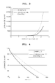
- FIG. 2 is a graph of luminance according to driving voltage of organic light emitting devices prepared according to Example 1 and Comparative Example 1;
- FIG. 3 is a graph of luminance according to driving voltage of organic light emitting devices prepared according to Example 2 and Comparative Example 1;
- FIG. 4 is a graph of luminance according to time of organic light emitting devices prepared according to Example 3 and Comparative Example 1.
- a silanylamine-based compound is represented by Formula I below.
- an amine derivative is bonded to a silane derivative through a linking group -(X) n - to form the silanylamine-based compound.
- n may be an integer ranging from 0 to 5, preferably from 1 to 5, and X may be selected from substituted and unsubstituted C 1 -C 30 alkylene groups, substituted and unsubstituted C 6 -C 30 arylene groups, and substituted and unsubstituted C 2 -C 30 heteroarylene groups.
- Ar 1 and Ar 2 may be each independently selected from hydrogen atoms, substituted and unsubstituted C 6 -C 30 aryl groups, and substituted and unsubstituted C 2 -C 30 heteroaryl groups.
- R 1 , R 2 and R 3 may be each independently selected from hydrogen atoms, substituted and unsubstituted C 1 -C 30 alkyl groups, substituted and unsubstituted C 2 -C 30 alkenyl groups, substituted and unsubstituted C 2 -C 30 alkynyl groups, substituted and unsubstituted C 1 -C 30 alkoxy groups, substituted and unsubstituted C 6 -C 30 aryloxy groups, substituted and unsubstituted C 6 -C 30 aryl groups, and substituted and unsubstituted C 2 -C 30 heteroaryl groups. At least two of R 1 , R 2 and R 3 may be bonded to each other to form a saturated or unsaturated ring.
- Suitable unsubstituted C 1 -C 30 alkyl groups of R 1 to R 3 include methyl, ethyl, propyl, isobutyl, sec-butyl, pentyl, iso-amyl, and hexyl.
- At least one of the hydrogen atoms in the mentioned alkyl groups may be substituted with a constituent selected from halogen, hydroxy, nitro, cyano, amino groups, amidino groups, hydrazines, hydrazones, carboxyl and salts thereof, sulfonic acid and salts thereof, phosphoric acid and salts thereof, C 1 -C 30 alkenyl groups, C 1 -C 30 alkynyl groups, C 6 -C 30 aryl groups, C 7 -C 20 arylalkyl groups, C 2 -C 20 heteroaryl groups, C 3 -C 30 heteroarylalkyl groups, C 6 -C 30 aryloxy groups and -N(Z 1 )(Z 2 ).
- Z 1 and Z 2 may be each independently selected from hydrogen, substituted and unsubstituted C 1 -C 30 alkyl groups, substituted and unsubstituted C 1 -C 30 haloalkyl groups, substituted and unsubstituted C 6 -C 30 aryl groups, substituted and unsubstituted C 6 -C 30 haloaryl groups, and substituted and unsubstituted C 2 -C 30 heteroaryl groups.
- the unsubstituted C 1 -C 30 alkylene group of the linking group X is a bivalent linking group having a structure similar to an alkyl group, and preferred examples of the alkylene group include methylene groups and ethylene groups. At least one hydrogen atom in the alkylene group may be substituted with any of the substituents described above in connection with the unsubstituted C 1 -C 30 alkyl group.
- Preferred examples of the unsubstituted C 1 -C 30 alkoxy group of R 1 to R 3 include methoxy groups, ethoxy groups, phenyloxy groups, cyclohexyloxy groups, naphthyloxy groups, isopropyloxy groups, and diphenyloxy groups. At least one of the hydrogen atoms in the alkoxy group may be substituted with any of the substituents described above in connection with the unsubstituted C 1 -C 30 alkyl group.
- the C 2 -C 30 alkenyl group of the linking group X is a hydrocarbon chain having a carbon-carbon double bond in the center or at one end of the alkyl group structure.
- suitable alkenyl groups include ethylene groups, propylene groups, butylene groups, and hexylene groups.
- At least one hydrogen atom in the alkenyl group may be substituted with any substituent described above in connection with the unsubstituted C 1 -C 30 alkyl group.
- the C 2 -C 30 alkynyl group of R 1 to R 3 is a hydrocarbon chain having a carbon-carbon triple bond in the center or at one end of the alkyl group structure.
- suitable alkynyl groups include acetylene groups, propylacetylene groups, phenylacetylene groups, naphthylacetylene groups, isopropylacetylene groups, t-butylacetylene groups, and diphenylacetylene groups.
- At least one of the hydrogen atoms in the alkynyl group may be substituted with any substituent described above in connection with the unsubstituted C 1 -C 30 alkyl group.
- the C 6 -C 30 aryl group of R 1 to R 3 as well as Ar 1 and Ar 2 is a carbocyclic aromatic system having from 6 to 30 carbon atoms and including at least one aromatic ring.
- the rings can be fused to each other or bonded to each other, for example, through a single bond.
- At least one hydrogen atom in the aryl group may be substituted with any of the substituents described above in connection with the unsubstituted C 1 -C 30 alkyl group.
- Nonlimiting Preferred examples of suitable substituted or unsubstituted C 6 -C 30 aryl groups include phenyl groups, C 1 -C 10 alkylphenyl groups (e.g., ethylphenyl groups), halophenyl groups (e.g., o-, m- and p-fluorophenyl groups, and dichlorophenyl groups), cyanophenyl groups, dicyanophenyl groups, trifluoromethoxyphenyl groups, biphenyl groups, halobiphenyl groups, cyanobiphenyl groups, C 1 -C 10 biphenyl groups, C 1 -C 10 alkoxybiphenyl groups, o-, m-and p-tolyl groups, o-, m- and p-cumenyl groups, mesityl groups, phenoxyphenyl groups, ( ⁇ , ⁇ -dimethylbenzen)phenyl groups, (N,N'-dimethyl)a
- the unsubstituted C 6 -C 30 arylene group of the linking group X is a bivalent linking group having a structure similar to the aryl group, and preferred examples of the arylene group include phenylene groups and naphthylene groups. At least one hydrogen atom in the arylene group may be substituted with any of the substituents described above in connection with the unsubstituted C 1 -C 30 alkyl group.
- the unsubstituted C 2 -C 30 heteroaryl group of R 1 to R 3 as well as Ar 1 and Ar 2 is a group having at least one aromatic ring in which at least one carbon atom in the aryl group is substituted with one of N, O, P and S.
- the aromatic rings can be fused to each other or bonded to each other, for example, through a single bond.
- At least one hydrogen atom in the heteroaryl group may be substituted with any of the substituents described above in connection with the unsubstituted C 1 -C 30 alkyl group.
- Preferred examples of the unsubstituted C 2 -C 30 heteroaryl group include pyrazolyl groups, imidazolyl groups, oxazolyl groups, thiazolyl groups, triazolyl groups, tetrazolyl groups, oxadiazolyl groups, pyridinyl groups, pyridazinyl groups, pyrimidinyl groups, triazinyl groups, carbazolyl groups, indolyl groups, quinolinyl groups, and isoquinolinyl groups.
- At least one hydrogen atom in the heteroaryl group may be substituted with any of the substituents described above in connection with the unsubstituted C 1 -C 30 alkyl group.
- the unsubstituted C 2 -C 60 heteroarylene group of the linking group X is a bivalent linking group having a structure similar to the heteroaryl group, and at least one hydrogen atom in the heteroarylene group may be substituted with any of the substituents described above in connection with the unsubstituted C 1 -C 30 alkyl group.
- the unsubstituted C 6 -C 30 aryloxy group of R 1 to R 3 is a group represented by -OA, where A is the aryl group, such as a phenoxy group. At least one hydrogen atom in the aryloxy group may be substituted with any of the substituents described above in connection with the unsubstituted C 1 -C 30 alkyl group.
- X may be selected from substituted and unsubstituted C 1 -C 10 alkylene groups, substituted and unsubstituted phenylene groups, substituted and unsubstituted naphthylene groups, substituted and unsubstituted fluorenylene groups, substituted and unsubstituted anthracenylene groups, substituted and unsubstituted pyridinylene groups, substituted and unsubstituted quinolylene groups, substituted and unsubstituted isoquinolylene groups, substituted and unsubstituted anthraquinolylene groups, and substituted and unsubstituted carbazolylene groups.
- Preferred examples of suitable substituents for X include structures shown below.
- R 4 and R 5 are each independently selected from hydrogen atoms, halogen atoms, cyano groups, hydroxyl groups, substituted and unsubstituted C 1 -C 30 alkyl groups, substituted and unsubstituted C 1 -C 30 alkoxy groups, substituted and unsubstituted C 6 -C 30 aryl groups, and substituted and unsubstituted C 2 -C 30 heteroaryl groups.
- R 4 and R 5 are each independently selected from phenyl groups and halophenyl groups.
- Suitable -(X) n - linking groups include the substituents shown below.
- Ar 1 and Ar 2 are each independently selected from substituted and unsubstituted C 6 -C 12 aryl groups, and substituted and unsubstituted C 2 -C 15 heteroaryl groups.
- n is 1.
- Preferred examples of suitable substituents for Ar 1 and Ar 2 include phenyl groups, halophenyl groups, cyanophenyl groups, C 1 -C 5 alkylphenyl groups, C 1 -C 5 alkoxyphenyl groups, phenoxyphenyl groups, phenyl groups substituted with -N(Z 1 )(Z 2 ), biphenyl groups, halobiphenyl groups, cyanobiphenyl groups, C 1 -C 5 alkylbiphenyl groups, C 1 -C 5 alkoxybiphenyl groups, biphenyl groups substituted with -N(Z 1 )(Z 2 ), naphthyl groups, halonaphthyl groups, cyanonaphthyl groups, C 1 -C 5 alkylnaphthyl groups, C 1 -C 5 alkoxynaphthyl groups, phenoxynaphthyl groups, naphthyl groups substituted
- substituents for Z 1 and Z 2 include hydrogen, substituted and unsubstituted C 1 -C 30 alkyl groups, substituted and unsubstituted C 1 -C 30 haloalkyl groups, substituted and unsubstituted C 6 -C 30 aryl groups, substituted and unsubstituted C 6 -C 30 haloaryl groups, and substituted and unsubstituted C 2 -C 30 heteroaryl groups.
- Z 1 and Z 2 are each independently selected from C 6 -C 12 aryl groups, and C 6 -C 12 haloaryl groups.
- Suitable substituents for Ar 1 and Ar 2 include those represented below.
- m may be an integer ranging from 1 to 5, preferably m is 1.
- R 1 , R 2 and R 3 may be each independently selected from substituted and unsubstituted C 1 -C 10 alkyl groups, substituted and unsubstituted C 1 -C 10 alkoxy groups, substituted and unsubstituted C 6 -C 12 aryl groups, substituted and unsubstituted C 6 -C 12 aryloxy groups, and substituted and unsubstituted C 2 -C 12 heteroaryl groups.
- R 1 , R 2 and R 3 Preferred examples of suitable substituents for R 1 , R 2 and R 3 include C 1 -C 10 alkyl groups, phenyl groups, halophenyl groups, cyanophenyl groups, C 1 -C 10 alkylphenyl groups, C 1 -C 10 alkoxyphenyl groups, biphenyl groups, halobiphenyl groups, naphthyl groups, halonaphthyl groups, C 1 -C 10 alkylnaphthyl groups, and C 1 -C 10 alkoxynaphthyl groups.
- X is selected from the group consisting of and R 1 to R 3 is a phenyl group.
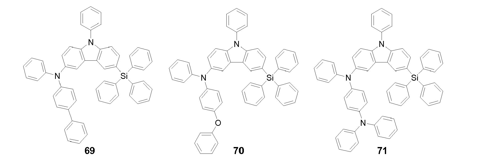
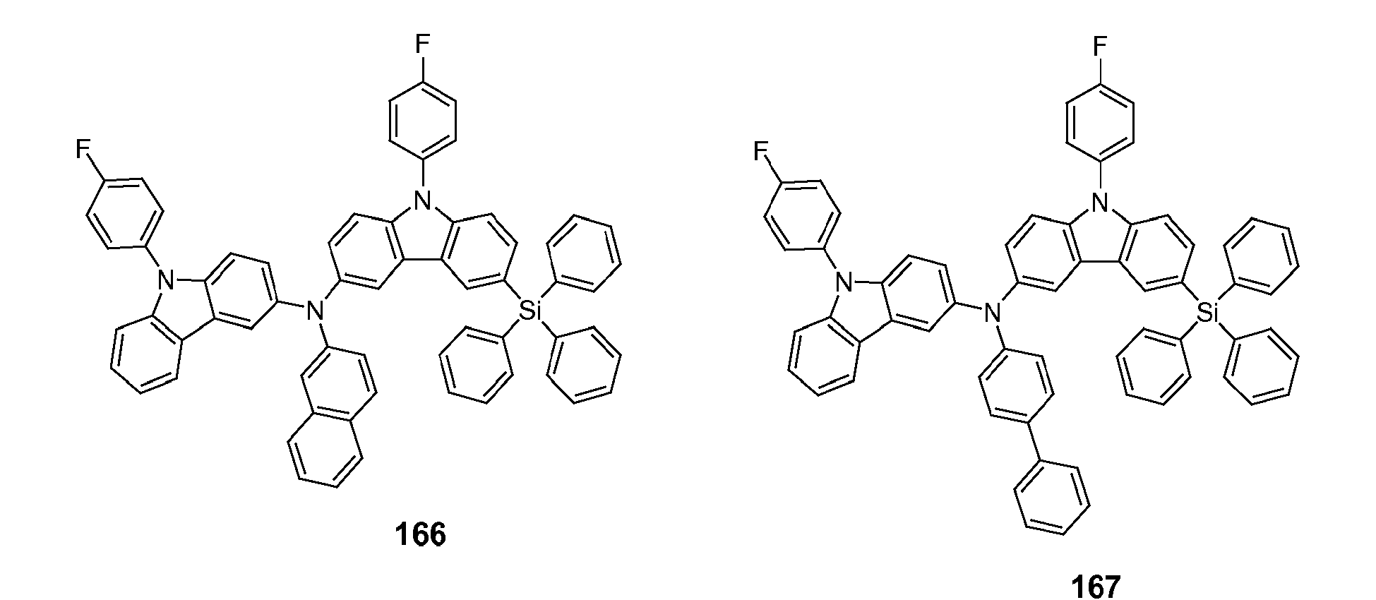
- Preferred examples of suitable silanylamine-based compounds satisfying Formula I include Compounds 1 to 168 below.
- the silanylamine-based compound represented by Formula I may be prepared by various methods. According to a preferred embodiment of the present invention, as shown in Reaction Scheme 1 below, a compound represented by Formula 1 a is reacted with a compound represented by Formula 1b to prepare a silanylamine-based compound represented by Formula I.
- X, n, Ar 1 , Ar 2 , R 1 , R 2 and R 3 are as described above, and Y is a halogen atom such as F, Cl, Br or I.
- the reaction represented by Reaction Scheme 1 may be performed in the presence of Pd 2 (dba) 3 (where dba is dibenzylideneacetone), sodium tert-butoxide and tri(tert-butyl)phosphine and may be performed at a temperature ranging from about 50 to about 150°C.
- an organic light emitting device includes a first electrode, a second electrode and an organic layer positioned between the first electrode and the second electrode.
- the organic layer includes a silanylamine-based compound represented by Formula I.
- the organic layer including the silanylamine-based compound represented by Formula I may be a hole injection layer, a hole transport layer, or a single layer having both hole injection and hole transport capabilities.
- the organic layer including the silanylamine-based compound represented by Formula I may also be an emissive layer.
- the emissive layer may in addition include phosphorescent materials or fluorescent materials.
- the first electrode may be an anode and the second electrode may be a cathode, or the first electrode may be a cathode and the second electrode may be an anode.
- the organic light emitting device may further include at least one layer selected from a hole injection layer, a hole transport layer, an electron blocking layer, an emissive layer, a hole blocking layer, an electron transport layer and an electron injection layer.
- the organic light emitting device may have a first electrode/hole injection layer/emissive layer/second electrode structure, a first electrode/hole injection layer/hole transport layer/emissive layer/ electron transport layer/second electrode structure, or a first electrode/hole injection layer/hole transport layer/emissive layer/electron transport layer/electron injection layer/second electrode structure.
- the organic light emitting device may also have a first electrode/single layer/emissive layer/electron transport layer/second electrode structure, or a first electrode/single layer/emissive layer/electron transport layer/electron injection layer/second electrode structure, where the single layer has both hole injection and hole transport capabilities.
- FIG. 1 is a schematic showing an organic light emitting device according to one embodiment of the present invention.
- the organic light emitting device illustrated in FIG. 1 includes a substrate, a first electrode (anode), a hole injection layer, a hole transport layer, an emissive layer, an electron transport layer, an electron injection layer and a second electrode (cathode).
- the first electrode is first formed by depositing or sputtering a high work-function material on a substrate.
- the first electrode may be an anode or a cathode.
- the substrate can be any substrate used in conventional organic light emitting devices, and may be a glass substrate or a transparent plastic substrate that is waterproof and has excellent mechanical strength, thermal stability, transparency, surface smoothness and ease of handling.
- suitable materials for forming the first electrode include ITO, IZO, SnO 2 , ZnO, Al, Ag, Mg, and any material with high conductivity.
- the hole injection layer may be formed on the first electrode by vacuum deposition, spin coating, casting, Langmuir Blodgett (LB) deposition, or the like.
- the deposition conditions may vary depending on the compound used to form the HIL, and the structure and thermal properties of the HIL to be formed.
- the vacuum deposition conditions may include a deposition temperature ranging from about 100 to about 500°C, a pressure ranging from about 10 -8 to about 10 -3 torr, a deposition velocity ranging from about 0.01 to about 100 ⁇ /sec, and a layer thickness ranging from about 10 ⁇ to 5 ⁇ m.
- the coating conditions may vary depending on the compound used to form the HIL, and the structure and thermal properties of the HIL to be formed. In general, however, the coating velocity may range from about 2000 to about 5000 rpm, and the heat treatment temperature (performed to remove solvent after coating) may range from about 80 to about 200°C.
- the material used to form the HIL may be a silanylamine-based compound represented by Formula I or may be a material known in the art.
- suitable materials for the HIL include phthalocyanine compounds (such as a copper phthalocyanine), star-burst type amine derivatives (such as TCTA, m-MTDATA, and m-MTDAPB), polyaniline/dodecylbenzenesulfonic acid (Pani/DBSA), poly(3,4-ethylenedioxythiophene)/poly(4-styrenesulfonate) (PEDOT/PSS), polyaniline/camphor sulfonic acid (Pani/CSA), (polyaniline)/poly(4-styrenesulfonate) (PANI/PSS) and similar soluble and conductive polymers.
- phthalocyanine compounds such as a copper phthalocyanine
- star-burst type amine derivatives such as TCTA, m-MTDATA,
- the thickness of the HIL may range from about 100 to about 10000 ⁇ . In one embodiment, for example, the thickness of the HIL ranges from about 100 to about 1000 ⁇ . When the thickness of the HIL is within these ranges, excellent hole injecting capabilities and driving voltages of the organic light emitting device may be obtained.
- the hole transport layer may be formed on the HIL by vacuum deposition, spin coating, casting, LB deposition, or the like.
- HTL hole transport layer
- deposition and coating conditions are similar to those for formation of the HIL, although the deposition and coating conditions may vary depending on the compound used to form the HTL.
- the material used to form the HTL may be a silanylamine-based compound represented by Formula I, or a material known in the art.
- suitable materials for forming the HTL include carbazole derivatives (such as N-phenylcarbazole, polyvinylcarbazole and the like), conventional amine derivatives having aromatic condensation rings (such as 4,4'-bis[N-(1-naphthyl)-N-phenylamino]biphenyl (NPB), N,N'-bis(3-methylphenyl)-N,N'-diphenyl-[1,1-biphenyl]-4,4'-diamine (TPD), and N,N'-di(naphthalene-1-yl)-N,N'-diphenyl benzydine ( ⁇ -NPD)), and the like.
- carbazole derivatives such as N-phenylcarbazole, polyvinylcarbazole and the like
- the thickness of the HTL may range from about 50 to about 1000 ⁇ . In one embodiment, for example, the thickness of the HTL ranges from about 100 to about 600 ⁇ . When the thickness of the HTL is within these ranges, excellent hole transporting capabilities and driving voltages of the organic light emitting device may be obtained.
- the emissive layer may be formed on the HTL by vacuum deposition, spin coating, casting, LB, or the like.
- deposition and coating conditions are similar to those for formation of the HIL, although the deposition and coating conditions may vary depending on the compound used to form the EML.
- the material used to form the EML may be a silanylamine-based compound represented by Formula I or various light emitting materials, such as hosts and dopants that are known in the art.
- the dopants may be fluorescent and/or phosphorescent dopants that are known in the art.
- Nonlimiting examples of suitable host materials include Alq 3 , 4,4'-N,N'-dicarbazole-biphenyl (CBP), poly(n-vinylcarbazole) (PVK), distyrylarylene (DSA), or IDE215 from Idemitsu Co.
- CBP 4,4'-N,N'-dicarbazole-biphenyl
- PVK poly(n-vinylcarbazole)
- DSA distyrylarylene
- IDE215 from Idemitsu Co.
- Nonlimiting examples of suitable fluorescent dopants include IDE102, IDE105 and IDE118 from Idemitsu Co.
- suitable phosphorescent dopants include Ir(ppy) 3 (green, where ppy is 2-phenylpyridine) (green), (4,6-F2ppy) 2 lrpic, TEB002 from Covion Co., platinum(II) octaethylporphyrin (PtOEP), compounds represented by Formula 5 below, Firpic, and red phosphorescent dopant RD 61 from UDC Co.
- the amount of the dopant may range from about 0.1 to 20 parts by weight based on 100 parts by weight of the material used to form the EML (i.e., based on 100 parts by weight of the host and the dopant). In one embodiment, for example, the amount of the dopant ranges from about 0.5 to about 12 parts by weight based on 100 parts by weight of the material used to form the EML. When the amount of the dopant is greater than about 0.1 parts by weight, the effect achieved by adding the dopant is sufficient. Also, when the amount of the dopant is less than about 20 parts by weight, fluorescence or phosphorescence quenching may be prevented.
- the thickness of the EML may range from about 100 to about 1000 ⁇ . In one embodiment, for example, the thickness of the EML ranges from about 200 to about 600 ⁇ . When the thickness of the EML is within these ranges, excellent emitting abilities of the EML, and driving voltages of the organic light emitting device may be obtained.
- a hole blocking layer (not shown) may be formed on the EML to prevent diffusion of triplet excitons or holes into the electron transport layer.
- suitable materials for forming the HBL include oxadiazole derivatives, triazole derivatives, phenanthroline derivatives, Balq, and BCP.
- the thickness of the HBL may range from about 50 to about 1000 ⁇ . In one embodiment, for example, the thickness of the HBL ranges from about 100 to about 300 ⁇ . When the thickness of the HBL is within these ranges, excellent hole blocking abilities of the HBL and driving voltages of the organic light emitting device may be obtained.
- the electron transport layer may be formed on the HBL by vacuum deposition, spin coating, casting, or the like.
- deposition and coating conditions are similar to those for formation of the HIL, although the deposition and coating conditions may vary depending on the compound used to form the ETL.
- Nonlimiting examples of suitable materials for forming the ETL include quinoline derivatives (for example, tris(8-quinolinorate)aluminum (Alq 3 )), TAZ, and the like.
- the thickness of the ETL may range from about 100 to about 1000 ⁇ . In one embodiment, for example, the thickness of the ETL ranges from about 100 to about 500 ⁇ . When the thickness of the ETL is within these ranges, excellent electron transporting abilities of the ETL and driving voltages of the organic light emitting device may be obtained.
- the electron injection layer may be formed on the ETL for example, by vacuum deposition, spin coating, casting, or the like.
- the EIL is formed of a material that allows easy injection of electrons from a cathode.
- Nonlimiting examples of suitable materials for forming the EIL include LiF, NaCl, CsF, Li 2 O, BaO, and the like.
- Deposition and coating conditions are similar to those for formation of the HIL, although the deposition and coating conditions may vary depending on the material used to form the EIL.
- the thickness of the EIL may range from about 1 to about 100 ⁇ . In one embodiment, for example, the thickness of the EIL ranges from about 5 to about 90 ⁇ . When the thickness of the EIL is within these ranges, excellent electron injection abilities of the EIL and driving voltages of the organic light emitting device may be obtained.
- the second electrode can be formed on the EIL by vacuum deposition, sputtering, or the like.
- the second electrode can be used as a cathode or an anode.
- the material used to form the second electrode may be a low work-function metal, alloy, electrically conductive compound, or a combination thereof.
- suitable materials for the second electrode include Li, Mg, Al, Al-Li, Ca, Mg-In, Mg-Ag, and the like.
- a transparent cathode formed of ITO or IZO can be used to produce a front surface light emitting device.
- Deposition temperature (Td) and glass transition temperature (Tg) were measured by performing thermal analysis using thermo gravimetric analysis (TGA) and differential scanning calorimetry (DSC) under the following conditions: N 2 atmosphere, temperatures of room temperature to 600 (10 /min) for TGA and room temperature to 400 for DSC, and Pan Type: Pt Pan in disposable Al Pan (TGA) and disposable Al pan (DSC). Td was 330°C, and Tg was 97°C.
- the highest occupied molecular orbital (HOMO) and lowest occupied molecular orbital (LUMO) were measured using the UV absorption spectrum and an ionization potential measurement AC-2.
- the HOMO was 5.4 eV and the LUMO was 2.33 eV.
- Td and Tg were measured by performing thermal analysis using thermo gravimetric analysis (TGA) and differential scanning calorimetry (DSC) under the following conditions: N 2 atmosphere, temperatures of room temperature to 600 (10°C/min) for TGA and of room temperature to 400 for DSC, and Pan Type: Pt Pan in disposable Al Pan (TGA) and disposable Al pan (DSC). Td was 380°C, and Tg was 127°C.
- TGA thermo gravimetric analysis
- DSC differential scanning calorimetry
- the HOMO and LUMO were measured using the UV absorption spectrum and an ionization potential measurement AC-2.
- the HOMO was 5.30 eV and the LUMO was 2.24 eV.
- Td and Tg were measured by performing thermal analysis using thermo gravimetric analysis (TGA) and differential scanning calorimetry (DSC) under the following conditions: N 2 atmosphere, temperatures of room temperature to 600 (10°C/min) for TGA and of room temperature to 400 for DSC, and Pan Type: Pt Pan in disposable Al Pan (TGA) and disposable Al pan(DSC). Td was 414°C, and Tg was 129°C.
- TGA thermo gravimetric analysis
- DSC differential scanning calorimetry
- the HOMO and LUMO were measured using the UV absorption spectrum and an ionization potential measurement AC-2.
- the HOMO was 5.20 eV and the LUMO was 2.21 eV.
- Td and Tg were measured by performing thermal analysis using thermo gravimetric analysis (TGA) and differential scanning calorimetry (DSC) under the following conditions: N 2 atmosphere, temperatures of room temperature to 600 (10°C/min) for TGA and of room temperature to 400 for DSC, and Pan Type: Pt Pan in disposable Al Pan (TGA) and disposable Al pan(DSC). Td was 405°C, and Tg was 126°C.
- TGA thermo gravimetric analysis
- DSC differential scanning calorimetry
- the HOMO and LUMO were measured using the UV absorption spectrum and an ionization potential measurement AC-2.
- the HOMO was 5.20 eV and the LUMO was 2.22 eV.
- Td and Tg were measured by performing thermal analysis using thermo gravimetric analysis (TGA) and differential scanning calorimetry (DSC) under the following conditions: N 2 atmosphere, temperatures of room temperature to 600 (10°C/min) for TGA and of room temperature to 400 for DSC, and Pan Type: Pt Pan in disposable Al Pan (TGA) and disposable Al pan (DSC). Td was 390°C, and Tg was 148°C.
- TGA thermo gravimetric analysis
- DSC differential scanning calorimetry
- the HOMO and LUMO were measured using the UV absorption spectrum and an ionization potential measurement AC-2.
- the HOMO was 5.1 eV and the LUMO was 2.15 eV.
- a corning 15 ⁇ /cm 2 (1,200 ⁇ ) ITO glass substrate was cut into 50mm x 50mm x 0.7mm size pieces, ultrasonicwashed with isopropyl alcohol for 5 minutes, ultrasonicwashed with deionized water for 5 minutes, and washed with UV ozone for 30 minutes. Then, the glass substrate was installed in a vacuum deposition device.
- Compound 9 was vacuum deposited on the substrate to form a HIL with a thickness of 600 ⁇ .
- 4,4'-bis[N-(1-naphthyl)-N-phenylamino]biphenyl (NPB) was vacuum deposited on the HIL to form a HTL with a thickness of 300 ⁇ .
- IDE215 (a blue fluorescent host obtained from Idemitsu Co.) and IDE118 (a blue fluorescent dopant obtained from Idemitsu Co.) (98:2, w/w) were vacuum deposited on the HTL to form an EML with a thickness of 300 ⁇ .
- Alq 3 was vacuum deposited on the EML to form an ETL with a thickness of 300 ⁇
- LiF was vacuum deposited on the ETL to form an EIL with a thickness of 10 ⁇
- Al was vacuum deposited on the EIL to a thickness of 3000 ⁇ (cathode) to form a LiF/Al electrode to complete the manufacture of an organic light emitting device.
- An organic light emitting device was prepared as in Example 1, except that Compound 43 was used instead of Compound 9 in forming the HIL.
- An organic light emitting device was prepared as in Example 1, except that Compound 44 was used instead of Compound 9 in forming the HIL.
- An organic light emitting device was prepared as in Example 1, except that Compound 45 was used instead of Compound 9 in forming the HIL.
- An organic light emitting device was prepared as in Example 1, except that Compound 137 was used instead of Compound 9 in forming the HIL.
- An organic light emitting device was prepared as in Example 1, except that IDE406 (from Idemitsu Co.) was used instead of Compound 9 in forming the HIL.
- FIG. 2 is a graph of luminance according to driving voltage of the organic light emitting devices according to Example 1 and Comparative Example 1
- FIG. 3 is a graph of luminance according to driving voltage of the organic light emitting devices according to Example 2 and Comparative Example 1
- FIG. 4 is a graph of luminance according to time (100mA/cm 2 ) of the organic light emitting devices according to Example 3 and Comparative Example 1.
- the organic light emitting devices prepared according to Examples 1 to 5 had better I-V-L characteristics compared to the organic light emitting device prepared according to Comparative Example 1.
- the organic light emitting device of Example 1 having an organic layer including Compound 9 as the HIL, and the organic light emitting device of Example 2 having an organic layer including Compound 43 as the HIL showed improved brightness compared to the organic light emitting device of Comparative Example 1 (Refer to FIGS. 2 and 3).
- the organic light emitting devices of Examples 1 to 5 had similar color coordinate characteristics to that of Comparative Example 1.
- the organic light emitting device of Example 3 had a longer lifetime than that of Comparative Example 1.
- the silanylamine-based compounds according to the present invention have excellent electrical stability and high hole transporting capabilities.
- the silanylamine-based compounds of the present invention may be effectively used for red, green, blue, and white fluorescent and phosphorescent materials used to form HILs, HTLs, and EMLs in organic light emitting devices.
- Organic light emitting devices having high efficiency, low driving voltage, high brightness and long lifetime may be prepared using the silanylamine-based compounds of the present invention.
Landscapes
- Chemical & Material Sciences (AREA)
- Organic Chemistry (AREA)
- Electroluminescent Light Sources (AREA)
- Indole Compounds (AREA)
Abstract
Description
- The present invention relates to silanylamine-based compounds, methods of preparing the same, and organic light emitting devices including organic layers comprising a silanylamine-based compound.
- Organic light emitting devices (OLEDS) are self-emitting devices having wide viewing angles, excellent contrast, and quick responses. Organic light emitting devices have low operating voltages and quick response times, and can realize multi-color images. Accordingly, OLEDs are being extensively researched.
- A typical organic light emitting device has an anode/emissive layer/cathode structure. Organic light emitting devices can also have various other structures, such as anode/hole transport layer/emissive layer/cathode, and anode/hole transport layer/emissive layer/electron injection layer/cathode. These alternative structures are realized by further including an electron transport layer and at least one of a hole injection layer, a hole transport layer and an electron injection layer between the anode and the emissive layer, or between the emissive layer and the cathode.
- Fluorene and anthracene derivatives have been used as to form the hole transport layer. However, organic light emitting devices having these hole transport layers do not have satisfactory lifetime, efficiency, and power consumption.
- According to one aspect of the present invention, a silanylamine-based compound represented by Formula I below is provided.

n is an integer ranging from 0 to 5;
Ar1 and Ar2 are each independently selected from the group consisting of hydrogen, substituted or unsubstituted C6-C30 aryl groups, substituted or unsubstituted C2-C30 heteroaryl groups; and
R1, R2 and R3 are each independently selected from the group consisting of hydrogen, substituted or unsubstituted C1-C30 alkyl groups, substituted or unsubstituted C2-C30 alkenyl groups, substituted or unsubstituted C2-C30 alkynyl groups, substituted or unsubstituted C1-C30 alkoxy groups, substituted or unsubstituted C6-C30 aryloxy groups, substituted or unsubstituted C6-C30 aryl groups and substituted or unsubstituted C2-C30 heteroaryl groups, wherein at least two of R1, R2 and R3 may be bonded to each other to form a saturated or unsaturated ring. - According to another embodiment of the present invention, a method of preparing a silanylamine-based compound represented by Formula I is provided. The method includes reacting a compound represented by Formula 1a and a compound represented by Formula 1 b via
Reaction Scheme 1 below.
- According to another embodiment of the present invention, an organic light emitting device includes a first electrode, a second electrode, and an organic layer positioned between the first electrode and the second electrode, the organic layer including the silanylamine-based compound of formula I. The organic light emitting device including the silanylamine-based compound represented by Formula I exhibits low driving voltage, excellent luminance, high efficiency, high current density and has a long lifetime.
- The above and other features and advantages of the present invention will become more apparent by reference to the following detailed description when considered in conjunction with the attached drawings in which:
- FIG. 1 is a schematic illustrating an organic light emitting device according to one embodiment of the present invention;
- FIG. 2 is a graph of luminance according to driving voltage of organic light emitting devices prepared according to Example 1 and Comparative Example 1;
- FIG. 3 is a graph of luminance according to driving voltage of organic light emitting devices prepared according to Example 2 and Comparative Example 1; and
- FIG. 4 is a graph of luminance according to time of organic light emitting devices prepared according to Example 3 and Comparative Example 1.
- According to one embodiment of the present invention, a silanylamine-based compound is represented by Formula I below.

- In Formula I, n may be an integer ranging from 0 to 5, preferably from 1 to 5, and X may be selected from substituted and unsubstituted C1-C30 alkylene groups, substituted and unsubstituted C6-C30 arylene groups, and substituted and unsubstituted C2-C30 heteroarylene groups. Ar1 and Ar2 may be each independently selected from hydrogen atoms, substituted and unsubstituted C6-C30 aryl groups, and substituted and unsubstituted C2-C30 heteroaryl groups. R1, R2 and R3 may be each independently selected from hydrogen atoms, substituted and unsubstituted C1-C30 alkyl groups, substituted and unsubstituted C2-C30 alkenyl groups, substituted and unsubstituted C2-C30 alkynyl groups, substituted and unsubstituted C1-C30 alkoxy groups, substituted and unsubstituted C6-C30 aryloxy groups, substituted and unsubstituted C6-C30 aryl groups, and substituted and unsubstituted C2-C30 heteroaryl groups. At least two of R1, R2 and R3 may be bonded to each other to form a saturated or unsaturated ring.
- Preferrred examples of suitable unsubstituted C1-C30 alkyl groups of R1 to R3 include methyl, ethyl, propyl, isobutyl, sec-butyl, pentyl, iso-amyl, and hexyl. At least one of the hydrogen atoms in the mentioned alkyl groups may be substituted with a constituent selected from halogen, hydroxy, nitro, cyano, amino groups, amidino groups, hydrazines, hydrazones, carboxyl and salts thereof, sulfonic acid and salts thereof, phosphoric acid and salts thereof, C1-C30 alkenyl groups, C1-C30 alkynyl groups, C6-C30 aryl groups, C7-C20 arylalkyl groups, C2-C20 heteroaryl groups, C3-C30 heteroarylalkyl groups, C6-C30 aryloxy groups and -N(Z1)(Z2). In the -N(Z1)(Z2) substituent, Z1 and Z2 may be each independently selected from hydrogen, substituted and unsubstituted C1-C30 alkyl groups, substituted and unsubstituted C1-C30 haloalkyl groups, substituted and unsubstituted C6-C30 aryl groups, substituted and unsubstituted C6-C30 haloaryl groups, and substituted and unsubstituted C2-C30 heteroaryl groups.
- The unsubstituted C1-C30 alkylene group of the linking group X is a bivalent linking group having a structure similar to an alkyl group, and preferred examples of the alkylene group include methylene groups and ethylene groups. At least one hydrogen atom in the alkylene group may be substituted with any of the substituents described above in connection with the unsubstituted C1-C30 alkyl group.
- Preferred examples of the unsubstituted C1-C30 alkoxy group of R1 to R3 include methoxy groups, ethoxy groups, phenyloxy groups, cyclohexyloxy groups, naphthyloxy groups, isopropyloxy groups, and diphenyloxy groups. At least one of the hydrogen atoms in the alkoxy group may be substituted with any of the substituents described above in connection with the unsubstituted C1-C30 alkyl group.
- The C2-C30 alkenyl group of the linking group X is a hydrocarbon chain having a carbon-carbon double bond in the center or at one end of the alkyl group structure. Preferred examples of suitable alkenyl groups include ethylene groups, propylene groups, butylene groups, and hexylene groups. At least one hydrogen atom in the alkenyl group may be substituted with any substituent described above in connection with the unsubstituted C1-C30 alkyl group.
- The C2-C30 alkynyl group of R1 to R3 is a hydrocarbon chain having a carbon-carbon triple bond in the center or at one end of the alkyl group structure. Preferred examples of suitable alkynyl groups include acetylene groups, propylacetylene groups, phenylacetylene groups, naphthylacetylene groups, isopropylacetylene groups, t-butylacetylene groups, and diphenylacetylene groups. At least one of the hydrogen atoms in the alkynyl group may be substituted with any substituent described above in connection with the unsubstituted C1-C30 alkyl group.
- The C6-C30 aryl group of R1 to R3 as well as Ar1 and Ar2 is a carbocyclic aromatic system having from 6 to 30 carbon atoms and including at least one aromatic ring. The rings can be fused to each other or bonded to each other, for example, through a single bond. At least one hydrogen atom in the aryl group may be substituted with any of the substituents described above in connection with the unsubstituted C1-C30 alkyl group.
- Nonlimiting Preferred examples of suitable substituted or unsubstituted C6-C30 aryl groups include phenyl groups, C1-C10 alkylphenyl groups (e.g., ethylphenyl groups), halophenyl groups (e.g., o-, m- and p-fluorophenyl groups, and dichlorophenyl groups), cyanophenyl groups, dicyanophenyl groups, trifluoromethoxyphenyl groups, biphenyl groups, halobiphenyl groups, cyanobiphenyl groups, C1-C10 biphenyl groups, C1-C10 alkoxybiphenyl groups, o-, m-and p-tolyl groups, o-, m- and p-cumenyl groups, mesityl groups, phenoxyphenyl groups, (α,α-dimethylbenzen)phenyl groups, (N,N'-dimethyl)aminophenyl groups, (N,N'-diphenyl)aminophenyl groups, pentalenyl groups, indenyl groups, naphthyl groups, halonaphthyl groups (e.g., fluoronaphthyl groups), C1-C10 alkylnaphthyl groups (e.g., methylnaphthyl groups), C1-C10 alkoxynaphthyl groups (e.g., methoxynaphthyl groups), cyanonaphthyl groups, anthracenyl groups, azulenyl groups, heptalenyl groups, acenaphthylenyl groups, phenalenyl groups, fluorenyl groups, anthraquinolyl groups, methylanthryl groups, phenanthrenyl groups, triphenylenyl groups, pyrenyl groups, chrysenyl groups, ethyl-chrysenyl groups, picenyl groups, perylenyl groups, chloroperylenyl groups, pentaphenyl groups, pentacenyl groups, tetraphenylenyl groups, hexaphenyl groups, hexacenyl groups, rubicenyl groups, coronenyl groups, trinaphthylenyl groups, heptaphenyl groups, heptacenyl groups, pyranthrenyl groups, and ovalenyl groups. At least one of the hydrogen atoms in the aryl group may be substituted with any of the substituents described above in connection with the unsubstituted C1-C30 alkyl group.
- The unsubstituted C6-C30 arylene group of the linking group X is a bivalent linking group having a structure similar to the aryl group, and preferred examples of the arylene group include phenylene groups and naphthylene groups. At least one hydrogen atom in the arylene group may be substituted with any of the substituents described above in connection with the unsubstituted C1-C30 alkyl group.
- The unsubstituted C2-C30 heteroaryl group of R1 to R3 as well as Ar1 and Ar2 is a group having at least one aromatic ring in which at least one carbon atom in the aryl group is substituted with one of N, O, P and S. The aromatic rings can be fused to each other or bonded to each other, for example, through a single bond. At least one hydrogen atom in the heteroaryl group may be substituted with any of the substituents described above in connection with the unsubstituted C1-C30 alkyl group.
- Preferred examples of the unsubstituted C2-C30 heteroaryl group include pyrazolyl groups, imidazolyl groups, oxazolyl groups, thiazolyl groups, triazolyl groups, tetrazolyl groups, oxadiazolyl groups, pyridinyl groups, pyridazinyl groups, pyrimidinyl groups, triazinyl groups, carbazolyl groups, indolyl groups, quinolinyl groups, and isoquinolinyl groups. At least one hydrogen atom in the heteroaryl group may be substituted with any of the substituents described above in connection with the unsubstituted C1-C30 alkyl group.
- The unsubstituted C2-C60 heteroarylene group of the linking group X is a bivalent linking group having a structure similar to the heteroaryl group, and at least one hydrogen atom in the heteroarylene group may be substituted with any of the substituents described above in connection with the unsubstituted C1-C30 alkyl group.
- The unsubstituted C6-C30 aryloxy group of R1 to R3 is a group represented by -OA, where A is the aryl group, such as a phenoxy group. At least one hydrogen atom in the aryloxy group may be substituted with any of the substituents described above in connection with the unsubstituted C1-C30 alkyl group.
- According to one embodiment of the present invention, in Formula I, X may be selected from substituted and unsubstituted C1-C10 alkylene groups, substituted and unsubstituted phenylene groups, substituted and unsubstituted naphthylene groups, substituted and unsubstituted fluorenylene groups, substituted and unsubstituted anthracenylene groups, substituted and unsubstituted pyridinylene groups, substituted and unsubstituted quinolylene groups, substituted and unsubstituted isoquinolylene groups, substituted and unsubstituted anthraquinolylene groups, and substituted and unsubstituted carbazolylene groups.
- Preferred examples of suitable substituents for X include structures shown below.


- In the structures shown, R4 and R5 are each independently selected from hydrogen atoms, halogen atoms, cyano groups, hydroxyl groups, substituted and unsubstituted C1-C30 alkyl groups, substituted and unsubstituted C1-C30 alkoxy groups, substituted and unsubstituted C6-C30 aryl groups, and substituted and unsubstituted C2-C30 heteroaryl groups. In one embodiment, for example, R4 and R5 are each independently selected from phenyl groups and halophenyl groups.
- With X and n being as described above, preferred examples of suitable -(X)n- linking groups include the substituents shown below.


- In the structures shown, Ar1 and Ar2 are each independently selected from substituted and unsubstituted C6-C12 aryl groups, and substituted and unsubstituted C2-C15 heteroaryl groups. Preferably, n is 1.
- Preferred examples of suitable substituents for Ar1 and Ar2 include phenyl groups, halophenyl groups, cyanophenyl groups, C1-C5 alkylphenyl groups, C1-C5 alkoxyphenyl groups, phenoxyphenyl groups, phenyl groups substituted with -N(Z1)(Z2), biphenyl groups, halobiphenyl groups, cyanobiphenyl groups, C1-C5 alkylbiphenyl groups, C1-C5 alkoxybiphenyl groups, biphenyl groups substituted with -N(Z1)(Z2), naphthyl groups, halonaphthyl groups, cyanonaphthyl groups, C1-C5 alkylnaphthyl groups, C1-C5 alkoxynaphthyl groups, phenoxynaphthyl groups, naphthyl groups substituted with -N(Z1)(Z2), fluorenyl groups, halofluorenyl groups, cyanofluorenyl groups, C1-C5 alkylfluorenyl groups, C1-C5 alkoxyfluorenyl groups, phenoxyfluorenyl groups, carbazolyl groups, halocarbazolyl groups, cyanocarbazolyl groups, C1-C5 alkylcarbazolyl groups, C1-C5 alkoxycarbazolyl groups, phenoxycarbazolyl groups, carbazolyl groups substituted with -N(Z1)(Z2), C6-C12 arylcarbazolyl groups, C6-C12 haloarylcarbazolyl groups, pyridyl groups, halopyridyl groups, cyanopyridyl groups, C1-C5alkylpyridyl groups, C1-C5alkoxypyridyl groups, phenoxypyridyl groups, and pyridyl groups substituted with -N(Z1)(Z2).
- In the structures shown, preferred examples of suitable substituents for Z1 and Z2 include hydrogen, substituted and unsubstituted C1-C30 alkyl groups, substituted and unsubstituted C1-C30 haloalkyl groups, substituted and unsubstituted C6-C30 aryl groups, substituted and unsubstituted C6-C30 haloaryl groups, and substituted and unsubstituted C2-C30 heteroaryl groups. In one embodiment, Z1 and Z2 are each independently selected from C6-C12 aryl groups, and C6-C12 haloaryl groups.
- Preferred examples of suitable substituents for Ar1 and Ar2 include those represented below. m may be an integer ranging from 1 to 5, preferably m is 1.


- Preferably, R1, R2 and R3 may be each independently selected from substituted and unsubstituted C1-C10 alkyl groups, substituted and unsubstituted C1-C10 alkoxy groups, substituted and unsubstituted C6-C12 aryl groups, substituted and unsubstituted C6-C12 aryloxy groups, and substituted and unsubstituted C2-C12 heteroaryl groups. Preferred examples of suitable substituents for R1, R2 and R3 include C1-C10 alkyl groups, phenyl groups, halophenyl groups, cyanophenyl groups, C1-C10 alkylphenyl groups, C1-C10 alkoxyphenyl groups, biphenyl groups, halobiphenyl groups, naphthyl groups, halonaphthyl groups, C1-C10 alkylnaphthyl groups, and C1-C10 alkoxynaphthyl groups.
- Preferably, X is selected from the group consisting of

- Preferred examples of suitable silanylamine-based compounds satisfying Formula I include
Compounds 1 to 168 below.





- The silanylamine-based compound represented by Formula I may be prepared by various methods. According to a preferred embodiment of the present invention, as shown in
Reaction Scheme 1 below, a compound represented by Formula 1 a is reacted with a compound represented by Formula 1b to prepare a silanylamine-based compound represented by Formula I.
- The reaction represented by
Reaction Scheme 1 may be performed in the presence of Pd2(dba)3 (where dba is dibenzylideneacetone), sodium tert-butoxide and tri(tert-butyl)phosphine and may be performed at a temperature ranging from about 50 to about 150°C. - According to another embodiment of the present invention, an organic light emitting device includes a first electrode, a second electrode and an organic layer positioned between the first electrode and the second electrode. The organic layer includes a silanylamine-based compound represented by Formula I. The organic layer including the silanylamine-based compound represented by Formula I may be a hole injection layer, a hole transport layer, or a single layer having both hole injection and hole transport capabilities. The organic layer including the silanylamine-based compound represented by Formula I may also be an emissive layer. The emissive layer may in addition include phosphorescent materials or fluorescent materials. The first electrode may be an anode and the second electrode may be a cathode, or the first electrode may be a cathode and the second electrode may be an anode.
- The organic light emitting device may further include at least one layer selected from a hole injection layer, a hole transport layer, an electron blocking layer, an emissive layer, a hole blocking layer, an electron transport layer and an electron injection layer. For example, the organic light emitting device may have a first electrode/hole injection layer/emissive layer/second electrode structure, a first electrode/hole injection layer/hole transport layer/emissive layer/ electron transport layer/second electrode structure, or a first electrode/hole injection layer/hole transport layer/emissive layer/electron transport layer/electron injection layer/second electrode structure. The organic light emitting device may also have a first electrode/single layer/emissive layer/electron transport layer/second electrode structure, or a first electrode/single layer/emissive layer/electron transport layer/electron injection layer/second electrode structure, where the single layer has both hole injection and hole transport capabilities.
- Hereinafter, a method of preparing an organic light emitting device according to one embodiment of the present invention will be described with reference to FIG. 1. FIG. 1 is a schematic showing an organic light emitting device according to one embodiment of the present invention. The organic light emitting device illustrated in FIG. 1 includes a substrate, a first electrode (anode), a hole injection layer, a hole transport layer, an emissive layer, an electron transport layer, an electron injection layer and a second electrode (cathode).
- The first electrode is first formed by depositing or sputtering a high work-function material on a substrate. The first electrode may be an anode or a cathode. The substrate can be any substrate used in conventional organic light emitting devices, and may be a glass substrate or a transparent plastic substrate that is waterproof and has excellent mechanical strength, thermal stability, transparency, surface smoothness and ease of handling. Nonlimiting examples of suitable materials for forming the first electrode include ITO, IZO, SnO2, ZnO, Al, Ag, Mg, and any material with high conductivity.
- Then, the hole injection layer (HIL) may be formed on the first electrode by vacuum deposition, spin coating, casting, Langmuir Blodgett (LB) deposition, or the like.
- When the HIL is formed using vacuum deposition, the deposition conditions may vary depending on the compound used to form the HIL, and the structure and thermal properties of the HIL to be formed. In general, however, the vacuum deposition conditions may include a deposition temperature ranging from about 100 to about 500°C, a pressure ranging from about 10-8 to about 10-3 torr, a deposition velocity ranging from about 0.01 to about 100 Å/sec, and a layer thickness ranging from about 10 Å to 5 µm.
- When the HIL is formed by spin coating, the coating conditions may vary depending on the compound used to form the HIL, and the structure and thermal properties of the HIL to be formed. In general, however, the coating velocity may range from about 2000 to about 5000 rpm, and the heat treatment temperature (performed to remove solvent after coating) may range from about 80 to about 200°C.
- The material used to form the HIL may be a silanylamine-based compound represented by Formula I or may be a material known in the art. Nonlimiting examples of suitable materials for the HIL include phthalocyanine compounds (such as a copper phthalocyanine), star-burst type amine derivatives (such as TCTA, m-MTDATA, and m-MTDAPB), polyaniline/dodecylbenzenesulfonic acid (Pani/DBSA), poly(3,4-ethylenedioxythiophene)/poly(4-styrenesulfonate) (PEDOT/PSS), polyaniline/camphor sulfonic acid (Pani/CSA), (polyaniline)/poly(4-styrenesulfonate) (PANI/PSS) and similar soluble and conductive polymers.

- The thickness of the HIL may range from about 100 to about 10000Å. In one embodiment, for example, the thickness of the HIL ranges from about 100 to about 1000Å. When the thickness of the HIL is within these ranges, excellent hole injecting capabilities and driving voltages of the organic light emitting device may be obtained.
- Then, the hole transport layer (HTL) may be formed on the HIL by vacuum deposition, spin coating, casting, LB deposition, or the like. When the HTL is formed by vacuum deposition or spin coating, deposition and coating conditions are similar to those for formation of the HIL, although the deposition and coating conditions may vary depending on the compound used to form the HTL.
- The material used to form the HTL may be a silanylamine-based compound represented by Formula I, or a material known in the art. Nonlimiting examples of suitable materials for forming the HTL include carbazole derivatives (such as N-phenylcarbazole, polyvinylcarbazole and the like), conventional amine derivatives having aromatic condensation rings (such as 4,4'-bis[N-(1-naphthyl)-N-phenylamino]biphenyl (NPB), N,N'-bis(3-methylphenyl)-N,N'-diphenyl-[1,1-biphenyl]-4,4'-diamine (TPD), and N,N'-di(naphthalene-1-yl)-N,N'-diphenyl benzydine (α-NPD)), and the like.

- The thickness of the HTL may range from about 50 to about 1000Å. In one embodiment, for example, the thickness of the HTL ranges from about 100 to about 600Å. When the thickness of the HTL is within these ranges, excellent hole transporting capabilities and driving voltages of the organic light emitting device may be obtained.
- Then, the emissive layer (EML) may be formed on the HTL by vacuum deposition, spin coating, casting, LB, or the like. When the EML is formed by vacuum deposition or spin coating, deposition and coating conditions are similar to those for formation of the HIL, although the deposition and coating conditions may vary depending on the compound used to form the EML.
- The material used to form the EML may be a silanylamine-based compound represented by Formula I or various light emitting materials, such as hosts and dopants that are known in the art. The dopants may be fluorescent and/or phosphorescent dopants that are known in the art.
- Nonlimiting examples of suitable host materials include Alq3, 4,4'-N,N'-dicarbazole-biphenyl (CBP), poly(n-vinylcarbazole) (PVK), distyrylarylene (DSA), or IDE215 from Idemitsu Co.
- Nonlimiting examples of suitable fluorescent dopants include IDE102, IDE105 and IDE118 from Idemitsu Co. Nonlimiting examples of suitable phosphorescent dopants include Ir(ppy)3 (green, where ppy is 2-phenylpyridine) (green), (4,6-F2ppy)2lrpic, TEB002 from Covion Co., platinum(II) octaethylporphyrin (PtOEP), compounds represented by Formula 5 below, Firpic, and red phosphorescent dopant RD 61 from UDC Co.

- The amount of the dopant may range from about 0.1 to 20 parts by weight based on 100 parts by weight of the material used to form the EML (i.e., based on 100 parts by weight of the host and the dopant). In one embodiment, for example, the amount of the dopant ranges from about 0.5 to about 12 parts by weight based on 100 parts by weight of the material used to form the EML. When the amount of the dopant is greater than about 0.1 parts by weight, the effect achieved by adding the dopant is sufficient. Also, when the amount of the dopant is less than about 20 parts by weight, fluorescence or phosphorescence quenching may be prevented.
- The thickness of the EML may range from about 100 to about 1000Å. In one embodiment, for example, the thickness of the EML ranges from about 200 to about 600Å. When the thickness of the EML is within these ranges, excellent emitting abilities of the EML, and driving voltages of the organic light emitting device may be obtained.
- When the EML includes a phosphorescent dopant, a hole blocking layer (HBL) (not shown) may be formed on the EML to prevent diffusion of triplet excitons or holes into the electron transport layer. Nonlimiting examples of suitable materials for forming the HBL include oxadiazole derivatives, triazole derivatives, phenanthroline derivatives, Balq, and BCP.
- The thickness of the HBL may range from about 50 to about 1000 Å. In one embodiment, for example, the thickness of the HBL ranges from about 100 to about 300 Å. When the thickness of the HBL is within these ranges, excellent hole blocking abilities of the HBL and driving voltages of the organic light emitting device may be obtained.
- Then, the electron transport layer (ETL) may be formed on the HBL by vacuum deposition, spin coating, casting, or the like. When the ETL is formed by vacuum deposition or spin coating, deposition and coating conditions are similar to those for formation of the HIL, although the deposition and coating conditions may vary depending on the compound used to form the ETL.
- Nonlimiting examples of suitable materials for forming the ETL include quinoline derivatives (for example, tris(8-quinolinorate)aluminum (Alq3)), TAZ, and the like.
- The thickness of the ETL may range from about 100 to about 1000 Å. In one embodiment, for example, the thickness of the ETL ranges from about 100 to about 500Å. When the thickness of the ETL is within these ranges, excellent electron transporting abilities of the ETL and driving voltages of the organic light emitting device may be obtained.
- Then, the electron injection layer (EIL) may be formed on the ETL for example, by vacuum deposition, spin coating, casting, or the like. The EIL is formed of a material that allows easy injection of electrons from a cathode.
- Nonlimiting examples of suitable materials for forming the EIL include LiF, NaCl, CsF, Li2O, BaO, and the like. Deposition and coating conditions are similar to those for formation of the HIL, although the deposition and coating conditions may vary depending on the material used to form the EIL.
- The thickness of the EIL may range from about 1 to about 100 Å. In one embodiment, for example, the thickness of the EIL ranges from about 5 to about 90Å. When the thickness of the EIL is within these ranges, excellent electron injection abilities of the EIL and driving voltages of the organic light emitting device may be obtained.
- Finally, the second electrode can be formed on the EIL by vacuum deposition, sputtering, or the like. The second electrode can be used as a cathode or an anode. The material used to form the second electrode may be a low work-function metal, alloy, electrically conductive compound, or a combination thereof. Nonlimiting examples of suitable materials for the second electrode include Li, Mg, Al, Al-Li, Ca, Mg-In, Mg-Ag, and the like. In addition, a transparent cathode formed of ITO or IZO can be used to produce a front surface light emitting device.
- Hereinafter, Synthesis Examples of Compounds 9, 43, 44, 45, and 137 and Examples are presented. However, the Synthesis Examples and Examples are presented for illustrative purposes only and are not intended to limit the scope of the present invention.
- Compound 9 was synthesized via
Reaction Scheme 2 below:
- 3.12 g (10 mmol) of dibromobiphenyl was dissolved in 30 mL of THF, and 4mL of 2.5M n-butyllithium (in Hexane) was added thereto at-78 . 2.95 g (10 mmol) of chlorotriphenylsilane dissolved in 5 mL of THF was gradually added thereto at -78 after one hour. The mixture was stirred at room temperature for 5 hours, water was added thereto and the mixture was washed three times with 30 mL of diethylether. The washed diethylether layer was dried over MgSO4 and dried under reduced pressure to obtain a product. The obtained product was purified by silica gel column chromatography to obtain 2.9 g of white solid intermediate A (Yield: 60%). (1H NMR (CDCl3, 400MHz) δ (ppm) 7.65-7.53 (m, 12H), 7.47-7.36 (m, 11H)).
- 4.9 g (10 mmol) of intermediate A, 2.6 g (12 mmol) of 2-naphthylphenylamine, 2.9 mg (30 mmol) of t-BuONa, 183 mg (0.2 mmol) of Pd2(dba)3, 40 mg (0.2 mmol) of P(t-Bu)3 were dissolved in 40 mL of toluene and stirred at 90°C for three hours.
- When the reaction was completed, the mixture was cooled to room temperature and extracted three times with 40 mL of distilled water and diethylether. A collected organic layer was dried over MgSO4 to evaporate the solvent. The residue was purified using silica gel column chromatography to obtain 5.67 g of yellow solid Compound 9 (Yield: 90%). (1H NMR (CD2Cl2, 400MHz) δ (ppm) 7.75 (t, 2H), 7.63-7.56 (m, 12H), 7.53 (d, 2H), 7.46-7.34 (m, 12 H), 7.30-7.26 (m, 3H), 7.16 (d, 4H), 7.06 (t, 1 H); 13C NMR (CD2Cl2, 100MHz) δ (ppm) 147.6, 147.5, 145.3, 141.7, 136.9, 136.3, 134.8, 134.5, 134.2, 132.4, 130.2, 129.7, 129.4, 128.9, 127.9, 127.8, 127.5, 126.9, 126.3, 126.0, 124.8, 124.6, 124.5, 124.0, 123.3, 120.5).
- The UV absorption spectrum of 0.2 mM of the obtained Compound 9 diluted in CH2Cl2 was measured, and the maximum absorption spectrum was 340 nm.
- Deposition temperature (Td) and glass transition temperature (Tg) were measured by performing thermal analysis using thermo gravimetric analysis (TGA) and differential scanning calorimetry (DSC) under the following conditions: N2 atmosphere, temperatures of room temperature to 600 (10 /min) for TGA and room temperature to 400 for DSC, and Pan Type: Pt Pan in disposable Al Pan (TGA) and disposable Al pan (DSC). Td was 330°C, and Tg was 97°C.
- The highest occupied molecular orbital (HOMO) and lowest occupied molecular orbital (LUMO) were measured using the UV absorption spectrum and an ionization potential measurement AC-2. The HOMO was 5.4 eV and the LUMO was 2.33 eV.
- Compound 43 was synthesized via
Reaction Scheme 3 below: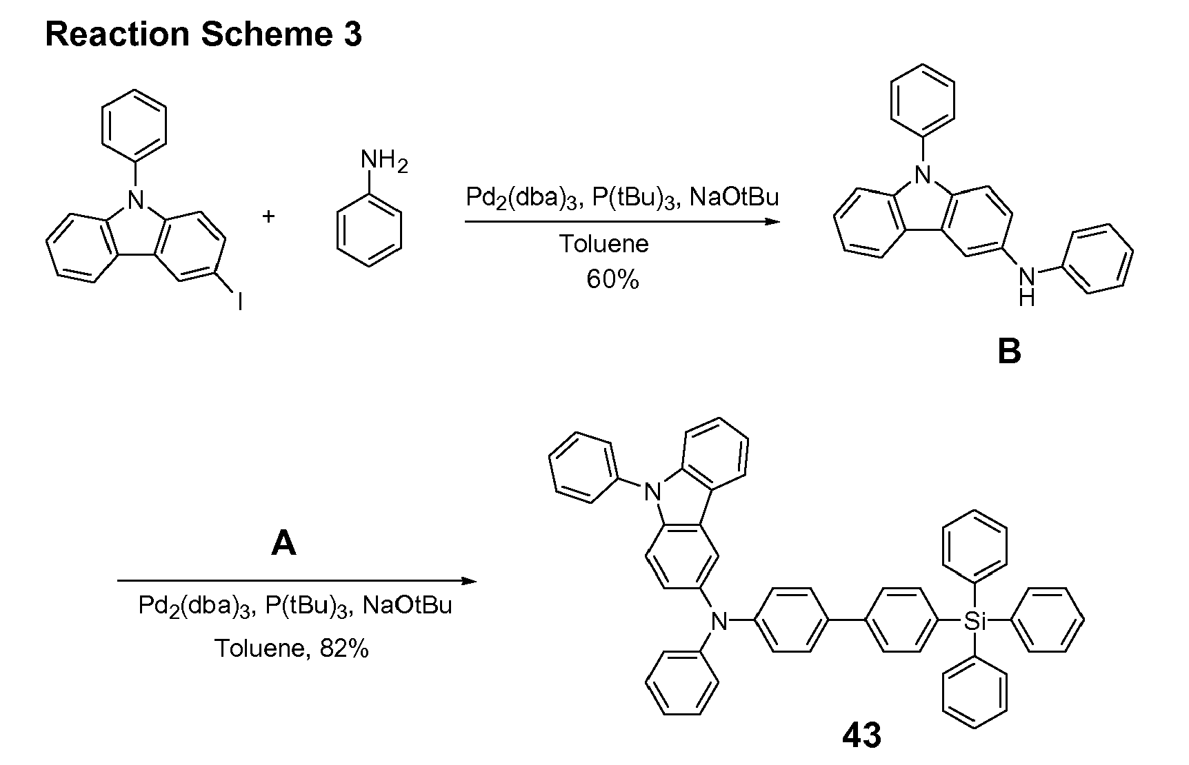
- 3.69 g (10.0 mmol) of 3-iodo-9-phenylcarbazole, 1.11 g (12.0 mmol) of aniline, 2.88 g (30.0 mmol) of t-BuONa, 183 mg (0.2 mmol) of Pd2(dba)3, 40 mg (0.2 mmol) of P(t-Bu)3 were dissolved in 40 mL of toluene, and stirred at 90°C for 3 hours.
- When the reaction was completed, the mixture was cooled to room temperature and distilled water was added thereto. The mixture was extracted three times with 40 mL of diethylether. A collected organic layer was dried over MgSO4 to evaporate the solvent. The residue was purified using silica gel column chromatography to obtain 2.17 g of white solid Intermediate B (Yield: 65 %). (1H NMR (CDCl3, 400MHz) δ (ppm) 8.01 (m, 1 H), 7.66 (m, 1 H), 7.51-7.33 (m, 7H), 7.21-6.94 (m, 5H), 6.73 (m, 1 H), 5.68 (bs, 1 H); 13C NMR (CDCl3, 100MHz) δ (ppm) 144.6, 139.8, 137.4, 135.7, 129.8, 129.3, 128.0, 127.4, 127.1, 126.5, 119.1, 119.0, 118.6, 118.4, 116.7, 113.1, 111.1, 109.4, 102.4).
- Compound 43 was obtained as in Synthesis Example 1, except that Intermediate B was used instead of 2-naphthylphenylamine (Yield: 82%). (1H NMR (CDCl3, 300MHz) δ (ppm) 7.98 (d, 1 H), 7.69 (bd, 1 H), 7.67-7.54 (m, 14H), 7.50-7.33 (m, 14H), 7.28-7.13 (m, 9H), 6.97 (t, 1 H); DEPT 13C NMR (CDCl3, 100MHz) δ (ppm) 136.9, 136.5, 130.0, 129.6, 129.2, 127.9, 127.7, 127.5, 127.1, 126.2, 126.0, 125.8, 123.3, 122.3, 122.1, 120.6, 120.0, 118.8, 110.8, 110.0).
- The UV absorption spectrum of 0.2 mM of the obtained Compound 43 diluted in CH2Cl2 was measured, and the maximum absorption spectrum was 345 and 310 nm.
- Td and Tg were measured by performing thermal analysis using thermo gravimetric analysis (TGA) and differential scanning calorimetry (DSC) under the following conditions: N2 atmosphere, temperatures of room temperature to 600 (10°C/min) for TGA and of room temperature to 400 for DSC, and Pan Type: Pt Pan in disposable Al Pan (TGA) and disposable Al pan (DSC). Td was 380°C, and Tg was 127°C.
- The HOMO and LUMO were measured using the UV absorption spectrum and an ionization potential measurement AC-2. The HOMO was 5.30 eV and the LUMO was 2.24 eV.
- Compound 44 was synthesized via
Reaction Scheme 4 below:
- Intermediate C was synthesized as in Synthesis Example 1, except that benzylamine was used instead of aniline. (NMR (CDCl3, 400MHz) δ (ppm) 8.02 (m, 1 H), 7.67 (m, 1 H), 7.52-7.31 (m, 7H), 7.02-6.86 (m, 5H), 6.10 (bs, 1 H), 2.25 (s, 3H); 13C NMR (CDCl3, 100MHz) δ (ppm) 140.1, 138.8, 136.4, 134.7, 128.8, 127.3, 127.0, 126.4, 126.1, 125.5, 118.1, 118.0, 117.6, 117.4, 116.7, 112.1, 110.1, 108.4, 101.4, 20.3).
- Compound 44 was obtained as in Synthesis Example 1, except that Intermediate C was used instead of 2-naphthylphenylamine (Yield: 87%). (1H NMR (CDCl3, 400MHz) δ (ppm) 8.09 (d, 1 H), 8.01 (d, 1 H), 7.70-7.52 (m, 17H), 7.49-7.35 (m, 12H), 7.24-7.18 (m, 2H), 7.11 (d, 2H), 7.04 (t, 4H), 2.28 (t, 3H); 13C NMR (CDCl3, 100MHz) δ(ppm) 149.5, 146.4, 142.6, 142.2, 141.3, 138.9, 138.3, 137.5, 137.0, 135.0, 133.2, 133.1, 132.6, 130.9, 130.7, 130.5, 128.8, 128.5, 128.3, 127.7, 127.1, 126.5, 125.2, 125.0, 123.8, 121.9, 121.4, 120.8, 119.3, 111.5, 110.6, 20.7).
- The UV absorption spectrum of 0.2 mM of the obtained Compound 44 diluted in CH2Cl2 was measured, and the maximum absorption spectrum was 343, 313, and 245 nm.
- Td and Tg were measured by performing thermal analysis using thermo gravimetric analysis (TGA) and differential scanning calorimetry (DSC) under the following conditions: N2 atmosphere, temperatures of room temperature to 600 (10°C/min) for TGA and of room temperature to 400 for DSC, and Pan Type: Pt Pan in disposable Al Pan (TGA) and disposable Al pan(DSC). Td was 414°C, and Tg was 129°C.
- The HOMO and LUMO were measured using the UV absorption spectrum and an ionization potential measurement AC-2. The HOMO was 5.20 eV and the LUMO was 2.21 eV.
- Compound 45 was synthesized via Reaction Scheme 5 below:

- Intermediate D was synthesized as in Synthesis Example 1, except that fluoroaniline was used instead of aniline. (NMR (CDCl3, 400MHz) δ (ppm) 8.02 (m, 1 H), 7.97-7.92 (m, 2H), 7.66 (m, 1 H), 7.48-7.18 (m, 9H), 6.94 (m, 1 H), 6.50 (bs, 1 H); 13C NMR (CDCl3, 100MHz) δ (ppm) 157.8 (d), 140.7 (d), 137.8, 135.4, 133.7, 127.8, 126.3, 126.0, 125.4, 125.1, 124.5, 117.1, 117.0, 116.6, 116.4, 115.7, 111.1, 109.1, 107.4, 100.4).
- Compound 45 was obtained as in Synthesis Example 1, except that Intermediate D was used instead of 2-naphthylphenylamine (Yield: 80%). (1H NMR (Acetone-d6, 400MHz) δ (ppm) 8.06 (d, 1 H), 8.02 (d, 1 H), 7.68-7.50 (m, 16H), 7.47-7.34 (m, 13H), 7.21-7.13 (m, 4H), 7.07-7.00 (m, 4H); 13C NMR (CDCl3, 100MHz) δ(ppm) 159.8, 157.4, 148.7, 144.5, 141.8, 141.4, 140.3, 138.2, 137.5, 136.8, 136.2, 134.2, 132.8, 131.9, 130.1, 129.8, 128.0, 127.7, 127.6, 126.9, 126.4, 125.9, 125.8, 125.6, 124.5, 123.0, 121.2, 120.6, 120.1, 118.5, 116.1, 115.8, 110.9, 109.8).
- The UV absorption spectrum of 0.2 mM of the obtained Compound 45 diluted in CH2Cl2 was measured, and the maximum absorption spectrum was 338,309, and 243 nm.
- Td and Tg were measured by performing thermal analysis using thermo gravimetric analysis (TGA) and differential scanning calorimetry (DSC) under the following conditions: N2 atmosphere, temperatures of room temperature to 600 (10°C/min) for TGA and of room temperature to 400 for DSC, and Pan Type: Pt Pan in disposable Al Pan (TGA) and disposable Al pan(DSC). Td was 405°C, and Tg was 126°C.
- The HOMO and LUMO were measured using the UV absorption spectrum and an ionization potential measurement AC-2. The HOMO was 5.20 eV and the LUMO was 2.22 eV.
- Compound 137 was synthesized via
Reaction Scheme 6 below:
- 3.25 g (10.0 mmol) of 3, 6-dibromocarbazole, 10.2 g (50.0 mmole) iodobenzene, 190 mg (1.0 mmole) of Cul, 132 mg (0.5 mmole) of 18-C-6, 2.76 g (20.0mmole) of K2CO3 were dissolved in 50 mL of DMPU, and stirred at 170°C for 20 hours. The mixture was cooled to room temperature and 50 mL of diethylether was added thereto. Then the mixture was washed with plenty of water and ammonium hydroxide solution. A collected organic layer was dried over MgSO4 to evaporate the solvent. The residue was purified using silica gel column chromatography to obtain 3.40 g of white solid Intermediate E (Yield: 85 %). (NMR (CDCl3, 400MHz) δ (ppm) 7.92 (m, 2H), 7.55-7.47 (m, 6H), 7.36-7.16 (m, 3H); 13C NMR (CDCl3, 100MHz) δ (ppm) 142.6, 137.6, 130.2, 129.8, 127.4, 127.0, 122.8, 122.5, 115.3, 111.3).
- 4.01 g (10 mmol) of Intermediate E was dissolved in 20 mL of THF, and 4.6mL (12.0 mmol) of 2.6M n-butyllithium (in Hexane) was added thereto at -78°C for 10 minutes. 3.83 g (13.0 mmol) of chlorotriphenylsilane dissolved in 20 mL of THF was gradually added thereto at -78 for 20 minutes, and the mixture was stirred at room temperature for 17 hours. 50 mL of water was added to the mixture and the mixture was extracted twice with 50 mL of diethylether. A collected organic layer was dried over MgSO4 to evaporate the solvent. The residue was purified using silica gel column chromatography to obtain 3.19 g of white solid Intermediate F (Yield: 55%). (NMR (CDCl3, 400MHz) δ (ppm) 8.28-8.21 (m, 3H), 8.14 (d, 2H), 7.86-7.14 (m, 21 H); 13C NMR (CDCl3, 100MHz) δ (ppm) 143.1, 137.9, 136.4, 134.4, 133.9, 133.7, 129.8, 129.5, 129.0, 128.0, 127.9, 127.5, 126.9, 124.9, 123.9, 123.1, 118.3, 111.2, 109.7, 107.6).
- Compound 137 was obtained as in Synthesis Example 2, except that Intermediate F was used instead of Intermediate A (Yield: 80%). (1H NMR (CDCl3, 300MHz) δ (ppm) 8.25 (s, 1 H), 7.94 (d, 3H), 7.64-7.52 (m, 15H), 7.43-7.24 (m, 18H), 7.20-7.14 (m, 3H), 7.02 (d, 2H), 6.83 (t, 1 H)).
- The UV absorption spectrum of 0.2 mM of the obtained Compound 137 diluted in CH2Cl2 was measured, and the maximum absorption spectrum was 317 nm.
- Td and Tg were measured by performing thermal analysis using thermo gravimetric analysis (TGA) and differential scanning calorimetry (DSC) under the following conditions: N2 atmosphere, temperatures of room temperature to 600 (10°C/min) for TGA and of room temperature to 400 for DSC, and Pan Type: Pt Pan in disposable Al Pan (TGA) and disposable Al pan (DSC). Td was 390°C, and Tg was 148°C.
- The HOMO and LUMO were measured using the UV absorption spectrum and an ionization potential measurement AC-2. The HOMO was 5.1 eV and the LUMO was 2.15 eV.
- A corning 15Ω/cm2 (1,200Å) ITO glass substrate was cut into 50mm x 50mm x 0.7mm size pieces, ultrasonicwashed with isopropyl alcohol for 5 minutes, ultrasonicwashed with deionized water for 5 minutes, and washed with UV ozone for 30 minutes. Then, the glass substrate was installed in a vacuum deposition device.
- Compound 9 was vacuum deposited on the substrate to form a HIL with a thickness of 600 Å. 4,4'-bis[N-(1-naphthyl)-N-phenylamino]biphenyl (NPB) was vacuum deposited on the HIL to form a HTL with a thickness of 300Å.
- IDE215 (a blue fluorescent host obtained from Idemitsu Co.) and IDE118 (a blue fluorescent dopant obtained from Idemitsu Co.) (98:2, w/w) were vacuum deposited on the HTL to form an EML with a thickness of 300 Å.
- Then, Alq3 was vacuum deposited on the EML to form an ETL with a thickness of 300 Å, LiF was vacuum deposited on the ETL to form an EIL with a thickness of 10 Å, and Al was vacuum deposited on the EIL to a thickness of 3000 Å (cathode) to form a LiF/Al electrode to complete the manufacture of an organic light emitting device.
- An organic light emitting device was prepared as in Example 1, except that Compound 43 was used instead of Compound 9 in forming the HIL.
- An organic light emitting device was prepared as in Example 1, except that Compound 44 was used instead of Compound 9 in forming the HIL.
- An organic light emitting device was prepared as in Example 1, except that Compound 45 was used instead of Compound 9 in forming the HIL.
- An organic light emitting device was prepared as in Example 1, except that Compound 137 was used instead of Compound 9 in forming the HIL.
- An organic light emitting device was prepared as in Example 1, except that IDE406 (from Idemitsu Co.) was used instead of Compound 9 in forming the HIL.
- The driving voltage, current density, luminance, current efficiency and color coordinates of the organic light emitting devices obtained according to Examples 1 to 5 and Comparative Example 1 were measured using a Spectroscan spectrometer (PR650 from Photo Research Inc.). The results are shown in Table 1 below. FIG. 2 is a graph of luminance according to driving voltage of the organic light emitting devices according to Example 1 and Comparative Example 1, FIG. 3 is a graph of luminance according to driving voltage of the organic light emitting devices according to Example 2 and Comparative Example 1, and FIG. 4 is a graph of luminance according to time (100mA/cm2) of the organic light emitting devices according to Example 3 and Comparative Example 1.
Table 1 Driving voltage (V) Current density (mA/cm2) Luminance (cd/m2) Current efficiency (cd/A) Color coordinate (x, y) Example 1 6.74 10 1,036 10.36 0.146, 0.268 8.04 100 12,030 12.03 0.146, 0.260 Example 2 5.90 10 916 9.16 0.139, 0.244 7.68 100 9,352 9.35 0.139, 0.239 Example 3 5.78 10 663 6.63 0.144, 0.239 7.34 100 6,882 6.88 0.144, 0.233 Example 4 6.34 10 581 5.81 0.144, 0.229 8.18 100 6,459 6.46 0.144, 0.223 Example 5 5.52 10 610 6.10 0.144, 0.235 7.78 100 6,360 6.36 0.144, 0.233 Comparative Example 1 6.35 10 635 6.35 0.144, 0.229 8.07 100 6,309 6.31 0.144, 0.223 - As shown in Table 1, the organic light emitting devices prepared according to Examples 1 to 5 had better I-V-L characteristics compared to the organic light emitting device prepared according to Comparative Example 1. In particular, the organic light emitting device of Example 1 having an organic layer including Compound 9 as the HIL, and the organic light emitting device of Example 2 having an organic layer including Compound 43 as the HIL showed improved brightness compared to the organic light emitting device of Comparative Example 1 (Refer to FIGS. 2 and 3). In addition, the organic light emitting devices of Examples 1 to 5 had similar color coordinate characteristics to that of Comparative Example 1. The organic light emitting device of Example 3 had a longer lifetime than that of Comparative Example 1.
- The silanylamine-based compounds according to the present invention have excellent electrical stability and high hole transporting capabilities. Thus, the silanylamine-based compounds of the present invention may be effectively used for red, green, blue, and white fluorescent and phosphorescent materials used to form HILs, HTLs, and EMLs in organic light emitting devices. Organic light emitting devices having high efficiency, low driving voltage, high brightness and long lifetime may be prepared using the silanylamine-based compounds of the present invention.
Claims (18)
- A silanylamine-based compound represented by Formula (I):
 X is selected from the group consisting of substituted or unsubstituted C1-C30 alkylene groups, substituted or unsubstituted C6-C30 arylene groups, substituted or unsubstituted C2-C30 heteroarylene groups;n is an integer ranging from 0 to 5;Ar1 and Ar2 are each independently selected from the group consisting of hydrogen, substituted or unsubstituted C6-C30 aryl groups, substituted or unsubstituted C2-C30 heteroaryl groups; andR1, R2 and R3 are each independently selected from the group consisting of hydrogen, substituted or unsubstituted C1-C30 alkyl groups, substituted or unsubstituted C2-C30 alkenyl groups, substituted or unsubstituted C2-C30 alkynyl groups, substituted or unsubstituted C1-C30 alkoxy groups, substituted or unsubstituted C6-C30 aryloxy groups, substituted or unsubstituted C6-C30 aryl groups and substituted or unsubstituted C2-C30 heteroaryl groups, wherein at least two of R1, R2 and R3 may be bonded to each other to form a saturated or unsaturated ring.
 - The compound of claim 1, wherein X is selected from the group consisting of substituted or unsubstituted C1-C10 alkylene groups, substituted or unsubstituted phenylene groups, substituted or unsubstituted naphthylene groups, substituted or unsubstituted fluorenylene groups, substituted or unsubstituted anthracenylene groups, substituted or unsubstituted pyridinylene groups, substituted or unsubstituted quinolylene groups, substituted or unsubstituted isoquinolylene groups, substituted or unsubstituted anthraquinolylene groups and substituted or unsubstituted carbazolylene groups.
- The compound of claim 1, wherein X is selected from the group consisting of substituents listed below:


- The compound of claim 3, wherein R4 and R5 are each independently selected from the group consisting of phenyl groups and halophenyl groups.
- The compound of claim 1, wherein X is selected from the group consisting of substituents listed below:


- The compound of any of the preceding claims, wherein Ar1 and Ar2 are each independently selected from the group consisting of substituted or unsubstituted C6-C12 aryl groups and substituted or unsubstituted C3-C15 heteroaryl groups.
- The compound of claim 6, wherein Ar1 and Ar2 are each independently selected from the group consisting of phenyl, halophenyl groups, cyanophenyl groups, C1-C5 alkylphenyl groups, C1-C5 alkoxyphenyl groups, phenoxyphenyl groups, phenyl groups substituted with -N(Z1)(Z2), biphenyl, halobiphenyl groups, cyanobiphenyl groups, C1-C5 alkylbiphenyl groups, C1-C5 alkoxybiphenyl groups, biphenyl groups substituted with -N(Z1)(Z2), naphthyl, halonaphthyl groups, cyanonaphthyl groups, C1-C5 alkylnaphthyl groups, C1-C5 alkoxynaphthyl groups, phenoxynaphthyl groups, naphthyl groups substituted with -N(Z1)(Z2), fluorenyl, halofluorenyl groups, cyanofluorenyl groups, C1-C5 alkylfluorenyl groups, C1-C5 alkoxyfluorenyl groups, phenoxyfluorenyl groups, carbazolyl, halocarbazolyl groups, cyanocarbazolyl groups, C1-C5 alkylcarbazolyl groups, C1-C5 alkoxycarbazolyl groups, phenoxycarbazolyl groups, carbazolyl groups substituted with -N(Z1)(Z2), C6-C12 arylcarbazolyl groups, C6-C12haloarylcarbazolyl groups, pyridyl, halopyridyl groups, cyanopyridyl groups, C1-C5alkylpyridyl groups, C1-C5alkoxypyridyl groups, phenoxypyridyl groups, and pyridyl groups substituted with -N(Z1)(Z2);
wherein Z1 and Z2 are each independently selected from the group consisting of hydrogen atoms, substituted C1-C30 alkyl groups, unsubstituted C1-C30 alkyl groups, substituted C1-C30 haloalkyl groups, unsubstituted C1-C30 haloalkyl groups, substituted C6-C30 aryl groups, unsubstituted C6-C30 aryl groups, substituted C6-C30 haloaryl groups, unsubstituted C6-C30haloaryl groups, substituted C3-C30 heteroaryl groups and unsubstituted C3-C30 heteroaryl groups. - The compound of claim 7, wherein Z1 and Z2 are each independently selected from the group consisting Of C6-C12 aryl groups and C6-C12 haloaryl groups.
- The compound of claim 6, wherein Ar1 and Ar2 are each independently selected from the group consisting of substituents listed below:

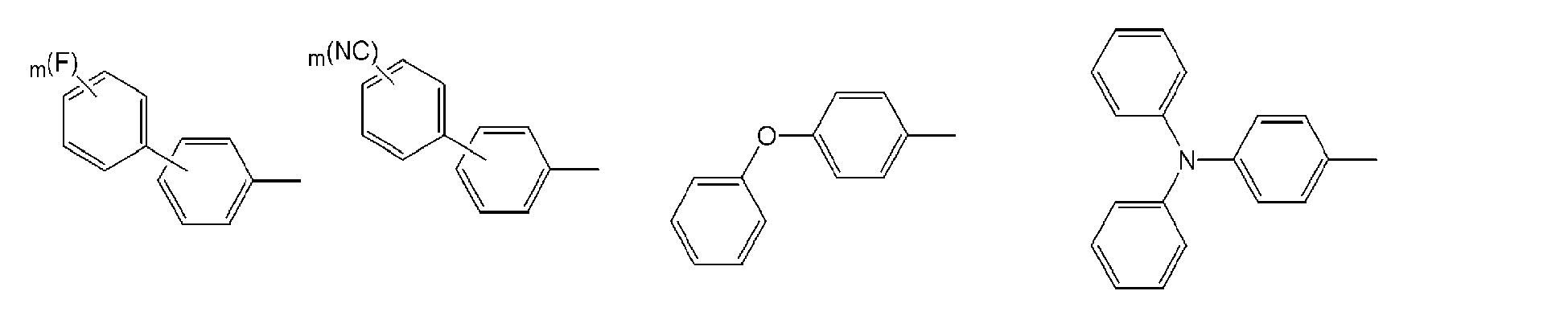


- The compound of any of the preceding claims, wherein R1, R2 and R3 are each independently selected from the group consisting of substituted or unsubstituted C1-C10 alkyl groups, substituted or unsubstituted C1-C10 alkoxy groups, substituted or unsubstituted C6-C12 aryl groups, substituted or unsubstituted C6-C12 aryloxy groups and substituted or unsubstituted C3-C12 heteroaryl groups.
- The compound of claim 10, wherein R1, R2 and R3 are each independently selected from the group consisting of C1-C10 alkyl groups, phenyl, halophenyl groups, cyanophenyl groups, C1-C10 alkylphenyl groups, C1-C10 alkoxyphenyl groups, biphenyl, halobiphenyl groups, naphthyl, halonaphthyl groups, C1-C10 alkylnaphthyl groups, and C1-C10 alkoxynaphthyl groups.
- The compound of claim 1, wherein the silanylamine-based compound is selected from the group consisting of Compounds 9, 43, 44, 45 and 137:


- A method of preparing a silanylamine-based compound represented by Formula (I) comprising reacting a compound represented by Formula 1a and a compound represented by Formula 1 b by Reaction Scheme 1:

n is an integer ranging from 0 to 5;
Ar1 and Ar2 are each independently selected from the group consisting of hydrogen, substituted or unsubstituted C6-C30 aryl groups, substituted or unsubstituted C2-C30 heteroaryl groups and
R1, R2 and R3 are each independently selected from the group consisting of hydrogen, substituted or unsubstituted C1-C30 alkyl groups, substituted or unsubstituted C2-C30 alkenyl groups, substituted or unsubstituted C2-C30 alkynyl groups, substituted or unsubstituted C1-C30 alkoxy groups, substituted or unsubstituted C6-C30 aryloxy groups, substituted or unsubstituted C6-C30 aryl groups and substituted or unsubstituted C2-C30 heteroaryl groups, wherein at least two of R1, R2 and R3 may be bonded to each other to form a saturated or unsaturated ring; and
Y is a halogen atom. - An organic light emitting device comprising:a first electrode;a second electrode; andan organic layer positioned between the first electrode and the second electrode, wherein the organic layer comprises the compound of Formula I according to any of claims 1 to 12.
- The organic light emitting device of claim 14, wherein the organic layer comprises one or more layers selected from the group consisting of hole injection layers, emissive layers, hole transport layers and electron transport layers and wherein the compound of Formula I is present in at least one of the hole injection layer, the hole transport layer or the emissive layer.
- Use of a compound according to Formula I of any of claims 1 to 12 as a hole injecting material for an organic light emitting device.
- Use of a compound according to Formula I of any of claims 1 to 12 as a hole transporting material for an organic light emitting device.
- Use of a compound according to Formula I of any of claims 1 to 12 as an emissive material for an organic light emitting device.
Applications Claiming Priority (1)
| Application Number | Priority Date | Filing Date | Title |
|---|---|---|---|
| KR1020060110187A KR100846590B1 (en) | 2006-11-08 | 2006-11-08 | Silaneyl amine-based compound, method for manufacturing the same, and an organic light emitting device having an organic film including the same |
Publications (2)
| Publication Number | Publication Date |
|---|---|
| EP1921082A1 true EP1921082A1 (en) | 2008-05-14 |
| EP1921082B1 EP1921082B1 (en) | 2010-04-14 |
Family
ID=38830356
Family Applications (1)
| Application Number | Title | Priority Date | Filing Date |
|---|---|---|---|
| EP07119446A Active EP1921082B1 (en) | 2006-11-08 | 2007-10-29 | Silanylamine-based compound, method of preparing the same and organic light emitting device including organic layer comprising the silanylamine-based compound |
Country Status (7)
| Country | Link |
|---|---|
| US (1) | US7927719B2 (en) |
| EP (1) | EP1921082B1 (en) |
| JP (1) | JP4620079B2 (en) |
| KR (1) | KR100846590B1 (en) |
| CN (1) | CN101177431B (en) |
| DE (1) | DE602007005900D1 (en) |
| TW (1) | TWI360551B (en) |
Cited By (2)
| Publication number | Priority date | Publication date | Assignee | Title |
|---|---|---|---|---|
| WO2013064814A1 (en) * | 2011-11-02 | 2013-05-10 | Cambridge Display Technology Limited | Light emitting composition and device |
| US9458182B2 (en) | 2009-01-07 | 2016-10-04 | Basf Se | Silyl- and heteroatom-substituted compounds selected from carbazoles, dibenzofurans, dibenzothiophenes and dibenzophospholes, and use thereof in organic electronics |
Families Citing this family (35)
| Publication number | Priority date | Publication date | Assignee | Title |
|---|---|---|---|---|
| KR20090089073A (en) * | 2008-02-18 | 2009-08-21 | 삼성모바일디스플레이주식회사 | Organic light emitting device having a silanyl amine compound and an organic film including the same |
| JP5551344B2 (en) * | 2008-05-23 | 2014-07-16 | ローム株式会社 | Organic EL device |
| KR100965044B1 (en) * | 2008-06-03 | 2010-06-21 | 주식회사 두산 | Novel silicon-based compound, preparation method thereof and organic light emitting device using the same |
| WO2010041872A2 (en) * | 2008-10-08 | 2010-04-15 | 주식회사 엘지화학 | Novel compound and organic electronic device using same |
| JP2010114070A (en) * | 2008-10-10 | 2010-05-20 | Canon Inc | White organic el element |
| JPWO2010052932A1 (en) * | 2008-11-07 | 2012-04-05 | 保土谷化学工業株式会社 | Compound having triphenylsilyl group and triarylamine structure and organic electroluminescence device |
| EP2416627B1 (en) * | 2009-03-31 | 2019-01-02 | Nippon Steel & Sumikin Chemical Co., Ltd. | Organic electroluminescent device |
| CN102422451A (en) * | 2009-05-12 | 2012-04-18 | E.I.内穆尔杜邦公司 | Organic electronic device with electron tunneling layer |
| WO2011051404A1 (en) * | 2009-10-28 | 2011-05-05 | Basf Se | Heteroleptic carbene complexes and use thereof in organic electronics |
| US9142792B2 (en) * | 2010-06-18 | 2015-09-22 | Basf Se | Organic electronic devices comprising a layer comprising at least one metal organic compound and at least one metal oxide |
| EP2588527B1 (en) * | 2010-07-02 | 2017-10-25 | Nissan Chemical Industries, Ltd. | Hole transport compositions and related devices and methods (i) |
| CN102031105A (en) * | 2010-11-16 | 2011-04-27 | 西安瑞联近代电子材料有限责任公司 | Bipolar phosphorescence host materials based on tetraphernl silicane substituted carbazoles and organic electroluminescent device |
| KR102021273B1 (en) * | 2011-05-27 | 2019-09-16 | 가부시키가이샤 한도오따이 에네루기 켄큐쇼 | Carbazole compound, light-emitting element, light-emitting device, electronic device, and lighting device |
| CN103172652A (en) * | 2011-12-22 | 2013-06-26 | 海洋王照明科技股份有限公司 | Tetraphenyl silicon containing organic semiconductor material and preparation method thereof and organic electroluminescent device |
| KR101952707B1 (en) | 2012-01-03 | 2019-06-03 | 삼성디스플레이 주식회사 | Novel compound and organic light emitting device containing same |
| CN103305211B (en) * | 2012-03-09 | 2016-01-13 | 海洋王照明科技股份有限公司 | Phosphorescent light body material and preparation method thereof and organic electroluminescence device |
| KR20140071897A (en) | 2012-11-26 | 2014-06-12 | 가부시키가이샤 한도오따이 에네루기 켄큐쇼 | Light-emitting element, light-emitting device, electronic device, and lighting device |
| CN103848858A (en) * | 2012-11-28 | 2014-06-11 | 海洋王照明科技股份有限公司 | Organic semiconductor material and preparation method thereof and electroluminescent device |
| JP6307689B2 (en) * | 2012-12-05 | 2018-04-11 | 三星ディスプレイ株式會社Samsung Display Co.,Ltd. | AMINE DERIVATIVE, ORGANIC LIGHT EMITTING MATERIAL AND ORGANIC ELECTROLUMINESCENT DEVICE USING THE SAME |
| JP6208424B2 (en) | 2012-12-05 | 2017-10-04 | 三星ディスプレイ株式會社Samsung Display Co.,Ltd. | Amine derivative having fluorine-substituted aryl group, organic EL material including the same, and organic EL device using the same |
| KR102083984B1 (en) | 2013-01-28 | 2020-04-16 | 삼성디스플레이 주식회사 | Silicon-based compound and Organic light emitting diode comprising the same |
| CN104017185A (en) * | 2013-02-28 | 2014-09-03 | 海洋王照明科技股份有限公司 | Polymer containing tetraphenyl silicane and triphenylamine unit as well as preparation method and application of polymer |
| CN103788088B (en) * | 2013-12-10 | 2015-08-12 | 京东方科技集团股份有限公司 | Containing indoles and Acridine derivatives, preparation method and application thereof, organic luminescent device |
| JP2015172001A (en) * | 2014-03-11 | 2015-10-01 | 三星ディスプレイ株式會社Samsung Display Co.,Ltd. | Silane compound and organic electroluminescence device |
| KR102230191B1 (en) | 2014-05-14 | 2021-03-22 | 삼성디스플레이 주식회사 | Organic light-emitting device |
| KR102278609B1 (en) * | 2014-05-14 | 2021-07-19 | 삼성디스플레이 주식회사 | Organic light-emitting device |
| KR102274570B1 (en) * | 2014-07-23 | 2021-07-07 | 삼성전자주식회사 | Condensed cyclic compound and organic light emitting device including the same |
| KR102426713B1 (en) | 2014-09-01 | 2022-07-29 | 삼성디스플레이 주식회사 | Amine-based compound and organic light emitting diode comprising the same |
| JP2016100364A (en) | 2014-11-18 | 2016-05-30 | 三星ディスプレイ株式會社Samsung Display Co.,Ltd. | Material for organic electroluminescence device and organic electroluminescence device using the same |
| KR102666512B1 (en) | 2016-09-22 | 2024-05-20 | 삼성디스플레이 주식회사 | Amine compound and organic electroluminescence device including the same |
| KR102765129B1 (en) | 2016-12-05 | 2025-02-12 | 삼성디스플레이 주식회사 | Amine compound and organic electroluminescence device including the same |
| KR102797542B1 (en) | 2019-02-13 | 2025-04-21 | 삼성디스플레이 주식회사 | Organic light emitting device |
| KR102791099B1 (en) * | 2019-08-27 | 2025-04-08 | 삼성디스플레이 주식회사 | Compound and organic light emitting device comprising same |
| KR102880377B1 (en) * | 2020-11-10 | 2025-11-05 | 삼성디스플레이 주식회사 | Light emitting diode and amine compound for the same |
| CN114213444A (en) * | 2021-12-10 | 2022-03-22 | 陕西维世诺新材料有限公司 | Tetraphenylsilane derivative and preparation method thereof |
Citations (6)
| Publication number | Priority date | Publication date | Assignee | Title |
|---|---|---|---|---|
| US2960517A (en) | 1959-06-03 | 1960-11-15 | Olin Mathieson | Secondary and tertiary aminophenyl silanes |
| JPH05323634A (en) * | 1992-05-26 | 1993-12-07 | Konica Corp | Electrophotographic sensitive body |
| DE10114970A1 (en) * | 2001-03-27 | 2002-10-17 | Wella Ag | New 1,2-diamino-4-azolyl-, -4-furyl-, -4-thienyl-, -4-phenyl- and -4-azinyl-benzene compounds and known analogues are used in oxidative colorants for keratin fibers, especially human hair |
| DE102004020046A1 (en) * | 2003-12-22 | 2005-07-28 | Sensient Imaging Technologies Gmbh | New tris(diarylaminoaryl)amine derivatives, used as hole transport substance or luminescent substance in organic electroluminescent or electrophotographic device, have triaryl-methyl- or -silyl-aryl substituent(s) |
| US20070207346A1 (en) | 2006-03-02 | 2007-09-06 | Canon Kabushiki Kaisha | Organic light-emitting device |
| US20070205715A1 (en) * | 2006-03-02 | 2007-09-06 | Canon Kabushiki Kaisha | Silyl compound, light emitting material, and organic light emitting device using the same |
Family Cites Families (13)
| Publication number | Priority date | Publication date | Assignee | Title |
|---|---|---|---|---|
| US4356429A (en) * | 1980-07-17 | 1982-10-26 | Eastman Kodak Company | Organic electroluminescent cell |
| TW558561B (en) * | 1997-07-22 | 2003-10-21 | Sumitomo Chemical Co | Hole transporting polymer and organic electroluminescence device using the same |
| JPH11329734A (en) | 1998-03-10 | 1999-11-30 | Mitsubishi Chemical Corp | Organic electroluminescent device |
| EP1009043A3 (en) * | 1998-12-09 | 2002-07-03 | Eastman Kodak Company | Electroluminescent device with polyphenyl hydrocarbon hole transport layer |
| US6465115B2 (en) * | 1998-12-09 | 2002-10-15 | Eastman Kodak Company | Electroluminescent device with anthracene derivatives hole transport layer |
| GB0230155D0 (en) * | 2002-12-24 | 2003-02-05 | Syngenta Participations Ag | Chemical compounds |
| KR100537621B1 (en) | 2004-02-02 | 2005-12-19 | 삼성에스디아이 주식회사 | Iridium compound and organic electroluminescent display device using the same |
| KR101154185B1 (en) * | 2004-06-15 | 2012-06-18 | 동우 화인켐 주식회사 | Organosilane Compounds, Materials Comprising Them, and Electroluminiscent Device Containing the Materials |
| JP4564790B2 (en) | 2004-06-28 | 2010-10-20 | 株式会社堀場製作所 | Pretreatment apparatus and method for gas analysis |
| GB0417036D0 (en) * | 2004-07-30 | 2004-09-01 | Avecia Ltd | Compounds, compositions and devices |
| JP2006056957A (en) | 2004-08-19 | 2006-03-02 | Nakamoto Pakkusu Kk | Apparatus for converting waste plastic into oil |
| KR100822212B1 (en) * | 2007-01-15 | 2008-04-16 | 삼성에스디아이 주식회사 | Organic light emitting device having a silanyl amine compound and an organic film including the same |
| KR20090089073A (en) * | 2008-02-18 | 2009-08-21 | 삼성모바일디스플레이주식회사 | Organic light emitting device having a silanyl amine compound and an organic film including the same |
-
2006
- 2006-11-08 KR KR1020060110187A patent/KR100846590B1/en not_active Expired - Fee Related
-
2007
- 2007-05-22 JP JP2007135428A patent/JP4620079B2/en active Active
- 2007-06-28 TW TW096123449A patent/TWI360551B/en not_active IP Right Cessation
- 2007-07-12 US US11/777,204 patent/US7927719B2/en active Active
- 2007-10-29 EP EP07119446A patent/EP1921082B1/en active Active
- 2007-10-29 DE DE602007005900T patent/DE602007005900D1/en active Active
- 2007-10-30 CN CN2007101848323A patent/CN101177431B/en active Active
Patent Citations (6)
| Publication number | Priority date | Publication date | Assignee | Title |
|---|---|---|---|---|
| US2960517A (en) | 1959-06-03 | 1960-11-15 | Olin Mathieson | Secondary and tertiary aminophenyl silanes |
| JPH05323634A (en) * | 1992-05-26 | 1993-12-07 | Konica Corp | Electrophotographic sensitive body |
| DE10114970A1 (en) * | 2001-03-27 | 2002-10-17 | Wella Ag | New 1,2-diamino-4-azolyl-, -4-furyl-, -4-thienyl-, -4-phenyl- and -4-azinyl-benzene compounds and known analogues are used in oxidative colorants for keratin fibers, especially human hair |
| DE102004020046A1 (en) * | 2003-12-22 | 2005-07-28 | Sensient Imaging Technologies Gmbh | New tris(diarylaminoaryl)amine derivatives, used as hole transport substance or luminescent substance in organic electroluminescent or electrophotographic device, have triaryl-methyl- or -silyl-aryl substituent(s) |
| US20070207346A1 (en) | 2006-03-02 | 2007-09-06 | Canon Kabushiki Kaisha | Organic light-emitting device |
| US20070205715A1 (en) * | 2006-03-02 | 2007-09-06 | Canon Kabushiki Kaisha | Silyl compound, light emitting material, and organic light emitting device using the same |
Non-Patent Citations (1)
| Title |
|---|
| DATABASE CA [online] CHEMICAL ABSTRACTS SERVICE, COLUMBUS, OHIO, US; HIROSE, HISAHIRO: "Electrophotographic photoreceptor", XP002463376, retrieved from STN Database accession no. 121:311851 * |
Cited By (3)
| Publication number | Priority date | Publication date | Assignee | Title |
|---|---|---|---|---|
| US9458182B2 (en) | 2009-01-07 | 2016-10-04 | Basf Se | Silyl- and heteroatom-substituted compounds selected from carbazoles, dibenzofurans, dibenzothiophenes and dibenzophospholes, and use thereof in organic electronics |
| WO2013064814A1 (en) * | 2011-11-02 | 2013-05-10 | Cambridge Display Technology Limited | Light emitting composition and device |
| GB2508567A (en) * | 2011-11-02 | 2014-06-04 | Cambridge Display Tech Ltd | Light emitting composition and device |
Also Published As
| Publication number | Publication date |
|---|---|
| TW200829596A (en) | 2008-07-16 |
| CN101177431A (en) | 2008-05-14 |
| JP2008120786A (en) | 2008-05-29 |
| KR100846590B1 (en) | 2008-07-16 |
| JP4620079B2 (en) | 2011-01-26 |
| CN101177431B (en) | 2012-05-23 |
| US20080106188A1 (en) | 2008-05-08 |
| US7927719B2 (en) | 2011-04-19 |
| KR20080041941A (en) | 2008-05-14 |
| DE602007005900D1 (en) | 2010-05-27 |
| EP1921082B1 (en) | 2010-04-14 |
| TWI360551B (en) | 2012-03-21 |
Similar Documents
| Publication | Publication Date | Title |
|---|---|---|
| EP1921082B1 (en) | Silanylamine-based compound, method of preparing the same and organic light emitting device including organic layer comprising the silanylamine-based compound | |
| EP1862524B1 (en) | Organic light emitting device and flat panel display device comprising the same | |
| EP1925618B1 (en) | Imidazopyridine-based compounds and organic light emitting diode including organic layer comprising the imidazopyridine-based compounds | |
| EP1661888B1 (en) | Phenylcarbazole-based compound and organic electroluminescent device employing the same | |
| EP2292604B1 (en) | Condensed-cyclic compound and organic light emitting diode having organic layer including the same | |
| EP2110373B1 (en) | Bipyridine-based compound and organic light emitting diode employing organic layer comprising the same | |
| KR101022649B1 (en) | Heterocyclic compound and organic electroluminescent device using same | |
| KR101256205B1 (en) | Organic light emitting compound and organic light emitting device comprising the same | |
| KR100903102B1 (en) | An imidazopyridine-based compound and an organic light emitting diode employing an organic layer comprising the same | |
| KR20090010763A (en) | An organic light emitting device having an aromatic compound and an organic film comprising the same | |
| KR20090059849A (en) | Aromatic heterocyclic compound, an organic light emitting device having an organic film comprising the same and a method of manufacturing the organic light emitting device | |
| EP2292601A1 (en) | Phenanthro[2,3-b]pyrroles and Phenanthro[3,2-b]pyrroles for organic light-emitting devices | |
| EP1970376B1 (en) | Imidazopyrimidine-based compound and organic light-emitting device employing organic layer including the same | |
| KR20100011289A (en) | An aromatic heterocyclic compound and an organic light emitting diode comprising an organic layer comprising the same | |
| US7754349B2 (en) | Silanylamine-based compound and organic light-emitting device including organic layer including the silanylamine-based compound | |
| JP5160046B2 (en) | Aminostyryl compound, method for producing the same, and organic light-emitting device including the same | |
| JP5318367B2 (en) | Dimethylenecyclohexane compound, method for producing the same, and organic light-emitting device including the same | |
| KR100898073B1 (en) | Quinoxaline ring-containing compound and organic light emitting device using the same | |
| KR101372850B1 (en) | Dimethylenecyclohexane compound, method for preparing the same and organic light emitting device comprising the same | |
| KR101156425B1 (en) | Dimethylenecyclohexane compound, method for preparing the same and organic light emitting device comprising the same | |
| KR100730178B1 (en) | Carbazole ring-containing silicon-based compound and organic light-emitting device having an organic film comprising the same |
Legal Events
| Date | Code | Title | Description |
|---|---|---|---|
| PUAI | Public reference made under article 153(3) epc to a published international application that has entered the european phase |
Free format text: ORIGINAL CODE: 0009012 |
|
| 17P | Request for examination filed |
Effective date: 20071029 |
|
| AK | Designated contracting states |
Kind code of ref document: A1 Designated state(s): AT BE BG CH CY CZ DE DK EE ES FI FR GB GR HU IE IS IT LI LT LU LV MC MT NL PL PT RO SE SI SK TR |
|
| AX | Request for extension of the european patent |
Extension state: AL BA HR MK RS |
|
| AKX | Designation fees paid |
Designated state(s): DE FR GB |
|
| RAP1 | Party data changed (applicant data changed or rights of an application transferred) |
Owner name: SAMSUNG MOBILE DISPLAY CO., LTD. |
|
| 17Q | First examination report despatched |
Effective date: 20090526 |
|
| GRAP | Despatch of communication of intention to grant a patent |
Free format text: ORIGINAL CODE: EPIDOSNIGR1 |
|
| GRAS | Grant fee paid |
Free format text: ORIGINAL CODE: EPIDOSNIGR3 |
|
| GRAA | (expected) grant |
Free format text: ORIGINAL CODE: 0009210 |
|
| AK | Designated contracting states |
Kind code of ref document: B1 Designated state(s): DE FR GB |
|
| REG | Reference to a national code |
Ref country code: GB Ref legal event code: FG4D |
|
| REF | Corresponds to: |
Ref document number: 602007005900 Country of ref document: DE Date of ref document: 20100527 Kind code of ref document: P |
|
| REG | Reference to a national code |
Ref country code: DE Ref legal event code: R096 Ref document number: 602007005900 Country of ref document: DE Effective date: 20100527 |
|
| PLBE | No opposition filed within time limit |
Free format text: ORIGINAL CODE: 0009261 |
|
| STAA | Information on the status of an ep patent application or granted ep patent |
Free format text: STATUS: NO OPPOSITION FILED WITHIN TIME LIMIT |
|
| 26N | No opposition filed |
Effective date: 20110117 |
|
| REG | Reference to a national code |
Ref country code: DE Ref legal event code: R097 Ref document number: 602007005900 Country of ref document: DE Effective date: 20110117 |
|
| REG | Reference to a national code |
Ref country code: DE Ref legal event code: R082 Ref document number: 602007005900 Country of ref document: DE Representative=s name: GULDE HENGELHAUPT ZIEBIG & SCHNEIDER, DE |
|
| REG | Reference to a national code |
Ref country code: DE Ref legal event code: R082 Ref document number: 602007005900 Country of ref document: DE Representative=s name: GULDE HENGELHAUPT ZIEBIG & SCHNEIDER, DE Effective date: 20120921 Ref country code: DE Ref legal event code: R081 Ref document number: 602007005900 Country of ref document: DE Owner name: SAMSUNG DISPLAY CO., LTD., KR Free format text: FORMER OWNER: SAMSUNG MOBILE DISPLAY CO. LTD., SUWON, KR Effective date: 20120921 Ref country code: DE Ref legal event code: R082 Ref document number: 602007005900 Country of ref document: DE Representative=s name: GULDE & PARTNER PATENT- UND RECHTSANWALTSKANZL, DE Effective date: 20120921 Ref country code: DE Ref legal event code: R081 Ref document number: 602007005900 Country of ref document: DE Owner name: SAMSUNG DISPLAY CO., LTD., YONGIN-CITY, KR Free format text: FORMER OWNER: SAMSUNG MOBILE DISPLAY CO. LTD., SUWON, GYEONGGI, KR Effective date: 20120921 |
|
| REG | Reference to a national code |
Ref country code: GB Ref legal event code: 732E Free format text: REGISTERED BETWEEN 20130110 AND 20130116 |
|
| REG | Reference to a national code |
Ref country code: FR Ref legal event code: TP Owner name: SAMSUNG MOBILE DISPLAY CO., LTD., KR Effective date: 20130220 |
|
| REG | Reference to a national code |
Ref country code: FR Ref legal event code: PLFP Year of fee payment: 9 |
|
| REG | Reference to a national code |
Ref country code: FR Ref legal event code: PLFP Year of fee payment: 10 |
|
| REG | Reference to a national code |
Ref country code: FR Ref legal event code: PLFP Year of fee payment: 11 |
|
| REG | Reference to a national code |
Ref country code: FR Ref legal event code: PLFP Year of fee payment: 12 |
|
| P01 | Opt-out of the competence of the unified patent court (upc) registered |
Effective date: 20230515 |
|
| PGFP | Annual fee paid to national office [announced via postgrant information from national office to epo] |
Ref country code: GB Payment date: 20240920 Year of fee payment: 18 |
|
| PGFP | Annual fee paid to national office [announced via postgrant information from national office to epo] |
Ref country code: FR Payment date: 20240925 Year of fee payment: 18 |
|
| PGFP | Annual fee paid to national office [announced via postgrant information from national office to epo] |
Ref country code: DE Payment date: 20240920 Year of fee payment: 18 |