EP1918986A2 - MOS Device resistant to ionizing radiatiion - Google Patents
MOS Device resistant to ionizing radiatiion Download PDFInfo
- Publication number
- EP1918986A2 EP1918986A2 EP07119878A EP07119878A EP1918986A2 EP 1918986 A2 EP1918986 A2 EP 1918986A2 EP 07119878 A EP07119878 A EP 07119878A EP 07119878 A EP07119878 A EP 07119878A EP 1918986 A2 EP1918986 A2 EP 1918986A2
- Authority
- EP
- European Patent Office
- Prior art keywords
- region
- semiconductor layer
- forming
- dielectric
- surface semiconductor
- Prior art date
- Legal status (The legal status is an assumption and is not a legal conclusion. Google has not performed a legal analysis and makes no representation as to the accuracy of the status listed.)
- Ceased
Links
Images


Classifications
-
- H—ELECTRICITY
- H10—SEMICONDUCTOR DEVICES; ELECTRIC SOLID-STATE DEVICES NOT OTHERWISE PROVIDED FOR
- H10D—INORGANIC ELECTRIC SEMICONDUCTOR DEVICES
- H10D30/00—Field-effect transistors [FET]
- H10D30/60—Insulated-gate field-effect transistors [IGFET]
- H10D30/64—Double-diffused metal-oxide semiconductor [DMOS] FETs
- H10D30/66—Vertical DMOS [VDMOS] FETs
-
- H—ELECTRICITY
- H10—SEMICONDUCTOR DEVICES; ELECTRIC SOLID-STATE DEVICES NOT OTHERWISE PROVIDED FOR
- H10D—INORGANIC ELECTRIC SEMICONDUCTOR DEVICES
- H10D30/00—Field-effect transistors [FET]
- H10D30/01—Manufacture or treatment
- H10D30/021—Manufacture or treatment of FETs having insulated gates [IGFET]
- H10D30/028—Manufacture or treatment of FETs having insulated gates [IGFET] of double-diffused metal oxide semiconductor [DMOS] FETs
- H10D30/0291—Manufacture or treatment of FETs having insulated gates [IGFET] of double-diffused metal oxide semiconductor [DMOS] FETs of vertical DMOS [VDMOS] FETs
-
- H—ELECTRICITY
- H10—SEMICONDUCTOR DEVICES; ELECTRIC SOLID-STATE DEVICES NOT OTHERWISE PROVIDED FOR
- H10D—INORGANIC ELECTRIC SEMICONDUCTOR DEVICES
- H10D62/00—Semiconductor bodies, or regions thereof, of devices having potential barriers
- H10D62/10—Shapes, relative sizes or dispositions of the regions of the semiconductor bodies; Shapes of the semiconductor bodies
- H10D62/13—Semiconductor regions connected to electrodes carrying current to be rectified, amplified or switched, e.g. source or drain regions
- H10D62/149—Source or drain regions of field-effect devices
- H10D62/151—Source or drain regions of field-effect devices of IGFETs
- H10D62/156—Drain regions of DMOS transistors
- H10D62/157—Impurity concentrations or distributions
-
- H—ELECTRICITY
- H10—SEMICONDUCTOR DEVICES; ELECTRIC SOLID-STATE DEVICES NOT OTHERWISE PROVIDED FOR
- H10D—INORGANIC ELECTRIC SEMICONDUCTOR DEVICES
- H10D64/00—Electrodes of devices having potential barriers
- H10D64/20—Electrodes characterised by their shapes, relative sizes or dispositions
- H10D64/27—Electrodes not carrying the current to be rectified, amplified, oscillated or switched, e.g. gates
- H10D64/311—Gate electrodes for field-effect devices
- H10D64/411—Gate electrodes for field-effect devices for FETs
- H10D64/511—Gate electrodes for field-effect devices for FETs for IGFETs
- H10D64/514—Gate electrodes for field-effect devices for FETs for IGFETs characterised by the insulating layers
- H10D64/516—Gate electrodes for field-effect devices for FETs for IGFETs characterised by the insulating layers the thicknesses being non-uniform
Definitions
- the present invention relates to a MOS device resistant to ionizing radiation, in particular to a power VDMOS (Vertical Double-Diffused Metal Oxide Semiconductor) device, to which the following description will make explicit reference without this implying any loss in generality.
- VDMOS Very Double-Diffused Metal Oxide Semiconductor
- discrete power semiconductor devices used in a space environment must intrinsically have a high reliability.
- these devices must be resistant to space ionizing radiation, such as electromagnetic radiation of extremely high energy and penetrative power (gamma rays), beams of protons or electrons with energies even much higher than one MeV, cosmic rays constituted by more or less heavy ions having energies even higher than one TeV, or secondary irradiation by electromagnetic beams or beams of particles generated within the same space systems due to interactions with the cosmic radiation.
- space ionizing radiation such as electromagnetic radiation of extremely high energy and penetrative power (gamma rays), beams of protons or electrons with energies even much higher than one MeV, cosmic rays constituted by more or less heavy ions having energies even higher than one TeV, or secondary irradiation by electromagnetic beams or beams of particles generated within the same space systems due to interactions with the cosmic radiation.
- the interaction between the above sources of radiation or particles and the semiconductor device during operation can trigger mechanisms of electrical
- the above mechanisms are accompanied by an equally harmful degradation (at least in part cumulative) of gate dielectric on the active channel, caused by a drain overcurrent occurring in a transient way due to the interaction between a heavy ion and the active area of the device in the OFF state.
- an anomalous and intense current of carriers moves in a surface portion of the drain region towards the gate dielectric, and is in part driven by the electrical field towards the channel of the device.
- a VDMOS device comprising in a known manner: a substrate 2 of semiconductor material; an epitaxial surface layer 3, also of semiconductor material, having the same type of conductivity (for example, of an N type) as the substrate 2 and overlying the same substrate 2; a plurality of cells formed in a surface portion of the epitaxial surface layer 3, each comprising a body well 6 having conductivity opposite to that of the epitaxial surface layer 3 (in the example, of a P type), and a source region 7, set within the body well 6, and having the same type of conductivity as the substrate 2; an insulated gate structure 8, constituted by a dielectric gate region 9, formed above the intercell region comprised between adjacent body wells 6 (a surface portion of which is known as neck region, designated by 10) and partially overlapping the body wells 6 and the source regions 7, and by a gate-electrode region 11, formed on the dielectric gate region 9; as is known, the substrate 2 has the function of drain for the VDMOS device 1.
- an insulated gate structure 8 constituted by a
- the interaction between a heavy ion and the active area of the device generates a flow of electrons (designated by e ) directed towards the substrate 2, and a corresponding flow of holes (designated by p ) directed towards the conduction channel of the device (designated by 12 and defined by the portion of the body wells 6 set directly underneath the insulated gate structure 8, and delimited by the junction between the source region 7 and the body well 6 on one side, and by the junction between the body well 6 and the neck region 10, on the other).
- the surface geometry in the active area has a considerable influence in defining the intensity of the electrical-field transverse component E t (i.e., the component directed orthogonally to the surface of the epitaxial surface layer 3).
- This component together with the electrical-field longitudinal component E l , determines the direction of the resultant electrical field E , which is directed as a whole towards the gate dielectric on the conduction channel 12.
- a current I directed towards the dielectric gate region 9, or also injected into it, is thus originated, which can entail a progressive charging of the dielectric.
- This phenomenon can be increased by the effect of current amplification due to the interaction between the charge generated by ionization by the ion and the electrical drain field, and also by triggering of surface conduction of the parasitic bipolar transistor formed by the source region 7, the body region 6, and the drain region (epitaxial surface layer 3).
- the aim of the present invention is to provide a MOS device that will enable a solution to the aforesaid problems and disadvantages, and in particular will have a higher resistance to ionizing radiation.
- MOS device resistant to ionizing radiation and a corresponding manufacturing process are thus provided, as defined in claim 1 and 11, respectively.
- a first aspect of the present invention envisages increasing the depth of the MOS device active area via the formation, between the substrate and the epitaxial surface layer, of a further epitaxial layer, having appropriate thickness and resistivity.
- an epitaxial sublayer 21 is set between a substrate 2 and an epitaxial surface layer 3 in which device cells are provided (each comprising, as illustrated previously, a body well 6 and a source region 7).
- the type of conductivity of the epitaxial sublayer 21 is the same as that of the epitaxial surface layer 3, and its thickness is comparable with that of the epitaxial surface layer 3 (for example, it is comprised between approximately one half and twice the thickness of the epitaxial surface layer).
- the values of thickness and, mainly, of resistivity of the epitaxial sublayer 21 are chosen so as to maximize the effect of ohmic drop during the ionization transient, when the epitaxial sublayer 21 is traversed by a dense flow of electrons, which are generated by the impact of a heavy ion and by dynamic amplification mechanisms (principally, the aforesaid pre-triggering of the parasitic bipolar transistor) and are forced by the electrical field towards the drain termination.
- the presence of the epitaxial sublayer 21 leads to a double advantage: on the one hand, the active region involved in the drain electrical field E widens downwards, and hence the drain electrical field E decreases at the surface during the ionization transient; on the other hand, the gain of the parasitic bipolar transistor in conditions of strong injection is reduced due to the widening of the effective drain region (collector of the parasitic transistor), with consequent reduction in the current density of surface holes flowing towards the source region 7 and the dielectric gate region 9 during the transient.
- the resistivity of the epitaxial sublayer 21 is generally comprised between 10% and 50% of the resistivity of the epitaxial surface layer 3. In one embodiment the resistivity of the epitaxial sublayer 21 does not exceed 50% of the resistivity of the epitaxial surface layer 3.
- a second aspect of the present invention which is independent of the first aspect described previously but which contributes therewith to increasing the MOS device resistance to ionizing radiation, envisages providing a thicker layer of gate dielectric, exclusively at the neck region 10.
- the dielectric gate region 9 comprises in this case: first portions 9a, set laterally above the source region 7, the conduction channel 12, and side portions of the neck region 10, and having a first thickness (for example, smaller than 100 nm); and a second portion 9b, joined to the first portions 9a, set centrally above just the neck region 10 (in particular, above a central portion thereof) and having a second thickness, greater than the first thickness (by approximately one order of magnitude, for example comprised between 100 nm and 1500 nm).
- the second portion 9b has a stripe conformation and extends longitudinally and substantially coaxially with respect to an overlying gate-electrode region 11 (which also has a stripe conformation).
- lateral surfaces of the second portion 9b that are connected to the first portions 9a can be orthogonal to the surface of the epitaxial surface layer 3, or else inclined with respect to the orthogonal direction, for example by an angle of 45°, according to the manufacturing process (as will be clarified hereinafter).
- the presence of a thicker region of intercell dielectric on the neck region 10 enables a reduction of the transverse component of the electrical field E t (in particular, between gate and drain) on the neck region 10. Furthermore, the same thick intercell region induces indirectly a distortion of the distribution of surface field, which is such as to "smooth" the field lines on the surface and to reduce the transverse electrical field (in particular, between gate and source) on the conduction channel 12. Furthermore, advantageously, thanks to the maintenance of a reduced dielectric thickness on the channel region 12, the problem associated to the degradation of tolerance to TID mechanism is strongly limited, at least as regards channel parameters, such as the gate-source threshold voltage (Vgs th ).
- Vgs th gate-source threshold voltage
- the lateral and vertical dimensions of the thick intercell dielectric stripe determine how much both the characteristics of breakdown of the MOS device 20 and the resistance to SEE of the same device are modified.
- the thickness of the second portion 9b of the dielectric gate region 9 is chosen so as not to lead to an excessive reduction in the breakdown voltage BVdss of the device; for example, this thickness is comprised between 100 nm and 1500 nm and is also a function of the technology used, the voltage class, and the required levels of tolerance to radiation.
- the width of the second portion 9b is chosen so as to maximize the "planarizing" effect on the surface drain electrical field: the second portion 9b approaches as much as possible the end of the conduction channel 12, but does not non-overlap with the same channel.
- the overlying gate-electrode region 11 which also has a stripe conformation
- the second portion 9b is, for example, 3.7 ⁇ m wide, thus leaving an adequate safety margin from the end of the conduction channel 12, of 0.5 ⁇ m on each side.
- the manufacturing process of the MOS device 20 envisages first providing a wafer of semiconductor material comprising a substrate 2, and then forming the epitaxial sublayer 21 by epitaxial growth starting from the substrate 2, and forming the epitaxial surface layer 3 by epitaxial growth starting from the epitaxial sublayer 21 ( Figure 5).
- the epitaxial growth steps are executed prior to any phototechnique or other surface process.
- formation of the edge termination, opening of the active area, and cleaning of the surface of the wafer are carried out in a known way and hence not described in detail herein.
- a first variant envisages dielectric formation via CVD.
- an optional step of growth of a thin film (not illustrated) of thermal oxide is first carried out before deposition of the thick gate dielectric, and then a CVD deposition of a thick dielectric layer 25 is carried out.
- the thick dielectric layer 25 can be SG (Silicon Glass) or preferably USG (Undoped Silicon Glass), with thicknesses of from 100 nm to 1500 nm, and the technique of deposition may be PECVD, LPCVD or APCVD; also possible is the use of dielectric multilayers.
- An (optional) thermal process of dielectric densification is then performed.
- a second variant envisages, instead, formation of the thick dielectric layer 25 via thermal growth of a dielectric film (silicon oxide, or a compound of oxynitride and silicon oxide) with a thickness of from 100 nm to 500 nm, above the epitaxial surface layer 3.
- a dielectric film silicon oxide, or a compound of oxynitride and silicon oxide
- the first variant is hence advantageous when it is necessary to provide large thicknesses of the dielectric stripe.
- an appropriate phototechnique is carried out for definition of the stripe of intercell-gate dielectric, having a longitudinal extension ( Figures 6a, 6b).
- a unidirectional dry etch, or an isotropic wet etch, of the thick dielectric layer 25 can be performed, so as to obtain the second portion 9b of the dielectric gate region 9 on the epitaxial surface layer 3.
- the dry etch leads to formation of side walls for the stripe that are orthogonal to the surface of the wafer, and is advantageous in markedly scaled devices, for containment of lateral dimensions.
- Wet etching is preferable when the spacing between contiguous cells is not excessively small, and the thickness of the stripe is not excessive (between approximately 100 nm and 200 nm).
- the final inclination of the side walls of the stripe is preferably approximately 45°. It is also possible to envisage a sequential wet/dry etch.
- a further step of cleaning of the surface of the wafer is then carried out, followed by the formation, by means of thermal oxidation, of a thin dielectric layer 26 ( Figure 7) laterally with respect to the stripe of gate dielectric.
- the dielectric can be, for example, oxynitride, or a multilayer of oxide, nitride, and oxide, with a thickness of less than 100 nm.
- a gate-electrode layer 27 is then deposited above the wafer of semiconductor material; the gate-electrode layer 27 is for example formed by doped polysilicon or by a double layer of doped polysilicon and metal silicide having a thickness of between 100 nm and 600 nm.
- a CVD deposition of a first dielectric layer made of USG, PSG, TEOS, or some other dielectric or dielectric multilayer, is carried out.
- a suitable phototechnique for defining the gate electrode 11 Figure 8
- a unidirectional etch of the first dielectric layer is first performed, with end-point on the gate-electrode layer 27, so as to form a first dielectric region 28, and then a unidirectional etch of the gate-electrode layer 27, for a given time or with end-point on the thin dielectric layer 26, is carried out.
- Figure 9 in a known way that is not described in detail, a first process of ion implantation and diffusion, for formation of the body wells 6, and then (by means of an appropriate masking) a second process of ion implantation and diffusion for formation of the source regions 7 within the body wells 6 are performed.
- the body wells 6 extend underneath the gate structure, but not underneath the second portion 9b of the dielectric gate region 9.
- the second dielectric layer 29 can be made of USG, PSG, TEOS, or some other dielectric or dielectric multilayer with low conformability, and its thickness depends directly on the planar geometry of the wafer.
- a unidirectional etch is performed of the second dielectric layer 29 to form spacers 30 at the sides of the gate structure, and hence of the first dielectric region 28 and of the gate-electrode region 11 ( Figure 10).
- the etch removes also part of the thin dielectric layer 26, exposing the underlying source regions 7, and defining the first portions 9a of the dielectric gate region 9.
- the process terminates with metallization of the front of the wafer, which leads to formation of a metal layer 32 ( Figure 11), constituted, for example, by an aluminium alloy, and with "patterning" of the same metal layer.
- a metal layer 32 Figure 11
- deposition and photolithography of the final passivation according to known techniques, and preparation and metallization of the back of the wafer (drain contact of the device).
- a second embodiment of the manufacturing process envisages provision of the lateral insulation of the source contacts (in particular from the gate electrode 11) not via spacers as described previously (so-called self-aligned technique), but via the use of a photolithographic technique.
- the dielectric can once again be USG, PSG, TEOS, or some other dielectric or dielectric multilayer.
- a photomasking is carried out for opening the contacts, and in particular a dry etch or composite (dry/wet) etch of the intermediate dielectric layer 33.
- the etch removes also part of the thin dielectric layer 26, exposing the underlying source regions 7 and defining the first portions 9a of the dielectric gate region 9 ( Figure 14).
- the MOS device 20 has a high resistance to ionizing radiation and to electrical/physical degradation resulting therefrom in so far as it meets the dual need of: reducing the current density of holes flowing towards the gate and source regions during the transient (by means of the epitaxial sublayer 21); and of reducing the transverse component of the electrical field E t between the gate and the drain on the neck region 10 and between the gate and the source on the conduction channel 12 (by means of the stripe of thick gate dielectric).
- the composite structure of the dielectric gate region 9 on the elementary cell leads to further advantages in the performance of the MOS device 20, apart from the reliability effects. Amongst these, the most evident is the reduction in the gate capacitance, which leads to a sensible increase in the switching rate of the MOS device 20.
- the geometrical parameters of the device can vary according to the required functions, the design technology, and the characteristics required of the device.
- the second portion 9b of the dielectric region 9 may even have a width equal to the width of the neck region 10, also in this case not overlapping with respect to the conduction channel 12.
- the MOS device of 20 FIG. 3 may be disposed on an integrated circuit (IC) such as a processor or memory, which may be disposed within a system such as a computer system.
- IC integrated circuit
Landscapes
- Insulated Gate Type Field-Effect Transistor (AREA)
- Thin Film Transistor (AREA)
Abstract
Description
- The present invention relates to a MOS device resistant to ionizing radiation, in particular to a power VDMOS (Vertical Double-Diffused Metal Oxide Semiconductor) device, to which the following description will make explicit reference without this implying any loss in generality.
- As is known, discrete power semiconductor devices used in a space environment, for example, in space systems such as orbital satellites or vehicles for space exploration, must intrinsically have a high reliability. In particular, these devices must be resistant to space ionizing radiation, such as electromagnetic radiation of extremely high energy and penetrative power (gamma rays), beams of protons or electrons with energies even much higher than one MeV, cosmic rays constituted by more or less heavy ions having energies even higher than one TeV, or secondary irradiation by electromagnetic beams or beams of particles generated within the same space systems due to interactions with the cosmic radiation. The interaction between the above sources of radiation or particles and the semiconductor device during operation can trigger mechanisms of electrical degradation (ionization) or physical degradation (lattice dislocation), which can evolve in a quasi-instantaneous or cumulative way up to thermal destruction of the device.
- In discrete power MOSFET devices, the mechanisms underlying the possible physical degradation or failure are basically of two types, known as:
- TID (Total Ionizing Dose), i.e., generation of electron-hole pairs within dielectric layers and consequent accumulation over time of trapped charge, prevalently holes, in active and passive layers of the device, with progressive degradation of its operating characteristics;
- SEE (Single-Event Effects), i.e., quasi-instantaneous triggering of mechanisms of localized energy overload, which can give rise to marked drifts of the drain local electrical field and to derating of the drain-source breakdown voltage (process defined as SEB, Single-Event Burnout), or even to extremely high transient flows of charge or overvoltage pulses through active dielectric layers, with consequent permanent dielectric rupture (process defined as SEGR, Single-Event Gate Rupture).
- The above mechanisms are accompanied by an equally harmful degradation (at least in part cumulative) of gate dielectric on the active channel, caused by a drain overcurrent occurring in a transient way due to the interaction between a heavy ion and the active area of the device in the OFF state. In time intervals of a few nanoseconds, an anomalous and intense current of carriers moves in a surface portion of the drain region towards the gate dielectric, and is in part driven by the electrical field towards the channel of the device.
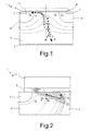
- In this regard, reference is made to Figure 1, showing a VDMOS device 1, comprising in a known manner: a
substrate 2 of semiconductor material; anepitaxial surface layer 3, also of semiconductor material, having the same type of conductivity (for example, of an N type) as thesubstrate 2 and overlying thesame substrate 2; a plurality of cells formed in a surface portion of theepitaxial surface layer 3, each comprising a body well 6 having conductivity opposite to that of the epitaxial surface layer 3 (in the example, of a P type), and asource region 7, set within the body well 6, and having the same type of conductivity as thesubstrate 2; aninsulated gate structure 8, constituted by adielectric gate region 9, formed above the intercell region comprised between adjacent body wells 6 (a surface portion of which is known as neck region, designated by 10) and partially overlapping thebody wells 6 and thesource regions 7, and by a gate-electrode region 11, formed on thedielectric gate region 9; as is known, thesubstrate 2 has the function of drain for the VDMOS device 1. - The interaction between a heavy ion and the active area of the device generates a flow of electrons (designated by e) directed towards the
substrate 2, and a corresponding flow of holes (designated by p) directed towards the conduction channel of the device (designated by 12 and defined by the portion of thebody wells 6 set directly underneath theinsulated gate structure 8, and delimited by the junction between thesource region 7 and the body well 6 on one side, and by the junction between the body well 6 and theneck region 10, on the other). As highlighted in the detail of Figure 2 (where field lines are represented with dashed lines), the surface geometry in the active area has a considerable influence in defining the intensity of the electrical-field transverse component Et (i.e., the component directed orthogonally to the surface of the epitaxial surface layer 3). This component, together with the electrical-field longitudinal component El, determines the direction of the resultant electrical fieldE , which is directed as a whole towards the gate dielectric on theconduction channel 12. A current I directed towards thedielectric gate region 9, or also injected into it, is thus originated, which can entail a progressive charging of the dielectric. This phenomenon can be increased by the effect of current amplification due to the interaction between the charge generated by ionization by the ion and the electrical drain field, and also by triggering of surface conduction of the parasitic bipolar transistor formed by thesource region 7, thebody region 6, and the drain region (epitaxial surface layer 3). - Typically, technological choices for reducing the incidence of SEGR or charge injection in the
dielectric gate region 9 involve the planar geometry of the active area or the thickness of thedielectric gate region 9. In particular, a uniform increase in the thickness of this region (typically constituted of silicon oxide) has proven effective in reducing the probability of SEGR both in theneck region 10 and in the channel region. In fact, the increase in thickness leads to a considerable reduction in the electrical-field transverse component Et, and thus in the injection/trapping of charge in the dielectric. At the same time, however, it has been found that thickening of the gate dielectric leads to a deterioration of the resistance to TID mechanism. Frequently, it is difficult to reach a compromise with TID tolerance, in particular in scaled devices, which must guarantee a low ON-resistance (Rdson). - The aim of the present invention is to provide a MOS device that will enable a solution to the aforesaid problems and disadvantages, and in particular will have a higher resistance to ionizing radiation.
- According to the present invention a MOS device resistant to ionizing radiation and a corresponding manufacturing process are thus provided, as defined in
claim 1 and 11, respectively. - For a better understanding of the present invention, preferred embodiments thereof are now described, purely by way of nonlimiting example, with reference to the attached drawings, wherein:
- Figure 1 shows a cross section of a MOS device of a known type;
- Figure 2 shows an enlarged detail of the cross section of Figure 1;
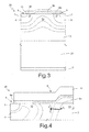
- Figure 3 shows a cross section of a MOS device, according to an aspect of the present invention;
- Figure 4 shows an enlarged detail of the cross section of Figure 3;
- Figure 5 shows a cross section through a wafer of semiconductor material in an initial step of a process for manufacturing a MOS device;
- Figure 6a is a top plan view of a portion of the wafer of Figure 5 in a subsequent step of the manufacturing process;
- Figure 6b is a cross section of the wafer of semiconductor material taken along the line VI-VI of Figure 6a;
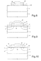
- Figures 7-11 show cross sections similar to that of Figure 6b in subsequent steps of the manufacturing process, according to a first embodiment of the present invention; and
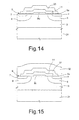
- Figures 12-15 show cross sections through a wafer of semiconductor material in subsequent steps of a process for manufacturing a MOS device, in accordance with a second embodiment of the present invention.
- As will be detailed hereinafter, a first aspect of the present invention envisages increasing the depth of the MOS device active area via the formation, between the substrate and the epitaxial surface layer, of a further epitaxial layer, having appropriate thickness and resistivity.
- In detail, and with reference to Figure 3 (where parts that are similar to others described previously are designated by the same reference numbers and will not be described again), in a
MOS device 20, in particular of a VDMOS type, made according to the present invention, anepitaxial sublayer 21 is set between asubstrate 2 and anepitaxial surface layer 3 in which device cells are provided (each comprising, as illustrated previously, a body well 6 and a source region 7). The type of conductivity of theepitaxial sublayer 21 is the same as that of theepitaxial surface layer 3, and its thickness is comparable with that of the epitaxial surface layer 3 (for example, it is comprised between approximately one half and twice the thickness of the epitaxial surface layer). Furthermore, the values of thickness and, mainly, of resistivity of theepitaxial sublayer 21 are chosen so as to maximize the effect of ohmic drop during the ionization transient, when theepitaxial sublayer 21 is traversed by a dense flow of electrons, which are generated by the impact of a heavy ion and by dynamic amplification mechanisms (principally, the aforesaid pre-triggering of the parasitic bipolar transistor) and are forced by the electrical field towards the drain termination. - The presence of the
epitaxial sublayer 21 leads to a double advantage: on the one hand, the active region involved in the drain electrical field E widens downwards, and hence the drain electrical field E decreases at the surface during the ionization transient; on the other hand, the gain of the parasitic bipolar transistor in conditions of strong injection is reduced due to the widening of the effective drain region (collector of the parasitic transistor), with consequent reduction in the current density of surface holes flowing towards thesource region 7 and thedielectric gate region 9 during the transient. The presence of the additional epitaxial layer can entail, however, a deterioration in the performance of theMOS device 20, basically as regards the ON-resistance (Rdson); for this reason, the resistivity of theepitaxial sublayer 21 is generally comprised between 10% and 50% of the resistivity of theepitaxial surface layer 3. In one embodiment the resistivity of theepitaxial sublayer 21 does not exceed 50% of the resistivity of theepitaxial surface layer 3. - A second aspect of the present invention, which is independent of the first aspect described previously but which contributes therewith to increasing the MOS device resistance to ionizing radiation, envisages providing a thicker layer of gate dielectric, exclusively at the
neck region 10. - In detail (see again Figure 3), the
dielectric gate region 9 comprises in this case:first portions 9a, set laterally above thesource region 7, theconduction channel 12, and side portions of theneck region 10, and having a first thickness (for example, smaller than 100 nm); and asecond portion 9b, joined to thefirst portions 9a, set centrally above just the neck region 10 (in particular, above a central portion thereof) and having a second thickness, greater than the first thickness (by approximately one order of magnitude, for example comprised between 100 nm and 1500 nm). Thesecond portion 9b has a stripe conformation and extends longitudinally and substantially coaxially with respect to an overlying gate-electrode region 11 (which also has a stripe conformation). Furthermore, lateral surfaces of thesecond portion 9b that are connected to thefirst portions 9a can be orthogonal to the surface of theepitaxial surface layer 3, or else inclined with respect to the orthogonal direction, for example by an angle of 45°, according to the manufacturing process (as will be clarified hereinafter). - As illustrated also in Figure 4, the presence of a thicker region of intercell dielectric on the
neck region 10 enables a reduction of the transverse component of the electrical field Et (in particular, between gate and drain) on theneck region 10. Furthermore, the same thick intercell region induces indirectly a distortion of the distribution of surface field, which is such as to "smooth" the field lines on the surface and to reduce the transverse electrical field (in particular, between gate and source) on theconduction channel 12. Furthermore, advantageously, thanks to the maintenance of a reduced dielectric thickness on thechannel region 12, the problem associated to the degradation of tolerance to TID mechanism is strongly limited, at least as regards channel parameters, such as the gate-source threshold voltage (Vgsth). - In greater detail, the lateral and vertical dimensions of the thick intercell dielectric stripe, as compared to the geometrical characteristics of the elementary cells and to the geometry and doping of the surface-drain and body regions, determine how much both the characteristics of breakdown of the
MOS device 20 and the resistance to SEE of the same device are modified. In particular, the thickness of thesecond portion 9b of thedielectric gate region 9 is chosen so as not to lead to an excessive reduction in the breakdown voltage BVdss of the device; for example, this thickness is comprised between 100 nm and 1500 nm and is also a function of the technology used, the voltage class, and the required levels of tolerance to radiation. The width of thesecond portion 9b is chosen so as to maximize the "planarizing" effect on the surface drain electrical field: thesecond portion 9b approaches as much as possible the end of theconduction channel 12, but does not non-overlap with the same channel. For example, if the overlying gate-electrode region 11 (which also has a stripe conformation) is 5.7 µm wide and the lateral diffusion of thebody wells 6 at the surface is 0.5 µm, thesecond portion 9b is, for example, 3.7 µm wide, thus leaving an adequate safety margin from the end of theconduction channel 12, of 0.5 µm on each side. - The manufacturing process of the
MOS device 20 envisages first providing a wafer of semiconductor material comprising asubstrate 2, and then forming theepitaxial sublayer 21 by epitaxial growth starting from thesubstrate 2, and forming theepitaxial surface layer 3 by epitaxial growth starting from the epitaxial sublayer 21 (Figure 5). In particular, the epitaxial growth steps are executed prior to any phototechnique or other surface process. Next, formation of the edge termination, opening of the active area, and cleaning of the surface of the wafer are carried out in a known way and hence not described in detail herein. - Next, the stripe of thick intercell dielectric is formed, according to two alternative variants.
- A first variant envisages dielectric formation via CVD. In detail, an optional step of growth of a thin film (not illustrated) of thermal oxide is first carried out before deposition of the thick gate dielectric, and then a CVD deposition of a thick
dielectric layer 25 is carried out. The thickdielectric layer 25 can be SG (Silicon Glass) or preferably USG (Undoped Silicon Glass), with thicknesses of from 100 nm to 1500 nm, and the technique of deposition may be PECVD, LPCVD or APCVD; also possible is the use of dielectric multilayers. An (optional) thermal process of dielectric densification is then performed. A second variant envisages, instead, formation of the thickdielectric layer 25 via thermal growth of a dielectric film (silicon oxide, or a compound of oxynitride and silicon oxide) with a thickness of from 100 nm to 500 nm, above theepitaxial surface layer 3. The first variant is hence advantageous when it is necessary to provide large thicknesses of the dielectric stripe. - After formation of the thick
dielectric layer 25, an appropriate phototechnique is carried out for definition of the stripe of intercell-gate dielectric, having a longitudinal extension (Figures 6a, 6b). In detail, a unidirectional dry etch, or an isotropic wet etch, of the thickdielectric layer 25 can be performed, so as to obtain thesecond portion 9b of thedielectric gate region 9 on theepitaxial surface layer 3. The dry etch leads to formation of side walls for the stripe that are orthogonal to the surface of the wafer, and is advantageous in markedly scaled devices, for containment of lateral dimensions. Wet etching is preferable when the spacing between contiguous cells is not excessively small, and the thickness of the stripe is not excessive (between approximately 100 nm and 200 nm). In this case, the final inclination of the side walls of the stripe is preferably approximately 45°. It is also possible to envisage a sequential wet/dry etch. - A further step of cleaning of the surface of the wafer is then carried out, followed by the formation, by means of thermal oxidation, of a thin dielectric layer 26 (Figure 7) laterally with respect to the stripe of gate dielectric. The dielectric can be, for example, oxynitride, or a multilayer of oxide, nitride, and oxide, with a thickness of less than 100 nm. A gate-
electrode layer 27 is then deposited above the wafer of semiconductor material; the gate-electrode layer 27 is for example formed by doped polysilicon or by a double layer of doped polysilicon and metal silicide having a thickness of between 100 nm and 600 nm. - At this point, according to a first embodiment of the manufacturing process, a CVD deposition of a first dielectric layer, made of USG, PSG, TEOS, or some other dielectric or dielectric multilayer, is carried out. This is followed by a suitable phototechnique for defining the gate electrode 11 (Figure 8). A unidirectional etch of the first dielectric layer is first performed, with end-point on the gate-
electrode layer 27, so as to form a firstdielectric region 28, and then a unidirectional etch of the gate-electrode layer 27, for a given time or with end-point on thethin dielectric layer 26, is carried out. - Next (Figure 9), in a known way that is not described in detail, a first process of ion implantation and diffusion, for formation of the
body wells 6, and then (by means of an appropriate masking) a second process of ion implantation and diffusion for formation of thesource regions 7 within thebody wells 6 are performed. In particular, after the diffusion, thebody wells 6 extend underneath the gate structure, but not underneath thesecond portion 9b of thedielectric gate region 9. - Then a CVD deposition is performed of a
second dielectric layer 29, which is to form spacers. Thesecond dielectric layer 29 can be made of USG, PSG, TEOS, or some other dielectric or dielectric multilayer with low conformability, and its thickness depends directly on the planar geometry of the wafer. - After a step of dielectric densification, a unidirectional etch is performed of the
second dielectric layer 29 to form spacers 30 at the sides of the gate structure, and hence of the firstdielectric region 28 and of the gate-electrode region 11 (Figure 10). The etch removes also part of thethin dielectric layer 26, exposing theunderlying source regions 7, and defining thefirst portions 9a of thedielectric gate region 9. - There follow optional steps, of a known type, of dry etching for a given time of silicon to form soft trenches, of metal deposition (Co, Pt, or other material) to form a metal silicide, followed by sintering of the film of contact silicide (having a thickness of 10÷ 100 nm) and by removal of the residual metal from the dielectric surfaces, and of deposition of a metallurgical barrier at the contact (Ti/TiN or the like). A photomasking is then carried out for opening gate contacts on pads, with a known technique.
- The process terminates with metallization of the front of the wafer, which leads to formation of a metal layer 32 (Figure 11), constituted, for example, by an aluminium alloy, and with "patterning" of the same metal layer. There follow deposition and photolithography of the final passivation, according to known techniques, and preparation and metallization of the back of the wafer (drain contact of the device).
- A second embodiment of the manufacturing process envisages provision of the lateral insulation of the source contacts (in particular from the gate electrode 11) not via spacers as described previously (so-called self-aligned technique), but via the use of a photolithographic technique.
- In detail, starting from the structure described in Figure 7 (after deposition of the gate-electrode layer 27), through an appropriate masking, a unidirectional etch of the gate-
electrode layer 27 is performed, for a given time or with end-point on the underlyingthin dielectric layer 26 to form the gate electrode 11 (Figure 12). - There follow processes of ion implantation and diffusion for formation of the
body wells 6 andsource regions 7, and CVD deposition of anintermediate dielectric layer 33 on thegate electrode 11 and the surface of the wafer (Figure 13). The dielectric can once again be USG, PSG, TEOS, or some other dielectric or dielectric multilayer. - After a step of dielectric densification, a photomasking is carried out for opening the contacts, and in particular a dry etch or composite (dry/wet) etch of the
intermediate dielectric layer 33. The etch removes also part of thethin dielectric layer 26, exposing theunderlying source regions 7 and defining thefirst portions 9a of the dielectric gate region 9 (Figure 14). - There follow the final steps described previously, and in particular metallization of the front for formation of the metal layer 32 (Figure 15).
- The advantages of the MOS device and the corresponding manufacturing process according to the invention are evident from the above.
- In particular, the
MOS device 20 has a high resistance to ionizing radiation and to electrical/physical degradation resulting therefrom in so far as it meets the dual need of: reducing the current density of holes flowing towards the gate and source regions during the transient (by means of the epitaxial sublayer 21); and of reducing the transverse component of the electrical field Et between the gate and the drain on theneck region 10 and between the gate and the source on the conduction channel 12 (by means of the stripe of thick gate dielectric). - Given the particular conformation of the
dielectric gate region 9, having a greater thickness only at the central stripe portion set above theneck region 10, it is also possible to reach a good compromise as regards resistance to the TID mechanism of theMOS device 20. - Furthermore, the composite structure of the
dielectric gate region 9 on the elementary cell leads to further advantages in the performance of theMOS device 20, apart from the reliability effects. Amongst these, the most evident is the reduction in the gate capacitance, which leads to a sensible increase in the switching rate of theMOS device 20. - Finally, it is clear that modifications and variations can be made to what is described and illustrated herein, without thereby departing from the scope of the present invention, as defined in the annexed claims.
- In particular, it is evident that what has been described and illustrated can be applied advantageously to power VDMOS devices having any type of edge-termination structure, and with the stripe in the active area having any dimension. The same teachings may be applied in other MOS devices, such as, for example, signal VDMOSs, IGBTs, and MOSFETs both of the N-channel and of the P-channel type. Furthermore, even though the entire description has been referred to the case of a P-channel VDMOS device, extension to the dual case of an N-channel VDMOS device is immediate.
- In addition, it is to be noted that the geometrical parameters of the device (for example, in terms of thickness and resistivity of the epitaxial layers, width of the stripe of gate dielectric, spacing between contiguous stripes, longitudinal pitch, and width/shape of the periodic contact cells) can vary according to the required functions, the design technology, and the characteristics required of the device. For example, the
second portion 9b of thedielectric region 9 may even have a width equal to the width of theneck region 10, also in this case not overlapping with respect to theconduction channel 12. - Finally, it is again emphasized that, even though the two aspects of the invention (presence of the
epitaxial sublayer 21 and of the thick dielectric stripe limitedly to the neck region 10) have been illustrated in combination and are jointly particularly advantageous (in so far as they enable a simultaneous solution to two main problems caused by ionizing radiation), they can possibly be implemented independently of one another. - The MOS device of 20 FIG. 3 (or a device having fewer than all of the attributes of the device 20) may be disposed on an integrated circuit (IC) such as a processor or memory, which may be disposed within a system such as a computer system.
Claims (23)
- A MOS device (20) resistant to ionizing radiation, comprising:- a surface semiconductor layer (3) having a first type of conductivity;- a gate structure (8) formed above said surface semiconductor layer (3), and having a dielectric gate region (9) and a gate-electrode region (11) overlying said dielectric gate region (9); and- body regions (6) having a second type of conductivity, formed within said surface semiconductor layer (3), laterally and partially underneath with respect to said gate structure (8),characterized in that said dielectric gate region (9) comprises a central region (9b) having a first thickness and side regions (9a) having a second thickness, smaller than said first thickness, said central region (9a) overlying an intercell region (10) of said surface semiconductor layer (3), set between said body regions (6).
- The device according to claim 1, further comprising a substrate (2) and a semiconductor sublayer (21), set between said substrate (2) and said surface semiconductor layer (3) underneath said surface semiconductor layer and having said first type of conductivity.
- The device according to claim 2, wherein said semiconductor sublayer (21) and said surface semiconductor layer (3) are epitaxial layers.
- The device according to claim 2 or 3, wherein said semiconductor sublayer (21) has a resistivity comprised between 10% and 50% of the resistivity of said surface semiconductor layer (3), and a thickness comprised between 50% and 200% of the thickness of said surface semiconductor layer (3) .
- The device according to any one of the preceding claims, wherein said central region (9a) and said side regions (9b) are joined continuously, and said central region (9b) has a width smaller than or equal to the width of said intercell region (10) .
- The device according to claim 5, further comprising source regions (7) having said first type of conductivity, formed within said body regions (6) and separated from said intercell region (10) by a respective channel region (12) of said MOS device (20); and wherein said side regions (9a) extend above said channel regions (12) and side portions of said intercell region (10), and said central region (9b) extends above a central portion of said intercell region (10).
- The device according to claim 5 or 6, wherein said central region (9b) has a thickness comprised between 100 nm and 1500 nm, and said side regions (9a) have a thickness smaller than 100 nm.
- The device according to any one of the preceding claims, wherein said central region (9b) has a stripe conformation and extends longitudinally above said intercell region (10).
- The device according to claim 8, wherein said central region (9b) has side walls inclined with respect to a direction orthogonal to the surface of said surface semiconductor layer (3), in particular by an angle of 45°.
- The device according to claim 8 or 9, wherein said gate-electrode region (11) also has a stripe conformation, and extends longitudinally and coaxially with respect to said central region (9b).
- The device according to any one of the preceding claims, for use in space environment applications.
- A process for manufacturing a MOS device (20) resistant to ionizing-radiation, comprising:- forming a surface semiconductor layer (3) having a first type of conductivity;- forming a gate structure (8) above said surface semiconductor layer (3), said step of forming a gate structure comprising forming a dielectric gate region (9) above said surface semiconductor layer (3) and forming a gate-electrode region (11) above said dielectric gate region (9); and- forming body regions (6) having a second type of conductivity within said surface semiconductor layer (3), laterally and partially underneath with respect to said gate structure (8);characterized in that forming said dielectric gate region (9) comprises forming a central region (9b) of said dielectric gate region, having a first thickness, above said surface semiconductor layer (3), and, subsequently, forming side regions (9a) of said dielectric gate region, having a second thickness, smaller than said first thickness.
- The process according to claim 12, further comprising providing a substrate (2), and forming a semiconductor sublayer (21), having said first type of conductivity, on said substrate; wherein said step of forming said surface semiconductor layer (2) comprises forming said surface semiconductor layer on said semiconductor sublayer (21).
- The process according to claim 13, wherein said step of forming a semiconductor sublayer (21) comprises epitaxial growth of said semiconductor sublayer starting from said substrate (2), and said step of forming a surface semiconductor layer (3) comprises epitaxial growth of said surface semiconductor layer starting from said semiconductor sublayer (21).
- The process according to claim 13 or 14, wherein said semiconductor sublayer (21) has a resistivity comprised between 10% and 50% of the resistivity of said surface semiconductor layer (3), and a thickness comprised between 50% and 200% of the thickness of said surface semiconductor layer (3).
- The process according to any one of claims 12-15, wherein forming said central region (9b) comprises depositing a layer of dielectric material (25) above said surface semiconductor layer (3).
- The process according to any one of claims 12-15, wherein forming said central region (9b) comprises thermal growth of a layer of dielectric material (25) on said surface semiconductor layer (3).
- The process according to claim 16 or 17, wherein forming said central region (9b) further comprises etching said layer of dielectric material (25) by means of a dry etch; or else by means of a wet etch so that said central region has side walls inclined with respect to a direction orthogonal to the surface of said surface semiconductor layer (3), in particular by an angle of 45°.
- The process according to claim 18, wherein said step of etching said layer of dielectric material (25) is such that said central region (9b) has a stripe conformation with longitudinal extension.
- The process according to any one of claims 12-19, wherein said step of forming side regions (9a) comprises, after said step of forming a central region (9b), forming a dielectric layer (26) above said surface semiconductor layer (3), joined continuously to said central region (9b); and wherein said central region (9b) has a thickness comprised between 100 nm and 1500 nm, and said dielectric layer (26) has a thickness smaller than 100 nm.
- The process according to claim 20, wherein said step of forming body regions (6) comprises introducing first dopant species in said surface semiconductor layer (3) so that said body regions (6) extend underneath said dielectric layer (26), but not underneath said central region (9b); said central region (9b) extending consequently above an intercell region (10) of said surface semiconductor layer (3), set between said body regions.
- The process according to claim 21, wherein said step of forming a gate-electrode region (11) comprises forming a layer of conductive material (27) above said central region (9b) and said dielectric layer (26), and subsequently etching said layer of conductive material (27) so that said gate-electrode region (11) extends on said central region (9b), longitudinally and coaxially thereto, and laterally with respect to said central region on said dielectric layer (26); said step of introducing first dopant species being subsequent to said step of forming a gate-electrode region (11).
- The process according to claim 21 or 22, further comprising introducing second dopant species in said body regions (6), for formation of source regions (7) having said first type of conductivity; wherein said step of forming side regions (9a) further comprises, subsequent to said step of introducing second dopant species, the step of etching said dielectric layer (26) so that said side regions (9a) extend above channel regions (12) of said MOS device (20), set between said source regions (7) and said intercell region (10), and side portions of said intercell region (10).
Applications Claiming Priority (1)
| Application Number | Priority Date | Filing Date | Title |
|---|---|---|---|
| IT000785A ITTO20060785A1 (en) | 2006-11-02 | 2006-11-02 | MOS DEVICE RESISTANT TO IONIZING RADIATION |
Publications (3)
| Publication Number | Publication Date |
|---|---|
| EP1918986A2 true EP1918986A2 (en) | 2008-05-07 |
| EP1918986A3 EP1918986A3 (en) | 2009-03-18 |
| EP1918986A9 EP1918986A9 (en) | 2009-05-13 |
Family
ID=38966711
Family Applications (1)
| Application Number | Title | Priority Date | Filing Date |
|---|---|---|---|
| EP07119878A Ceased EP1918986A3 (en) | 2006-11-02 | 2007-11-02 | MOS Device resistant to ionizing radiatiion |
Country Status (4)
| Country | Link |
|---|---|
| US (3) | US7791147B2 (en) |
| EP (1) | EP1918986A3 (en) |
| JP (1) | JP2008182191A (en) |
| IT (1) | ITTO20060785A1 (en) |
Cited By (5)
| Publication number | Priority date | Publication date | Assignee | Title |
|---|---|---|---|---|
| CN102544104A (en) * | 2012-01-12 | 2012-07-04 | 清华大学 | High-voltage resistant tunneling transistor and preparation method thereof |
| WO2014092936A1 (en) * | 2012-12-12 | 2014-06-19 | General Electric Company | Insulated gate field-effect transistor device and method of making the same |
| CN104600121A (en) * | 2015-01-15 | 2015-05-06 | 东南大学 | High-reliability P type silicon carbide vertical metal oxide semiconductor tube |
| CN104617144A (en) * | 2015-01-15 | 2015-05-13 | 东南大学 | High-reliability N type silicon carbide vertical metal oxide semiconductor pipe |
| CN109192659A (en) * | 2018-08-31 | 2019-01-11 | 江苏丽隽功率半导体有限公司 | A kind of production method of depletion field effect transistor |
Families Citing this family (14)
| Publication number | Priority date | Publication date | Assignee | Title |
|---|---|---|---|---|
| US20090159927A1 (en) * | 2007-12-21 | 2009-06-25 | Infineon Technologies Austria Ag | Integrated circuit device and method for its production |
| JP4935789B2 (en) * | 2008-10-06 | 2012-05-23 | トヨタ自動車株式会社 | Radiation irradiation test method for semiconductor devices |
| WO2010073991A1 (en) * | 2008-12-23 | 2010-07-01 | 三菱電機株式会社 | Semiconductor device and method for producing the same |
| US20100314695A1 (en) * | 2009-06-10 | 2010-12-16 | International Rectifier Corporation | Self-aligned vertical group III-V transistor and method for fabricated same |
| US8952458B2 (en) | 2011-04-14 | 2015-02-10 | Taiwan Semiconductor Manufacturing Company, Ltd. | Gate dielectric layer having interfacial layer and high-K dielectric over the interfacial layer |
| CN102339867A (en) * | 2011-10-28 | 2012-02-01 | 上海宏力半导体制造有限公司 | VDMOS (vertical-diffused metal oxide semiconductor) device and formation method thereof |
| CN104299944B (en) * | 2013-07-16 | 2018-07-10 | 中芯国际集成电路制造(上海)有限公司 | Flash memory and forming method thereof |
| CN104392932A (en) * | 2014-12-10 | 2015-03-04 | 中国电子科技集团公司第四十七研究所 | VDMOS (Vertical Diffused Metal Oxide Semiconductor) device and manufacturing method thereof |
| CN105870009A (en) * | 2015-01-21 | 2016-08-17 | 北大方正集团有限公司 | Power device manufacturing method and power device |
| US9842912B2 (en) | 2015-08-19 | 2017-12-12 | Fuji Electric Co., Ltd. | Semiconductor device and method of manufacturing semiconductor device |
| US10957791B2 (en) * | 2019-03-08 | 2021-03-23 | Infineon Technologies Americas Corp. | Power device with low gate charge and low figure of merit |
| CN112510080B (en) * | 2020-11-30 | 2023-06-06 | 西安微电子技术研究所 | Radiation-hardened structure and preparation method of a single-event-resistant high-voltage MOS field-effect transistor |
| CN114597251B (en) * | 2022-03-03 | 2023-05-26 | 电子科技大学 | Shielding grid VDMOS for resisting total dose radiation reinforcement |
| CN115832025A (en) * | 2022-11-21 | 2023-03-21 | 电子科技大学 | A SiC MOSFET structure with a second-stage oxide layer |
Citations (3)
| Publication number | Priority date | Publication date | Assignee | Title |
|---|---|---|---|---|
| US5674766A (en) | 1994-12-30 | 1997-10-07 | Siliconix Incorporated | Method of making a trench MOSFET with multi-resistivity drain to provide low on-resistance by varying dopant concentration in epitaxial layer |
| US6048759A (en) | 1998-02-11 | 2000-04-11 | Magepower Semiconductor Corporation | Gate/drain capacitance reduction for double gate-oxide DMOS without degrading avalanche breakdown |
| EP1503423A1 (en) * | 2003-07-31 | 2005-02-02 | STMicroelectronics S.r.l. | MIS power semiconductor device and method of making the same |
Family Cites Families (26)
| Publication number | Priority date | Publication date | Assignee | Title |
|---|---|---|---|---|
| US4974059A (en) * | 1982-12-21 | 1990-11-27 | International Rectifier Corporation | Semiconductor high-power mosfet device |
| US4587713A (en) * | 1984-02-22 | 1986-05-13 | Rca Corporation | Method for making vertical MOSFET with reduced bipolar effects |
| DE3851815T2 (en) | 1987-09-24 | 1995-05-24 | Mitsubishi Electric Corp | Field effect transistor and its manufacturing method. |
| US5355007A (en) * | 1990-11-23 | 1994-10-11 | Texas Instruments Incorporated | Devices for non-volatile memory, systems and methods |
| US5296393A (en) * | 1990-11-23 | 1994-03-22 | Texas Instruments Incorporated | Process for the simultaneous fabrication of high-and-low-voltage semiconductor devices, integrated circuit containing the same, systems and methods |
| US5204541A (en) * | 1991-06-28 | 1993-04-20 | Texas Instruments Incorporated | Gated thyristor and process for its simultaneous fabrication with high- and low-voltage semiconductor devices |
| US5273922A (en) | 1992-09-11 | 1993-12-28 | Motorola, Inc. | High speed, low gate/drain capacitance DMOS device |
| US5498554A (en) * | 1994-04-08 | 1996-03-12 | Texas Instruments Incorporated | Method of making extended drain resurf lateral DMOS devices |
| US5705835A (en) * | 1994-11-25 | 1998-01-06 | Fuji Electric Co., Ltd. | Semiconductor device and method of manufacturing the same |
| US5973367A (en) * | 1995-10-13 | 1999-10-26 | Siliconix Incorporated | Multiple gated MOSFET for use in DC-DC converter |
| US6084268A (en) * | 1996-03-05 | 2000-07-04 | Semiconductor Components Industries, Llc | Power MOSFET device having low on-resistance and method |
| US5973368A (en) * | 1996-06-05 | 1999-10-26 | Pearce; Lawrence G. | Monolithic class D amplifier |
| US6252278B1 (en) | 1998-05-18 | 2001-06-26 | Monolithic Power Systems, Inc. | Self-aligned lateral DMOS with spacer drift region |
| JP3602751B2 (en) | 1999-09-28 | 2004-12-15 | 株式会社東芝 | High voltage semiconductor device |
| US6407591B1 (en) * | 2000-06-30 | 2002-06-18 | Intel Corporation | Self-configurable clock input buffer compatible with high-voltage single-ended and low-voltage differential clock signals |
| KR100377130B1 (en) | 2000-11-22 | 2003-03-19 | 페어차일드코리아반도체 주식회사 | Semiconductor device and fabricating method thereof |
| US6486034B1 (en) | 2001-07-20 | 2002-11-26 | Taiwan Semiconductor Manufacturing Company | Method of forming LDMOS device with double N-layering |
| EP1421612B1 (en) | 2001-08-17 | 2009-04-22 | IHP GmbH-Innovations for High Performance Microelectronics/Institut für innovative Mikroelektronik | LDMOS Transistor and method of fabricating the same |
| US6734493B2 (en) * | 2002-02-08 | 2004-05-11 | Taiwan Semiconductor Manufacturing Co., Ltd. | Lateral double diffused metal oxide semiconductor (LDMOS) device with aligned buried layer isolation layer |
| KR100442881B1 (en) * | 2002-07-24 | 2004-08-02 | 삼성전자주식회사 | High voltage vertical double diffused MOS transistor and method for manufacturing the same |
| US20040164346A1 (en) * | 2003-02-20 | 2004-08-26 | Semiconductor Components Industries, Llc. | Power switching transistor with low drain to gate capacitance |
| US6900101B2 (en) * | 2003-06-13 | 2005-05-31 | Texas Instruments Incorporated | LDMOS transistors and methods for making the same |
| US6825531B1 (en) | 2003-07-11 | 2004-11-30 | Micrel, Incorporated | Lateral DMOS transistor with a self-aligned drain region |
| US7285822B2 (en) * | 2005-02-11 | 2007-10-23 | Alpha & Omega Semiconductor, Inc. | Power MOS device |
| DE102005042827A1 (en) | 2005-09-09 | 2007-03-22 | Atmel Germany Gmbh | High-voltage FET with source drain gate and channel has doped drift region having potential barrier spaced from the body region |
| JP5307973B2 (en) | 2006-02-24 | 2013-10-02 | セミコンダクター・コンポーネンツ・インダストリーズ・リミテッド・ライアビリティ・カンパニー | Semiconductor device |
-
2006
- 2006-11-02 IT IT000785A patent/ITTO20060785A1/en unknown
-
2007
- 2007-10-31 US US11/982,442 patent/US7791147B2/en active Active
- 2007-11-01 JP JP2007285476A patent/JP2008182191A/en not_active Withdrawn
- 2007-11-02 EP EP07119878A patent/EP1918986A3/en not_active Ceased
-
2010
- 2010-02-22 US US12/709,789 patent/US8471330B2/en active Active
- 2010-02-23 US US12/710,609 patent/US8187943B2/en active Active
Patent Citations (3)
| Publication number | Priority date | Publication date | Assignee | Title |
|---|---|---|---|---|
| US5674766A (en) | 1994-12-30 | 1997-10-07 | Siliconix Incorporated | Method of making a trench MOSFET with multi-resistivity drain to provide low on-resistance by varying dopant concentration in epitaxial layer |
| US6048759A (en) | 1998-02-11 | 2000-04-11 | Magepower Semiconductor Corporation | Gate/drain capacitance reduction for double gate-oxide DMOS without degrading avalanche breakdown |
| EP1503423A1 (en) * | 2003-07-31 | 2005-02-02 | STMicroelectronics S.r.l. | MIS power semiconductor device and method of making the same |
Non-Patent Citations (2)
| Title |
|---|
| MICKEVICIUS R V ET AL: "Simulation study of single-event gate rupture using radiation-hardened stripe cell power mosfet structures", IEEE TRANSACTIONS ON NUCLEAR SCIENCE, IEEE SERVICE CENTER, NEW YORK, NY, US, vol. 50, no. 6, 1 December 2003 (2003-12-01), pages 2256 - 2264, XP011106535, ISSN: 0018-9499, DOI: 10.1109/TNS.2003.821584 * |
| TITUS J L ET AL: "See characterization of vertical dmosfets: an updated test protocol", IEEE TRANSACTIONS ON NUCLEAR SCIENCE, IEEE SERVICE CENTER, NEW YORK, NY, US, vol. 50, no. 6, 1 December 2003 (2003-12-01), pages 2341 - 2351, XP011106549, ISSN: 0018-9499, DOI: 10.1109/TNS.2003.820733 * |
Cited By (8)
| Publication number | Priority date | Publication date | Assignee | Title |
|---|---|---|---|---|
| CN102544104A (en) * | 2012-01-12 | 2012-07-04 | 清华大学 | High-voltage resistant tunneling transistor and preparation method thereof |
| WO2014092936A1 (en) * | 2012-12-12 | 2014-06-19 | General Electric Company | Insulated gate field-effect transistor device and method of making the same |
| US9123798B2 (en) | 2012-12-12 | 2015-09-01 | General Electric Company | Insulating gate field effect transistor device and method for providing the same |
| EP4243080A3 (en) * | 2012-12-12 | 2023-11-08 | General Electric Company | Insulated gate field-effect transistor device and method of making the same |
| CN104600121A (en) * | 2015-01-15 | 2015-05-06 | 东南大学 | High-reliability P type silicon carbide vertical metal oxide semiconductor tube |
| CN104617144A (en) * | 2015-01-15 | 2015-05-13 | 东南大学 | High-reliability N type silicon carbide vertical metal oxide semiconductor pipe |
| CN109192659A (en) * | 2018-08-31 | 2019-01-11 | 江苏丽隽功率半导体有限公司 | A kind of production method of depletion field effect transistor |
| CN109192659B (en) * | 2018-08-31 | 2020-08-11 | 江苏丽隽功率半导体有限公司 | Manufacturing method of depletion type field effect transistor |
Also Published As
| Publication number | Publication date |
|---|---|
| US20100151647A1 (en) | 2010-06-17 |
| ITTO20060785A1 (en) | 2008-05-03 |
| US7791147B2 (en) | 2010-09-07 |
| US8471330B2 (en) | 2013-06-25 |
| US8187943B2 (en) | 2012-05-29 |
| US20080135928A1 (en) | 2008-06-12 |
| JP2008182191A (en) | 2008-08-07 |
| EP1918986A9 (en) | 2009-05-13 |
| US20110042739A1 (en) | 2011-02-24 |
| EP1918986A3 (en) | 2009-03-18 |
Similar Documents
| Publication | Publication Date | Title |
|---|---|---|
| US8471330B2 (en) | MOS device resistant to ionizing radiation | |
| US8692324B2 (en) | Semiconductor devices having charge balanced structure | |
| US7592228B2 (en) | Recessed clamping diode fabrication in trench devices | |
| US7777278B2 (en) | Lateral semiconductor component with a drift zone having at least one field electrode | |
| TWI500114B (en) | Semiconductor component and manufacturing method | |
| KR101254835B1 (en) | Trench-gate field effect transistors and methods of forming the same | |
| US7589378B2 (en) | Power LDMOS transistor | |
| US9099552B2 (en) | Semiconductor device and method of manufacturing the same | |
| US20190115436A1 (en) | Insulated gate semiconductor device having trench termination structure and method | |
| US20070267672A1 (en) | Semiconductor device and method for manufacturing same | |
| US20080017920A1 (en) | Structure and method for improving shielded gate field effect transistors | |
| US20100301411A1 (en) | Semiconductor device | |
| CN101107718A (en) | Power metal oxide semiconductor assembly | |
| US5132758A (en) | Semiconductor device and manufacturing method thereof | |
| KR100566599B1 (en) | Power MOSF with deep injection junction | |
| US11482616B2 (en) | Methods and structures for contacting shield conductor in a semiconductor device | |
| EP1761953A4 (en) | MOS SLUG TRANSISTOR COMPRISING A BLOCKING DIODE | |
| US10593793B2 (en) | Semiconductor device | |
| US20090026533A1 (en) | Trench MOSFET with multiple P-bodies for ruggedness and on-resistance improvements | |
| JP7721982B2 (en) | Semiconductor Devices | |
| US6255696B1 (en) | Retrograde ESD protection apparatus | |
| JP2023103365A (en) | semiconductor equipment | |
| TWI470796B (en) | Power ldmos transistor | |
| KR100868542B1 (en) | Trench MOOSFET with recessed clamping diode | |
| JPH0338748B2 (en) |
Legal Events
| Date | Code | Title | Description |
|---|---|---|---|
| PUAI | Public reference made under article 153(3) epc to a published international application that has entered the european phase |
Free format text: ORIGINAL CODE: 0009012 |
|
| AK | Designated contracting states |
Kind code of ref document: A2 Designated state(s): AT BE BG CH CY CZ DE DK EE ES FI FR GB GR HU IE IS IT LI LT LU LV MC MT NL PL PT RO SE SI SK TR |
|
| AX | Request for extension of the european patent |
Extension state: AL BA HR MK RS |
|
| RIN1 | Information on inventor provided before grant (corrected) |
Inventor name: CURRO', GIUSEPPE Inventor name: CASCIO, ALESSANDRA |
|
| PUAL | Search report despatched |
Free format text: ORIGINAL CODE: 0009013 |
|
| AK | Designated contracting states |
Kind code of ref document: A3 Designated state(s): AT BE BG CH CY CZ DE DK EE ES FI FR GB GR HU IE IS IT LI LT LU LV MC MT NL PL PT RO SE SI SK TR |
|
| AX | Request for extension of the european patent |
Extension state: AL BA HR MK RS |
|
| 17P | Request for examination filed |
Effective date: 20090318 |
|
| RTI1 | Title (correction) |
Free format text: MOS DEVICE RESISTANT TO IONIZING RADIATIION AND METHOD OF MANUFACTURING THE SAME |
|
| RTI1 | Title (correction) |
Free format text: MOS DEVICE RESISTANT TO IONIZING RADIATION AND METHOD OF MANUFACTURING THE SAME |
|
| 17Q | First examination report despatched |
Effective date: 20090513 |
|
| AKX | Designation fees paid |
Designated state(s): DE FR GB IT |
|
| RAP1 | Party data changed (applicant data changed or rights of an application transferred) |
Owner name: STMICROELECTRONICS SRL |
|
| RAP1 | Party data changed (applicant data changed or rights of an application transferred) |
Owner name: STMICROELECTRONICS SRL |
|
| STAA | Information on the status of an ep patent application or granted ep patent |
Free format text: STATUS: THE APPLICATION HAS BEEN REFUSED |
|
| 18R | Application refused |
Effective date: 20140620 |