EP1915037A1 - Bending-type rigid printed wiring board and process for producing the same - Google Patents
Bending-type rigid printed wiring board and process for producing the same Download PDFInfo
- Publication number
- EP1915037A1 EP1915037A1 EP06781905A EP06781905A EP1915037A1 EP 1915037 A1 EP1915037 A1 EP 1915037A1 EP 06781905 A EP06781905 A EP 06781905A EP 06781905 A EP06781905 A EP 06781905A EP 1915037 A1 EP1915037 A1 EP 1915037A1
- Authority
- EP
- European Patent Office
- Prior art keywords
- heat resistant
- resistant resin
- conductor
- wiring board
- printed wiring
- Prior art date
- Legal status (The legal status is an assumption and is not a legal conclusion. Google has not performed a legal analysis and makes no representation as to the accuracy of the status listed.)
- Granted
Links
Images









Classifications
-
- H—ELECTRICITY
- H05—ELECTRIC TECHNIQUES NOT OTHERWISE PROVIDED FOR
- H05K—PRINTED CIRCUITS; CASINGS OR CONSTRUCTIONAL DETAILS OF ELECTRIC APPARATUS; MANUFACTURE OF ASSEMBLAGES OF ELECTRICAL COMPONENTS
- H05K3/00—Apparatus or processes for manufacturing printed circuits
- H05K3/46—Manufacturing multilayer circuits
- H05K3/4688—Composite multilayer circuits, i.e. comprising insulating layers having different properties
- H05K3/4691—Rigid-flexible multilayer circuits comprising rigid and flexible layers, e.g. having in the bending regions only flexible layers
-
- H—ELECTRICITY
- H05—ELECTRIC TECHNIQUES NOT OTHERWISE PROVIDED FOR
- H05K—PRINTED CIRCUITS; CASINGS OR CONSTRUCTIONAL DETAILS OF ELECTRIC APPARATUS; MANUFACTURE OF ASSEMBLAGES OF ELECTRICAL COMPONENTS
- H05K1/00—Printed circuits
- H05K1/02—Details
-
- H—ELECTRICITY
- H05—ELECTRIC TECHNIQUES NOT OTHERWISE PROVIDED FOR
- H05K—PRINTED CIRCUITS; CASINGS OR CONSTRUCTIONAL DETAILS OF ELECTRIC APPARATUS; MANUFACTURE OF ASSEMBLAGES OF ELECTRICAL COMPONENTS
- H05K1/00—Printed circuits
- H05K1/02—Details
- H05K1/03—Use of materials for the substrate
- H05K1/0313—Organic insulating material
- H05K1/0353—Organic insulating material consisting of two or more materials, e.g. two or more polymers, polymer + filler, + reinforcement
- H05K1/036—Multilayers with layers of different types
-
- H—ELECTRICITY
- H05—ELECTRIC TECHNIQUES NOT OTHERWISE PROVIDED FOR
- H05K—PRINTED CIRCUITS; CASINGS OR CONSTRUCTIONAL DETAILS OF ELECTRIC APPARATUS; MANUFACTURE OF ASSEMBLAGES OF ELECTRICAL COMPONENTS
- H05K2201/00—Indexing scheme relating to printed circuits covered by H05K1/00
- H05K2201/01—Dielectrics
- H05K2201/0183—Dielectric layers
- H05K2201/0187—Dielectric layers with regions of different dielectrics in the same layer, e.g. in a printed capacitor for locally changing the dielectric properties
-
- H—ELECTRICITY
- H05—ELECTRIC TECHNIQUES NOT OTHERWISE PROVIDED FOR
- H05K—PRINTED CIRCUITS; CASINGS OR CONSTRUCTIONAL DETAILS OF ELECTRIC APPARATUS; MANUFACTURE OF ASSEMBLAGES OF ELECTRICAL COMPONENTS
- H05K2201/00—Indexing scheme relating to printed circuits covered by H05K1/00
- H05K2201/01—Dielectrics
- H05K2201/0183—Dielectric layers
- H05K2201/0195—Dielectric or adhesive layers comprising a plurality of layers, e.g. in a multilayer structure
-
- H—ELECTRICITY
- H05—ELECTRIC TECHNIQUES NOT OTHERWISE PROVIDED FOR
- H05K—PRINTED CIRCUITS; CASINGS OR CONSTRUCTIONAL DETAILS OF ELECTRIC APPARATUS; MANUFACTURE OF ASSEMBLAGES OF ELECTRICAL COMPONENTS
- H05K2201/00—Indexing scheme relating to printed circuits covered by H05K1/00
- H05K2201/10—Details of components or other objects attached to or integrated in a printed circuit board
- H05K2201/10227—Other objects, e.g. metallic pieces
- H05K2201/10295—Metallic connector elements partly mounted in a hole of the PCB
- H05K2201/10303—Pin-in-hole mounted pins
-
- H—ELECTRICITY
- H05—ELECTRIC TECHNIQUES NOT OTHERWISE PROVIDED FOR
- H05K—PRINTED CIRCUITS; CASINGS OR CONSTRUCTIONAL DETAILS OF ELECTRIC APPARATUS; MANUFACTURE OF ASSEMBLAGES OF ELECTRICAL COMPONENTS
- H05K2203/00—Indexing scheme relating to apparatus or processes for manufacturing printed circuits covered by H05K3/00
- H05K2203/30—Details of processes not otherwise provided for in H05K2203/01 - H05K2203/17
- H05K2203/308—Sacrificial means, e.g. for temporarily filling a space for making a via or a cavity or for making rigid-flexible PCBs
-
- H—ELECTRICITY
- H05—ELECTRIC TECHNIQUES NOT OTHERWISE PROVIDED FOR
- H05K—PRINTED CIRCUITS; CASINGS OR CONSTRUCTIONAL DETAILS OF ELECTRIC APPARATUS; MANUFACTURE OF ASSEMBLAGES OF ELECTRICAL COMPONENTS
- H05K3/00—Apparatus or processes for manufacturing printed circuits
- H05K3/46—Manufacturing multilayer circuits
- H05K3/4611—Manufacturing multilayer circuits by laminating two or more circuit boards
- H05K3/4626—Manufacturing multilayer circuits by laminating two or more circuit boards characterised by the insulating layers or materials
-
- H—ELECTRICITY
- H05—ELECTRIC TECHNIQUES NOT OTHERWISE PROVIDED FOR
- H05K—PRINTED CIRCUITS; CASINGS OR CONSTRUCTIONAL DETAILS OF ELECTRIC APPARATUS; MANUFACTURE OF ASSEMBLAGES OF ELECTRICAL COMPONENTS
- H05K3/00—Apparatus or processes for manufacturing printed circuits
- H05K3/46—Manufacturing multilayer circuits
- H05K3/4644—Manufacturing multilayer circuits by building the multilayer layer by layer, i.e. build-up multilayer circuits
- H05K3/4652—Adding a circuit layer by laminating a metal foil or a preformed metal foil pattern
-
- H—ELECTRICITY
- H05—ELECTRIC TECHNIQUES NOT OTHERWISE PROVIDED FOR
- H05K—PRINTED CIRCUITS; CASINGS OR CONSTRUCTIONAL DETAILS OF ELECTRIC APPARATUS; MANUFACTURE OF ASSEMBLAGES OF ELECTRICAL COMPONENTS
- H05K3/00—Apparatus or processes for manufacturing printed circuits
- H05K3/46—Manufacturing multilayer circuits
- H05K3/4644—Manufacturing multilayer circuits by building the multilayer layer by layer, i.e. build-up multilayer circuits
- H05K3/4652—Adding a circuit layer by laminating a metal foil or a preformed metal foil pattern
- H05K3/4655—Adding a circuit layer by laminating a metal foil or a preformed metal foil pattern by using a laminate characterized by the insulating layer
-
- Y—GENERAL TAGGING OF NEW TECHNOLOGICAL DEVELOPMENTS; GENERAL TAGGING OF CROSS-SECTIONAL TECHNOLOGIES SPANNING OVER SEVERAL SECTIONS OF THE IPC; TECHNICAL SUBJECTS COVERED BY FORMER USPC CROSS-REFERENCE ART COLLECTIONS [XRACs] AND DIGESTS
- Y10—TECHNICAL SUBJECTS COVERED BY FORMER USPC
- Y10T—TECHNICAL SUBJECTS COVERED BY FORMER US CLASSIFICATION
- Y10T29/00—Metal working
- Y10T29/49—Method of mechanical manufacture
- Y10T29/49002—Electrical device making
- Y10T29/49117—Conductor or circuit manufacturing
- Y10T29/49124—On flat or curved insulated base, e.g., printed circuit, etc.
-
- Y—GENERAL TAGGING OF NEW TECHNOLOGICAL DEVELOPMENTS; GENERAL TAGGING OF CROSS-SECTIONAL TECHNOLOGIES SPANNING OVER SEVERAL SECTIONS OF THE IPC; TECHNICAL SUBJECTS COVERED BY FORMER USPC CROSS-REFERENCE ART COLLECTIONS [XRACs] AND DIGESTS
- Y10—TECHNICAL SUBJECTS COVERED BY FORMER USPC
- Y10T—TECHNICAL SUBJECTS COVERED BY FORMER US CLASSIFICATION
- Y10T29/00—Metal working
- Y10T29/49—Method of mechanical manufacture
- Y10T29/49002—Electrical device making
- Y10T29/49117—Conductor or circuit manufacturing
- Y10T29/49124—On flat or curved insulated base, e.g., printed circuit, etc.
- Y10T29/49126—Assembling bases
-
- Y—GENERAL TAGGING OF NEW TECHNOLOGICAL DEVELOPMENTS; GENERAL TAGGING OF CROSS-SECTIONAL TECHNOLOGIES SPANNING OVER SEVERAL SECTIONS OF THE IPC; TECHNICAL SUBJECTS COVERED BY FORMER USPC CROSS-REFERENCE ART COLLECTIONS [XRACs] AND DIGESTS
- Y10—TECHNICAL SUBJECTS COVERED BY FORMER USPC
- Y10T—TECHNICAL SUBJECTS COVERED BY FORMER US CLASSIFICATION
- Y10T29/00—Metal working
- Y10T29/49—Method of mechanical manufacture
- Y10T29/49002—Electrical device making
- Y10T29/49117—Conductor or circuit manufacturing
- Y10T29/49124—On flat or curved insulated base, e.g., printed circuit, etc.
- Y10T29/49128—Assembling formed circuit to base
-
- Y—GENERAL TAGGING OF NEW TECHNOLOGICAL DEVELOPMENTS; GENERAL TAGGING OF CROSS-SECTIONAL TECHNOLOGIES SPANNING OVER SEVERAL SECTIONS OF THE IPC; TECHNICAL SUBJECTS COVERED BY FORMER USPC CROSS-REFERENCE ART COLLECTIONS [XRACs] AND DIGESTS
- Y10—TECHNICAL SUBJECTS COVERED BY FORMER USPC
- Y10T—TECHNICAL SUBJECTS COVERED BY FORMER US CLASSIFICATION
- Y10T29/00—Metal working
- Y10T29/49—Method of mechanical manufacture
- Y10T29/49002—Electrical device making
- Y10T29/49117—Conductor or circuit manufacturing
- Y10T29/49124—On flat or curved insulated base, e.g., printed circuit, etc.
- Y10T29/4913—Assembling to base an electrical component, e.g., capacitor, etc.
-
- Y—GENERAL TAGGING OF NEW TECHNOLOGICAL DEVELOPMENTS; GENERAL TAGGING OF CROSS-SECTIONAL TECHNOLOGIES SPANNING OVER SEVERAL SECTIONS OF THE IPC; TECHNICAL SUBJECTS COVERED BY FORMER USPC CROSS-REFERENCE ART COLLECTIONS [XRACs] AND DIGESTS
- Y10—TECHNICAL SUBJECTS COVERED BY FORMER USPC
- Y10T—TECHNICAL SUBJECTS COVERED BY FORMER US CLASSIFICATION
- Y10T29/00—Metal working
- Y10T29/49—Method of mechanical manufacture
- Y10T29/49002—Electrical device making
- Y10T29/49117—Conductor or circuit manufacturing
- Y10T29/49124—On flat or curved insulated base, e.g., printed circuit, etc.
- Y10T29/49155—Manufacturing circuit on or in base
-
- Y—GENERAL TAGGING OF NEW TECHNOLOGICAL DEVELOPMENTS; GENERAL TAGGING OF CROSS-SECTIONAL TECHNOLOGIES SPANNING OVER SEVERAL SECTIONS OF THE IPC; TECHNICAL SUBJECTS COVERED BY FORMER USPC CROSS-REFERENCE ART COLLECTIONS [XRACs] AND DIGESTS
- Y10—TECHNICAL SUBJECTS COVERED BY FORMER USPC
- Y10T—TECHNICAL SUBJECTS COVERED BY FORMER US CLASSIFICATION
- Y10T29/00—Metal working
- Y10T29/49—Method of mechanical manufacture
- Y10T29/49002—Electrical device making
- Y10T29/49117—Conductor or circuit manufacturing
- Y10T29/49124—On flat or curved insulated base, e.g., printed circuit, etc.
- Y10T29/49155—Manufacturing circuit on or in base
- Y10T29/49165—Manufacturing circuit on or in base by forming conductive walled aperture in base
Definitions
- the present invention relates to a printed wiring board which permits easy mounting of electrical parts and the like and which not only enables spaces to be saved, but also facilitates manufacturing.
- an electric connection box in which a rigid printed wiring board that is constructed in such a manner that a circuit is formed on the surface of a hard base material is used as a wiring material for distributing power from a power source (hereinafter referred to as an internal circuit).
- a method of manufacturing a rigid printed wiring board 100 by prior art will be described with reference to Figures 15 (a) to 15(c) .
- a laminate 103 which is obtained by laminating a conductor layer 102, such as copper foil and silver foil, each on a front surface and a rear surface of a hard base material 101 made of an insulating material, is used (refer to Figure 15(a) ), and through holes 104 (a via through hole 104a which ensures electrically conducting properties for the conductor layers 102 on the front and rear surfaces and a mounting through hole 104b for providing a connection terminal 20) are formed by planting a substrate through-hole provided by drilling the laminate 103.
- a circuit 102a is formed on the front and rear surfaces of the hard base material 101 (refer to Figure 15 (b) ), and the front surface of the circuit is coated with a resist (an insulating material) 105, whereby a rigid printed wiring board 100 is manufactured (refer to Figure 15(c) ). Also, a multilayer wiring board has been similarly manufactured by performing laminating and pressing.
- the mounting through hole 104b for the insertion of the connection terminal 20 is provided beforehand in a connector for the connection to the electrical part and a connection to the electrical part, such as a fuse and a relay. After the press fitting of the connection terminal 20 into the above-described mounting through hole 104b, the rigid printed wiring board 100 and the connection terminal 20 are connected together after going through the step of flow soldering or reflow soldering.
- connection terminal 20 in connecting the connection terminal 20 to the rigid printed wiring board 100 which is provided with the via through hole 104a for ensuring the conducting properties of the circuits formed on the front and rear surfaces of the substrate and the mounting through hole 104b into which the connection terminal 20 is press fitted, because the above-described mounting through hole 104b is formed from a hole which pierces through the substrate, in a case where a substrate circuit in which the connection terminals 20 are provided at prescribed positions each on the front surface and rear surface of the substrate, it is necessary to design a substrate circuit in such a manner that the positions of the connection terminals 20 do not overlap on the front and rear surfaces. Therefore, the prior part had the disadvantage that the projected area of the substrate circuit becomes large.
- connection terminals 20 are provided at prescribed positions each on the front surface and rear surface of the substrate. That is, it has been necessary to perform the soldering step twice.
- connection terminals 20 which are provided at prescribed positions on each of the front surfaces of the two rigid printed wiring boards 100 connected together by the electric wire 107 are soldered and fixed (refer to Figure 17 (a) ), and after that, the two rigid printed wiring boards 100 are bent in the above-described electric wire portion, whereby a substrate circuit in which the connection terminals are provided at prescribed positions on both surfaces is obtained (refer to Figure 17 (b) ). Therefore, it is necessary only that the soldering step for fixing the connection terminals 20 be performed once and besides the connection terminals 20 can be provided at arbitrary positions on both surfaces of the substrate.
- a bent portion obtained by partially reducing the thickness of the base material is provided so that the rigid printed wiring board can be bent in this bent portion.
- a circuit for large current for example, an inner circuit of an electric connection box
- a circuit for small current for example, an electronic circuit
- a heat resistant resin layer is laminated on a front surface of a hard core material provided so as to contain a gap portion and also on a top surface of the gap portion, a heat resistant resin layer is laminated on a rear surface of the core material except the gap portion, a conductor layer is laminated and firmly fixed via the heat resistant resin layers, and the conductor layer is etched, whereby a circuit is formed.
- Conductor portions having different layer thicknesses are formed on the same surface of the conductor, whereby a circuit for large current and a circuit for small current are formed on the same substrate.
- a method of manufacturing a bending rigid printed wiring board of the present invention comprises a step of burying a heat resistant resin material in a gap portion provided in a hard core material, a step of forming a laminate by laminating a conductor layer each on a front surface and a rear surface of the hard core material via heat resistant resin layers and performing hot pressing, a step of forming a circuit on the front surface and rear surface of the hard base material by etching the laminate and of removing the conductor layer on the rear surface of the gap portion of the hard core material, and a step of removing the heat resistant resin material buried in the gap portion along with the heat resistant resin material on the rear surface of the heat resistant resin material, whereby a bent portion obtained by partially reducing the thickness of the hard base material is formed.
- a rigid printed wiring board capable of being bent in the bent portion is obtained by performing the steps.
- a bending rigid printed wiring board of the present invention by providing a bent portion obtained by partially reducing the thickness of the hard base material, it is possible to bend the printed wiring board in the bent portion.
- a wiring material (a substrate circuit) of an internal circuit as used in electrical equipment is formed, after the provision of connection terminals at prescribed positions on a front surface of the rigid printed wiring board, the rigid printed wiring board is bent in the above-described bent portion, whereby it is possible to obtain a substrate circuit in which the connection terminals are provided on both surfaces. Therefore, the installation positions of the connection terminals can be arbitrarily designed and the soldering step of the connection terminals is performed only once.
- one rigid printed wiring board is bent in a bent portion obtained by partially reducing the thickness of a hard base material and, therefore, it is unnecessary to install electric wires for connecting together the circuits of opposed substrate surfaces.
- a gap portion is formed beforehand in part of the hard core material and a heat resistant resin material is buried in this gap portion.
- a laminate which is obtained by laminating a conductor layer on the front surface and rear surface of the hard core material via a heat resistant resin layer is used, and a heat resistant resin material buried in the gap portion is removed from the above-described laminate, whereby it is possible to easily form a bent portion which is obtained by partially reducing the thickness of the hard base material.
- the bending rigid printed wiring board is simple in construction and can be manufactured at low cost. Moreover, in manufacturing the bending rigid printed wiring board, conductor portions having different layer thicknesses are formed on the same surface of the conductor layer and a circuit for large current (for example, an inner circuit of an electric connection box) and a circuit for small current (for example, an electronic circuit) are formed, whereby it is possible to improve the substrate performance.
- a circuit for large current for example, an inner circuit of an electric connection box
- a circuit for small current for example, an electronic circuit
- a bending rigid printed wiring board and a method of manufacturing the bending rigid printed wiring board in embodiments of the present invention will be described with reference to Figure 1 to Figures 15(a) to 15(c) .
- the bending rigid printed wiring board 10 of this embodiment is such that in a bending rigid printed wiring board 10 in which an arbitrary circuit 14 is formed by etching a laminate 6 which is obtained by laminating a conductor layer 4 each on the front surface and rear surface of a hard base material 5, a bent portion 10A which is obtained by partially reducing the thickness of the above-described hard base material 5 is formed.
- a hard core material 1 from which a portion corresponding to the bent portion has been removed is used and a heat resistant resin material 2 is buried in a relevant gap portion (the portion from which the hard core material has been removed) 1A.
- a conductor layer 4 is laminated each on the front surface and rear surface of the hard core material 1, in which the heat resistant resin material 2 is buried in the gap portion 1A, via heat resistant resin layers 31, 32, and after that, hot pressing is performed, whereby the laminate 6 in which the conductor layer 4 is laminated each on both surfaces of the hard base material 5 is fabricated.
- a hard core material 1 formed from a glass epoxy resin is used.
- a gap portion 1A which is obtained by removing part of the core material in groove form, whereby the gap portion 1A was formed in a place corresponding to the bent portion (refer to Figure 1(a) ).
- a heat resistant resin material 2 such as a Teflon (registered trademark) sheet having a film thickness of 0.4 mm and silicone rubber, is buried in the above-described gap portion 1A, whereby the hard core material 1 in which the heat resistant resin material 2 is buried at a position corresponding to the bent portion is fabricated (refer to Figure 1 (b) ).
- a heat resistant resin material 2 such as a Teflon (registered trademark) sheet having a film thickness of 0.4 mm and silicone rubber
- a copper layer 4 having a film thickness of 200 ⁇ m to 600 ⁇ m is laminated (refer to Figure 1 (c) ) each on the front surface and rear surface of the above-described hard core material 1 via heat resistant resin layers 31, 32 having a film thickness of 0.1 mm (corresponding to adhesive layers for bonding the copper layer 4) and hot pressing is performed, whereby the laminate 6 in which the copper layer 4 is bonded to both surfaces of the hard base material 5 is fabricated(refer to Figure 1(d) ).
- a bonding sheet 31 having a layer thickness of 0.1 mm and a glass epoxy resin sheet (a prepreg) 32 having a layer thickness of 0.1 mm were used as the heat resistant resin layers 31, 32.
- the copper layer 4 was laminated on the front surface of the hard core material 1 in which the heat resistant resin material 2 is buried in the gap portion 1A via the bonding sheet 31 and, at the same time, the copper layer 4 was laminated on the rear surface of the hard core material 1 via the glass epoxy resin sheet (the prepreg) 32 and hot pressed, whereby the laminate 6 in which the copper layer 4 is bonded to both surfaces of the hard base material 5 was fabricated.
- the heat resistant resin layers 31, 32 (bonding sheets or glass epoxy resin sheets (prepregs)) cure thermally and the heat resistant resin layers 31, 32 become bonded to (become integral with) the hard core material 1, whereby the hard base material 5 having a layer thickness of 0. 6 mm is formed and, at the same time, the copper layer 4 becomes bonded via the heat resistant resin layers 31, 32, with the result that it is possible to obtain the laminate 6 in which the copper layer 4 is bonded to both surfaces of the hard base material 5.
- a glass epoxy resin sheet (a prepreg) is laminated on the hard core material 1 formed from a glass epoxy resin and hot pressing is performed, the hard core material 1 and the glass epoxy resin sheet (the prepreg) become integral with each other.
- the groove-shaped gap portion 1A was formed by removing part of the core material 1, the heat resistant resin material 2 was buried in this gap portion 1A, and the heat resistant resin layers 31, 32 were laminated on the front surface and rear surface of the core material.
- a heat resistant resin layer 32' in which a notch 32A similar to the above-described gap portion 1A is made, on the rear surface of the core material 1 in which the heat resistant resin material 2 is buried in the gap portion 1A and to laminate the copper layer 4 via the heat resistant resin 32' (refer to Figures 4(a) to 4(d) ).
- FIGS 3 (a) to 3(d) which illustrate the manufacturing process of a rigid printed wiring board
- arbitrary circuits 14 are formed on the front surface and rear surface of the hard base material 5 by etching the laminate 6 and the through hole 7 (the via through hole 7a which ensures the conducting properties of the circuits formed on the front surface and rear surface of the substrate and the mounting through hole 7b for providing the connection terminals at prescribed positions) is formed.
- the heat resistant resin material 2 buried in the gap portion 1A of the hard core material 1 is removed along with the heat resistant resin layer 32 laminated on the rear surface of the heat resistant resinmaterial 2, whereby the bent portion 10A obtained by reducing the thickness of the hard base material 5 in part is formed.
- the copper layer 4 at a position corresponding to the gap portion 1A of the hard core material 1 (on the rear surface of the heat resistant resin material 2) is removed by etching beforehand (an exposed portion 8).
- the heat resistant resin layer 32 was cut in the above-described exposed portion 8 and removed along with the heat resistant resin material 2 buried in the gap portion 1A, whereby the bent portion 10A obtained by partially reducing the thickness of the hard base material 5 was formed (refer to Figure 3(d) ). That is, by removing the heat resistant resin material 2 buried in the gap portion 1A along with the heat resistant resin layer 32 on the rear surface, a thin-walled portion consisting of the heat resistant resin layer 31 (bonding sheet) having a film thickness of 0.1 mm, which is a single layer, is formed in part of the hard base material 5 and the rigid printed wiring board can be bent in this thin-walled portion (the bent portion 10A).
- the circuit 14 made by etching the copper layer 4 having a layer thickness of 200 ⁇ m to 600 ⁇ m and it is ensured that circuits formed on the front surface of the hard base material 5 are connected together, the hard base material being arranged right and left, with the bent portion 10A interposed.
- a description will be given of a method of manufacturing a bending rigid printed wiring board 10 which involves laminating a conductor layer 4 on the front surface of a hard core material 1 in which a heat resistant resin material 2 is buried in a gap portion 1A via a heat resistant resin layer 31, at the same time laminating a conductor layer 4 on the rear surface of the hard core material 1 via a heat resistant resin layer 32' in which a notch 32A similar to the above-described gap portion 1A is made, performing hot pressing, whereby a laminate 61 in which the conductor layers 4 are bonded to both surfaces of the hard base material 51 is fabricated, and removing the heat resistant resin material 2 buried in the gap portion 1A from this laminate 61.
- a heat resistant resin material 2 such as a Teflon (registered trademark) sheet having a film thickness of 0.5 mm and silicone rubber, was buried in the gap portion 1A of the hard core material 1, and a convex portion having a height of 0.1 mm was formed, the convex portion being such that the heat resistant resin material 2 protrudes from the rear surface of the gap portion 1A.
- the notch 32A corresponding to the above-described convex portion was formed in the heat resistant resin layer 32' laminated on the rear surface of the hard core material 1, and the copper layer 4 having a layer thickness of 200 to 600 ⁇ m was laminated each on the front surface and rear surface of the hard core material 1, in which the heat resistant resin material 2 is buried in the gap portion 1A, via the heat resistant resin layers 31, 32' (refer to Figure 4(a) ).
- the copper layer 4 is laminated, via the heat resistant resin layer 31, on the front surface of the hard core material 1, in which the heat resistant resin material 2 is buried in the gap portion 1A, the copper layer 4 is laminated on the rear surface via the heat resistant resin layer 32' in which the notch 32A is made, and hot pressing is performed, the above-described heat resistant resin layers 31, 32' cure thermally and become bonded to (become integral with) the hard core material 1 and the hard base material 51 having a layer thickness of 0.6 mm is formed and, at the same time, the copper layer 4 becomes bonded via the above-described heat resistant resin layers 31, 32' , whereby it is possible to obtain the laminate 61 in which the copper layer 4 is laminated on both surfaces of the hard base material 51.
- the copper layer 4 is laminated on the rear surface of the heat resistant resin material 2 buried in the gap portion 1A without the interposition of the heat resistant resin layer 32'.
- arbitrary circuits 14 are formed on the front surface and rear surface of the hard base material 51 by etching the laminate 61 and at the same time, a through hole 7 (a via through hole 7a which ensures the conducting properties of the circuits formed on the front surface and rear surface of the substrate and a mounting through hole 7b for providing connection terminals at prescribed positions) is formed.
- the copper layer 4 on the rear surface of the heat resistant resin material 2 buried in the gap portion 1A is removed by etching beforehand (an exposed portion 8) .
- a bending rigid printed wiring board 10 provided with a bent portion 10A which is obtained by partially reducing the thickness of the hard base material 51 has been described above.
- the bending rigid printed wiring board is not limited to the both-side wiring board.
- a laminate 62 which is obtained by laminating, via a heat resistant resin layer 3, a conductor layer 4 on the front surface (a single side) of a hard core material 1, in which a heat resistant resin material 2 is buried in a gap portion 1A, is used (refer to Figure 5(a) ), and, by etching the laminate, circuits 14 are formed on the front surface of the hard base material 52 constituted by the hard core material 1 and the heat resistant resin layer 3 (refer to Figure 5(b) ).
- the heat resistant resin material 2 buried in the gap portion 1A of the hard core material 1 is removed and a thin-walled portion constituted by only a heat resistant resin layer 3, which is a single layer, is provided in part of the hard base material 52, whereby it is possible to obtain a bending rigid printed wiring board (a single-side wiring board) having a bent portion 10A formed by partially reducing the thickness of the hard base material 52 (refer to Figure 5(c) ).
- a hard core material 1 is laminated, via a heat resistant resin layer 31, on the front surface of a rigid wiring board in which circuits 14 are formed on the front surface of a hard core material 1 and hot pressing is performed, whereby a hard core material 11 in the form of a shielded plate is fabricated (refer to Figure 6(a) ), a gap portion 1A is formed by removing part of the hard core material 11 in the form of a shielded plate (refer to Figure 6(b) ), a conductor layer 4 is laminated, via a heat resistant resin layer 31, on the front surface of the core material 11 in the form of a shielded plate in which a heat resistant resin material 2 is buried in the above-described gap portion 1A, a conductor layer 4 is laminated on the rear surface via a heat resistant resin layer 32' in which a notch 32A is made, and hot pressing is performed, whereby a laminate 63 in which the conductor layers 4 are laminated
- circuits 14 are formed on the front surface and rear surface of the hard base material 53 by etching the above-described laminate 63 and at the same time, the conductor layer 4 on the rear surface of the gap portion 1a is removed by etching (refer to Figure 6(d) ) and furthermore, the heat resistant resin material 2 buried in the above-described gap portion 1A is removed, whereby it is possible to obtain a multilayer wiring board having a bent portion 10A which is formed by partially reducing the thickness (refer to Figure 6(e) ).
- Figures 7(a) to 7(d) are diagrams to explain a method of forming conductor layer 4 which is constituted by a thick conductor portion 4A having a thickness of not less than 175 ⁇ m, preferably 200 to 600 ⁇ m, and a thin conductor portion 4B having a thickness of not more than 105 ⁇ m, preferably 18 to 70 ⁇ m.
- a conductor plate 40 having a thickness of not less than 175 ⁇ m, preferably 200 to 600 ⁇ m and a conductor laminate material 44 which is formed to suit the shape of the above-described hole portion and the thickness of the conductor plate (a conductor laminate material 44 formed by laminating a thin conductor 43) are used.
- the conductor plate 40 having a thickness of not less than 175 ⁇ m, preferably 200 to 600 ⁇ m is prepared, and a hole portion 41 is formed in this conductor plate 40.
- the conductor laminate material 44 which is obtained by laminating a thin conductor 43 (a conductor 43 having a thickness of not more than 100 ⁇ m, preferably 18 to 70 ⁇ m) on an insulating base material 42, is formed to suit the thickness of the above-described conductor plate 40 and the shape of the hole portion 41.
- the conductor laminate material 44 obtained by laminating the thin conductor 43 is buried (embedded) in the hole portion 41 of the conductor plate 40.
- the conductor plate 40, in which the conductor laminate material 44 is buried in the hole portion 41 is laminated on a core material 1 via a heat resistant resin layer (31 or 32) and hot pressing is performed, whereby as shown in Figure 7 (d) , the conductor portions having different layer thicknesses 4A and 4B are formed on the same surface of the conductor layer 4.
- the thick conductor portion 4A having a thickness of not less than 175 ⁇ m, preferably 200 to 600 ⁇ m, and the thin conductor portion 4B having a thickness of not more than 105 ⁇ m, preferably 18 to 70 ⁇ m.
- the conductor plate 40 is laminated so that the thick conductor portion 4A having a thickness of not less than 175 ⁇ m can be provided.
- a bending rigid printed wiring board 10 is manufactured, in which a circuit for large current 14a having a thickness of not less than 175 ⁇ m, preferably 200 to 600 ⁇ m (for example, an inner circuit of an electric connection box) and a circuit for small current 14b having a thickness of not more than 105 ⁇ m, preferably 18 to 70 ⁇ m (for example, an electronic circuit) are formed.
- a conductor laminate parent material obtained by laminating thin conductors 43a, 43b having a thickness of 18 to 70 ⁇ m on the front surface and rear surface of an insulating base material 42 was used as the conductor laminate parent material 44' .
- a hole portion 41 is formed by partially boring the conductor plate 40 and at the same time, as shown in Figure 8(c) , a conductor laminate 44 is cut out of the conductor laminate parent material 44' to suit the shape of a hole portion 41 of the above-described conductor plate 40.
- two hole portions 41 were made each in two conductor plates 40 and four conductor laminate materials 44 were cut out of one conductor laminate parent material 44' to suit the shape of the hole portion 41.
- the conductor laminates 44 in which the thin conductors 43a, 43b are laminated on the front surface and the rear surface, were buried (embedded) in their respective hole portions 41, and as shown in the plan view of Figure 9 (b) , the thin conductors 43a, 43b having a thickness of 18 to 70 ⁇ m were partially formed on the same surface of the conductor plate 40 having a thickness of not less than 200 ⁇ m. Incidentally because the conductor plate 40 and the conductor laminate material 44 have the same thickness, the front surface of the conductor and the thin conductors 43a, 43b obtain the same height.
- the thin conductor 43b on one side of the above-described conductor laminate material 44 was etched, circuits for small current (14b 2 , 14b 5 ) were formed beforehand, and the conductor laminate materials 44 were buried in the hole portions 41 of the conductor plates 40 so that these circuits for small current (14b 2 , 14b 5 ) are arranged on the inner side. That is, it was ensured that the circuits for small current (14b 2 , 14b 5 ) are formed on a thin conductor 43b which are arranged on the inner side when the conductor plates 40, in which the conductor laminate material 44 is buried, are each laminated on the front surface and rear surface of the hard core material via heat resistant resin layers 31, 32, are formed beforehand.
- a hard core material obtained by laminating thin conductors 43c, 43d on the front surface or rear surface of the core material was used as the hard core material obtained by removing a place corresponding to a bent portion (refer to Figure 10 (a) ).
- a heat resistant resin material 2 is buried in a gap portion (a portion from which the hard core material has been removed) 1A of the hard core material 1' on which the thin conductors 43c, 43d are laminated.
- circuits for small current (14b 3 , 14b 4 ) were formed by etching the thin conductors 43c, 43d on the front surface or rear surface of the hard core material 1'.
- the conductor plates 40 in which the conductor laminate material 44 is buried in the hole portion 41, are laminated, via the heat resistant resin layers 31, 32, on the front surface and rear surface of the hard core material 1' in which the heat resistant resin material 2 is buried in the gap portion 1A and hot pressing is performed, whereby a laminate 64 is fabricated (refer to Figures 11(a) and 11(b) ).
- a thick conductor portion 4A having a thickness of not less than 200 ⁇ m and a thin conductor portion 4B (a thin conductor 43a) having a thickness of 18 to 70 ⁇ m are formed on the conductor layers 4 on the front surface and rear surface of the laminate 64 fabricated by laminating the conductor plate 40, in which the conductor laminate material 44 is buried in the hole portion 41.
- circuits for small current 14b 1 , 14b 6 having a thickness of 18 to 70 ⁇ m were formed by etching the above-described thin conductor portion 4B (the thin conductor 43a) and at the same time, a circuit for large current 14a having a thickness of not less than 200 ⁇ m was formed by etching the above-described thick conductor portion 4A.
- the circuit for large current 14a and the circuits for small current 14b 1 , 14b 6 were formed on the same surface.
- through holes 7 via through holes for ensuring the conducting properties of circuits formed on the front surface and rear surface of the substrate and mounting through holes for providing connection terminals at prescribed positions
- the conductor layer 4 of a place corresponding to the gap portion 1A of the hard core material 1' is removed beforehand (an exposed portion 8).
- the heat resistant resin material 2 buried in the gap portion 1A of the hard core material 1' is removed along with the heat resistant resin layer 32 on the rear surface, whereby a bent portion 10A is formed.
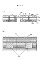
- Figures 12 (a) and 12 (b) are diagrams which show a bending rigid printed wiring board in which a circuit for large current and a circuit for small current are formed on the same surface, Figure 12(a) being a sectional view and Figure 12(b) being a plan view.
- a circuit for large current 14 a having a thickness of not less than 200 ⁇ m and circuits for small current 14b 1 , 14b 6 having a thickness of 18 to 70 ⁇ m are formed on the same surface, with the height of these circuits being flush with each other.
- the circuit for large current 14 a and the circuits for small current 14b 1 , 14b 6 are formed on the front surface (the outermost layer) of the bending rigid printed wiring board, and the electrically conducting properties of these circuits are ensured via through holes 7 and circuits formed on the inner side (circuits for small current 14b 3 , 14b 4 ).
- the electrically conducting properties of the circuits for small current (14b 1 , 14b 2 , 14b 5 , 14b 6 ) formed by etching the thin conductors 43a, 43b of the conductor laminate material 44 buried in the hole portion 41 of the conductor plate 40 and the circuit for large current 14a formed by etching the conductor plate 40 are ensured, as shown in Figure 12(a) , by the medium of a through hole 7 (a via through hole) provided in the section where the circuits for small current (14b 1 , 14b 2 , 14b 5 , 14b 6 ) are formed, a through hole 7 (via through hole) provided in the section where the circuit for large current 14a is formed, and the circuits for small current (14b 3 , 14b 4 ) provided on the front surface or rear surface of the core material 1'.
- the front surface and rear surface of the bending rigid printed wiring board are coated with a resist (an insulating material) 9 in order to protect the circuits.
- a bending rigid printed wiring board 10 having a bent portion 10A which is formed by partially reducing the thickness of a hard base material 5 was used, and after the installation of connection terminals 20 to the front surface of this bending rigid printed wiring board 10, the bending rigid printed wiring board 10 was bent at a bent portion 10A, whereby a substrate circuit in which the connection terminals 20 are provided at prescribed positions on both surfaces was manufactured.
- circuits 14 are formed on the front surface and rear surface of the hard base material 5 and at the same time, via through holes 7a for ensuring the electrically conducting properties of the circuits formed on the above-described front surface and rear surface are formed.
- a bent portion 10A which is obtained by partially reducing the thickness of the hard base material 5 is formed and at the same time, in the substrate (the base material 5) arranged right and left with the bent portion 10A interposed, there are formed mounting through holes 7b for arranging the connection terminals 20 at prescribed positions.
- the circuit 14 is formed on the front surface of the bent portion 10A which is obtained by partially reducing the thickness of the hard base material 5 and this ensures the connection of the circuits formed on the front surface of the substrate (the base material 5) arranged right and left with the bent portion 10A interposed.
- the circuit surfaces are coated with the resist (the insulating material) 9.
- the resist the insulating material
- connection terminals 20 are press fitted into the mounting through holes 7b and the connection terminals 20 are provided at prescribed positions on the front surface of the rigid printed wiring board 10 (refer to Figure 13 (b) ), on the rear surface of the rigid printed wiring board 10 leading end portions 20A of the press-fitted connection terminals 20 are soldered 21, whereby the connection terminals 20 are fixed to the rigid printed wiring board 10 (refer to Figure 13(c) ).
- the bent portion 10A of the rigid printed wiring board 10 in which the connection terminals 20 are provided at prescribed positions on the front surface by use of a bending jig 30 it is possible to easily manufacture a substrate circuit in which the connection terminals 20 are provided at prescribed positions on both surfaces as shown in Figure 13(a) .
- connection terminals 20 are press fitted into the above-described mounting through holes 7b and soldered, whereby the connection terminals 20 are provided at prescribed positions on the front surface.
- the heat resistant resin material 2 buried in the above-described gap portion 1A is removed and a bent portion 10A which is obtained by partially reducing the thickness of the hard base material 5 is formed and the rigid printed wiring board 10 is bent thereafter in the above-described bent portion 10A, whereby a substrate circuit in which the connection terminals 20 are provided at prescribed positions on both surfaces is manufactured.
- the substrate circuit shown in Figure 14 (a) is fabricated by bending a rigid printed wiring board 10, in which the connection terminals 20 are provided at prescribed positions on the front surface, in the bent portion 10A. Therefore, the degree of freedom of the positions of the connection terminals 20 which are provided at prescribed positions on the front surface and the rear surface is high and besides it is necessary only that the soldering step for fixing the connection terminals 20 to the substrate be performed once. Furthermore, for the circuits which are formed in the substrate (base material 5) which is arranged, with the bent portion 10A interposed, electrical connection is ensured by the circuit 14 formed on the front surface of the bent portion 10A.
- an insulating film 91 is provided on the front surface of the bent portion 10A.
- the rigid printed wiring board in which the bent portion 10A is not coated with the resist 9 was bent, and after that, the insulating film 91 was provided on the front surface of the bent portion 10A in order to protect the circuit 14 formed on the front surface of the above-described bent portion 10A.
Landscapes
- Engineering & Computer Science (AREA)
- Microelectronics & Electronic Packaging (AREA)
- Manufacturing & Machinery (AREA)
- Production Of Multi-Layered Print Wiring Board (AREA)
- Structure Of Printed Boards (AREA)
Abstract
Description
- The present invention relates to a printed wiring board which permits easy mounting of electrical parts and the like and which not only enables spaces to be saved, but also facilitates manufacturing.
- Electrical components tend to increase in number from the requirements for an improvement in the functions of products of, for example, automobiles. For this reason, in order to use limited spaces efficiently, it is required that electrical parts and the like be easily mounted and that spaces necessary for their mounting be reduced.
Therefore, in performing the wiring and branching of electric wires for automobiles and the like, there has been used an electric connection box which is constructed so that parts, such as connections to wire harness, fuses and relays, are collected in one place and connected there. And as the above-described electric connection box, there has been known an electric connection box in which a rigid printed wiring board that is constructed in such a manner that a circuit is formed on the surface of a hard base material is used as a wiring material for distributing power from a power source (hereinafter referred to as an internal circuit). - A method of manufacturing a rigid printed
wiring board 100 by prior art will be described with reference toFigures 15 (a) to 15(c) .
According to the prior art, alaminate 103 which is obtained by laminating aconductor layer 102, such as copper foil and silver foil, each on a front surface and a rear surface of ahard base material 101 made of an insulating material, is used (refer toFigure 15(a) ), and through holes 104 (a via throughhole 104a which ensures electrically conducting properties for theconductor layers 102 on the front and rear surfaces and a mounting throughhole 104b for providing a connection terminal 20) are formed by planting a substrate through-hole provided by drilling thelaminate 103. At the same time, by etching the above-describedlaminate 103, acircuit 102a is formed on the front and rear surfaces of the hard base material 101 (refer toFigure 15 (b) ), and the front surface of the circuit is coated with a resist (an insulating material) 105, whereby a rigid printedwiring board 100 is manufactured (refer toFigure 15(c) ). Also, a multilayer wiring board has been similarly manufactured by performing laminating and pressing. - In a case where by use of the prior art, an electrical part is mounted on the rigid printed
wiring board 100 and a wiring material (a substrate circuit) of an internal circuit as used in electrical equipment is formed, as shown inFigures 16 (a) to 16 (c) , the mounting throughhole 104b for the insertion of theconnection terminal 20 is provided beforehand in a connector for the connection to the electrical part and a connection to the electrical part, such as a fuse and a relay. After the press fitting of theconnection terminal 20 into the above-described mounting throughhole 104b, the rigid printedwiring board 100 and theconnection terminal 20 are connected together after going through the step of flow soldering or reflow soldering.
As shown inFigure 16(a) , in connecting theconnection terminal 20 to the rigid printedwiring board 100 which is provided with the via throughhole 104a for ensuring the conducting properties of the circuits formed on the front and rear surfaces of the substrate and the mounting throughhole 104b into which theconnection terminal 20 is press fitted, because the above-described mounting throughhole 104b is formed from a hole which pierces through the substrate, in a case where a substrate circuit in which theconnection terminals 20 are provided at prescribed positions each on the front surface and rear surface of the substrate, it is necessary to design a substrate circuit in such a manner that the positions of theconnection terminals 20 do not overlap on the front and rear surfaces. Therefore, the prior part had the disadvantage that the projected area of the substrate circuit becomes large.
In forming a substrate circuit in which theconnection terminals 20 are provided at prescribed positions each on the front surface and rear surface of the substrate, it was necessary to solder theconnection terminals 20 by performing the step of fixing theconnection terminals 20 provided at prescribed positions on the front surface of the rigid printedwiring board 100 bysolders 21 as shown inFigure 16 (b) , and the step of fixing theconnection terminals 20 provided at prescribed positions on the rear surface of the rigid printedwiring board 100 bysolders 21 as shown inFigure 16(c) . That is, it has been necessary to perform the soldering step twice. - Therefore, as shown in
Figures 17(a) and 17(b) , there have been proposed techniques which involve connecting two rigid printedwiring boards 100, in each of which aconnection terminal 20 is provided at a prescribed position on a front surface, by means of anelectric wire 107, and bending the two rigid printedwiring boards 100 in an electric wire portion, whereby a substrate circuit in which theconnection terminals 20 are provided at prescribed positions on both surfaces is obtained (refer toPatent Document 1, for example).
[Patent Document 1]Japanese Patent Application No. 2004-192546 - In a substrate circuit which is formed in such a manner that two rigid printed
wiring boards 100 connected together by anelectric wire 107 are bent in the above-described electric wire portion,connection terminals 20 which are provided at prescribed positions on each of the front surfaces of the two rigid printedwiring boards 100 connected together by theelectric wire 107 are soldered and fixed (refer toFigure 17 (a) ), and after that, the two rigid printedwiring boards 100 are bent in the above-described electric wire portion, whereby a substrate circuit in which the connection terminals are provided at prescribed positions on both surfaces is obtained (refer toFigure 17 (b) ). Therefore, it is necessary only that the soldering step for fixing theconnection terminals 20 be performed once and besides theconnection terminals 20 can be provided at arbitrary positions on both surfaces of the substrate.
However, it is necessary to install theelectric wire 107 in such a manner that the circuits of the two rigid printedwiring boards 100 are connected together, and it takes time to perform this wire installation step. At the same time, the larger the number of theelectric wires 107 for connecting the circuits of the substrates, the more difficult to bend the two rigid printed wiring boards in the electric wire portion will be. Besides the prior art has had the disadvantage that the space occupied by theelectric wire 107 after the bending becomes large. Furthermore, because it is difficult to completely make equal the length of each of the electric wires 017 which connect the circuits of the two rigid printedwiring boards 100, it has been difficult to uniformly control the shape after the bending. - In the present invention, therefore, in a rigid printed wiring board which is formed in such a manner that an arbitrary circuit is formed on a front surface of a hard base material by etching a laminate, a bent portion obtained by partially reducing the thickness of the base material is provided so that the rigid printed wiring board can be bent in this bent portion.
Also, a circuit for large current (for example, an inner circuit of an electric connection box) and a circuit for small current (for example, an electronic circuit) are formed in a bending rigid printed wiring board, whereby the substrate performance can be improved. - In a bending rigid printed wiring board of the present invention, a heat resistant resin layer is laminated on a front surface of a hard core material provided so as to contain a gap portion and also on a top surface of the gap portion, a heat resistant resin layer is laminated on a rear surface of the core material except the gap portion, a conductor layer is laminated and firmly fixed via the heat resistant resin layers, and the conductor layer is etched, whereby a circuit is formed.
Conductor portions having different layer thicknesses are formed on the same surface of the conductor, whereby a circuit for large current and a circuit for small current are formed on the same substrate. - A method of manufacturing a bending rigid printed wiring board of the present invention comprises a step of burying a heat resistant resin material in a gap portion provided in a hard core material, a step of forming a laminate by laminating a conductor layer each on a front surface and a rear surface of the hard core material via heat resistant resin layers and performing hot pressing, a step of forming a circuit on the front surface and rear surface of the hard base material by etching the laminate and of removing the conductor layer on the rear surface of the gap portion of the hard core material, and a step of removing the heat resistant resin material buried in the gap portion along with the heat resistant resin material on the rear surface of the heat resistant resin material, whereby a bent portion obtained by partially reducing the thickness of the hard base material is formed. A rigid printed wiring board capable of being bent in the bent portion is obtained by performing the steps.
- According to a bending rigid printed wiring board of the present invention, by providing a bent portion obtained by partially reducing the thickness of the hard base material, it is possible to bend the printed wiring board in the bent portion.
In a case where an electrical part is mounted on the bending rigid printed wiring board of the present invention and a wiring material (a substrate circuit) of an internal circuit as used in electrical equipment is formed, after the provision of connection terminals at prescribed positions on a front surface of the rigid printed wiring board, the rigid printed wiring board is bent in the above-described bent portion, whereby it is possible to obtain a substrate circuit in which the connection terminals are provided on both surfaces. Therefore, the installation positions of the connection terminals can be arbitrarily designed and the soldering step of the connection terminals is performed only once. Furthermore, unlike a substrate circuit in which two rigid printed wiring boards connected together by an electric wire are bent in the electric wire portion, one rigid printed wiring board is bent in a bent portion obtained by partially reducing the thickness of a hard base material and, therefore, it is unnecessary to install electric wires for connecting together the circuits of opposed substrate surfaces. - Furthermore, in the bending rigid printed wiring board of the present invention, a gap portion is formed beforehand in part of the hard core material and a heat resistant resin material is buried in this gap portion. And at the same time, a laminate which is obtained by laminating a conductor layer on the front surface and rear surface of the hard core material via a heat resistant resin layer is used, and a heat resistant resin material buried in the gap portion is removed from the above-described laminate, whereby it is possible to easily form a bent portion which is obtained by partially reducing the thickness of the hard base material. Unlike a rigid-flexible substrate of multilayer structure which is constituted by multiple layers of a polyimide film and the like, which have different properties, and combines a flexible portion and a rigid portion, the bending rigid printed wiring board is simple in construction and can be manufactured at low cost.
Moreover, in manufacturing the bending rigid printed wiring board, conductor portions having different layer thicknesses are formed on the same surface of the conductor layer and a circuit for large current (for example, an inner circuit of an electric connection box) and a circuit for small current (for example, an electronic circuit) are formed, whereby it is possible to improve the substrate performance. -
-
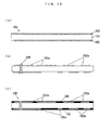
Figures 1 (a) to 1(d) are sectional views which explain a method of manufacturing a laminate; -
Figures 2(a) to 2(c) are plan views which show a heat resistant resin material buried in a gap portion; -
Figures 3(a) to 3(d) are sectional views which explain a method of manufacturing a bending rigid printed wiring board according to the present invention; -
Figures 4 (a) to 4(d) are sectional views which explain a method of manufacturing a bending rigid printed wiring board in another embodiment; -
Figures 5 (a) to 5(c) are sectional views which explain a method of manufacturing a bending rigid printed wiring board (a single-side wiring board); -
Figures 6(a) to 6(e) are sectional views which explain a method of manufacturing a bending rigid printed wiring board (a multilayer wiring board); -
Figures 7(a) to 7(d) are partial sectional views which explain a method of manufacturing a bending rigid printed wiring board provided with conductor portions having different layer thicknesses on the same surface; -
Figures 8 (a) to 8(c) are first explanatory diagrams of a method of manufacturing a bending rigid printed wiring board in which a circuit for large current and a circuit for small current are formed on the same surface; -
Figures 9(a) and 9(b) are second explanatory diagrams of a method of manufacturing a bending rigid printed wiring board in which a circuit for large current and a circuit for small current are formed on the same surface; -
Figures 10 (a) and 10 (b) are third explanatory diagrams of a method of manufacturing a bending rigid printed wiring board in which a circuit for large current and a circuit for small current are formed on the same surface; -
Figures 11 (a) to 11 (d) are fourth explanatory diagrams of a method of manufacturing a bending rigid printed wiring board in which a circuit for large current and a circuit for small current are formed on the same surface; -
Figures 12 (a) and 12 (b) are fifth explanatory diagrams of a method of manufacturing a bending rigid printed wiring board in which a circuit for large current and a circuit for small current are formed on the same surface; -
Figures 13 (a) to 13 (d) are sectional views which explain a method of manufacturing a substrate circuit in which connection terminals are provided at prescribed positions in a bending rigid printed wiring board; -
Figures 14 (a) and 14 (b) are sectional views of a substrate circuit in which connection terminals are provided at prescribed positions; -
Figures 15 (a) to 15 (c) are sectional views which explain a method of manufacturing a rigid printed wiring board by prior art; -
Figures 16 (a) to 16 (c) are sectional views of a substrate circuit in which connection terminals are provided at prescribed positions in a rigid printed wiring board by prior art; and -
Figures 17(a) and 17(b) are diagrams which show other examples of the method shown inFigures 15(a) to 15(c) . -
- 1
- Hard core material
- 11
- Core material as a shielded plate
- 1A
- Gap portion
- 2
- Heat resistant resin material
- 31, 32
- Heat resistant resin layer
- 32A
- Notch
- 4
- Conductor layer, copper layer
- 4A
- Thick conductor portion
- 4B
- Thin conductor portion
- 14
- Circuit
- 14a
- Circuit for large current
- 14b1 to 14b6
- Circuit for small current
- 5, 51 to 54
- Hard base material
- 6, 61 to 64
- Laminate
- 7
- Through hole
- 7a
- Via through hole
- 7b
- Mounting through hole
- 8
- Exposed portion
- 9
- Resist
- 91
- Insulating film
- 10
- Rigid printed wiring board
- 10A
- Bent portion
- 20
- Connection terminal
- 21
- Solder
- 30
- Bending jig
- 40
- Conductor plate
- 41
- Hole portion
- 42
- Insulating base material
- 43
- Conductor
- 44
- Conductor laminate material
- A bending rigid printed wiring board and a method of manufacturing the bending rigid printed wiring board in embodiments of the present invention will be described with reference to
Figure 1 to Figures 15(a) to 15(c) . - The bending rigid printed
wiring board 10 of this embodiment is such that in a bending rigid printedwiring board 10 in which anarbitrary circuit 14 is formed by etching alaminate 6 which is obtained by laminating aconductor layer 4 each on the front surface and rear surface of ahard base material 5, abent portion 10A which is obtained by partially reducing the thickness of the above-describedhard base material 5 is formed.
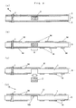
In this embodiment, as shown inFigures 1(a) to 1(d) (sectional views) which illustrate the manufacturing process of a laminate, ahard core material 1 from which a portion corresponding to the bent portion has been removed is used and a heatresistant resin material 2 is buried in a relevant gap portion (the portion from which the hard core material has been removed) 1A. And aconductor layer 4 is laminated each on the front surface and rear surface of thehard core material 1, in which the heatresistant resin material 2 is buried in thegap portion 1A, via heat resistant resin layers 31, 32, and after that, hot pressing is performed, whereby thelaminate 6 in which theconductor layer 4 is laminated each on both surfaces of thehard base material 5 is fabricated. - In the embodiment shown in
Figures 1(a) to 1(d) , ahard core material 1 formed from a glass epoxy resin is used. In the center part of the flat-pate-likehard core material 1 having a layer thickness of 0.4 mm, there is provided agap portion 1A which is obtained by removing part of the core material in groove form, whereby thegap portion 1A was formed in a place corresponding to the bent portion (refer toFigure 1(a) ).
And a heatresistant resin material 2, such as a Teflon (registered trademark) sheet having a film thickness of 0.4 mm and silicone rubber, is buried in the above-describedgap portion 1A, whereby thehard core material 1 in which the heatresistant resin material 2 is buried at a position corresponding to the bent portion is fabricated (refer toFigure 1 (b) ).
By forming thegap portion 1A beforehand in part of the hard core material, it is possible to easily reduce part of the thickness of the hard base material by removing, in a succeeding step, the heatresistant resin material 2 buried in thisgap portion 1A.
Also, by burying the heatresistant resin material 2 in thegap portion 1A of thehard core material 1, it is possible tomake the pressure during hot pressing uniform in a succeeding step (during the fabrication of thelaminate 6 by laminating the conductor layer 4). - After the burying of the heat
resistant resin material 2 in thegap portion 1A, acopper layer 4 having a film thickness of 200 µm to 600 µm is laminated (refer toFigure 1 (c) ) each on the front surface and rear surface of the above-describedhard core material 1 via heat resistant resin layers 31, 32 having a film thickness of 0.1 mm (corresponding to adhesive layers for bonding the copper layer 4) and hot pressing is performed, whereby thelaminate 6 in which thecopper layer 4 is bonded to both surfaces of thehard base material 5 is fabricated(refer toFigure 1(d) ).
In this embodiment, abonding sheet 31 having a layer thickness of 0.1 mm and a glass epoxy resin sheet (a prepreg) 32 having a layer thickness of 0.1 mm were used as the heat resistant resin layers 31, 32.
And thecopper layer 4 was laminated on the front surface of thehard core material 1 in which the heatresistant resin material 2 is buried in thegap portion 1A via thebonding sheet 31 and, at the same time, thecopper layer 4 was laminated on the rear surface of thehard core material 1 via the glass epoxy resin sheet (the prepreg) 32 and hot pressed, whereby thelaminate 6 in which thecopper layer 4 is bonded to both surfaces of thehard base material 5 was fabricated.
Incidentally, it is also possible to fabricate a laminate obtained by laminating thecopper layer 4 on both surfaces of thehard core material 1 via a bonding sheet or a laminate obtained by laminating thecopper layer 4 on both surfaces of thehard core material 1 via a glass epoxy resin sheet (a prepreg). - When hot pressing is performed, the heat resistant resin layers 31, 32 (bonding sheets or glass epoxy resin sheets (prepregs)) cure thermally and the heat resistant resin layers 31, 32 become bonded to (become integral with) the
hard core material 1, whereby thehard base material 5 having a layer thickness of 0. 6 mm is formed and, at the same time, thecopper layer 4 becomes bonded via the heat resistant resin layers 31, 32, with the result that it is possible to obtain thelaminate 6 in which thecopper layer 4 is bonded to both surfaces of thehard base material 5.
Incidentally, when a glass epoxy resin sheet (a prepreg) is laminated on thehard core material 1 formed from a glass epoxy resin and hot pressing is performed, thehard core material 1 and the glass epoxy resin sheet (the prepreg) become integral with each other. - Furthermore, in this embodiment, as shown in the plan views of
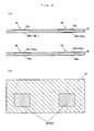
Figures 2 (a) to 2 (c) , by burying the heatresistant resin material 2 beforehand in thegap portion 1A formed in thehard core material 1, it is possible to keep the shape of thegap portion 1A during hot pressing. Also, the pressure during hot pressing become equal and thelaminate 6 can be fabricated without the formation of a recess in thegap portion 1A.
As shown inFigure 2(a) , thegap portion 1A which is obtained by removing part of thecore material 1 in groove form was provided in the middle part of thehard core material 1, the heatresistant resin material 2 was buried in thisgap portion 1A, and the heat resistant resin layers 31, 32 were laminated on the front surface and rear surface of the hard core material.
Incidentally, in the embodiment shown inFigure 2(a) , the groove-shapedgap portion 1A was formed by removing part of thecore material 1, the heatresistant resin material 2 was buried in thisgap portion 1A, and the heat resistant resin layers 31, 32 were laminated on the front surface and rear surface of the core material. However, it is also possible to use multiplehard core materials 1 and to arrange the core materials at specified intervals so as to formcore materials 1 having agap portion 1A.
It is also possible to laminate a heat resistant resin layer 32' , in which anotch 32A similar to the above-describedgap portion 1A is made, on the rear surface of thecore material 1 in which the heatresistant resin material 2 is buried in thegap portion 1A and to laminate thecopper layer 4 via the heat resistant resin 32' (refer toFigures 4(a) to 4(d) ). - By laminating the
copper layer 4 on both surfaces of thehard core material 1, in which the heatresistant resin material 2 is buried in thegap portion 1A, via the above-described heat resistant resin layers 31, 32, and performing hot pressing, it is possible to fabricate thelaminate 6 which is obtained by bonding thecopper layer 4 to thehard base material 5, with the shape of thegap portion 1A formed in thehard core material 1 kept and without the formation of a recess in the above-describedgap portion 1A.
And in this embodiment, after the formation of thecircuit 14 and a through hole 7 (a via throughhole 7a and a mounting throughhole 7b) in the above-describedlaminate 6, the edge portions of thelaminate 6 were cut (refer toFigure 2(b) ) and the heatresistant resin material 2 buried in thegap portion 1A was removed, whereby the bending rigid printedwiring board 10 in which thebent portion 10A is arranged so as to traverse the middle of the substrate was obtained (refer toFigure 2 (c) ). Incidentally, before the cutting of the edge portions, the heatresistant resin material 2 may be removed from thegap portion 1A. - According to this embodiment, as shown in
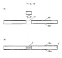
Figures 3 (a) to 3(d), which illustrate the manufacturing process of a rigid printed wiring board,arbitrary circuits 14 are formed on the front surface and rear surface of thehard base material 5 by etching thelaminate 6 and the through hole 7 (the via throughhole 7a which ensures the conducting properties of the circuits formed on the front surface and rear surface of the substrate and the mounting throughhole 7b for providing the connection terminals at prescribed positions) is formed.
And after that, the heatresistant resin material 2 buried in thegap portion 1A of thehard core material 1 is removed along with the heatresistant resin layer 32 laminated on the rear surface of the heatresistant resinmaterial 2, whereby thebent portion 10A obtained by reducing the thickness of thehard base material 5 in part is formed. - In the embodiment shown in
Figures 3(a) to 3(d) , a hole was made at a necessary position of thelaminate 6 obtained by bonding thecopper layer 4 on both surfaces of thehard base material 5 and this holed place (a through hole of the substrate) was plated, whereby the through hole 7 (the via throughhole 7a which ensures the conducting properties of the copper layers 4 formed on both surfaces of the hard base material and the mounting throughhole 7b for providing the connection terminals at prescribed positions) was formed (refer toFigure 3(a) ) and the above-describedlaminate 6 was etched, whereby thearbitrary circuits 14 were formed on both surfaces of the above-described hard base material 5 (refer toFigure 3(b) ).
Incidentally, in etching thelaminate 6 and forming thearbitrary circuits 14 on the rear surface of thehard base material 5, thecopper layer 4 at a position corresponding to thegap portion 1A of the hard core material 1 (on the rear surface of the heat resistant resin material 2) is removed by etching beforehand (an exposed portion 8). - And the heat
resistant resin layer 32 was cut in the above-describedexposed portion 8 and removed along with the heatresistant resin material 2 buried in thegap portion 1A, whereby thebent portion 10A obtained by partially reducing the thickness of thehard base material 5 was formed (refer toFigure 3(d) ).
That is, by removing the heatresistant resin material 2 buried in thegap portion 1A along with the heatresistant resin layer 32 on the rear surface, a thin-walled portion consisting of the heat resistant resin layer 31 (bonding sheet) having a film thickness of 0.1 mm, which is a single layer, is formed in part of thehard base material 5 and the rigid printed wiring board can be bent in this thin-walled portion (thebent portion 10A). - In the bending rigid printed
wiring board 10 in this embodiment, on the front surface of the thin-walled portion consisting of the heat resistant resin layer 3 (the bonding sheet 31), which is a single layer, there is formed thecircuit 14 made by etching thecopper layer 4 having a layer thickness of 200 µm to 600 µm and it is ensured that circuits formed on the front surface of thehard base material 5 are connected together, the hard base material being arranged right and left, with thebent portion 10A interposed. - Next, with reference to
Figures 4(a) to 4(d) , a description will be given of a method of manufacturing a bending rigid printedwiring board 10 which involves laminating aconductor layer 4 on the front surface of ahard core material 1 in which a heatresistant resin material 2 is buried in agap portion 1A via a heatresistant resin layer 31, at the same time laminating aconductor layer 4 on the rear surface of thehard core material 1 via a heat resistant resin layer 32' in which anotch 32A similar to the above-describedgap portion 1A is made, performing hot pressing, whereby a laminate 61 in which the conductor layers 4 are bonded to both surfaces of thehard base material 51 is fabricated, and removing the heatresistant resin material 2 buried in thegap portion 1A from thislaminate 61. - In the embodiment shown in
Figures 4 (a) to 4 (d) , in the same way as with the embodiment shown inFigures 1(a) to 1(d) , in the center part of the flat-plate-likehard core material 1 which is made of a glass epoxy resin and has a layer thickness of 0. 4 mm, there is provided thegap portion 1A which is formed by removing part of the core material in groove form.
And in this embodiment, a heatresistant resin material 2, such as a Teflon (registered trademark) sheet having a film thickness of 0.5 mm and silicone rubber, was buried in thegap portion 1A of thehard core material 1, and a convex portion having a height of 0.1 mm was formed, the convex portion being such that the heatresistant resin material 2 protrudes from the rear surface of thegap portion 1A. Also, thenotch 32A corresponding to the above-described convex portion was formed in the heat resistant resin layer 32' laminated on the rear surface of thehard core material 1, and thecopper layer 4 having a layer thickness of 200 to 600 µm was laminated each on the front surface and rear surface of thehard core material 1, in which the heatresistant resin material 2 is buried in thegap portion 1A, via the heat resistant resin layers 31, 32' (refer toFigure 4(a) ). - When the
copper layer 4 is laminated, via the heatresistant resin layer 31, on the front surface of thehard core material 1, in which the heatresistant resin material 2 is buried in thegap portion 1A, thecopper layer 4 is laminated on the rear surface via the heat resistant resin layer 32' in which thenotch 32A is made, and hot pressing is performed, the above-described heat resistant resin layers 31, 32' cure thermally and become bonded to (become integral with) thehard core material 1 and thehard base material 51 having a layer thickness of 0.6 mm is formed and, at the same time, thecopper layer 4 becomes bonded via the above-described heat resistant resin layers 31, 32' , whereby it is possible to obtain the laminate 61 in which thecopper layer 4 is laminated on both surfaces of thehard base material 51. - Incidentally, in this example, the
copper layer 4 is laminated on the rear surface of the heatresistant resin material 2 buried in thegap portion 1A without the interposition of the heat resistant resin layer 32'. - After that,
arbitrary circuits 14 are formed on the front surface and rear surface of thehard base material 51 by etching the laminate 61 and at the same time, a through hole 7 (a via throughhole 7a which ensures the conducting properties of the circuits formed on the front surface and rear surface of the substrate and a mounting throughhole 7b for providing connection terminals at prescribed positions) is formed. - Incidentally, in etching the laminate 61 and forming the
arbitrary circuits 14 on the rear surface of thehard base material 5, thecopper layer 4 on the rear surface of the heatresistant resin material 2 buried in thegap portion 1A is removed by etching beforehand (an exposed portion 8) . - And in this embodiment, as shown in
Figure 4(d) , by removing the heatresistant resin material 2 buried in thegap portion 1A of thehard core material 1, abent portion 10A which is obtained by reducing the thickness of part of thehard base material 51 is formed. - In a both-side wiring board in which the
circuits 14 are formed on the front surface and rear surface of thehard base material 51, a bending rigid printedwiring board 10 provided with abent portion 10A which is obtained by partially reducing the thickness of thehard base material 51 has been described above. However, the bending rigid printed wiring board is not limited to the both-side wiring board. - For example, as shown in
Figures 5(a) to 5(c) , a laminate 62 which is obtained by laminating, via a heat resistant resin layer 3, aconductor layer 4 on the front surface (a single side) of ahard core material 1, in which a heatresistant resin material 2 is buried in agap portion 1A, is used (refer toFigure 5(a) ), and, by etching the laminate,circuits 14 are formed on the front surface of thehard base material 52 constituted by thehard core material 1 and the heat resistant resin layer 3 (refer toFigure 5(b) ). At the same time, the heatresistant resin material 2 buried in thegap portion 1A of thehard core material 1 is removed and a thin-walled portion constituted by only a heat resistant resin layer 3, which is a single layer, is provided in part of thehard base material 52, whereby it is possible to obtain a bending rigid printed wiring board (a single-side wiring board) having abent portion 10A formed by partially reducing the thickness of the hard base material 52 (refer toFigure 5(c) ). - Also, for example, as shown in
Figures 6(a) to 6(e) , by using acore material 11 in the form of a shielded plate, it is possible to obtain a bending rigid printed wiring board (a multilayer wiring board) having abent portion 10A obtained by partially reducing the thickness.
As shown inFigures 6(a) to 6(d) , ahard core material 1 is laminated, via a heatresistant resin layer 31, on the front surface of a rigid wiring board in whichcircuits 14 are formed on the front surface of ahard core material 1 and hot pressing is performed, whereby ahard core material 11 in the form of a shielded plate is fabricated (refer toFigure 6(a) ), agap portion 1A is formed by removing part of thehard core material 11 in the form of a shielded plate (refer toFigure 6(b) ), aconductor layer 4 is laminated, via a heatresistant resin layer 31, on the front surface of thecore material 11 in the form of a shielded plate in which a heatresistant resin material 2 is buried in the above-describedgap portion 1A, aconductor layer 4 is laminated on the rear surface via a heat resistant resin layer 32' in which anotch 32A is made, and hot pressing is performed, whereby a laminate 63 in which the conductor layers 4 are laminated on both surfaces of ahard base material 53 is fabricated (refer toFigure 6(c) ). And thecircuits 14 are formed on the front surface and rear surface of thehard base material 53 by etching the above-describedlaminate 63 and at the same time, theconductor layer 4 on the rear surface of the gap portion 1a is removed by etching (refer toFigure 6(d) ) and furthermore, the heatresistant resin material 2 buried in the above-describedgap portion 1A is removed, whereby it is possible to obtain a multilayer wiring board having abent portion 10A which is formed by partially reducing the thickness (refer toFigure 6(e) ). - Next, with reference to
Figures 7 (a) to 7 (d) toFigures 12(a) and 12(b) , a description will be given of a method of manufacturing a bending rigid printed wiring board in which a circuit for large current and a circuit for small current are formed on the same substrate by forming conductor parts (4A, 4B) having different layer thicknesses on the same surface of aconductor layer 4. -
Figures 7(a) to 7(d) are diagrams to explain a method of formingconductor layer 4 which is constituted by athick conductor portion 4A having a thickness of not less than 175 µm, preferably 200 to 600 µm, and athin conductor portion 4B having a thickness of not more than 105 µm, preferably 18 to 70 µm. In this embodiment, aconductor plate 40 having a thickness of not less than 175 µm, preferably 200 to 600 µm and aconductor laminate material 44 which is formed to suit the shape of the above-described hole portion and the thickness of the conductor plate (aconductor laminate material 44 formed by laminating a thin conductor 43) are used. - First, as shown in
Figure 7(a) , theconductor plate 40 having a thickness of not less than 175 µm, preferably 200 to 600 µm is prepared, and ahole portion 41 is formed in thisconductor plate 40.
As shown inFigure 7(b) , theconductor laminate material 44, which is obtained by laminating a thin conductor 43 (aconductor 43 having a thickness of not more than 100 µm, preferably 18 to 70 µm) on an insulatingbase material 42, is formed to suit the thickness of the above-describedconductor plate 40 and the shape of thehole portion 41.
And as shown inFigure 7(c) , theconductor laminate material 44 obtained by laminating thethin conductor 43 is buried (embedded) in thehole portion 41 of theconductor plate 40. And theconductor plate 40, in which theconductor laminate material 44 is buried in thehole portion 41, is laminated on acore material 1 via a heat resistant resin layer (31 or 32) and hot pressing is performed, whereby as shown inFigure 7 (d) , the conductor portions havingdifferent layer thicknesses conductor layer 4. That is, upon the same surface of theconductor layer 4, there are formed thethick conductor portion 4A having a thickness of not less than 175 µm, preferably 200 to 600 µm, and thethin conductor portion 4B having a thickness of not more than 105 µm, preferably 18 to 70 µm. Incidentally, in abent portion 10A of a bending rigid printed wiring board, theconductor plate 40 is laminated so that thethick conductor portion 4A having a thickness of not less than 175 µm can be provided. - Subsequently, with reference to
Figures 8(a) to 8(c) toFigures 12(a) and 12(b) , a description will be given of a method of manufacturing a bending rigid printed wiring board in which a circuit for large current and a circuit for small current are formed on the same surface.
In this embodiment, by using the technique shown inFigures 7(a) to 7(d) , a bending rigid printedwiring board 10 is manufactured, in which a circuit for large current 14a having a thickness of not less than 175 µm, preferably 200 to 600 µm (for example, an inner circuit of an electric connection box) and a circuit for small current 14b having a thickness of not more than 105 µm, preferably 18 to 70 µm (for example, an electronic circuit) are formed. - In this embodiment, as shown in
Figure 8(a) , there are prepared aconductor plate 40 having a thickness of not less than 200 µm and a conductor laminate parent material 44' having the same thickness as this conductor plate. Incidentally, a conductor laminate parent material obtained by laminatingthin conductors base material 42 was used as the conductor laminate parent material 44' .
And as shown inFigure 8 (b) , ahole portion 41 is formed by partially boring theconductor plate 40 and at the same time, as shown inFigure 8(c) , aconductor laminate 44 is cut out of the conductor laminate parent material 44' to suit the shape of ahole portion 41 of the above-describedconductor plate 40.
In this embodiment, twohole portions 41 were made each in twoconductor plates 40 and fourconductor laminate materials 44 were cut out of one conductor laminate parent material 44' to suit the shape of thehole portion 41. - And as shown in the sectional view of
Figure 9 (a) , the conductor laminates 44, in which thethin conductors respective hole portions 41, and as shown in the plan view ofFigure 9 (b) , thethin conductors conductor plate 40 having a thickness of not less than 200 µm. Incidentally because theconductor plate 40 and theconductor laminate material 44 have the same thickness, the front surface of the conductor and thethin conductors
In this embodiment, thethin conductor 43b on one side of the above-describedconductor laminate material 44 was etched, circuits for small current (14b2, 14b5) were formed beforehand, and theconductor laminate materials 44 were buried in thehole portions 41 of theconductor plates 40 so that these circuits for small current (14b2, 14b5) are arranged on the inner side. That is, it was ensured that the circuits for small current (14b2, 14b5) are formed on athin conductor 43b which are arranged on the inner side when theconductor plates 40, in which theconductor laminate material 44 is buried, are each laminated on the front surface and rear surface of the hard core material via heat resistant resin layers 31, 32, are formed beforehand. - In the manufacturing process of a bending rigid printed wiring board, in this embodiment, a hard core material obtained by laminating
thin conductors Figure 10 (a) ). And a heatresistant resin material 2 is buried in a gap portion (a portion from which the hard core material has been removed) 1A of the hard core material 1' on which thethin conductors thin conductors - And as shown in
Figures 11(a) to 11(d) , theconductor plates 40, in which theconductor laminate material 44 is buried in thehole portion 41, are laminated, via the heat resistant resin layers 31, 32, on the front surface and rear surface of the hard core material 1' in which the heatresistant resin material 2 is buried in thegap portion 1A and hot pressing is performed, whereby a laminate 64 is fabricated (refer toFigures 11(a) and 11(b) ).
As shown inFigure 11(b) , athick conductor portion 4A having a thickness of not less than 200 µm and athin conductor portion 4B (athin conductor 43a) having a thickness of 18 to 70 µm are formed on the conductor layers 4 on the front surface and rear surface of the laminate 64 fabricated by laminating theconductor plate 40, in which theconductor laminate material 44 is buried in thehole portion 41.
And as shown inFigure 11(c) , circuits for small current 14b1, 14b6 having a thickness of 18 to 70 µm were formed by etching the above-describedthin conductor portion 4B (thethin conductor 43a) and at the same time, a circuit for large current 14a having a thickness of not less than 200 µm was formed by etching the above-describedthick conductor portion 4A. Thus, the circuit for large current 14a and the circuits for small current 14b1, 14b6 were formed on the same surface. Also, through holes 7 (via through holes for ensuring the conducting properties of circuits formed on the front surface and rear surface of the substrate and mounting through holes for providing connection terminals at prescribed positions) were formed in thelaminate 64. - Incidentally, in forming the arbitrary circuit (the circuit for large current) 14a by etching the
thick conductor portion 4A of theconductor 4 having a thickness of not less than 200 µm, theconductor layer 4 of a place corresponding to thegap portion 1A of the hard core material 1' (on the rear surface of the heat resistant resin material 2) is removed beforehand (an exposed portion 8). And as shown inFigure 11 (d) , the heatresistant resin material 2 buried in thegap portion 1A of the hard core material 1' is removed along with the heatresistant resin layer 32 on the rear surface, whereby abent portion 10A is formed. -
Figures 12 (a) and 12 (b) are diagrams which show a bending rigid printed wiring board in which a circuit for large current and a circuit for small current are formed on the same surface,Figure 12(a) being a sectional view andFigure 12(b) being a plan view.
As shown inFigure 12(a) , in a bending rigid printed wiring board of this embodiment, a circuit for large current 14a having a thickness of not less than 200 µm and circuits for small current 14b1, 14b6 having a thickness of 18 to 70 µm are formed on the same surface, with the height of these circuits being flush with each other.
As shown inFigure 12(b) , the circuit for large current 14a and the circuits for small current 14b1, 14b6 are formed on the front surface (the outermost layer) of the bending rigid printed wiring board, and the electrically conducting properties of these circuits are ensured via throughholes 7 and circuits formed on the inner side (circuits for small current 14b3, 14b4). - The electrically conducting properties of the circuits for small current (14b1, 14b2, 14b5, 14b6) formed by etching the
thin conductors conductor laminate material 44 buried in thehole portion 41 of theconductor plate 40 and the circuit for large current 14a formed by etching theconductor plate 40 are ensured, as shown inFigure 12(a) , by the medium of a through hole 7 (a via through hole) provided in the section where the circuits for small current (14b1, 14b2, 14b5, 14b6) are formed, a through hole 7 (via through hole) provided in the section where the circuit for large current 14a is formed, and the circuits for small current (14b3, 14b4) provided on the front surface or rear surface of the core material 1'.
Incidentally, the front surface and rear surface of the bending rigid printed wiring board are coated with a resist (an insulating material) 9 in order to protect the circuits. - Next, with reference to
Figures 13(a) to 13(d) , a description will be given of a method of manufacturing a substrate board in whichconnection terminals 20 are provided at prescribed positions in a rigid printed wiring board.
In this embodiment, a bending rigid printedwiring board 10 having abent portion 10A which is formed by partially reducing the thickness of ahard base material 5 was used, and after the installation ofconnection terminals 20 to the front surface of this bending rigid printedwiring board 10, the bending rigid printedwiring board 10 was bent at abent portion 10A, whereby a substrate circuit in which theconnection terminals 20 are provided at prescribed positions on both surfaces was manufactured. - In the bending rigid printed
wiring board 10 of this embodiment, as shown inFigure 13(a) ,circuits 14 are formed on the front surface and rear surface of thehard base material 5 and at the same time, via throughholes 7a for ensuring the electrically conducting properties of the circuits formed on the above-described front surface and rear surface are formed. In the middle of the substrate, abent portion 10A which is obtained by partially reducing the thickness of thehard base material 5 is formed and at the same time, in the substrate (the base material 5) arranged right and left with thebent portion 10A interposed, there are formed mounting throughholes 7b for arranging theconnection terminals 20 at prescribed positions.
Incidentally, thecircuit 14 is formed on the front surface of thebent portion 10A which is obtained by partially reducing the thickness of thehard base material 5 and this ensures the connection of the circuits formed on the front surface of the substrate (the base material 5) arranged right and left with thebent portion 10A interposed. - Furthermore, in the rigid printed
wiring board 10 of this embodiment, the circuit surfaces are coated with the resist (the insulating material) 9.
Incidentally, when the substrate in which the front surface of thebent portion 10A is coated with the resist 9 is bent in the above-describedbent portion 10A, cracking and the like may occur in the resist 9 which coats thebent portion 10A due to stresses applied during the bending and, therefore, the front surface of thebent portion 10A of the rigid printedwiring board 10 shown inFigure 13(a) is not coated with the resist 9. - And in this embodiment, after the
connection terminals 20 are press fitted into the mounting throughholes 7b and theconnection terminals 20 are provided at prescribed positions on the front surface of the rigid printed wiring board 10 (refer toFigure 13 (b) ), on the rear surface of the rigid printedwiring board 10leading end portions 20A of the press-fittedconnection terminals 20 are soldered 21, whereby theconnection terminals 20 are fixed to the rigid printed wiring board 10 (refer toFigure 13(c) ).
After that, by bending thebent portion 10A of the rigid printedwiring board 10 in which theconnection terminals 20 are provided at prescribed positions on the front surface by use of a bendingjig 30, it is possible to easily manufacture a substrate circuit in which theconnection terminals 20 are provided at prescribed positions on both surfaces as shown inFigure 13(a) . - Incidentally, it is also possible to adopt the following method. That is, a
circuit 14, via throughholes 7a, and mounting throughholes 7b are formed in alaminate 6 which is obtained by laminating acopper layer 4 on ahard core material 1 in which a heatresistant resin material 2 is buried in agap portion 1A, theconnection terminals 20 are press fitted into the above-described mounting throughholes 7b and soldered, whereby theconnection terminals 20 are provided at prescribed positions on the front surface. After that, the heatresistant resin material 2 buried in the above-describedgap portion 1A is removed and abent portion 10A which is obtained by partially reducing the thickness of thehard base material 5 is formed and the rigid printedwiring board 10 is bent thereafter in the above-describedbent portion 10A, whereby a substrate circuit in which theconnection terminals 20 are provided at prescribed positions on both surfaces is manufactured. - The substrate circuit shown in
Figure 14 (a) is fabricated by bending a rigid printedwiring board 10, in which theconnection terminals 20 are provided at prescribed positions on the front surface, in thebent portion 10A. Therefore, the degree of freedom of the positions of theconnection terminals 20 which are provided at prescribed positions on the front surface and the rear surface is high and besides it is necessary only that the soldering step for fixing theconnection terminals 20 to the substrate be performed once. Furthermore, for the circuits which are formed in the substrate (base material 5) which is arranged, with thebent portion 10A interposed, electrical connection is ensured by thecircuit 14 formed on the front surface of thebent portion 10A. - Furthermore, in the substrate circuit shown in
Figure 14(b) , after a rigid printedwiring board 10 in which theconnection terminals 20 are provided at prescribed positions on the front surface, is bent in thebent portion 10A, an insulatingfilm 91 is provided on the front surface of thebent portion 10A.
In this embodiment, in order to prevent cracking and the like from occurring in the resist 9 due to stresses applied during the bending, the rigid printed wiring board in which thebent portion 10A is not coated with the resist 9 was bent, and after that, the insulatingfilm 91 was provided on the front surface of thebent portion 10A in order to protect thecircuit 14 formed on the front surface of the above-describedbent portion 10A.
Claims (5)
- A bending rigid printed wiring board, characterized in that a heat resistant resin layer (31) is laminated on a front surface of a hard core material (1) provided so as to contain a gap portion (1A) and also on a top surface of the gap portion (1A), in that a heat resistant resin layer (32) is laminated on a rear surface of the core material (1) except the gap portion (1A), in that a conductor layer (4) is laminated and firmly fixed via the heat resistant resin layers (31, 32), and in that the conductor layer (4) is etched, whereby a circuit is formed.
- The bending rigid printed wiring board according to claim 1, characterized in that a laminate (6), which is obtained by laminating the conductor layer (4) via heat resistant resin layers (31, 32) on the front surface and rear surface of the hard core material (1) in which the heat resistant resin material (2) is buried in the gap portion (1A), is etched, whereby a circuit (14) is formed on the front surface and rear surface of the hard base material (5), and in that the heat resistant resin material (2) buried in the gap portion (1A) of the hard core material (1) is removed along with the heat resistant resin layer (32) and the conductor layer (4) on the rear surface of the hard core material, whereby a bent portion (10A) obtained by partially reducing the thickness of the hard base material (5) is formed.
- The bending rigid printed wiring board according to claim 1 or 2, characterized in that conductor portions (4A, 4B) having different layer thicknesses are formed on the same surface of the conductor layer (4), whereby a circuit for large current and a circuit for small current are formed on the same substrate.
- A method of manufacturing a bending rigid printed wiring board, characterized in that the method comprises a step of burying a heat resistant resin material (2) in a gap portion (1A) provided in a hard core material (1), a step of forming a laminate (6) by laminating a conductor layer (4) each on a front surface and a rear surface of the hard core material via heat resistant resin layers (31, 32) and performing hot pressing, a step of forming a circuit (14) on the front surface and rear surface of the hard base material (5) by etching the laminate (6) and of removing the conductor layer (4) on the rear surface of the gap portion (1A) of the hard core material (1), and a step of removing the heat resistant resin material (2) buried in the gap portion (1A) along with the heat resistant resin layer (32) on the rear surface of the heat resistant resin material, whereby a bent portion (10A) obtained by partially reducing the thickness of the hard base material (5) is formed, and in that a rigid printed wiring board (10) capable of being bent in the bent portion (10A) is obtained by performing the steps.
- The method of manufacturing a bending rigid printed wiring board according to claim 4, characterized in that in fabricating the laminate (6) by laminating the conductor layer (4) on the front surface or the rear surface of the core material (1) via the heat resistant resin layer (31 or 32) and performing hot pressing, a conductor plate (40) having a hole portion (41) and a conductor laminate material (44), which is formed so as to suit the shape of the hole portion and the thickness of the conductor plate and is obtained by laminating a thin conductor (43) on a front surface of an insulating base material (42), are prepared, in that the conductor plate (40) which is obtained by burying the conductor laminate material(44) in the hole portion (41) is laminated on the core material (1) via the heat resistant resin layer (31 or 32), whereby conductor portions (4A, 4B) having different layer thicknesses on the same surface of the conductor layer (4) are formed, and in that a circuit for large current and a circuit for small current are formed on the same substrate.
Applications Claiming Priority (2)
| Application Number | Priority Date | Filing Date | Title |
|---|---|---|---|
| JP2005221031 | 2005-07-29 | ||
| PCT/JP2006/314995 WO2007013595A1 (en) | 2005-07-29 | 2006-07-28 | Bending-type rigid printed wiring board and process for producing the same |
Publications (3)
| Publication Number | Publication Date |
|---|---|
| EP1915037A1 true EP1915037A1 (en) | 2008-04-23 |
| EP1915037A4 EP1915037A4 (en) | 2009-08-05 |
| EP1915037B1 EP1915037B1 (en) | 2013-01-30 |
Family
ID=37683482
Family Applications (1)
| Application Number | Title | Priority Date | Filing Date |
|---|---|---|---|
| EP06781905A Not-in-force EP1915037B1 (en) | 2005-07-29 | 2006-07-28 | Process for producing a bending-type rigid printed wiring board |
Country Status (7)
| Country | Link |
|---|---|
| US (1) | US8091218B2 (en) |
| EP (1) | EP1915037B1 (en) |
| JP (1) | JP4756710B2 (en) |
| KR (1) | KR101004994B1 (en) |
| CN (1) | CN101297610B (en) |
| CA (1) | CA2616793C (en) |
| WO (1) | WO2007013595A1 (en) |
Cited By (1)
| Publication number | Priority date | Publication date | Assignee | Title |
|---|---|---|---|---|
| FR3125380A1 (en) * | 2021-07-13 | 2023-01-20 | Elvia Printed Circuit Boards | Process for manufacturing a semi-flexible printed circuit. |
Families Citing this family (17)
| Publication number | Priority date | Publication date | Assignee | Title |
|---|---|---|---|---|
| JP5105378B2 (en) * | 2007-12-26 | 2012-12-26 | パナソニック株式会社 | Semiconductor device and multilayer wiring board |
| FI122216B (en) * | 2009-01-05 | 2011-10-14 | Imbera Electronics Oy | Rigid-flex module |
| JP5561683B2 (en) * | 2012-06-26 | 2014-07-30 | 株式会社フジクラ | Component built-in board |
| KR102099934B1 (en) * | 2012-11-30 | 2020-04-10 | 엘지이노텍 주식회사 | Printed circuit board, lighting device having the printed circuit board and back light unit having the printed circuit board |
| JP5583815B1 (en) * | 2013-04-22 | 2014-09-03 | 株式会社フジクラ | Multilayer wiring board and manufacturing method thereof |
| KR20150014167A (en) * | 2013-07-29 | 2015-02-06 | 삼성전기주식회사 | Pcb having glass core |
| JP6657181B2 (en) * | 2015-03-25 | 2020-03-04 | パイオニア株式会社 | Light emitting device |
| US9955596B2 (en) | 2016-08-10 | 2018-04-24 | Seagate Technology Llc | PCBA cartridge sub-assembly |
| US11096273B2 (en) | 2017-04-05 | 2021-08-17 | Amosense Co., Ltd. | Printed circuit boards including a rigid region on which devices or connectors are to be mounted and a flexible region that is bendable, and methods of manufacturing same |
| KR20190041215A (en) * | 2017-10-12 | 2019-04-22 | 주식회사 아모그린텍 | Method for manufacturing flexible circuit board and flexible circuit board manufactured by the method |
| CN111148337B (en) * | 2018-11-02 | 2024-09-13 | 深南电路股份有限公司 | Circuit board and manufacturing method thereof |
| CN209376018U (en) | 2018-11-14 | 2019-09-10 | 奥特斯(中国)有限公司 | Component load-bearing part with improved bending property |
| CN113163625B (en) * | 2020-01-22 | 2025-03-07 | 宁波华远电子科技有限公司 | A photosensitive polyimide additive process for ultra-thin rigid-flex boards |
| CN111432577B (en) * | 2020-03-03 | 2023-02-17 | 宁波华远电子科技有限公司 | Photosensitive polyimide addition and subtraction circuit process of ultrathin rigid-flex board |
| FR3109051B1 (en) * | 2020-04-03 | 2025-01-10 | Safran Ventilation Systems | Electronic circuit comprising a plurality of printed circuits connected by at least one bus bar. |
| JP7555830B2 (en) * | 2021-01-08 | 2024-09-25 | 日本シイエムケイ株式会社 | Bending device and method for rigid-flex multilayer printed wiring boards |
| CN114501835B (en) * | 2021-12-31 | 2024-01-26 | 惠州市金百泽电路科技有限公司 | Magnetic core embedding method of embedded magnetic core PCB |
Family Cites Families (15)
| Publication number | Priority date | Publication date | Assignee | Title |
|---|---|---|---|---|
| JPS57195862A (en) * | 1981-05-27 | 1982-12-01 | Mitsubishi Electric Corp | Fuel injector for internal combustion engine |
| JPS57195862U (en) * | 1981-06-04 | 1982-12-11 | ||
| JPS61134246A (en) * | 1984-12-05 | 1986-06-21 | 松下電工株式会社 | Base board for printed wiring board |
| JPS62185396A (en) * | 1986-02-10 | 1987-08-13 | 電気化学工業株式会社 | Manufacture of metal base hybrid integrated fine circuit substrate |
| US5103293A (en) | 1990-12-07 | 1992-04-07 | International Business Machines Corporation | Electronic circuit packages with tear resistant organic cores |
| DE4131935A1 (en) * | 1991-09-25 | 1993-04-08 | Degussa | RIGID PRINTED CIRCUITS BOWABLE IN PARTIAL AREAS AND METHOD FOR THEIR PRODUCTION |
| DE69535768D1 (en) * | 1994-12-01 | 2008-07-24 | Ibiden Co Ltd | MULTILAYER CONDUCTOR PLATE AND METHOD FOR THE PRODUCTION THEREOF |
| JPH09199816A (en) * | 1996-01-16 | 1997-07-31 | Sumitomo Wiring Syst Ltd | Flexible printed circuit board and manufacture thereof |
| JP3580688B2 (en) | 1997-12-25 | 2004-10-27 | 京セラ株式会社 | Manufacturing method of multilayer ceramic circuit board |
| US5903440A (en) * | 1998-01-30 | 1999-05-11 | Delco Electronics Corporaiton | Method of forming assemblies of circuit boards in different planes |
| JP3592129B2 (en) * | 1999-04-15 | 2004-11-24 | 新光電気工業株式会社 | Manufacturing method of multilayer wiring board |
| JP2002026522A (en) * | 2000-07-07 | 2002-01-25 | Mitsubishi Electric Corp | Manufacturing method of multilayer printed wiring board |
| JP2004192546A (en) | 2002-12-13 | 2004-07-08 | Nippon Telegr & Teleph Corp <Ntt> | Information retrieval method, apparatus, program, and recording medium |
| JP4246615B2 (en) * | 2002-12-13 | 2009-04-02 | 株式会社メイコー | Flex-rigid printed wiring board and manufacturing method thereof |
| CA2565259A1 (en) * | 2004-05-07 | 2005-12-08 | Astellas Us Llc | Soluble lfa-3 polypeptide for treating viral disorders |
-
2006
- 2006-07-28 JP JP2007526911A patent/JP4756710B2/en not_active Expired - Fee Related
- 2006-07-28 EP EP06781905A patent/EP1915037B1/en not_active Not-in-force
- 2006-07-28 WO PCT/JP2006/314995 patent/WO2007013595A1/en not_active Ceased
- 2006-07-28 CA CA2616793A patent/CA2616793C/en not_active Expired - Fee Related
- 2006-07-28 CN CN2006800274698A patent/CN101297610B/en not_active Expired - Fee Related
- 2006-07-28 KR KR1020087003550A patent/KR101004994B1/en not_active Expired - Fee Related
- 2006-07-28 US US11/989,679 patent/US8091218B2/en not_active Expired - Fee Related
Cited By (1)
| Publication number | Priority date | Publication date | Assignee | Title |
|---|---|---|---|---|
| FR3125380A1 (en) * | 2021-07-13 | 2023-01-20 | Elvia Printed Circuit Boards | Process for manufacturing a semi-flexible printed circuit. |
Also Published As
| Publication number | Publication date |
|---|---|
| CN101297610A (en) | 2008-10-29 |
| US8091218B2 (en) | 2012-01-10 |
| WO2007013595A1 (en) | 2007-02-01 |
| EP1915037A4 (en) | 2009-08-05 |
| US20100294544A1 (en) | 2010-11-25 |
| JPWO2007013595A1 (en) | 2009-02-12 |
| CA2616793A1 (en) | 2007-02-01 |
| CN101297610B (en) | 2010-04-21 |
| KR20080035628A (en) | 2008-04-23 |
| KR101004994B1 (en) | 2011-01-04 |
| EP1915037B1 (en) | 2013-01-30 |
| HK1125253A1 (en) | 2009-07-31 |
| JP4756710B2 (en) | 2011-08-24 |
| CA2616793C (en) | 2013-10-01 |
Similar Documents
| Publication | Publication Date | Title |
|---|---|---|
| EP1915037B1 (en) | Process for producing a bending-type rigid printed wiring board | |
| US9980380B2 (en) | Printed circuit board consisting of at least two printed circuit board regions | |
| KR100854614B1 (en) | Flex Rigid Wiring Boards and Manufacturing Method Thereof | |
| CN116326219B (en) | Form connections with flexible interconnect circuits | |
| US9480172B2 (en) | Method for producing a printed circuit board consisting of at least two printed circuit board regions, and printed circuit board | |
| EP0430157B1 (en) | Composite circuit board and manufacturing method of the same | |
| EP3119169B1 (en) | Printed circuit board and method of fabricating the same | |
| US9510455B2 (en) | Electronic component embedded substrate and manufacturing method thereof | |
| CN109950017B (en) | Electronic component and method for manufacturing electronic component | |
| JP2007128929A (en) | Metal core substrate, manufacturing method thereof, and electrical junction box | |
| KR100447735B1 (en) | Substrate for mounting a component, method of manufacturing the same, and method of manufacturing a module | |
| US20250374440A1 (en) | Method for forming an electrical and mechanical connection arrangement of at least two flexible printed circuit boards (flexible PCB) or flexible PCB segments as well as subsequently manufactured flexible PCB of any length | |
| JP3509315B2 (en) | Circuit board manufacturing method | |
| US20090035957A1 (en) | Lead frame for circuit board | |
| JPH1126906A (en) | Connection structure of printed wiring board | |
| JP2004259904A (en) | Circuit board for electronic circuit device and method of manufacturing the same | |
| JP2004063956A (en) | Printed wiring board and method of manufacturing the same | |
| CN111385981B (en) | Diversified assembly printed circuit board and manufacturing method | |
| JP2004007010A (en) | Circuit board and method of manufacturing the same | |
| HK1125253B (en) | Bending-type rigid printed wiring board and process for producing the same | |
| US20080017305A1 (en) | Method for fabricating multi-layered printed circuit board without via holes | |
| WO2006016474A1 (en) | Method for manufacturing multilayer flex rigid wiring board | |
| JP2008054418A (en) | Electrical junction box and manufacturing method thereof |
Legal Events
| Date | Code | Title | Description |
|---|---|---|---|
| PUAI | Public reference made under article 153(3) epc to a published international application that has entered the european phase |
Free format text: ORIGINAL CODE: 0009012 |
|
| 17P | Request for examination filed |
Effective date: 20080229 |
|
| AK | Designated contracting states |
Kind code of ref document: A1 Designated state(s): DE FR |
|
| RBV | Designated contracting states (corrected) |
Designated state(s): DE FR |
|
| A4 | Supplementary search report drawn up and despatched |
Effective date: 20090706 |
|
| GRAP | Despatch of communication of intention to grant a patent |
Free format text: ORIGINAL CODE: EPIDOSNIGR1 |
|
| RIC1 | Information provided on ipc code assigned before grant |
Ipc: H05K 3/00 20060101ALI20111220BHEP Ipc: H05K 3/46 20060101ALI20111220BHEP Ipc: H05K 1/02 20060101AFI20111220BHEP |
|
| RTI1 | Title (correction) |
Free format text: PROCESS FOR PRODUCING A BENDING-TYPE RIGID PRINTED WIRING BOARD |
|
| GRAS | Grant fee paid |
Free format text: ORIGINAL CODE: EPIDOSNIGR3 |
|
| DAX | Request for extension of the european patent (deleted) | ||
| GRAA | (expected) grant |
Free format text: ORIGINAL CODE: 0009210 |
|
| AK | Designated contracting states |
Kind code of ref document: B1 Designated state(s): DE FR |
|
| REG | Reference to a national code |
Ref country code: DE Ref legal event code: R096 Ref document number: 602006034454 Country of ref document: DE Effective date: 20130328 |
|
| PLBE | No opposition filed within time limit |
Free format text: ORIGINAL CODE: 0009261 |
|
| STAA | Information on the status of an ep patent application or granted ep patent |
Free format text: STATUS: NO OPPOSITION FILED WITHIN TIME LIMIT |
|
| 26N | No opposition filed |
Effective date: 20131031 |
|
| REG | Reference to a national code |
Ref country code: DE Ref legal event code: R097 Ref document number: 602006034454 Country of ref document: DE Effective date: 20131031 |
|
| PGFP | Annual fee paid to national office [announced via postgrant information from national office to epo] |
Ref country code: DE Payment date: 20140724 Year of fee payment: 9 |
|
| PGFP | Annual fee paid to national office [announced via postgrant information from national office to epo] |
Ref country code: FR Payment date: 20140708 Year of fee payment: 9 |
|
| REG | Reference to a national code |
Ref country code: DE Ref legal event code: R119 Ref document number: 602006034454 Country of ref document: DE |
|
| PG25 | Lapsed in a contracting state [announced via postgrant information from national office to epo] |
Ref country code: DE Free format text: LAPSE BECAUSE OF NON-PAYMENT OF DUE FEES Effective date: 20160202 |
|
| REG | Reference to a national code |
Ref country code: FR Ref legal event code: ST Effective date: 20160331 |
|
| PG25 | Lapsed in a contracting state [announced via postgrant information from national office to epo] |
Ref country code: FR Free format text: LAPSE BECAUSE OF NON-PAYMENT OF DUE FEES Effective date: 20150731 |