EP1914889A1 - Filtre agile de puissance compact, notamment pour module d'amplification de système de radiocommunication - Google Patents
Filtre agile de puissance compact, notamment pour module d'amplification de système de radiocommunication Download PDFInfo
- Publication number
- EP1914889A1 EP1914889A1 EP07117431A EP07117431A EP1914889A1 EP 1914889 A1 EP1914889 A1 EP 1914889A1 EP 07117431 A EP07117431 A EP 07117431A EP 07117431 A EP07117431 A EP 07117431A EP 1914889 A1 EP1914889 A1 EP 1914889A1
- Authority
- EP
- European Patent Office
- Prior art keywords
- motherboard
- filter according
- capacity weight
- capacity
- weight filter
- Prior art date
- Legal status (The legal status is an assumption and is not a legal conclusion. Google has not performed a legal analysis and makes no representation as to the accuracy of the status listed.)
- Granted
Links
- 230000008878 coupling Effects 0.000 claims description 6
- 238000010168 coupling process Methods 0.000 claims description 6
- 238000005859 coupling reaction Methods 0.000 claims description 6
- BQCADISMDOOEFD-UHFFFAOYSA-N Silver Chemical compound [Ag] BQCADISMDOOEFD-UHFFFAOYSA-N 0.000 claims description 4
- 238000005516 engineering process Methods 0.000 claims description 3
- 230000000903 blocking effect Effects 0.000 claims description 2
- 230000003321 amplification Effects 0.000 abstract description 3
- 238000003199 nucleic acid amplification method Methods 0.000 abstract description 3
- 238000001914 filtration Methods 0.000 description 5
- 238000010586 diagram Methods 0.000 description 4
- 238000004519 manufacturing process Methods 0.000 description 4
- 230000001939 inductive effect Effects 0.000 description 2
- 238000000034 method Methods 0.000 description 2
- 230000001105 regulatory effect Effects 0.000 description 2
- 239000011324 bead Substances 0.000 description 1
- 230000005540 biological transmission Effects 0.000 description 1
- 230000001427 coherent effect Effects 0.000 description 1
- 230000000593 degrading effect Effects 0.000 description 1
- 238000001228 spectrum Methods 0.000 description 1
- 238000003466 welding Methods 0.000 description 1
Images


Classifications
-
- H—ELECTRICITY
- H03—ELECTRONIC CIRCUITRY
- H03H—IMPEDANCE NETWORKS, e.g. RESONANT CIRCUITS; RESONATORS
- H03H7/00—Multiple-port networks comprising only passive electrical elements as network components
- H03H7/01—Frequency selective two-port networks
- H03H7/12—Bandpass or bandstop filters with adjustable bandwidth and fixed centre frequency
-
- H—ELECTRICITY
- H03—ELECTRONIC CIRCUITRY
- H03H—IMPEDANCE NETWORKS, e.g. RESONANT CIRCUITS; RESONATORS
- H03H7/00—Multiple-port networks comprising only passive electrical elements as network components
- H03H7/01—Frequency selective two-port networks
- H03H7/17—Structural details of sub-circuits of frequency selective networks
- H03H7/1741—Comprising typical LC combinations, irrespective of presence and location of additional resistors
- H03H7/1775—Parallel LC in shunt or branch path
Definitions
- the invention relates to an agile filter of compact power.
- the invention applies to the power filter included in a radiocommunication system amplification module.
- the invention may be used by a software programmable radio system accommodating a range of signals over a wide frequency range (the range of which covers several gigahertz). These so-called software modules can still adapt more generally to many waveforms.
- Radiocommunication systems generally comprise an amplifier module, connected between a radiofrequency module on the one hand and an antenna system on the other hand.
- the function of such a module is to amplify the useful signal in transmission as in reception. More particularly, the amplified useful signal transmitted via the antenna system must be sufficiently powerful to reach the desired range, occupied by a frequency band corresponding to the waveform used to achieve the performance, particularly in the desired rate, while respecting the constraints. normative and regulatory requirements.
- An amplifier module is mainly broken down into signal power amplification devices and useful signal filtering devices.
- the filtering devices must adapt to useful signals whose waveform occupies a particularly large bandwidth.
- radiocommunication software systems employing frequency-evasive waveforms may transmit and / or receive in a frequency range of 30 MHz to 3 GHz (the frequency range commonly referred to as acronym for VHF Very High Frequency and the frequency band commonly referred to by the acronym UHF for Ultra High Frequency).
- the filtering devices must therefore ensure compatible operation of the frequency-evasive waveforms, namely compatibility of the tuning speed and control of the transmitted spectrum.
- the so-called agile filters allow in particular to respond to this problematic.
- the capacity weight filters also called towable filters.
- FIG. 1 shows, by a block diagram, a capacity weight filter according to the state of the art.
- the filter comprises a main board 1.
- the main board 1 comprises an input E through which a signal to be filtered is received, and an output S on which a filtered signal is delivered.
- the main board 1 comprises two magnetically coupled oscillating circuits.
- the main board 1 still has capacity weights (in FIG. 1, 8 capacity weights for each oscillating circuit designated by the letters A to H).
- the number of capacitance weights is related to the extent of the filter-covered frequency band as well as the intrinsic frequency band of said filter.
- Each capacity weight A..H comprises in Figure 1 a capacitance and a diode.
- Each weight of capacity is commed by signals received from a management and control card 2.
- the management and control card 2 transforms the commands it receives on inputs C A ... C H commands for the capacity weight A..H.
- the management and control card 2 and the main card 1 are generally made on two separate interconnected
- Capacity weight filters make it possible to filter powerful signals (for example of the order of 50W), while being agile, selective and limiting losses. Nevertheless, the size of such filters is problematic. It is possible to limit the size of such a filter by the use of 3-dimensional mounting technique. Nevertheless, this circumvention then induces a consequent overcost. Indeed, the design of such a filter is made more complex, the more expensive manufacturing processes (manufacture and assembly then being at least partly carried out manually), and development if not difficult at least not very reproducible one filter to another. More generally, the problem posed is that of the miniaturization of this type of filter in an automated industrial environment without degrading the technical performance of such a filter.
- the subject of the invention is a filter with a capacity weight comprising two oscillating circuits electromagnetically coupled. Each oscillating circuit has capacity weights. Each weight of capacity is controlled by signals.
- the filter has at least one physically distinct motherboard and daughterboard. The daughter board has the capacity weights, the motherboard has all the oscillating circuits.
- the interface between the motherboard and the daughter board is provided by a connector and a cabling for the radio frequency signals.
- the connector makes it possible to transit the commands intended for the capacity weight.
- the wiring makes it possible to transmit to the daughter board radio frequency signals received by the motherboard.
- the wiring makes it possible to pass the filtered radiofrequency signals from the daughter board.
- the wiring can be carried out by the end of the inductor using chokes.
- Series inductors may be arranged on the motherboard on an area providing magnetic coupling of the oscillating circuits whose capacitive portion is included on the daughter board.
- the inductances may for example be air inductors in silver wire.
- the daughter card is arranged substantially orthogonal to the motherboard.
- the daughter card may include locking elements disposed on the lower part in contact with the motherboard, the blocking elements being introduced into notches facing each other arranged on the motherboard.
- the daughterboard, motherboard, and connector can be manufactured using Surface Mounted Technology.
- the daughter card can be a double-sided card.
- the motherboard is associated with several daughterboards.
- the invention has particular advantages that it ensures a compatible selectivity of technical requirements, normative, regulatory in terms of cosite, while maintaining the concepts of power and small footprint.
- the invention is moreover coherent with the automatic manufacturing processes implemented today, such as the production lines called "Surface Mounted Components".
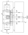
- FIG. 2 shows by a block diagram a capacity weight filter according to the invention. Elements identical to the elements already presented in the other figures bear the same references.
- the capacity weight filter according to the invention comprises at least two physically distinct cards: a motherboard 10 and a daughter card 30.
- the management and control card 2 can either have its functions integrated on the motherboard 10 or constitute a third map physically distinct from the other two.
- the management and control card 2 comprises all the elements participating in the control and servocontrol functions of the capacity weights A ... H.
- the daughter card 30 comprises all the elements participating in the towable filtering. , that is to say in particular the capacity weights A ... H.
- the daughter board 30 does not include any inductive element necessary for electromagnetic coupling.
- the daughter card 30 retains the symmetry of the elements participating in the towable filtering.
- the motherboard 10 comprises all the oscillating circuits.
- the interface between the motherboard 10 and the daughter board 30 is provided by a connector 31 and a wiring for the radio frequency signals 32 (shown in Figure 3).
- the connector 31 makes it possible, in particular, to transmit the commands originating from the card of management and control 2 to the daughter card 30, the motherboard 10 providing the routing of the signals to the connector 31.
- the wiring 32 makes it possible to pass to the daughter card 30 the radio frequency signals received on the input E of the motherboard 10, and reciprocally to the daughter card 30 to deliver filtered radio frequency signals to the motherboard 10 which will route them to the output S.
- the motherboard 10 has a zone 15 on which are arranged the inductive elements particularly necessary for the electromagnetic coupling of the oscillating circuits included on the daughter board 30.
- FIG. 3 shows schematic views of an exemplary embodiment of a capacity weight filter according to the invention. Elements identical to the elements already presented in the other figures bear the same references.
- the daughter board 30 and the motherboard 10 are boards manufactured in CMS (Surface Mounted Components) technology.
- the daughter card 30 may be a double-sided card, making it possible to reduce the area required for the elements of the towable filter.
- the daughter card 30 is disposed substantially orthogonal to the motherboard 10.
- the daughter card 30 may include pins, notches or other locking element disposed on the lower part in contact with the motherboard 10, the elements of blockages being introduced into notches facing each other on the motherboard 10.
- the connector 31 is a CMS connector.
- the wiring 32 may be achieved in particular by the end of the inductor using self-tap.
- the wiring 32 may also be made in particular using coaxial cables.
- series inductors are arranged on the motherboard 10 on the zone 15 to ensure the electromagnetic coupling of the oscillating circuits included on the daughter card 30. This choice makes it possible in particular to simplify the mechanical assembly of the daughter card 30 on the card mother 10. The choice of series inductors still makes it possible to operate the filter with constant Q quality.
- silver wire air inductors can be used.
- the manual wiring of the filter is limited mainly to the welding of the silver wire air inductors on the motherboard 10.
- the motherboard 10 may furthermore, if necessary, be associated with several daughterboards 30.
- a weld bead after assembly of the daughter board 30 and the main board is laid, thereby ensuring optimum mass return.
- the two oscillating circuits operate at critical coupling, a characteristic that can be determined from, in particular, the overvoltage coefficients of the inductors included in each oscillating circuit.
Landscapes
- Transceivers (AREA)
- Filters And Equalizers (AREA)
- Combinations Of Printed Boards (AREA)
Abstract
Description
- L'invention concerne un filtre agile de puissance compact. En particulier, l'invention s'applique au filtre de puissance compris dans un module d'amplification de système de radiocommunication. Par exemple, l'invention peut être utilisée par un système de radiocommunication programmable par voie logiciel s'adaptant à une gamme de signaux s'étendant sur une large plage de fréquences (dont l'étendue couvre plusieurs gigahertz). Ces modules dit logiciel peuvent encore s'adapter plus généralement à de nombreuses formes d'onde.
- Les systèmes de radiocommunications comportent généralement un module amplificateur, connecté entre d'une part un module radiofréquences et d'autre part un système antennaire. La fonction d'un tel module est d'amplifier le signal utile en émission comme en réception. Plus particulièrement, le signal utile amplifié transmis via le système antennaire doit être suffisamment puissant pour atteindre la portée voulue, occupé par une bande de fréquence correspondant à la forme d'onde employée pour atteindre les performances notamment en débit souhaité, tout en respectant les contraintes normatives et réglementaires imposées.
- Un module amplificateur se décompose principalement en dispositifs d'amplification de puissance du signal et en dispositifs de filtrage du signal utile. Les dispositifs de filtrage doivent s'adapter à des signaux utiles dont la forme d'onde occupe une bande passante particulièrement importante. A titre d'exemple, les systèmes logiciels de radiocommunications employant des formes d'ondes à évasion de fréquence peuvent émettre et/ou recevoir dans une plage de fréquences allant de 30 MHz à 3 GHz (soit la bande de fréquences couramment désignée par l'acronyme anglo-saxon VHF pour Very High Frequency et la bande de fréquences couramment désignée par l'acronyme anglo-saxon UHF pour Ultra High Frequency). Les dispositifs de filtrage doivent en conséquence garantir un fonctionnement compatible des formes d'ondes à évasion de fréquences, à savoir une compatibilité de la vitesse d'accord et une maîtrise du spectre émis. Les filtres dit filtres agiles permettent en particulier de répondre à cette problématique. Parmi les filtres agiles, on peut citer les filtres à poids de capacité encore appelé filtres tractables.
- La figure 1 montre, par un synoptique, un filtre à poids de capacité selon l'état de la technique. Le filtre comprend une carte principale 1. La carte principale 1 comporte une entée E par laquelle un signal à filtrer est reçu, et une sortie S sur laquelle un signal filtré est délivré. La carte principale 1 comprend deux circuits oscillants couplés magnétiquement. La carte principale 1 comporte encore des poids de capacité (sur la figure 1, 8 poids de capacité pour chaque circuit oscillant désignés par les lettres A à H). Le nombre de poids de capacité est lié à l'étendue de la bande de fréquence couverte par filtre ainsi que la bande de fréquence intrinsèque dudit filtre. Chaque poids de capacité A..H comporte sur la figure 1 une capacité et une diode. Chaque poids de capacité est commadé par des signaux reçus d'une carte de gestion et de contrôle 2. La carte de gestion et de contrôle 2 transforme les commandes qu'elle reçoit sur des entrées CA...CH en commandes pour les poids de capacités A..H. La carte de gestion et de contrôle 2 et la carte principale 1 sont généralement réalisé sur deux cartes électroniques distinctes interconnectées.
- Les filtres à poids de capacité selon l'état de la technique permettent de filtrer des signaux puissants (par exemple de l'ordre de 50W), en étant agile, sélectif et limitant les pertes. Néanmoins, l'encombrement de tels filtres est problématique. Il est possible de limiter l'encombrement d'un tel filtre par l'emploi de technique de montage à 3 dimensions. Néanmoins, ce contournement induit alors un surcoût conséquent. En effet, la conception d'un tel filtre est rendue plus complexe, les procédés de fabrication plus coûteux (la fabrication et le montage étant alors au moins en partie réalisée manuellement), et la mise au point sinon délicate au moins peu reproductible d'un filtre à l'autre. Plus généralement, le problème posé est celui de la miniaturisation de ce type de filtre dans un environnement industriel automatisé sans dégrader les performances techniques d'un tel filtre.
- L'invention a notamment pour but de pallier les inconvénients précités. A cet effet, l'invention a pour objet un filtre à poids de capacité comprenant deux circuits oscillants couplés électromagnétiquement. Chaque circuit oscillant comporte des poids de capacité. Chaque poids de capacité est commandé par des signaux. Le filtre comporte au moins une carte mère et une carte fille physiquement distinctes. La carte fille comporte les poids de capacité, la carte mère comporte l'ensemble des circuits oscillants.
- Dans un mode de réalisation, l'interface entre la carte mère et la carte fille est assurée par un connecteur et un câblage pour les signaux radiofréquences. Le connecteur permet de faire transiter les commandes destinées au poids de capacité. Le câblage permet de faire transiter jusqu'à la carte fille des signaux radiofréquences reçus par la carte mère. Le câblage permet de faire transiter de la carte fille les signaux radiofréquences filtrés. Le câblage peut être réalisé par l'extrémité de l'inductance à l'aide de selfs à prise. Des inductances en série peuvent être disposées sur la carte mère sur une zone assurant le couplage magnétique des circuits oscillants dont la partie capacitive est compris sur la carte fille. Les inductances peuvent par exemple être des inductances à air en fil argenté.
- Avantageusement, la carte fille est disposée de manière sensiblement orthogonale à la carte mère. En outre, la carte fille peut comporter des éléments de blocage disposés sur la partie basse en contact avec la carte mère, les éléments de blocages étant introduits dans des encoches en vis-à-vis disposé sur la carte mère.
- La carte fille, la carte mère, le connecteur peuvent être fabriquées en technologie Composants Montés en Surface. La carte fille peut être une carte double face.
- Dans un mode de réalisation, la carte mère est associée à plusieurs cartes filles.
- L'invention a notamment pour avantages qu'elle permet de garantir une sélectivité compatible des exigences techniques, normatives, réglementaire en terme de cosite, tout en conservant les notions de puissance et de faible encombrement. L'invention est en outre en cohérence avec les procédés de fabrication automatique mis en oeuvre aujourd'hui, comme par exemple les lignes de production dite « Composants Montés en Surface ».
- D'autres caractéristiques et avantages de l'invention apparaîtront à l'aide de la description qui suit faite en regard des dessins annexés qui représentent :
- la figure 1, un synoptique d'un filtre à poids de capacité selon l'état de la technique ;
- la figure 2, un synoptique d'un filtre à poids de capacité selon l'invention ;
- la figure 3, des vues schématiques d'un exemple de réalisation d'un filtre à poids de capacité selon l'invention.
- La figure 2 montre par un synoptique un filtre à poids de capacité selon l'invention. Les éléments identiques aux éléments déjà présentés sur les autres figures portent les mêmes références. Le filtre à poids de capacité selon l'invention comporte au moins deux cartes physiquement distinctes : une carte mère 10 et une carte fille 30. La carte de gestion et de contrôle 2 peut soit voir ses fonctions être intégrées sur la carte mère 10 soit constituer une troisième carte physiquement distincte des deux autres. La carte de gestion et de contrôle 2 regroupe l'ensemble des éléments participant aux fonctions de commande et d'asservissement des poids de capacité A... H. La carte fille 30 comporte quant à elle l'ensemble des éléments participant au filtrage tractable, c'est-à-dire notamment les poids de capacité A...H. La carte fille 30 ne comporte aucun élément inductif nécessaire au couplage électromagnétique. La carte fille 30 conserve la symétrie des éléments participants au filtrage tractable. La carte mère 10 comporte quant à elle l'ensemble des circuits oscillants. L'interface entre la carte mère 10 et la carte fille 30 est réalisée par un connecteur 31 et un câblage pour les signaux radiofréquences 32 (représentés à la figure 3). Le connecteur 31 permet notamment de faire transiter les commandes provenant de la carte de gestion et de contrôle 2 jusqu'à la carte fille 30, la carte mère 10 assurant le routage des signaux jusqu'au connecteur 31. Le câblage 32 permet de faire transiter jusqu'à la carte fille 30 les signaux radiofréquences reçus sur l'entrée E de la carte mère 10, et réciproquement à la carte fille 30 de délivrer des signaux radiofréquences filtrés vers la carte mère 10 qui les routera jusqu'à la sortie S. La carte mère 10 comporte une zone 15 sur laquelle sont disposés les éléments inductifs nécessaires notamment au couplage électromagnétique des circuits oscillants compris sur la carte fille 30.
- La figure 3 montre des vues schématiques d'un exemple de réalisation d'un filtre à poids de capacité selon l'invention. Les éléments identiques aux éléments déjà présentés sur les autres figures portent les mêmes références. La carte fille 30 et la carte mère 10 sont des cartes fabriquées en technologie CMS (CMS pour Composants Montés en Surface). La carte fille 30 peut être une carte double face, permettant de réduire la surface nécessaire aux éléments du filtre tractable. La carte fille 30 est disposée de manière sensiblement orthogonale à la carte mère 10. La carte fille 30 peut notamment comporter des picots, des encoches ou tout autre élément de blocage disposé sur la partie basse en contact avec la carte mère 10, les éléments de blocages étant introduits dans des encoches en vis-à-vis disposé sur la carte mère 10.
Le connecteur 31 est un connecteur CMS. Le câblage 32 peut être réalisé notamment par l'extrémité de l'inductance à l'aide de self à prise. Le câblage 32 peut être aussi réalisé notamment à l'aide de câble coaxiaux. En outre, des inductances en série sont disposées sur la carte mère 10 sur la zone 15 pour assurer le couplage électromagnétique des circuits oscillants compris sur la carte fille 30. Ce choix permet notamment de simplifier le montage mécanique de la carte fille 30 sur la carte mère 10. Le choix des inductances série permet encore de faire fonctionner le filtre à qualité Q constante. En particulier, des inductances à air en fil argenté peuvent être utilisées. Ainsi, le câblage manuel du filtre se limite principalement au soudage des inductances à air en fil argenté sur la carte mère 10. La carte mère 10 peut en outre si nécessaire être associée à plusieurs cartes filles 30. - Dans un mode de réalisation, un cordon de soudure après assemblage de la carte fille 30 et de la carte principale est posé, permettant ainsi d'assurer un retour de masse optimale.
Dans un mode de réalisation, les deux circuits oscillants fonctionnent au couplage critique, caractéristique déterminable à partir notamment des coefficients de surtension des selfs comprises dans chaque circuit oscillant.
Claims (10)
- Filtre à poids de capacité comprenant deux circuits oscillants couplés électromagnétiquement, chaque circuit oscillant comportant des poids de capacité (A... H), chaque poids de capacité (A... H) étant commadé par des signaux caractérisé en ce qu'il comporte au moins une carte mère (10) et une carte fille (30) physiquement distinctes, la carte fille (30) comportant les poids de capacité (A...H), la carte mère (10) comportant l'ensemble des circuits oscillants.
- Filtre à poids de capacité selon la revendication 1 caractérisé en ce que l'interface entre la carte mère (10) et la carte fille (30) est assurée par un connecteur (31) et un câblage pour les signaux radiofréquences (32), le connecteur (31) permettant de faire transiter les commandes destinées au poids de capacité (A...H), le câblage (32) permettant de faire transiter jusqu'à la carte fille (30) des signaux radiofréquences reçus par la carte mère (10), le câblage (32) permettant de faire transiter de la carte fille (30) les signaux radiofréquences filtrés.
- Filtre à poids de capacité selon l'une des quelconques revendications 1 à 2 caractérisé en ce que le câblage (32) est réalisé par l'extrémité de l'inductance à l'aide de self à prise.
- Filtre à poids de capacité selon l'une des quelconques revendications 1 à 3 caractérisé en ce que des inductances en série sont disposées sur la carte mère (10) sur une zone (15) assurant le couplage magnétique des circuits oscillants dont la partie capacitive est comprise sur la carte fille (30).
- Filtre à poids de capacité selon la revendication 4 caractérisé en ce que les inductances sont des inductances à air en fil argenté.
- Filtre à poids de capacité selon l'une des quelconques revendications 1 à 5 caractérisé en ce que la carte fille (30) est disposée de manière sensiblement orthogonale à la carte mère (30).
- Filtre à poids de capacité selon la revendication 6 caractérisé en ce que la carte fille (30) comporte des éléments de blocage disposés sur la partie basse en contact avec la carte mère (10), les éléments de blocages étant introduits dans des encoches en vis-à-vis disposé sur la carte mère (10).
- Filtre à poids de capacité selon l'une des quelconques revendications 1 à 7 caractérisé en ce que la carte fille (30), la carte mère (10), le connecteur (31) sont fabriquées en technologie Composants Montés en Surface.
- Filtre à poids de capacité selon l'une des quelconques revendications 1 à 8 caractérisé en ce que la carte fille (30) est une carte double face.
- Filtre à poids de capacité selon l'une des quelconques revendications 1 à 9 caractérisé en ce que la carte mère (10) est associée à plusieurs cartes filles (30).
Applications Claiming Priority (1)
| Application Number | Priority Date | Filing Date | Title |
|---|---|---|---|
| FR0608477A FR2906420B1 (fr) | 2006-09-27 | 2006-09-27 | Filtre agile de puissance compact, notamment pour module d'amplification de systeme de radiocommunication. |
Publications (2)
| Publication Number | Publication Date |
|---|---|
| EP1914889A1 true EP1914889A1 (fr) | 2008-04-23 |
| EP1914889B1 EP1914889B1 (fr) | 2014-09-03 |
Family
ID=37969972
Family Applications (1)
| Application Number | Title | Priority Date | Filing Date |
|---|---|---|---|
| EP07117431.2A Not-in-force EP1914889B1 (fr) | 2006-09-27 | 2007-09-27 | Filtre agile de puissance compact, notamment pour module d'amplification de système de radiocommunication |
Country Status (3)
| Country | Link |
|---|---|
| US (1) | US7812690B2 (fr) |
| EP (1) | EP1914889B1 (fr) |
| FR (1) | FR2906420B1 (fr) |
Family Cites Families (17)
| Publication number | Priority date | Publication date | Assignee | Title |
|---|---|---|---|---|
| US5625325A (en) * | 1995-12-22 | 1997-04-29 | Microtune, Inc. | System and method for phase lock loop gain stabilization |
| US5905398A (en) * | 1997-04-08 | 1999-05-18 | Burr-Brown Corporation | Capacitor array having user-adjustable, manufacturer-trimmable capacitance and method |
| US6327463B1 (en) * | 1998-05-29 | 2001-12-04 | Silicon Laboratories, Inc. | Method and apparatus for generating a variable capacitance for synthesizing high-frequency signals for wireless communications |
| US6150901A (en) * | 1998-11-20 | 2000-11-21 | Rockwell Collins, Inc. | Programmable RF/IF bandpass filter utilizing MEM devices |
| US6211745B1 (en) * | 1999-05-03 | 2001-04-03 | Silicon Wave, Inc. | Method and apparatus for digitally controlling the capacitance of an integrated circuit device using mos-field effect transistors |
| JP3820843B2 (ja) * | 1999-05-12 | 2006-09-13 | 株式会社日立製作所 | 方向性結合式メモリモジュール |
| US6535075B2 (en) * | 1999-12-16 | 2003-03-18 | International Business Machines Corporation | Tunable on-chip capacity |
| US6388532B1 (en) * | 2000-02-15 | 2002-05-14 | Cardinal Components, Inc. | System and method for programming oscillators |
| EP1143606B1 (fr) * | 2000-03-31 | 2003-11-19 | Texas Instruments Incorporated | Oscillateur variable commandé numériquement |
| DE10016974A1 (de) * | 2000-04-06 | 2001-10-11 | Philips Corp Intellectual Pty | Spule für automatisierte Montage |
| EP1189347A1 (fr) * | 2000-09-15 | 2002-03-20 | Texas Instruments France | Oscillateur commandé par une tension ajusté électroniquement |
| US6778022B1 (en) * | 2001-05-17 | 2004-08-17 | Rf Micro Devices, Inc. | VCO with high-Q switching capacitor bank |
| US20030132809A1 (en) * | 2002-01-17 | 2003-07-17 | Chinnugounder Senthilkumar | Oscillator with tunable capacitor |
| US7230503B1 (en) * | 2002-02-28 | 2007-06-12 | Silicon Laboratories Inc. | Imbalanced differential circuit control |
| US6882245B2 (en) * | 2002-06-05 | 2005-04-19 | Rf Stream Corporation | Frequency discrete LC filter bank |
| US6940365B2 (en) * | 2003-07-18 | 2005-09-06 | Rfstream Corporation | Methods and apparatus for an improved discrete LC filter |
| KR100548130B1 (ko) * | 2004-02-21 | 2006-02-02 | 삼성전자주식회사 | 광대역 튜너블 대역통과필터 및 이를 이용한 다중밴드광대역 튜너블 대역통과필터 |
-
2006
- 2006-09-27 FR FR0608477A patent/FR2906420B1/fr not_active Expired - Fee Related
-
2007
- 2007-09-27 EP EP07117431.2A patent/EP1914889B1/fr not_active Not-in-force
- 2007-09-27 US US11/862,988 patent/US7812690B2/en not_active Expired - Fee Related
Non-Patent Citations (2)
| Title |
|---|
| ENTESARI K ET AL: "A DIFFERENTIAL 4-BIT 6.5-10-GHZ RF MEMS TUNABLE FILTER", IEEE TRANSACTIONS ON MICROWAVE THEORY AND TECHNIQUES, IEEE SERVICE CENTER, PISCATAWAY, NJ, US, vol. 53, no. 3, PART 2, March 2005 (2005-03-01), pages 1103 - 1110, XP001225632, ISSN: 0018-9480 * |
| PETERSON D A: "GaAs insertion enhances SINCGARS RF preselector", TACTICAL COMMUNICATIONS CONFERENCE, 1992. VOL. 1 TACTICAL COMMUNICATIONS: TECHNOLOGY IN TRANSITION., PROCEEDINGS OF THE FORT WAYNE, IN, USA 28-30 APRIL 1992, NEW YORK, NY, USA,IEEE, US, 28 April 1992 (1992-04-28), pages 133 - 137, XP010066443, ISBN: 0-7803-0745-3 * |
Also Published As
| Publication number | Publication date |
|---|---|
| FR2906420B1 (fr) | 2008-11-21 |
| EP1914889B1 (fr) | 2014-09-03 |
| US7812690B2 (en) | 2010-10-12 |
| US20080174388A1 (en) | 2008-07-24 |
| FR2906420A1 (fr) | 2008-03-28 |
Similar Documents
| Publication | Publication Date | Title |
|---|---|---|
| US7760045B2 (en) | Semiconductor device interconnecting unit, semiconductor device, high-frequency module, and semiconductor device interconnecting method | |
| CN101075695B (zh) | 半导体装置互连单元、半导体装置以及高频模块 | |
| US7339445B2 (en) | BAW duplexer without phase shifter | |
| US20100188167A1 (en) | Ku-band diplexer | |
| WO2012039119A1 (fr) | Filtre de bruit | |
| US20090153263A1 (en) | Modulized wave filter | |
| EP2074700B1 (fr) | Module d'emission et de reception radioelectrique, adapte notamment aux radiocommunications large bande | |
| CN107039737A (zh) | 用于定向耦合器的无源均衡器 | |
| US7795996B2 (en) | Multilayered coplanar waveguide filter unit and method of manufacturing the same | |
| EP1914889B1 (fr) | Filtre agile de puissance compact, notamment pour module d'amplification de système de radiocommunication | |
| JPH08191230A (ja) | 分波器 | |
| EP1119101A1 (fr) | Circuit d'entrée pour dispositif d'accord pour récepteur de diffusion par satellite | |
| KR102433343B1 (ko) | 필터 간극 고정형 유전체 및 rf 필터가 구비된 rf 커넥터 | |
| US10454148B2 (en) | Compact band pass filter | |
| TWI730239B (zh) | 通訊模組 | |
| JP2006332980A (ja) | トリプレクサ回路 | |
| US20190372545A1 (en) | Compact band pass filter with vias | |
| KR102433339B1 (ko) | Rf 필터가 내장된 융합형 rf 커넥터 어댑터 및 이를 이용한 rf 송수신채널 어셈블리 | |
| JP2006180519A (ja) | ハイブリッド接続器及びその中継システム | |
| JP7811521B2 (ja) | 信号処理デバイス | |
| EP2744311A1 (fr) | Procede de realisation de motifs resonnants adaptes a la realisation de fonctions passives RF | |
| KR101014130B1 (ko) | 통합 안테나 시스템 | |
| EP2792016A1 (fr) | Circuit de transition ligne microruban/ligne fente | |
| KR20050095493A (ko) | 프론트 엔드 모듈의 쏘 필터 출력 라인 구조 | |
| WO2011117053A1 (fr) | Module frontal et procédé de fonctionnement dudit module frontal dans différents environnements de circuit |
Legal Events
| Date | Code | Title | Description |
|---|---|---|---|
| PUAI | Public reference made under article 153(3) epc to a published international application that has entered the european phase |
Free format text: ORIGINAL CODE: 0009012 |
|
| AK | Designated contracting states |
Kind code of ref document: A1 Designated state(s): AT BE BG CH CY CZ DE DK EE ES FI FR GB GR HU IE IS IT LI LT LU LV MC MT NL PL PT RO SE SI SK TR |
|
| AX | Request for extension of the european patent |
Extension state: AL BA HR MK RS |
|
| 17P | Request for examination filed |
Effective date: 20081023 |
|
| 17Q | First examination report despatched |
Effective date: 20081124 |
|
| AKX | Designation fees paid |
Designated state(s): AT BE BG CH CY CZ DE DK EE ES FI FR GB GR HU IE IS IT LI LT LU LV MC MT NL PL PT RO SE SI SK TR |
|
| GRAP | Despatch of communication of intention to grant a patent |
Free format text: ORIGINAL CODE: EPIDOSNIGR1 |
|
| INTG | Intention to grant announced |
Effective date: 20140516 |
|
| GRAS | Grant fee paid |
Free format text: ORIGINAL CODE: EPIDOSNIGR3 |
|
| GRAA | (expected) grant |
Free format text: ORIGINAL CODE: 0009210 |
|
| AK | Designated contracting states |
Kind code of ref document: B1 Designated state(s): AT BE BG CH CY CZ DE DK EE ES FI FR GB GR HU IE IS IT LI LT LU LV MC MT NL PL PT RO SE SI SK TR |
|
| REG | Reference to a national code |
Ref country code: GB Ref legal event code: FG4D Free format text: NOT ENGLISH |
|
| REG | Reference to a national code |
Ref country code: CH Ref legal event code: EP Ref country code: AT Ref legal event code: REF Ref document number: 686053 Country of ref document: AT Kind code of ref document: T Effective date: 20140915 |
|
| REG | Reference to a national code |
Ref country code: IE Ref legal event code: FG4D Free format text: LANGUAGE OF EP DOCUMENT: FRENCH |
|
| REG | Reference to a national code |
Ref country code: DE Ref legal event code: R096 Ref document number: 602007038381 Country of ref document: DE Effective date: 20141016 |
|
| REG | Reference to a national code |
Ref country code: SE Ref legal event code: TRGR |
|
| REG | Reference to a national code |
Ref country code: AT Ref legal event code: MK05 Ref document number: 686053 Country of ref document: AT Kind code of ref document: T Effective date: 20140903 |
|
| PG25 | Lapsed in a contracting state [announced via postgrant information from national office to epo] |
Ref country code: FI Free format text: LAPSE BECAUSE OF FAILURE TO SUBMIT A TRANSLATION OF THE DESCRIPTION OR TO PAY THE FEE WITHIN THE PRESCRIBED TIME-LIMIT Effective date: 20140903 Ref country code: GR Free format text: LAPSE BECAUSE OF FAILURE TO SUBMIT A TRANSLATION OF THE DESCRIPTION OR TO PAY THE FEE WITHIN THE PRESCRIBED TIME-LIMIT Effective date: 20141204 Ref country code: LT Free format text: LAPSE BECAUSE OF FAILURE TO SUBMIT A TRANSLATION OF THE DESCRIPTION OR TO PAY THE FEE WITHIN THE PRESCRIBED TIME-LIMIT Effective date: 20140903 Ref country code: ES Free format text: LAPSE BECAUSE OF FAILURE TO SUBMIT A TRANSLATION OF THE DESCRIPTION OR TO PAY THE FEE WITHIN THE PRESCRIBED TIME-LIMIT Effective date: 20140903 |
|
| REG | Reference to a national code |
Ref country code: NL Ref legal event code: VDEP Effective date: 20140903 |
|
| REG | Reference to a national code |
Ref country code: LT Ref legal event code: MG4D |
|
| PG25 | Lapsed in a contracting state [announced via postgrant information from national office to epo] |
Ref country code: CY Free format text: LAPSE BECAUSE OF FAILURE TO SUBMIT A TRANSLATION OF THE DESCRIPTION OR TO PAY THE FEE WITHIN THE PRESCRIBED TIME-LIMIT Effective date: 20140903 Ref country code: AT Free format text: LAPSE BECAUSE OF FAILURE TO SUBMIT A TRANSLATION OF THE DESCRIPTION OR TO PAY THE FEE WITHIN THE PRESCRIBED TIME-LIMIT Effective date: 20140903 Ref country code: LV Free format text: LAPSE BECAUSE OF FAILURE TO SUBMIT A TRANSLATION OF THE DESCRIPTION OR TO PAY THE FEE WITHIN THE PRESCRIBED TIME-LIMIT Effective date: 20140903 |
|
| PG25 | Lapsed in a contracting state [announced via postgrant information from national office to epo] |
Ref country code: NL Free format text: LAPSE BECAUSE OF FAILURE TO SUBMIT A TRANSLATION OF THE DESCRIPTION OR TO PAY THE FEE WITHIN THE PRESCRIBED TIME-LIMIT Effective date: 20140903 |
|
| PG25 | Lapsed in a contracting state [announced via postgrant information from national office to epo] |
Ref country code: RO Free format text: LAPSE BECAUSE OF FAILURE TO SUBMIT A TRANSLATION OF THE DESCRIPTION OR TO PAY THE FEE WITHIN THE PRESCRIBED TIME-LIMIT Effective date: 20140903 Ref country code: EE Free format text: LAPSE BECAUSE OF FAILURE TO SUBMIT A TRANSLATION OF THE DESCRIPTION OR TO PAY THE FEE WITHIN THE PRESCRIBED TIME-LIMIT Effective date: 20140903 Ref country code: SK Free format text: LAPSE BECAUSE OF FAILURE TO SUBMIT A TRANSLATION OF THE DESCRIPTION OR TO PAY THE FEE WITHIN THE PRESCRIBED TIME-LIMIT Effective date: 20140903 Ref country code: IS Free format text: LAPSE BECAUSE OF FAILURE TO SUBMIT A TRANSLATION OF THE DESCRIPTION OR TO PAY THE FEE WITHIN THE PRESCRIBED TIME-LIMIT Effective date: 20150103 Ref country code: CZ Free format text: LAPSE BECAUSE OF FAILURE TO SUBMIT A TRANSLATION OF THE DESCRIPTION OR TO PAY THE FEE WITHIN THE PRESCRIBED TIME-LIMIT Effective date: 20140903 Ref country code: PT Free format text: LAPSE BECAUSE OF FAILURE TO SUBMIT A TRANSLATION OF THE DESCRIPTION OR TO PAY THE FEE WITHIN THE PRESCRIBED TIME-LIMIT Effective date: 20150105 |
|
| REG | Reference to a national code |
Ref country code: CH Ref legal event code: PL |
|
| PG25 | Lapsed in a contracting state [announced via postgrant information from national office to epo] |
Ref country code: PL Free format text: LAPSE BECAUSE OF FAILURE TO SUBMIT A TRANSLATION OF THE DESCRIPTION OR TO PAY THE FEE WITHIN THE PRESCRIBED TIME-LIMIT Effective date: 20140903 |
|
| REG | Reference to a national code |
Ref country code: DE Ref legal event code: R097 Ref document number: 602007038381 Country of ref document: DE |
|
| REG | Reference to a national code |
Ref country code: IE Ref legal event code: MM4A |
|
| PG25 | Lapsed in a contracting state [announced via postgrant information from national office to epo] |
Ref country code: BE Free format text: LAPSE BECAUSE OF NON-PAYMENT OF DUE FEES Effective date: 20140930 Ref country code: MC Free format text: LAPSE BECAUSE OF FAILURE TO SUBMIT A TRANSLATION OF THE DESCRIPTION OR TO PAY THE FEE WITHIN THE PRESCRIBED TIME-LIMIT Effective date: 20140903 |
|
| PLBE | No opposition filed within time limit |
Free format text: ORIGINAL CODE: 0009261 |
|
| STAA | Information on the status of an ep patent application or granted ep patent |
Free format text: STATUS: NO OPPOSITION FILED WITHIN TIME LIMIT |
|
| PG25 | Lapsed in a contracting state [announced via postgrant information from national office to epo] |
Ref country code: LI Free format text: LAPSE BECAUSE OF NON-PAYMENT OF DUE FEES Effective date: 20140930 Ref country code: CH Free format text: LAPSE BECAUSE OF NON-PAYMENT OF DUE FEES Effective date: 20140930 Ref country code: DK Free format text: LAPSE BECAUSE OF FAILURE TO SUBMIT A TRANSLATION OF THE DESCRIPTION OR TO PAY THE FEE WITHIN THE PRESCRIBED TIME-LIMIT Effective date: 20140903 |
|
| 26N | No opposition filed |
Effective date: 20150604 |
|
| PG25 | Lapsed in a contracting state [announced via postgrant information from national office to epo] |
Ref country code: IT Free format text: LAPSE BECAUSE OF FAILURE TO SUBMIT A TRANSLATION OF THE DESCRIPTION OR TO PAY THE FEE WITHIN THE PRESCRIBED TIME-LIMIT Effective date: 20140903 Ref country code: IE Free format text: LAPSE BECAUSE OF NON-PAYMENT OF DUE FEES Effective date: 20140927 |
|
| PG25 | Lapsed in a contracting state [announced via postgrant information from national office to epo] |
Ref country code: SI Free format text: LAPSE BECAUSE OF FAILURE TO SUBMIT A TRANSLATION OF THE DESCRIPTION OR TO PAY THE FEE WITHIN THE PRESCRIBED TIME-LIMIT Effective date: 20140903 |
|
| PG25 | Lapsed in a contracting state [announced via postgrant information from national office to epo] |
Ref country code: BG Free format text: LAPSE BECAUSE OF FAILURE TO SUBMIT A TRANSLATION OF THE DESCRIPTION OR TO PAY THE FEE WITHIN THE PRESCRIBED TIME-LIMIT Effective date: 20140903 |
|
| PG25 | Lapsed in a contracting state [announced via postgrant information from national office to epo] |
Ref country code: MT Free format text: LAPSE BECAUSE OF FAILURE TO SUBMIT A TRANSLATION OF THE DESCRIPTION OR TO PAY THE FEE WITHIN THE PRESCRIBED TIME-LIMIT Effective date: 20140903 |
|
| PG25 | Lapsed in a contracting state [announced via postgrant information from national office to epo] |
Ref country code: LU Free format text: LAPSE BECAUSE OF NON-PAYMENT OF DUE FEES Effective date: 20140927 Ref country code: TR Free format text: LAPSE BECAUSE OF FAILURE TO SUBMIT A TRANSLATION OF THE DESCRIPTION OR TO PAY THE FEE WITHIN THE PRESCRIBED TIME-LIMIT Effective date: 20140903 Ref country code: HU Free format text: LAPSE BECAUSE OF FAILURE TO SUBMIT A TRANSLATION OF THE DESCRIPTION OR TO PAY THE FEE WITHIN THE PRESCRIBED TIME-LIMIT; INVALID AB INITIO Effective date: 20070927 |
|
| REG | Reference to a national code |
Ref country code: FR Ref legal event code: PLFP Year of fee payment: 10 |
|
| REG | Reference to a national code |
Ref country code: FR Ref legal event code: PLFP Year of fee payment: 11 |
|
| PGFP | Annual fee paid to national office [announced via postgrant information from national office to epo] |
Ref country code: FR Payment date: 20170829 Year of fee payment: 11 Ref country code: GB Payment date: 20170920 Year of fee payment: 11 Ref country code: DE Payment date: 20170920 Year of fee payment: 11 |
|
| PGFP | Annual fee paid to national office [announced via postgrant information from national office to epo] |
Ref country code: SE Payment date: 20170912 Year of fee payment: 11 |
|
| REG | Reference to a national code |
Ref country code: DE Ref legal event code: R119 Ref document number: 602007038381 Country of ref document: DE |
|
| REG | Reference to a national code |
Ref country code: SE Ref legal event code: EUG |
|
| GBPC | Gb: european patent ceased through non-payment of renewal fee |
Effective date: 20180927 |
|
| PG25 | Lapsed in a contracting state [announced via postgrant information from national office to epo] |
Ref country code: SE Free format text: LAPSE BECAUSE OF NON-PAYMENT OF DUE FEES Effective date: 20180928 |
|
| PG25 | Lapsed in a contracting state [announced via postgrant information from national office to epo] |
Ref country code: DE Free format text: LAPSE BECAUSE OF NON-PAYMENT OF DUE FEES Effective date: 20190402 |
|
| PG25 | Lapsed in a contracting state [announced via postgrant information from national office to epo] |
Ref country code: FR Free format text: LAPSE BECAUSE OF NON-PAYMENT OF DUE FEES Effective date: 20180930 |
|
| PG25 | Lapsed in a contracting state [announced via postgrant information from national office to epo] |
Ref country code: GB Free format text: LAPSE BECAUSE OF NON-PAYMENT OF DUE FEES Effective date: 20180927 |