EP1914804A2 - Familie einzelner Footprints in integrierten Strommodulen - Google Patents
Familie einzelner Footprints in integrierten Strommodulen Download PDFInfo
- Publication number
- EP1914804A2 EP1914804A2 EP07012195A EP07012195A EP1914804A2 EP 1914804 A2 EP1914804 A2 EP 1914804A2 EP 07012195 A EP07012195 A EP 07012195A EP 07012195 A EP07012195 A EP 07012195A EP 1914804 A2 EP1914804 A2 EP 1914804A2
- Authority
- EP
- European Patent Office
- Prior art keywords
- power
- footprint
- power module
- module
- modules
- Prior art date
- Legal status (The legal status is an assumption and is not a legal conclusion. Google has not performed a legal analysis and makes no representation as to the accuracy of the status listed.)
- Withdrawn
Links
Images


Classifications
-
- H—ELECTRICITY
- H10—SEMICONDUCTOR DEVICES; ELECTRIC SOLID-STATE DEVICES NOT OTHERWISE PROVIDED FOR
- H10W—GENERIC PACKAGES, INTERCONNECTIONS, CONNECTORS OR OTHER CONSTRUCTIONAL DETAILS OF DEVICES COVERED BY CLASS H10
- H10W72/00—Interconnections or connectors in packages
-
- H—ELECTRICITY
- H05—ELECTRIC TECHNIQUES NOT OTHERWISE PROVIDED FOR
- H05K—PRINTED CIRCUITS; CASINGS OR CONSTRUCTIONAL DETAILS OF ELECTRIC APPARATUS; MANUFACTURE OF ASSEMBLAGES OF ELECTRICAL COMPONENTS
- H05K1/00—Printed circuits
- H05K1/02—Details
- H05K1/0286—Programmable, customizable or modifiable circuits
- H05K1/0295—Programmable, customizable or modifiable circuits adapted for choosing between different types or different locations of mounted components
-
- H—ELECTRICITY
- H05—ELECTRIC TECHNIQUES NOT OTHERWISE PROVIDED FOR
- H05K—PRINTED CIRCUITS; CASINGS OR CONSTRUCTIONAL DETAILS OF ELECTRIC APPARATUS; MANUFACTURE OF ASSEMBLAGES OF ELECTRICAL COMPONENTS
- H05K1/00—Printed circuits
- H05K1/18—Printed circuits structurally associated with non-printed electric components
- H05K1/181—Printed circuits structurally associated with non-printed electric components associated with surface mounted components
-
- H—ELECTRICITY
- H10—SEMICONDUCTOR DEVICES; ELECTRIC SOLID-STATE DEVICES NOT OTHERWISE PROVIDED FOR
- H10W—GENERIC PACKAGES, INTERCONNECTIONS, CONNECTORS OR OTHER CONSTRUCTIONAL DETAILS OF DEVICES COVERED BY CLASS H10
- H10W70/00—Package substrates; Interposers; Redistribution layers [RDL]
- H10W70/60—Insulating or insulated package substrates; Interposers; Redistribution layers
- H10W70/62—Insulating or insulated package substrates; Interposers; Redistribution layers characterised by their interconnections
- H10W70/65—Shapes or dispositions of interconnections
-
- H—ELECTRICITY
- H05—ELECTRIC TECHNIQUES NOT OTHERWISE PROVIDED FOR
- H05K—PRINTED CIRCUITS; CASINGS OR CONSTRUCTIONAL DETAILS OF ELECTRIC APPARATUS; MANUFACTURE OF ASSEMBLAGES OF ELECTRICAL COMPONENTS
- H05K2201/00—Indexing scheme relating to printed circuits covered by H05K1/00
- H05K2201/09—Shape and layout
- H05K2201/09818—Shape or layout details not covered by a single group of H05K2201/09009 - H05K2201/09809
- H05K2201/09954—More mounting possibilities, e.g. on same place of PCB, or by using different sets of edge pads
-
- H—ELECTRICITY
- H05—ELECTRIC TECHNIQUES NOT OTHERWISE PROVIDED FOR
- H05K—PRINTED CIRCUITS; CASINGS OR CONSTRUCTIONAL DETAILS OF ELECTRIC APPARATUS; MANUFACTURE OF ASSEMBLAGES OF ELECTRICAL COMPONENTS
- H05K2201/00—Indexing scheme relating to printed circuits covered by H05K1/00
- H05K2201/10—Details of components or other objects attached to or integrated in a printed circuit board
- H05K2201/10613—Details of electrical connections of non-printed components, e.g. special leads
- H05K2201/10621—Components characterised by their electrical contacts
- H05K2201/10689—Leaded Integrated Circuit [IC] package, e.g. dual-in-line [DIL]
-
- Y—GENERAL TAGGING OF NEW TECHNOLOGICAL DEVELOPMENTS; GENERAL TAGGING OF CROSS-SECTIONAL TECHNOLOGIES SPANNING OVER SEVERAL SECTIONS OF THE IPC; TECHNICAL SUBJECTS COVERED BY FORMER USPC CROSS-REFERENCE ART COLLECTIONS [XRACs] AND DIGESTS
- Y02—TECHNOLOGIES OR APPLICATIONS FOR MITIGATION OR ADAPTATION AGAINST CLIMATE CHANGE
- Y02P—CLIMATE CHANGE MITIGATION TECHNOLOGIES IN THE PRODUCTION OR PROCESSING OF GOODS
- Y02P70/00—Climate change mitigation technologies in the production process for final industrial or consumer products
- Y02P70/50—Manufacturing or production processes characterised by the final manufactured product
-
- Y—GENERAL TAGGING OF NEW TECHNOLOGICAL DEVELOPMENTS; GENERAL TAGGING OF CROSS-SECTIONAL TECHNOLOGIES SPANNING OVER SEVERAL SECTIONS OF THE IPC; TECHNICAL SUBJECTS COVERED BY FORMER USPC CROSS-REFERENCE ART COLLECTIONS [XRACs] AND DIGESTS
- Y10—TECHNICAL SUBJECTS COVERED BY FORMER USPC
- Y10T—TECHNICAL SUBJECTS COVERED BY FORMER US CLASSIFICATION
- Y10T29/00—Metal working
- Y10T29/49—Method of mechanical manufacture
- Y10T29/49002—Electrical device making
-
- Y—GENERAL TAGGING OF NEW TECHNOLOGICAL DEVELOPMENTS; GENERAL TAGGING OF CROSS-SECTIONAL TECHNOLOGIES SPANNING OVER SEVERAL SECTIONS OF THE IPC; TECHNICAL SUBJECTS COVERED BY FORMER USPC CROSS-REFERENCE ART COLLECTIONS [XRACs] AND DIGESTS
- Y10—TECHNICAL SUBJECTS COVERED BY FORMER USPC
- Y10T—TECHNICAL SUBJECTS COVERED BY FORMER US CLASSIFICATION
- Y10T29/00—Metal working
- Y10T29/49—Method of mechanical manufacture
- Y10T29/49002—Electrical device making
- Y10T29/4902—Electromagnet, transformer or inductor
-
- Y—GENERAL TAGGING OF NEW TECHNOLOGICAL DEVELOPMENTS; GENERAL TAGGING OF CROSS-SECTIONAL TECHNOLOGIES SPANNING OVER SEVERAL SECTIONS OF THE IPC; TECHNICAL SUBJECTS COVERED BY FORMER USPC CROSS-REFERENCE ART COLLECTIONS [XRACs] AND DIGESTS
- Y10—TECHNICAL SUBJECTS COVERED BY FORMER USPC
- Y10T—TECHNICAL SUBJECTS COVERED BY FORMER US CLASSIFICATION
- Y10T29/00—Metal working
- Y10T29/49—Method of mechanical manufacture
- Y10T29/49002—Electrical device making
- Y10T29/49117—Conductor or circuit manufacturing
- Y10T29/49124—On flat or curved insulated base, e.g., printed circuit, etc.
- Y10T29/4913—Assembling to base an electrical component, e.g., capacitor, etc.
-
- Y—GENERAL TAGGING OF NEW TECHNOLOGICAL DEVELOPMENTS; GENERAL TAGGING OF CROSS-SECTIONAL TECHNOLOGIES SPANNING OVER SEVERAL SECTIONS OF THE IPC; TECHNICAL SUBJECTS COVERED BY FORMER USPC CROSS-REFERENCE ART COLLECTIONS [XRACs] AND DIGESTS
- Y10—TECHNICAL SUBJECTS COVERED BY FORMER USPC
- Y10T—TECHNICAL SUBJECTS COVERED BY FORMER US CLASSIFICATION
- Y10T29/00—Metal working
- Y10T29/49—Method of mechanical manufacture
- Y10T29/49002—Electrical device making
- Y10T29/49117—Conductor or circuit manufacturing
- Y10T29/49124—On flat or curved insulated base, e.g., printed circuit, etc.
- Y10T29/4913—Assembling to base an electrical component, e.g., capacitor, etc.
- Y10T29/49133—Assembling to base an electrical component, e.g., capacitor, etc. with component orienting
- Y10T29/49137—Different components
Definitions
- the present invention relates generally to power modules and, more particularly, to a family of integrated power modules having a common footprint.
- FET field effect transistor
- a power module method comprises:
- FIG. 1 illustrates an embodiment of a power module.
- FIG. 2 illustrates on example of a power module having a single die.
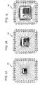
- FIGS. 3A-3C illustrate an example of a family of power modules.
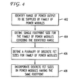
- FIG. 4 illustrates a flowchart of a process for defining a family of power modules.
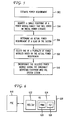
- FIG. 5 illustrates a flowchart of a design process that leverages a family of power modules.
- FIG. 6 illustrates a power over Ethernet example application.
- POL power module 100 includes integrated FETs in a two-phase design.
- PWM controller 110 is designed to control FETs 112, which in turn drive load 114
- PWM controller 120 is designed to control FETs 114, which in turn drive load 124.
- loads 114 and 124 can represent any type of system/subsystem that is powered off of the rail.
- loads 114 and 124 can represent communication system components such as a line card, mother board, etc.
- power module 100 is designed to drive two loads. As would be appreciated; power module 100 can be designed to deliver power to any number of loads, which are each designed to operate at a given voltage such as 0.6V, 0.9V, 1.OV, 1.1 V, 1.2V, 1.25V, 1.SV, 1.8V, 2.5V, 3.3V, 5.0V, etc.
- power module 100 can be designed to convert AC or DC input power to one of AC or DC output power. Further, power module 100 can be designed to include controllers other than PWM controllers. For example, power module 100 can also be designed with resonant mode controllers, hysteretic controllers, fuzzy logic controllers, or the like.
- the actual power drawn by a load is far less than the initial conservative power estimates. This results due to the risks associated with having a power module that is undersized for the finally designed load. If the initial power estimates prove to be too low, then the system designer would need to boost the capacity (i.e., size) of the FET, which would therefore lead to a complete relayout of the design. Conversely, if the initial power estimates prove to be too high, then the system designer could choose to reduce the capacity of the FET, which would also lead to a complete relayout of the design. As would be appreciated, in either case, the difficulties inherent in generating an initial power estimate for the load can lead to layout design changes late in the product development cycle.
- the present invention seeks to provide system designers with the flexibility in accommodating continual changes in power requirements during the design process. Indeed, it is a feature of the present invention that system designers can select a single power module for, a system design that has a footprint that is consistent across a range of power levels. In this process, the particular power level chosen for the power module can be specified later in the design process, wherein adjustments to the power requirements would not result in a change in the size of the overall power module.
- power module 200 includes a single die 210 that integrates the FETs 214 with the controller 212. This single die 210 is then coupled to pins 1-44 to produce power module 200.
- the power module could also be designed as a multi-chip module, wherein a plurality of dies are contained therein. This multi-chip module design would also enable the benefits of the present invention disclosed herein.
- pins 1-44 of power module 200 define a footprint that is used by system designers in the board layout that incorporates the power module. In conventional design processes, this footprint is generally proportional to the power capacity of the power module. Once a conservative power estimate is generated, the power module would then be designed to meet the needed power specifications. The footprint of the power module design would then be sized in accordance with the die that is incorporated within the power module: This footprint size would then be used in the board layout design. Since this footprint size is typically minimized with respect to the die contained within, a change in the size of the die would typically force a change in the footprint. As noted above, this change in footprint can produce a cascading series of changes in the board layout.
- the footprint of a power module is determined based on considerations other than the size of the die contained within. These additional considerations are focused on producing flexibility in the design process by eliminating the heavy dependence on conservative power estimates.
- FIGS. 3A-3C illustrate power modules 310 and 330, respectively.
- each of power modules 310, 320, and 330 house a single die, wherein each die has a different size.
- the variations in the size of the dies correspond to different power capacities for power modules 310, 320, 330.
- the footprint of each of power modules 310, 320, 330 is the same.
- power modules 310, 320, 330 represent a family of power modules that produce a range of power capacities for a given footprint.
- the range of power capacities for a given footprint can be defined to include any number of power modules.
- FIG. 4 illustrates a process for defining a family of power modules having a single footprint.
- the process begins at step 402 where a power module supplier identifies a range of power outputs to be supplied by a family of power modules.
- This range of power outputs can be defined in various ways. For example, the range of power outputs can be based on predefined power classes for a given application, de facto standards, or power module supplier considerations such as volume, manufacturing efficiencies, customer history, anticipated demand, etc.
- a single footprint size is selected to cover the power modules that span the range of power outputs:
- FIGS. 3A-3C illustrate one example of the single footprint size that is selected for the family of power modules 310, 320, and 330.
- the single footprint size can be selected as the minimum size that can accommodate the largest FET size needed to provide a power output at the top of the range of power outputs. This need not be a requirement, however.
- the single footprint size can be selected as any size that can accommodate the various FET sizes in that class.
- the range of power outputs is defined prior to the single footprint size. It should be noted that in an alternative embodiment, the single footprint size can be defined first, with the range of power outputs being defined based on the selection of the single footprint size.
- the key to providing a family of power modules is the defining, at step 406, of a plurality of discrete FET sizes for that family of power modules.
- these discrete FET sizes are predefined in incremental steps to cover the range of power outputs. This embodiment would enable a customer to select the FET having the next largest size that would satisfy the finally identified power requirement. Assuming that the incremental steps have a reasonable granularity, the customer would then be able to closely match the FET size to the finally identified power requirement.
- incremental FET sizes need not be predefined. Rather, a customer could choose to specify a specific FET size from a continuum of FET sizes that would fit within the single footprint size.
- step 408 discrete FET sizes are incorporated within power modules having the same footprint. Whether predefined incremental FET sizes are used or customer specific sizes are provided, multiple FET sizes are matched to power modules having the same footprint. The manufacturing of such a family of power modules is an important aspect of enabling needed flexibility in the design process.
- the design process begins at step 502 where an initial power estimate is determined.
- This initial power estimate can be determined using conventional system design methodologies. In accordance with the present invention, this initial power estimate need not be determined in an overly conservative manner. This results due to the known flexibility in the design process as described below.
- a footprint common to a family of power modules that will cover the initial power estimate is identified.
- this footprint can be determined based on data sheets provided by the power module supplier that cover a range of power outputs. This single footprint can then be used in the layout of a logic board.
- step 506 the actual power requirement of a load in the system is determined. As noted above, this actual power requirement may not be known until the actual circuit has been designed and tested. This occurs late in the design process.
- a single power module in a family of power modules having the identified footprint is selected.
- the single power module can be selected from a plurality of predefined power modules. The closeness of the match between the selected power modules to the actual power requirement would depend on the granularity of the differences between the plurality of predefined power modules.
- the power module can be specified based on the actual power requirement. Here, the power module could be determined to closely match the actual power requirement. In general, the difference between these two approaches could simply be one of time in providing the power module to the customer.
- the selected power module is incorporated into the originally identified footprint of the power modules in the system design.
- the originally identified footprint was not changed through the design process. Rather, the footprint was originally selected with the knowledge that it would cover expected differences between the actual power requirement and the initial power estimate. This flexibility therefore ensures that layout redesigns based on faulty power consumption estimates would be minimized.
- the system designer now has the ability to size up or down the capacity of the FET without concern for the costs of a relayout of the design.
- PoE power over Ethernet
- FIG. 6 illustrates a high-level overview of a PoE application that benefits from the principles of the present invention.
- a power source equipment (PSE) 610 is shown delivering power to a powered device (PD) 620.
- PSE 610 can deliver up to 15.4W of power to a plurality of PDs (only one PD is shown in FIG. 6 for simplicity). Details of the delivery of power from PSE 610 to PD 620 are provided in the IEEE 802.3af standard.
- PD 620 includes 802.3af module 622. This module includes the electronics that would enable PD 620 to communicate with PSE 610 in accordance with the 802.3af standard. PD 620 also includes power module 624, which further includes a PWM controller 626 and power FET 628. As noted above, PWM controller 626 and power FET 628 can be incorporated in a single die, or can be on separate dies as part of a multi-chip module.
- the PSE In the IEEE 802.3af standard, different classes of PDs are defined based on the power levels to be delivered at the PD. Once a PD is classified, the PSE would then determine which power level to deliver to the PD based on the determined classification. In the 802.3af standard, the PSE would be designed to deliver a minimum output power of.4.OW, 7.0W, or 15.4W to the classified PD.
- each power classification can be used to define its own family of power modules.
- the 4.0W power classification would have a first family of power modules and the 7.0W power classification would have a second family of power modules.
- PD designers could then design a layout that accommodates a power module having a footprint for the anticipated class of the device. The exact power module chosen would not need to be determined until the exact power requirement is known. Regardless of the power module chosen from the family, it would simply slot into the footprint defined for that family.
- family of power modules need not necessarily be defined based on the standardized power classifications. In other embodiments, a family of power modules can be defined to span all or part of one or more power classifications.
- the principles of the present invention can also be applied to modules within a PSE.
- the PSE could include a power module that contained the 802.3af circuitry along with a FET.
- multiple versions of the PSE power modules could be produced with FETs integrated inside the package.
- the 802.3af portion can be fixed but the internal FETs could be scaled for different power levels.
- a FET can be designed for 8W (low power), 15.4W (standard power), 25W (enhanced power), or 30W (future standard power).
- these integrated power modules can be used for single or multiport PSEs.
- a power controller would be used to provide on-off functionality for a FET that delivers power to an automotive subsystem (e.g., lights).
- an automotive subsystem e.g., lights
- a family of relays having a common footprint or other packaging characteristic could be defined.
- the system designer would then choose the particular relay from the family of relays. Again, this choice could be delayed until the actual power requirements are known, the last minute changes of which would not dictate system redesigns.
Landscapes
- Engineering & Computer Science (AREA)
- Microelectronics & Electronic Packaging (AREA)
- Direct Current Feeding And Distribution (AREA)
- Semiconductor Integrated Circuits (AREA)
- Design And Manufacture Of Integrated Circuits (AREA)
Applications Claiming Priority (1)
| Application Number | Priority Date | Filing Date | Title |
|---|---|---|---|
| US11/581,354 US7996987B2 (en) | 2006-10-17 | 2006-10-17 | Single footprint family of integrated power modules |
Publications (2)
| Publication Number | Publication Date |
|---|---|
| EP1914804A2 true EP1914804A2 (de) | 2008-04-23 |
| EP1914804A3 EP1914804A3 (de) | 2009-06-03 |
Family
ID=38984163
Family Applications (1)
| Application Number | Title | Priority Date | Filing Date |
|---|---|---|---|
| EP07012195A Withdrawn EP1914804A3 (de) | 2006-10-17 | 2007-06-21 | Familie einzelner Footprints in integrierten Strommodulen |
Country Status (5)
| Country | Link |
|---|---|
| US (1) | US7996987B2 (de) |
| EP (1) | EP1914804A3 (de) |
| KR (1) | KR100944114B1 (de) |
| CN (1) | CN101165892B (de) |
| TW (1) | TWI419293B (de) |
Families Citing this family (1)
| Publication number | Priority date | Publication date | Assignee | Title |
|---|---|---|---|---|
| ITUB20155696A1 (it) | 2015-11-18 | 2017-05-18 | St Microelectronics Srl | Dispositivo a semiconduttore, corrispondenti procedimenti di produzione ed uso e corrispondente apparecchiatura |
Citations (2)
| Publication number | Priority date | Publication date | Assignee | Title |
|---|---|---|---|---|
| US5959845A (en) | 1997-09-18 | 1999-09-28 | International Business Machines Corporation | Universal chip carrier connector |
| US20040201094A1 (en) | 2003-04-11 | 2004-10-14 | Yusuke Sato | Semiconductor device |
Family Cites Families (31)
| Publication number | Priority date | Publication date | Assignee | Title |
|---|---|---|---|---|
| US4489365A (en) * | 1982-09-17 | 1984-12-18 | Burroughs Corporation | Universal leadless chip carrier mounting pad |
| JPH07114279B2 (ja) * | 1988-01-06 | 1995-12-06 | 株式会社東芝 | 半導体装置 |
| US4965710A (en) * | 1989-11-16 | 1990-10-23 | International Rectifier Corporation | Insulated gate bipolar transistor power module |
| US6952705B2 (en) * | 1997-03-25 | 2005-10-04 | Mci, Inc. | Method, system and program product that utilize a hierarchical conceptual framework to model an environment containing a collection of items |
| DE69832359T2 (de) * | 1997-07-19 | 2006-08-03 | Koninklijke Philips Electronics N.V. | Halbleitervorrichtung -anordnung und -schaltungen |
| US5994965A (en) | 1998-04-03 | 1999-11-30 | Cbs Corporation | Silicon carbide high frequency high power amplifier |
| US6740969B1 (en) * | 1999-08-25 | 2004-05-25 | Renesas Technology Corp. | Electronic device |
| US6310783B1 (en) * | 2000-03-29 | 2001-10-30 | Powerware Corporation | Modular method and apparatus for building an uninterruptible power system (UPS) |
| US6496383B1 (en) * | 2000-08-09 | 2002-12-17 | Advanced Micro Devices, Inc. | Integrated circuit carrier arrangement for reducing non-uniformity in current flow through power pins |
| DE10102621B4 (de) * | 2001-01-20 | 2006-05-24 | Conti Temic Microelectronic Gmbh | Leistungsmodul |
| US20040245969A1 (en) * | 2001-06-18 | 2004-12-09 | Mcclean Joseph | Power converters |
| US6774465B2 (en) * | 2001-10-05 | 2004-08-10 | Fairchild Korea Semiconductor, Ltd. | Semiconductor power package module |
| US20040168818A1 (en) * | 2002-01-17 | 2004-09-02 | Powerware Corporation | System for detecting defective battery packs |
| US6686726B1 (en) * | 2002-08-08 | 2004-02-03 | Innoveta Technologies, Inc. | Tracking or independent output voltage adjustment for multiple output supplies |
| US7285973B1 (en) * | 2002-10-03 | 2007-10-23 | Xilinx, Inc. | Methods for standardizing a test head assembly |
| US7187562B2 (en) * | 2002-11-11 | 2007-03-06 | International Rectifier Corporation | Two stage power conversion circuit |
| US7088004B2 (en) * | 2002-11-27 | 2006-08-08 | International Rectifier Corporation | Flip-chip device having conductive connectors |
| US6798295B2 (en) * | 2002-12-13 | 2004-09-28 | Cree Microwave, Inc. | Single package multi-chip RF power amplifier |
| JP2004253706A (ja) * | 2003-02-21 | 2004-09-09 | Seiko Epson Corp | リードフレーム、半導体チップのパッケージング部材、半導体装置の製造方法、及び、半導体装置 |
| DE10320579A1 (de) * | 2003-05-07 | 2004-08-26 | Infineon Technologies Ag | Halbleiterwafer, Nutzen und elektronisches Bauteil mit gestapelten Halbleiterchips, sowie Verfahren zur Herstellung derselben |
| US7304263B2 (en) * | 2003-08-14 | 2007-12-04 | Rapt Industries, Inc. | Systems and methods utilizing an aperture with a reactive atom plasma torch |
| US7086019B2 (en) * | 2003-08-25 | 2006-08-01 | Hewlett-Packard Development Company, L.P. | Systems and methods for determining activity factors of a circuit design |
| FR2860932B1 (fr) * | 2003-10-10 | 2006-01-27 | Cit Alcatel | Carte de connexion ethernet a un reseau local, a controle de raccordement a un terminal de communication |
| US7345361B2 (en) * | 2003-12-04 | 2008-03-18 | Intel Corporation | Stackable integrated circuit packaging |
| US6982574B2 (en) * | 2004-03-22 | 2006-01-03 | Semiconductor Components Industries, Llc | Method of forming a transistor driver and structure therefor |
| US7363525B2 (en) * | 2004-10-07 | 2008-04-22 | Cisco Technology, Inc. | Bidirectional inline power port |
| US7555665B2 (en) * | 2004-12-29 | 2009-06-30 | Hewlett-Packard Development Company, L.P. | Method and apparatus of disabling converters in a power module |
| US7256479B2 (en) * | 2005-01-13 | 2007-08-14 | Fairchild Semiconductor Corporation | Method to manufacture a universal footprint for a package with exposed chip |
| US7479876B2 (en) * | 2005-02-02 | 2009-01-20 | Rockwell Automation Technologies, Inc. | Wireless integrated condition monitoring system |
| US20060220191A1 (en) * | 2005-04-01 | 2006-10-05 | Honeywell International Inc. | Electronic package with a stepped-pitch leadframe |
| US20070023889A1 (en) * | 2005-08-01 | 2007-02-01 | Salmon Peter C | Copper substrate with feedthroughs and interconnection circuits |
-
2006
- 2006-10-17 US US11/581,354 patent/US7996987B2/en not_active Expired - Fee Related
-
2007
- 2007-06-21 EP EP07012195A patent/EP1914804A3/de not_active Withdrawn
- 2007-10-15 KR KR1020070103484A patent/KR100944114B1/ko not_active Expired - Fee Related
- 2007-10-16 CN CN200710181388XA patent/CN101165892B/zh not_active Expired - Fee Related
- 2007-10-17 TW TW096138843A patent/TWI419293B/zh not_active IP Right Cessation
Patent Citations (2)
| Publication number | Priority date | Publication date | Assignee | Title |
|---|---|---|---|---|
| US5959845A (en) | 1997-09-18 | 1999-09-28 | International Business Machines Corporation | Universal chip carrier connector |
| US20040201094A1 (en) | 2003-04-11 | 2004-10-14 | Yusuke Sato | Semiconductor device |
Also Published As
| Publication number | Publication date |
|---|---|
| CN101165892A (zh) | 2008-04-23 |
| KR20080034785A (ko) | 2008-04-22 |
| HK1118951A1 (en) | 2009-02-20 |
| US20080086870A1 (en) | 2008-04-17 |
| US7996987B2 (en) | 2011-08-16 |
| KR100944114B1 (ko) | 2010-03-02 |
| TW200834861A (en) | 2008-08-16 |
| TWI419293B (zh) | 2013-12-11 |
| CN101165892B (zh) | 2011-03-23 |
| EP1914804A3 (de) | 2009-06-03 |
Similar Documents
| Publication | Publication Date | Title |
|---|---|---|
| CN103930848B (zh) | 用于电子设备的功率管理 | |
| US7380146B2 (en) | Power management system | |
| CN110165890B (zh) | 使用单个电感元件执行降压-升压转换的电子电路 | |
| CN1954284A (zh) | 集成电源系统 | |
| US12113442B2 (en) | Stacked buck converter with inductor switching node pre-charge and conduction modulation control | |
| CN100412760C (zh) | 用于基于通用串行总线的装置的节电系统和方法 | |
| CN101043212B (zh) | 半导体集成电路器件及其电路插入方法 | |
| JP2022097390A (ja) | 動的usb-cモード選択ospmポリシー方法及び装置 | |
| Sayani et al. | Analyzing and determining optimum on-board power architectures for 48 V-input systems | |
| US6681335B1 (en) | System for controlling power plane of a printed circuit board by using a single voltage regulator to control switches during first and second power modes | |
| US8250391B2 (en) | Method and system of improving memory power efficiency | |
| EP1914804A2 (de) | Familie einzelner Footprints in integrierten Strommodulen | |
| US20060015760A1 (en) | Semiconductor device for supplying power supply voltage to semiconductor device | |
| CN113687706B (zh) | 一种自动调整ncsi是否开启的装置和方法 | |
| US20250348121A1 (en) | Scalable, Hierarchical Power Delivery System | |
| CN207926553U (zh) | 一种多功能开关控制器 | |
| CN202713254U (zh) | 电子开关 | |
| CN101872997A (zh) | 连续提供电源的切换控制方法及其装置与电源供应系统 | |
| HK1118951B (en) | Single footprint family of integrated power modules | |
| Wang et al. | 3D reconfigurable power switch network for demand-supply matching between multi-output power converters and many-core microprocessors | |
| EP2610704A2 (de) | Integrierte Schaltung, adaptive Leistungsversorgung mit integrierten Schaltungseigenschaften und adaptives Leistungsversorgungsverfahren in Übereinstimmung mit den integrierten Schaltungseigenschaften, elektronische Vorrichtung damit und Verfahren zur Herstellung einer elektronischen Schaltung | |
| CN104281248A (zh) | 电压适配器 | |
| US20250038647A1 (en) | Scalable switch capacitor voltage regulators | |
| US20120307584A1 (en) | Memory power supply circuit | |
| Christiansen | Servers, workstations, personal computers: the looming power bottleneck |
Legal Events
| Date | Code | Title | Description |
|---|---|---|---|
| PUAI | Public reference made under article 153(3) epc to a published international application that has entered the european phase |
Free format text: ORIGINAL CODE: 0009012 |
|
| AK | Designated contracting states |
Kind code of ref document: A2 Designated state(s): AT BE BG CH CY CZ DE DK EE ES FI FR GB GR HU IE IS IT LI LT LU LV MC MT NL PL PT RO SE SI SK TR |
|
| AX | Request for extension of the european patent |
Extension state: AL BA HR MK RS |
|
| PUAL | Search report despatched |
Free format text: ORIGINAL CODE: 0009013 |
|
| AK | Designated contracting states |
Kind code of ref document: A3 Designated state(s): AT BE BG CH CY CZ DE DK EE ES FI FR GB GR HU IE IS IT LI LT LU LV MC MT NL PL PT RO SE SI SK TR |
|
| AX | Request for extension of the european patent |
Extension state: AL BA HR MK RS |
|
| 17P | Request for examination filed |
Effective date: 20091203 |
|
| AKX | Designation fees paid |
Designated state(s): DE FR GB |
|
| 17Q | First examination report despatched |
Effective date: 20100126 |
|
| RIC1 | Information provided on ipc code assigned before grant |
Ipc: H05K 1/02 20060101ALI20120712BHEP Ipc: H05K 1/18 20060101ALI20120712BHEP Ipc: H01L 23/50 20060101ALI20120712BHEP Ipc: H01L 23/498 20060101AFI20120712BHEP Ipc: H01L 25/07 20060101ALI20120712BHEP |
|
| GRAP | Despatch of communication of intention to grant a patent |
Free format text: ORIGINAL CODE: EPIDOSNIGR1 |
|
| STAA | Information on the status of an ep patent application or granted ep patent |
Free format text: STATUS: THE APPLICATION IS DEEMED TO BE WITHDRAWN |
|
| 18D | Application deemed to be withdrawn |
Effective date: 20130207 |