EP1909075A2 - Fotosensor mit räumlicher Korrelation - Google Patents
Fotosensor mit räumlicher Korrelation Download PDFInfo
- Publication number
- EP1909075A2 EP1909075A2 EP20070117600 EP07117600A EP1909075A2 EP 1909075 A2 EP1909075 A2 EP 1909075A2 EP 20070117600 EP20070117600 EP 20070117600 EP 07117600 A EP07117600 A EP 07117600A EP 1909075 A2 EP1909075 A2 EP 1909075A2
- Authority
- EP
- European Patent Office
- Prior art keywords
- photo sensor
- correlation
- photosensitive element
- test function
- sensor device
- Prior art date
- Legal status (The legal status is an assumption and is not a legal conclusion. Google has not performed a legal analysis and makes no representation as to the accuracy of the status listed.)
- Withdrawn
Links
Images


Classifications
-
- G—PHYSICS
- G01—MEASURING; TESTING
- G01D—MEASURING NOT SPECIALLY ADAPTED FOR A SPECIFIC VARIABLE; ARRANGEMENTS FOR MEASURING TWO OR MORE VARIABLES NOT COVERED IN A SINGLE OTHER SUBCLASS; TARIFF METERING APPARATUS; MEASURING OR TESTING NOT OTHERWISE PROVIDED FOR
- G01D5/00—Mechanical means for transferring the output of a sensing member; Means for converting the output of a sensing member to another variable where the form or nature of the sensing member does not constrain the means for converting; Transducers not specially adapted for a specific variable
- G01D5/26—Mechanical means for transferring the output of a sensing member; Means for converting the output of a sensing member to another variable where the form or nature of the sensing member does not constrain the means for converting; Transducers not specially adapted for a specific variable characterised by optical transfer means, i.e. using infrared, visible, or ultraviolet light
- G01D5/32—Mechanical means for transferring the output of a sensing member; Means for converting the output of a sensing member to another variable where the form or nature of the sensing member does not constrain the means for converting; Transducers not specially adapted for a specific variable characterised by optical transfer means, i.e. using infrared, visible, or ultraviolet light with attenuation or whole or partial obturation of beams of light
- G01D5/34—Mechanical means for transferring the output of a sensing member; Means for converting the output of a sensing member to another variable where the form or nature of the sensing member does not constrain the means for converting; Transducers not specially adapted for a specific variable characterised by optical transfer means, i.e. using infrared, visible, or ultraviolet light with attenuation or whole or partial obturation of beams of light the beams of light being detected by photocells
- G01D5/347—Mechanical means for transferring the output of a sensing member; Means for converting the output of a sensing member to another variable where the form or nature of the sensing member does not constrain the means for converting; Transducers not specially adapted for a specific variable characterised by optical transfer means, i.e. using infrared, visible, or ultraviolet light with attenuation or whole or partial obturation of beams of light the beams of light being detected by photocells using displacement encoding scales
- G01D5/34707—Scales; Discs, e.g. fixation, fabrication, compensation
- G01D5/34715—Scale reading or illumination devices
Definitions
- the present invention relates to photo sensor devices for correlating an incident electromagnetic wave-field, particularly light in the ultraviolet, visible and/or infrared spectral range, along a correlation axis with at least one test function, comprising a photosensitive element to detect said electromagnetic wave-field.
- a lateral or rotational displacement is determined by correlating the periodic pattern on a ruler with harmonic functions of the same period.
- a conventional way of correlating an incident electromagnetic wave-field or a projected image with a specific test function is the detection of the electromagnetic wave-field with a one- or two-dimensional photo sensor, consisting of a multitude of individual photosensitive elements, so-called pixels, and to subsequently correlate the acquired data with the test function, using an external digital processor. Such an approach is described for example in US 5,602,932 .
- CH 690971 teaches the realization of a one-dimensional spatial-correlation photo sensor entirely made of a semiconductor material, as for example silicon.
- It consists of a photosensitive area whose height h(x) , perpendicular to the spatial dimension in which the correlation shall be carried out as a function of the spatial position x, is proportional to the value t(x) of a one-dimensional test function with which the incident wave-field w(x) should be correlated.
- An example of such a test function t(x) is illustrated in Figure 1(a), and the corresponding photo sensor with position-dependent height h(x) is shown in Figure 1(b).
- the photo sensor shapes required in practice are not the rectangular shapes normally encountered in semiconductor industry, and problems may occur in fabricating such sensors.
- test functions are realized as lateral, spatially dispersed patterns of opaque and transparent regions on a rotating mask.
- the incident wave-field is impinging on this mask pattern, is partially transmitted, thereby carrying out the multiplications of the convolution operation, collected by a lens and focused on a single photo sensor.
- An electronic integrator circuit carries out the integration, as required in the convolution equation above.
- This method uses rotating parts, and it is thus complex and expensive.
- US 5,521,395 teaches the realization of a simple correlation photo detector for a special class of periodic, oriented wave-fields. Said detector is made of a semiconductor material such as silicon, and consists of a periodic arrangement of opaque and transparent slits in front of a photodiode.
- Such an optical correlator apparatus is restricted, however, to strictly periodic test functions.
- a photo sensor device for the correlation of an incident one-dimensional wave-field, preferably in the ultraviolet, visible or infrared spectral range, without the disadvantages of the prior art discussed above.
- a photo sensor device should allow the generic correlation or convolution of an incident one-dimensional wave-field with a multitude of general, fixed test functions.
- such photo sensor devices should be producible with semiconductor materials, in particular with, but not limited to, industry-standard silicon fabrication processes such as CMOS (complementary metal oxide semiconductor), BiCMOS (Bipolar CMOS) and SiGe (silicon germanium) technology.
- CMOS complementary metal oxide semiconductor
- BiCMOS Bipolar CMOS
- SiGe silicon germanium
- a further object of invention is to provide such correlation photo sensors devices that are extremely sensitive to incident light, so that they are capable of carrying out the convolution or correlation with a minimum amount of impinging light energy.
- the correlation photo sensor device according to the present invention overcomes the state of the art in several respects. It can be fabricated with any photosensitive semiconductor, in particular with industry standard silicon processes. It consists only of rectangular structures, and it is therefore completely compatible with all photomask and photolithography methods utilized in semiconductor technology. It can provide the correlation or convolution with any type of one-dimensional test function, as long as the values of the test function remain finite. It can carry out the convolution or correlation of an incident wave-field with several different, fixed test functions simultaneously. Finally, it does not require any moving parts, nor any additional optical elements or electronic circuits.
- a spatial correlation photo sensor device comprises a multitude of rectangular photosensitive elements whose relative lateral widths vary in proportion to the amplitude of the test function.
- Several such spatial correlation tracks for different test functions can be arranged in the direction perpendicular to the width modulation direction.
- Each correlation track provides the degree of correlation of the incident wave-field with a particular test function, by determining the convolution of these two signals in the optical domain, without the need for an additional analog and/or digital signal-processing unit.
- Such spatial correlation photo sensor devices according to the invention are particularly advantageous for the application in optical encoders for the determination of lateral or rotational displacement.
- the present invention makes use of semiconductor material such as silicon for the conversion of incident photons into electron-hole pairs.
- These photo-generated charge carriers must be collected in an electric field, which is either created with a photodiode structure, consisting of a volume of semiconductor material whose type of doping is opposite from the doping type of the substrate, or with an MOS structure, consisting of an isolation layer on top of which an electrode is placed.
- a depletion region is created whose width is dependent on the voltage - with respect to the substrate potential - that is applied either to the doped volume (in case of a photodiode), or to the top electrode (in case of an MOS structure).
- Photo-generated charge-carrier pairs are separated in the electric field of the depletion zone, and they can be stored in the capacitance formed by the depletion zone at the separation layer between two electrically conducting elements.
- the height of the pixel h(x) is modulated proportionally to the test function t(x), as it is illustrated in Figure 1(a).
- a top view of a correlation photo sensor according to the prior art is shown in Figure 1(b), consisting of a photosensitive area (white), whose height h(x) is proportional to the test function t(x). The width of these prior-art photo sensors is constant.
- the height of a photo sensor device according to the invention is constant, and the complete device consists of a large number of, rectangular photosensitive areas (white), as illustrated in Figure 1(c).
- the averaged width of these rectangles is proportional to the local value of the correlation test function t(x).
- the correlation test function has to vary slowly in comparison with the minimum possible width of the photosensitive elements. Since modern deep-submicron semiconductor technology allows the realization of structures such as openings in metal layers as small as a few tens of nanometers, the correlation function can have significant variations on the scale of a few tens of micrometers.
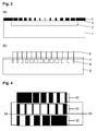
- a first embodiment of a laterally modulated correlation photo sensor device is disclosed in Figure 2(a). It makes use of a photosensitive element that accumulates and stores photo-generated charge carriers, and which is electrically contiguous.
- the disclosed embodiment uses a photodiode as a photosensitive element.
- a semiconductor substrate 1 of a first conduction type a shallow region 2 of the opposite conduction type with a thickness of 10 nm to 10 ⁇ m is fabricated, thus forming a photodiode.
- An electrically insulating layer 3, such as SiO 2 or Si 3 N 4 covers the semiconductor substrate.
- An optically opaque layer 4 such as metal, particularly Aluminum, covers the insulator 3. The layer has rectangular openings whose averaged width is proportional to the correlation function.
- the resulting laterally modulated mask 4 provides an averaged local light intensity on the photodiode 2,1 corresponding to the test function t(x).
- a second embodiment of a laterally modulated correlation photo sensor device is disclosed in Figure 2(b), and makes use of a multitude of individual photosensitive elements, whose averaged effective width is proportional to the corresponding amplitude of the correlation function.
- the individual photosensitive elements must be electrically connected, for example with a conducting line 8.
- this is achieved with a semiconductor substrate 5 of a first conduction type, into which several shallow regions 6 of the opposite conduction type with a thickness of 10 nm to 10 ⁇ m are fabricated, thus forming a plurality of photodiodes.
- the width of theses photodiodes is laterally modulated such that the average local width corresponds to the test function t(x).
- the device is covered with an insulation layer 7 protecting it electrically, chemically and mechanically from adverse outside influences. All photodiodes are electrically connected with a conduction line 8, which is either placed on the top of the device or at the side of it.
- the effective electrical capacitance is given by the sum of the individual capacitances of all components, and it is therefore linearly dependent on the electrically active surface. It is known that the noise that limits the performance of a photo sensor is proportional to the effective capacitance at the input of the first transistor, as described for example in P. Seitz, “Solid-State Image Sensing", in Computer Vision and Applications - A Guide for Students and Practitioners (B. Jähne and H. Haussecker, Eds.), pp. 111-152, Academic Press, San Diego, 2000 . This implies that the larger the photo sensor, the larger is its capacitance, and the higher is the charge noise that corrupts the signal, consisting of a certain number of photo charges.
- a MOS structure is used as the photosensitive element, and by making use of a lateral electrical field that separates the tasks of generating charge carriers generated by incident photons, and of accumulating these photo-generated charge carriers, as described for example in EP 1624490 A1 .
- the MOS structure of such an embodiment of a device according to the invention consists of a substrate 10 of a selected electrical conduction type, on top of which an isolation layer 13 is placed, capped with a high-resistivity electrode 14, which is biased to a positive potential in the case of a p-doped substrate 10, or biased to a negative potential in the case of an n-doped substrate 10.
- a p-doped substrate 10 is electrically connected to a p+ diffusion 11.
- a transparent insulator 13 is placed, with a thickness of 1 nm to 10 ⁇ m.
- This insulator 13 is covered with an electrically highly resistive transparent electrode 14, which has electrical connections 17 and 18 at opposite ends.
- a positive voltage difference between the two electrodes 18 and 17 creates a small current from contact 18 to contact 17, which in turn creates a linear potential drop at the surface of the semiconductor substrate 10, as illustrated in the lower part of Figure 3(a).
- Photo-generated charge carriers are rapidly swept to one side of the device, where they are accumulated and stored, either in an n+ diffusion 19, which is electrically connected through the contact 12, or, alternatively, under the gate of an MOS structure.
- the effective capacitance of the accumulation/storage structure 19 can therefore be very small, and, consequently, the correlation photo sensor device exhibits very small charge noise, being very sensitive as a result.
- the correlation functionality is realized by covering the device with an insulator 15, on top of which an opaque layer 16 is fabricated, which has laterally width-modulated rectangular openings as described above and acts as a mask.
- the height of the rectangular photosensitive elements is not prescribed, it is possible to create several tracks of photosensitive elements at the same time, arranged adjacent to each other in the direction perpendicular to the direction of the width modulation, as illustrated in Figure 4 for an embodiment with three tracks.
- Each of the tracks is capable of carrying out the correlation of the incident one-dimensional wave-field with a separate correlation test function, and all tracks carry out their correlation tasks simultaneously.
- the three tracks are electrically connected using the above-described method for creating lateral electrical fields, as shown in Figure 3. All electrical contacts to the transparent high-resistivity layer are electrically connected to the same electrical connections 33 and 34 at both sides of the devices.
- a positive voltage applied between the electrodes 34 and 33 leads to a lateral electrical field under the different tracks, sweeping the photo-generated electrons to the charge accumulation/storage diffusions that are individually read out for each correlation function track with separate electrical contacts 30, 31 and 32.
- Another possible embodiment combines the arrangements according to the previously described embodiments with the amplitude modulation of the photosensitive track according to the photo sensor devices described in CH 690971 A5 .
- This additional modulation h(x) can further enhance the effectively observed resolution of the test function t(x), and hence increases the applicability of the photo sensor devices to further high-resolution applications in optical linear and rotational encoders way beyond what has been possible with prior applications according to CH 690971 A5 and similar.
Landscapes
- Physics & Mathematics (AREA)
- General Physics & Mathematics (AREA)
- Solid State Image Pick-Up Elements (AREA)
- Light Receiving Elements (AREA)
Applications Claiming Priority (1)
| Application Number | Priority Date | Filing Date | Title |
|---|---|---|---|
| US82810206P | 2006-10-04 | 2006-10-04 |
Publications (1)
| Publication Number | Publication Date |
|---|---|
| EP1909075A2 true EP1909075A2 (de) | 2008-04-09 |
Family
ID=38924486
Family Applications (1)
| Application Number | Title | Priority Date | Filing Date |
|---|---|---|---|
| EP20070117600 Withdrawn EP1909075A2 (de) | 2006-10-04 | 2007-10-01 | Fotosensor mit räumlicher Korrelation |
Country Status (1)
| Country | Link |
|---|---|
| EP (1) | EP1909075A2 (de) |
-
2007
- 2007-10-01 EP EP20070117600 patent/EP1909075A2/de not_active Withdrawn
Similar Documents
| Publication | Publication Date | Title |
|---|---|---|
| EP1624490B1 (de) | Grossflächiger Pixel für die Verwendung in einem Bildsensor | |
| TW503573B (en) | Imager structure | |
| KR100451540B1 (ko) | 방사선 검출장치 | |
| US7462863B2 (en) | Thin film phototransistor, active matrix substrate using the phototransistor, and image scanning device using the substrate | |
| US20090121308A1 (en) | Image sensing device and method of | |
| EP1326278A2 (de) | Bildsensor mit leistungssteigernden Strukturen | |
| US20120242621A1 (en) | Image sensor and display device incorporating the same | |
| EP1583150A1 (de) | Bildsensor mit grossflächigen, hochgeschwindigen, hochempfindlichen Pixeln | |
| EP1477776B1 (de) | Fotoelektrische Kodiereinrichtung | |
| JP7650000B2 (ja) | フォトセンサ及びそれを用いた距離測定システム | |
| EP1624491A1 (de) | Festkörperbildsensor mit elektronischer Kontrolle der Apertur | |
| US4764682A (en) | Photosensitive pixel sized and shaped to optimize packing density and eliminate optical cross-talk | |
| WO1999018614A1 (en) | Prevention of photoelectric conversion layer contamination in an imaging device | |
| JP3996719B2 (ja) | 光電性チップ | |
| EP1909075A2 (de) | Fotosensor mit räumlicher Korrelation | |
| JP5271104B2 (ja) | リニアイメージセンサ | |
| KR102834561B1 (ko) | 광 검출 장치, 및 광 센서의 구동 방법 | |
| EP0631327A2 (de) | Photoempfindliche Niederkapazität Bauelemente für eine Bildsensoranordnung | |
| WO2010092929A1 (ja) | イメージセンサ | |
| JP4947404B2 (ja) | フォトセンサ及びその製造方法 | |
| JP4444715B2 (ja) | 光学式変位測定装置 | |
| de Lima Monteiro et al. | Integration of a Hartmann-Shack wavefront sensor | |
| KR100684581B1 (ko) | 포인팅 장치 | |
| Monteiro et al. | Integration of a Hartmann-Shack Wavefront Sensor | |
| EP1715528B1 (de) | Bildsensorphotodiodenanordnung |
Legal Events
| Date | Code | Title | Description |
|---|---|---|---|
| PUAI | Public reference made under article 153(3) epc to a published international application that has entered the european phase |
Free format text: ORIGINAL CODE: 0009012 |
|
| AK | Designated contracting states |
Kind code of ref document: A2 Designated state(s): AT BE BG CH CY CZ DE DK EE ES FI FR GB GR HU IE IS IT LI LT LU LV MC MT NL PL PT RO SE SI SK TR |
|
| AX | Request for extension of the european patent |
Extension state: AL BA HR MK RS |
|
| RAP1 | Party data changed (applicant data changed or rights of an application transferred) |
Owner name: CSEM CENTRE SUISSE D'ELECTRONIQUE ET DE MICROTECHN |
|
| STAA | Information on the status of an ep patent application or granted ep patent |
Free format text: STATUS: THE APPLICATION IS DEEMED TO BE WITHDRAWN |
|
| 18D | Application deemed to be withdrawn |
Effective date: 20150501 |