EP1906231A1 - Lumineszierende Anzeigevorrichtung - Google Patents
Lumineszierende Anzeigevorrichtung Download PDFInfo
- Publication number
- EP1906231A1 EP1906231A1 EP07021869A EP07021869A EP1906231A1 EP 1906231 A1 EP1906231 A1 EP 1906231A1 EP 07021869 A EP07021869 A EP 07021869A EP 07021869 A EP07021869 A EP 07021869A EP 1906231 A1 EP1906231 A1 EP 1906231A1
- Authority
- EP
- European Patent Office
- Prior art keywords
- optical
- luminescent material
- radiant energy
- display device
- luminescent
- Prior art date
- Legal status (The legal status is an assumption and is not a legal conclusion. Google has not performed a legal analysis and makes no representation as to the accuracy of the status listed.)
- Withdrawn
Links
Images


Classifications
-
- G—PHYSICS
- G02—OPTICS
- G02F—OPTICAL DEVICES OR ARRANGEMENTS FOR THE CONTROL OF LIGHT BY MODIFICATION OF THE OPTICAL PROPERTIES OF THE MEDIA OF THE ELEMENTS INVOLVED THEREIN; NON-LINEAR OPTICS; FREQUENCY-CHANGING OF LIGHT; OPTICAL LOGIC ELEMENTS; OPTICAL ANALOGUE/DIGITAL CONVERTERS
- G02F2/00—Demodulating light; Transferring the modulation of modulated light; Frequency-changing of light
- G02F2/02—Frequency-changing of light, e.g. by quantum counters
-
- G—PHYSICS
- G02—OPTICS
- G02F—OPTICAL DEVICES OR ARRANGEMENTS FOR THE CONTROL OF LIGHT BY MODIFICATION OF THE OPTICAL PROPERTIES OF THE MEDIA OF THE ELEMENTS INVOLVED THEREIN; NON-LINEAR OPTICS; FREQUENCY-CHANGING OF LIGHT; OPTICAL LOGIC ELEMENTS; OPTICAL ANALOGUE/DIGITAL CONVERTERS
- G02F1/00—Devices or arrangements for the control of the intensity, colour, phase, polarisation or direction of light arriving from an independent light source, e.g. switching, gating or modulating; Non-linear optics
- G02F1/01—Devices or arrangements for the control of the intensity, colour, phase, polarisation or direction of light arriving from an independent light source, e.g. switching, gating or modulating; Non-linear optics for the control of the intensity, phase, polarisation or colour
- G02F1/0126—Opto-optical modulation, i.e. control of one light beam by another light beam, not otherwise provided for in this subclass
-
- G—PHYSICS
- G02—OPTICS
- G02F—OPTICAL DEVICES OR ARRANGEMENTS FOR THE CONTROL OF LIGHT BY MODIFICATION OF THE OPTICAL PROPERTIES OF THE MEDIA OF THE ELEMENTS INVOLVED THEREIN; NON-LINEAR OPTICS; FREQUENCY-CHANGING OF LIGHT; OPTICAL LOGIC ELEMENTS; OPTICAL ANALOGUE/DIGITAL CONVERTERS
- G02F1/00—Devices or arrangements for the control of the intensity, colour, phase, polarisation or direction of light arriving from an independent light source, e.g. switching, gating or modulating; Non-linear optics
- G02F1/29—Devices or arrangements for the control of the intensity, colour, phase, polarisation or direction of light arriving from an independent light source, e.g. switching, gating or modulating; Non-linear optics for the control of the position or the direction of light beams, i.e. deflection
- G02F1/293—Devices or arrangements for the control of the intensity, colour, phase, polarisation or direction of light arriving from an independent light source, e.g. switching, gating or modulating; Non-linear optics for the control of the position or the direction of light beams, i.e. deflection by another light beam, i.e. opto-optical deflection
Definitions
- the present invention relates generally to the use of a luminescent compound radiated by energy propagated from the side of a waveguide such as an optical fiber, and in particular to a luminescence matrix made from coincidentally-excited phosphors, an optical display device and an optical switch using the same, and a control method for the luminescence matrix.
- Displays are often of a cathode ray tube (CRT) or liquid crystal display construction.
- CRT cathode ray tube
- An example of a liquid crystal display panel is described by Funada, et al. in U.S. Pat. No. 4,231,640 .
- the conventional construction of displays has typically involved high-voltage components and the emission of electromagnetic radiation and electromagnetic interference (EMI) from the display panel. Size and weight characteristics of conventional displays often make portability difficult or inconvenient. Also, durability of the display can be troublesome, due to the high number of electronic parts, or alignment required of various components.
- EMI electromagnetic radiation and electromagnetic interference
- each optical fiber is either “on” or “off,” causing an entire row of notches to emit the visible light transmitted through the fiber simultaneously.
- Each row of notches is also limited to the same color of visible light transmitted through the common optical fiber. None of these technologies combine luminescent materials with side-emitting optical fibers.
- U.S. Patent No. 5,432,876 discloses an optical fiber having a light emitting region to propagate light from an optical fiber in a preselected direction.
- One embodiment of the U.S. Patent No. 5,432,876 involves mounting of optical fibers to a panel so as to form a substantially parallel array.
- a liquid crystal shutter array (LCS) is formed in front of the substantially parallel array so as to block unwanted notch emissions from view.
- the U.S. Patent 876 only teaches the redirection of light from the notch of an optical fiber and not the illumination of a luminescent material.
- U.S. Patent No. 5,659,643 discloses a notched fiber array illumination device.
- the U.S. Patent '643 is similarly limited to only teaching the redirection of light from an optical fiber, but does teach a Fresnel lens or other beam turning device can be used to further redirect light emitted from the notch of an optical fiber.
- a method for producing visible light from a luminescent material is to transmit radiation through a side-emitting optical waveguide to radiate a luminescent material and produce visible light. This allows for an optical luminescent display device to be constructed without electronic components.
- the side-emitting optical waveguide contains a notch, wherein the notch is configured so as to direct radiation energy within the fiber toward a luminescent material.
- an optical luminescent display device includes a luminescent material; and side emitting optical waveguide means adapted for supplying radiant energy to the luminescent material.
- an optical luminescent display device adapted for use with a radiant energy source, includes an optical waveguide; a luminescent material; and a notch formed in the optical waveguide adapted to direct a first type of radiant energy within the optical waveguide toward the luminescent material.
- a luminescent matrix of optical waveguides capable of coincidentally-radiating pixels of luminescent material. This allows for matrix-addressing of individual pixels within a display panel.
- an optical luminescent display device includes: a luminescent material; a first energy source which generates a first radiant energy for continuously illuminating said luminescent material ; and a second energy source which generates a second radiant energy for selectively illuminating said luminescent material to thereby control emission of visible light.
- an optical luminescent display device includes: a luminescent material; a first energy source which generates a first radiant energy for illuminating said luminescent material; and a second energy source which generates a second radiant energy for illuminating said luminescent material to thereby control emission of visible light, wherein said luminescent material converts said first radiant energy to visible light and ceases to emit said visible light when illuminated by said second radiant energy.
- an optical luminescent display device includes: a luminescent material; a first energy source which generates a first radiant energy for continuously illuminating said luminescent material; a second energy source which generates a second radiant energy for selectively illuminating said luminescent material to thereby control emission of visible light; a plurality of pixels containing said luminescent material; and a substrate shaped to evenly distribute said first radiant energy to said plurality of pixels.
- a control method therefor includes the steps of: selecting a plurality of dots from the plurality of dots; selecting at least one dot from the selected plurality of dots; illuminating the selected plurality of dots with a first radiant energy and said at least one dot with a second radiant energy to thereby control emission of visible light at said at least one dot.
- the first radiant energy causes the selected plurality of dots to be sensitized and the second radiant energy causes said at least one dot thereof to emit visible light.
- one of the first and second radiant energies causes a selected dot to emit visible light and both thereof cause the selected dot not to emit visible light.
- a second embodiment of the invention is an optical switch.
- the optical switch involves radiation provided from within a side emitting optical fiber and, upon activation of the optical switch, a second radiation provided by a laser diode or infrared LED.
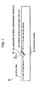
- the optical luminescent display device 30 is comprised of an optical waveguide 32 that includes a notch 34.
- the optical waveguide 32 is made of an optically transmissive substance, such as plastic or glass.
- an optical fiber can be used as the optical waveguide 32.
- Virtually any diameter of optical waveguide 32 can be used. If a glass optical fiber is used, a diameter of approximately 125 microns to 1 mm is typical.
- the notch 34 contains a luminescent material 36, such as a phosphor or fluorescent material.
- the notch 34 may be left open or filled in with a filling material 38.
- the filling material 38 could be a typical optical filler substance known in the art, or it could be a luminescent material. Filling in the notch results in a stronger structure and enhanced optical properties.
- the depth of the notch can vary. If multiple notches are provided on a single optical fiber and a light, e.g. radiation, source is provided from only one side, the depth of each notch 34 can be increased as the notches are located further from the light source. This allows for equal illumination of each notch, even though some notches are further from the light source.
- the notch 34 is shown in the shape of a right triangle, but can be formed at a variety of angles. Also, the notch 34 can be a narrow slit, just wide enough for the luminescent material 36 to be deposited. Although only one notch is shown, a plurality of notches may be formed in the optical fiber 32. The notches do not necessarily need to be oriented in the same direction; they may be formed to face multiple directions.
- the phosphor thickness is approximately typically 50 to 100 microns.
- the luminescent material 36 may be mounted as shown in Figure 1, or on the outside edge of a notch 34 containing filling material 38, or may be a coating large enough to cover both the outside edge of the optical fiber 32 and fill in the notch 34, or transversally-opposite side of the optical fiber 32 from the notch 34, similar to the location of the reflective coating 42 shown in Figure 1.
- the luminescent material 36 can also be formed as a sheet, providing for easier application to multiple optical fibers.
- a dichroic filter 40 is located between the luminescent material 36 and the optical fiber 32.
- the dichroic filter 40 allows infrared (IR) light to pass, but reflects visible light.
- a reflective coating 42 may be mounted on the optical fiber 32 transversally opposite from the notch 34. The reflective coating 42 reflects all types of radiation. Both IR and visible light are reflected by reflective coating 42 as shown in Figure 1.
- the operation of the optical luminescent display device 30 is as follows. Radiation is provided through the optical fiber 32 so that it communicates with the luminescent material 36, causing the luminescent material 36 to emit visible light. Visible light is then projected from the luminescent material 36. If present, the dichroic filter 40 and the reflective coating 42 each serve to enhance the visible light emitting from the luminescent material 36 so as to brighten the display.
- the dichroic filter 40 reflects visible light and therefore reflects the visible light emitted by the luminescent material 36 outward and helps to keep the visible light out of the optical fiber 32.
- the reflective coating 42 reflects radiation passing through the optical fiber 32, such as IR light, ultraviolet (UV) light, or visible light that may be deflected downward by the notch 34.
- the reflective coating 42 reflects any radiation, such as IR light back in the direction of the notch 34 to enhance the amount of radiation reaching the luminescent material 36. Visible light emitted by the luminescent material is similarly reflected so as to enhance the amount of visible light emitted in the direction of the viewer.
- Phosphorescence is the emission of light from certain inorganic materials following excitation by photons, electrons, or high-energy radiation. Absorption of the incident radiation occurs because valence-band electrons in the material are excited to higher-energy states. In normal materials and in fluorescent substances the excited electron returns quickly to the ground state, and emission of light decays very soon after cessation of the incident, i.e. exciting, radiation. In phosphorescent materials, in contrast, the decay of the excited state is prolonged, often because the excited electrons are trapped at acceptor states just below the conduction band.
- the radiation provided through the optical fiber 32 may be IR light, UV light, visible light, or any radiation or energy that serves to cause the luminescent material 36 to emit visible light.
- the luminescent material 36 is double illumination, i.e. co-incident, luminescent material and does not emit visible light until two wavelengths of light communicate with it.
- UV light 44 is radiated from one direction and IR light 46 is radiated from another direction.
- the UV light 44 is typically of a wavelength approximately of 200 to 380 nm.
- the IR light 46 is typically of a wavelength approximately of 700 to 1380 nm.
- the direction from which the light is radiated may be reversed or radiated from the same side.
- Other luminescent material 36 which is single illumination luminescent material, only requires one wavelength of light to communicate with it to cause it to emit visible light.
- Eu++ has a 4f ground state just above the valence band of the lattice, and a 5d excited state just below the conduction band. Blue or UV light, depending on the composition of the phosphor, excites the Eu++ ion to the 4d state. Sm++ creates traps just below the conduction band in these materials. By a charge-transfer mechanism, the excited Eu++ electron is quickly transferred to a Sm+++ trap. The trap state is more than 1 eV below the conduction band and quite stable. Formally, the Eu++ becomes Eu+++ (Eu++ with a bound hole) and the Sm+++ becomes Sm++ via a charge-transfer reaction.
- the phosphor In this state the phosphor is primed. Irradiating the phosphor with IR light of 980 nm, although 1.1 ⁇ m or so is best, kicks electrons out of the Sm traps and allows them to fall back into the Eu 5d excited state.
- the Eu 5d to 4f transition back to the ground state produces visible light emission peaking at about 640 nm; the difference between the wavelengths of the excitation and emission maxima is due to Stokes shift.
- the maximum amount of light which can be liberated during photostimulation is limited only by saturation of the Sm co-activator sites.
- the process of excitation proceeds by a two step mechanism: incident light of one wavelength, typically blue or UV, excites electrons directly to the conduction band and these electrons quickly migrate to acceptor states or 'traps' with energy somewhat below the conduction band. These states have a relatively long lifetime.
- the phosphor is said to be 'sensitized' when a significant fraction of these acceptor states are occupied. Subsequent irradiation of such a sensitized phosphor with light of a second wavelength, often red or IR wavelength, can induce transitions from the acceptor states to higher-energy states which decay by normal phosphorescence.
- the two most common storage phosphors have broad band emission at 520 nm and 650 nm and are intended for monochromatic application.
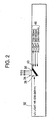
- Figures 2-4 illustrate the ability to change the color of the visible light emitted by a double illumination phosphor by adjusting the amount of radiation of IR light or UV light within various frequency bands. For example, as shown in Figure 2, with sensitizing UV radiation between 200 and 380 nm and using a EuSm phosphor, blue light is emitted if IR light of approximately between 700 and 780 nm is supplied. Green light is emitted if IR light of approximately between 830 and 900 nm is supplied. Red light is emitted if IR light of approximately between 980 and 1180 nm is supplied.
- Figure 4 illustrates that with sensitizing IR radiation between 700 and 1380 nm, using a EuSm phosphor, blue light is emitted if UV light of approximately 255 nm is supplied. Green light is emitted if UV light of approximately 302 nm is supplied. Red light is emitted if UV light of approximately 365 nm is supplied.
- Figure 5 illustrates another variation of the optical luminescent display device 30.
- This variation is intended to provide radiation 50 in the optical fiber 32 from one direction.
- the radiation 50 can be any type of radiation that will cause the single-illumination luminescent material 36 to emit the desired radiation wavelength.
- the luminescent material 36 is a phosphor
- UV light of 200-380 nm or IR light of 700-1380 nm can be used to cause the luminescent material 36 to emit visible light.
- YVO 4 :Eu or 3.5MgO ⁇ 0.5MgF 2 ⁇ GeO 2 :Mn phosphors can be used.
- Zh ⁇ Ge ⁇ O ⁇ Mn phosphor can be used.
- (SrCaBa) 5 (PO 4 ) 3 Cl:Eu phosphor can be used.
- the above listed phosphors are activated by UV light between 200-380 nm, ideally 365 nm, and are commercially available from Nichia Chemical Industries, Ltd., part numbers NP-312, NP-320, NP-202, NP-105, respectively.
- the notch 34 is provided with a mirror coating 48 to enhance the amount of radiation provided to the luminescent material 36 and reduce the amount of visible light emitted by the luminescent material 36 entering the optical fiber 32.
- An optical switch device 60 is shown in Figure 6.
- An optical luminescent display device 30 is provided with a luminescent material 36 and one or more optical pickups 62.
- a dichroic filter 40 is optional.
- the luminescent material 36 is a double illumination luminescent material, requiring two types of radiation to emit visible light.
- the optical switch device 60 is activated when both types of radiation are provided within the optical fiber 32 to cause the luminescent material 36 to emit visible light. For example, when both UV light 44 and IR light 46 are provided, a luminescent material 36, such as a phosphor, will emit visible light.
- the optical pick up 62 which may be accompanied by another optical pick up 62, pick up the visible light to provide the switch output to the desired location.
- UV light 44 is radiated within the optical fiber 32 from either direction.
- An optical switch 90 is formed from a laser diode 92 arranged to provide IR light to a luminescent material 36 located in or near notch 34 of optical fiber 32. UV light 44 is provided within the optical fiber 32.
- the laser diode 92 is activated, thereby providing IR light to the luminescent material 36.
- the luminescent material 36 is a double illumination luminescent material, requiring two types of radiation to emit visible light. UV light 44 is already provided in the optical fiber 32. Therefore, when the laser diode 92 provides IR light, the luminescent material 36 emits visible light.
- each optical switch 90 is formed from a luminescent material 36 activated by a different frequency of IR light than that of nearby optical switches 90. Therefore, a corresponding frequency laser diode 92 is used to activate the luminescent material 36 in each optical switch 90, allowing closer spacing of the optical switches 90.
- an IR LED can be used in place of the laser diode 92.
- both embodiments of the optical switch can be operated using radiation types other than discussed above, such as visible light or any energy capable of causing the luminescent material 36 to emit the desired radiation.
- a luminescent material 36 to provide a non-visible output, such as IR, for example, may also be used.
- IR and UV radiation can be reversed in the descriptions above.
- FIG. 17 and 23-26 illustrate examples of such a matrix configuration.
- Figures 8-14 provide a variety of examples of the structure that can be used for each pixel of the optical display panel.
- Figures 23-25 are perspective views of examples of the structure of an optical display panel.
- Figure 26 illustrates an optical display panel with detailed structural elements omitted for clarity.
- a double illumination luminescent material can be used as the basis for a coincidentally-addressed optical display panel.
- Side-emitting optical fibers (T. Wang et al., U.S. Patent No. #5,673,344) are ideally-suited to provide coincident illumination of the luminescent pixel elements in a display of this type, as seen in Figures 8-14 and 24.
- U.S. Patent No. #5,673,344 is incorporated herein by reference in its entirety.
- One optical fiber in these figures delivers 'sensitizing' (typically blue or UV wavelength) radiation to one row of phosphor pixels at a time, while another fiber delivers secondary exciting radiation (typically red or IR) to each column of phosphor pixels.
- Pixel elements which receive either (i) 'sensitizing' radiation only or (ii) 'secondary' radiation only do not emit light. With only a single horizontal fiber and a single vertical fiber active, only the pixel at the intersection of these fibers will radiate light. By the well-known method of sequential activation or time-multiplexing of the horizontal and vertical fibers, an image may be displayed.
- two optical fibers 32 are used to provide radiation to a luminescent material 36.
- UV light 44 is provided by one optical fiber 32 to sensitize the luminescent material 36, located between the optical fibers 32.
- IR light 46 is provided by the other optical fiber 32.
- a mirror 48 may be used to increase the amount of UV light 44 that reaches the luminescent material 36 and reduce the amount of visible light emitted by the luminescent material entering the optical fiber 32 having the mirror 48.
- a mirror 48 is not used on the other optical fiber 32 because the visible light shines through this optical fiber 32 for viewing. The direction of viewing of the device in Figure 8 is shown by arrow A.
- UV light 46 and IR light 44 are described above, any radiation can be used that will cause the luminescent material 36 to emit the desired wavelength of radiation, such as visible light.
- Figure 9 shows a structure similar to that shown in Figure 8, except that, by way of example, a different position of the luminescent material 36 is shown.
- the notch 34 containing luminescent material 36 contains a filling material 38 so as to hold the luminescent material 36 in place.
- Other possibilities are available for the location of luminescent material 36.
- luminescent material 36 may be located in one of the notches 34 at an angle or parallel to the axis of the optical fibers 32.
- Figure 10 shows a structure similar to that shown in Figure 8, except that, by way of example, a different notch 152 configuration is shown. A variety of combinations of notch shape and location are possible.
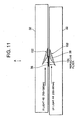
- Figure 11 adds reflective filter 154.
- the reflective filter 154 can be configured to allow UV light 44 to pass, but reflect visible light. This would enhance the visible light emitted from the luminescent material 36 in the direction of the viewer. The direction of viewing is shown by arrow A.
- Notch 152 may be open or filled with filling material 38.
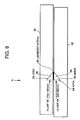
- Figure 12 involves a notch 182 containing a reflection pyramid 190.
- the reflection pyramid 190 is ideally formed with its peak set in from the edge of the optical fiber 32, to distribute radiation to the luminescent material 36, as shown by the exemplary small arrows, regardless of the direction from which the radiation is provided.
- the reflection pyramid 190 can be inserted into the notch 182, or the notch 182 can be formed with an inner edge forming a reflection pyramid 190.
- the area 192 within the notch 182 may be left open or, preferably, filled with a filling material.
- the optional dichroic filter 186 increases the amount of IR light 46 and discharge UV light 188 directed toward the luminescent material 36.
- Discharge UV light 188 is provided to adjust the charge within the luminescent material 36.
- the discharge UV light 188 at a wavelength of between 200 and 380 nm, increases the charge of the luminescent material 36 so as to prevent or discontinue the emission of visible light from the luminescent material 36. This, in essence, restarts the sensitizing/excitation process for the luminescent material 36.
- Another process of applying UV light 44 can be followed by IR light 46 to result in the emission of visible light by the luminescent material 36. See Figures 21 and 22 as examples of timing charts that could be used in the application of discharge UV light 188, IR light 46, and UV light 44.
- the timing of Figure 22 is preferred over that of Figure 21, because the UV light has time to sensitize the luminescent material prior to the application of the exciting IR light.
- a discharge UV light 188 may not be necessary. In such a case, the emission of visible light would cease upon either UV light 44 or IR light 46 not being provided.
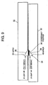
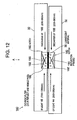
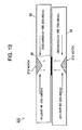
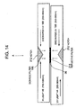
- Figure 13 shows notches 212 formed on the outer sides of the optical fibers 32.
- Figure 14 adds a dichroic filter 186.
- the dichroic filter 186 reflects UV light and IR light, but allows visible light to pass.
- the dichroic filter 186 increases the amount of IR light 46 and discharge UV light 188 directed toward the luminescent material 36. However, visible light is allowed to pass to the viewer, who is viewing in the direction of the arrow A.
- Figure 14 shows the preferred location and orientation of the notches 212 with respect to the luminescent material 36 for the optical display panel of the invention.
- Figures 8-14 show the fibers as parallel, the fibers can be perpendicular as shown in Figures 17, and 23-26, or at any angle.
- Parallel orientation is the least desirable orientation, as a row and column configuration can not be established with all the optical fibers oriented in the same direction, thereby frustrating individual pixel addressing.
- Multi-color luminescent materials can be used such that the color of each pixel of luminescent material is adjusted by providing the proper wavelength of sensitizing and/or exciting radiation.
- single-color luminescent materials can be used.
- Figures 15 and 16 show examples of single-color pixel configurations.
- Figure 15 illustrates a standard pixel layout 300 with red pixels 302, green pixels 304 and blue pixels 306 arranged in row or column order.
- the pitch will be 1.0 mm and the pixel width 95 mm, but these can be adjusted for various optical fiber diameters.
- the pixel color groups should be arranged diagonally, as shown in Figure 16.
- Red pixels 332, green pixels 334 and blue pixels 336 are shown in a preferred pixel layout 330.
- "R" "G” and “B” are shown in Figures 15 and 16 for illustrative purposes only.
- An optional black mask 338 is shown formed between each pixel. Use of the black mask 338 is preferable to enhance the clarity of the image displayed.
- a phosphor, BaFBr:Eu 2+ can be used for a red pixel that will illuminate upon exposure to both UV and IR light.
- the phosphors SrS:Ce:Sm or SrS:Eu:Sm can be used for a green pixel that will illuminate upon exposure to both UV and IR light.
- a Ba 3 (PO 4 ) 2 :Eu 2+ , La 3+ can be used for a blue pixel that will illuminate upon exposure to both UV and IR light.
- a perpendicular matrix 360 is shown in Figure 17.
- a pixel 370 a section or piece of luminescent material analogous to luminescent material 36, is addressed by radiation provided to the optical fibers 372 and 374.
- the pixel 370 analogous to luminescent material 36, is provided with UV light, from a UV source 368, IR light, from an IR light source 366, and UV discharge light, from a UV discharge source 364.
- Each of these light or discharge sources is directed via an addressing means 362 that selects one fiber per axis.
- the proper optical fiber 372 is selected from among the rows or the proper optical fiber 374 from among the columns.
- the sources can be arranged to provide radiation from the same end of the fiber.
- a UV discharge source 364 can be supplied from the same fiber end as the IR source 366. It is also possible to use one source per axis and adjust the wavelength of the output to the type of light required.
- a phosphor plate 398 shown in Figure 18, can be used.
- the phosphor plate 398 can be formed using a substrate, typically glass, although plastic is also suitable. Powdered phosphor is deposited upon the substrate. The powder can be deposited using processes such as printing, coating or sputtering.
- the substrate can be opaque, requiring radiation to be provided to the phosphor from the same side of the substrate as the phosphor. Alternatively, a transparent or translucent substrate may be used to allow radiation to be provided from both sides of the substrate.
- the preferred substrate for the optical display panel, shown in Figure 18, is transparent.
- a second type of phosphor plate 398 involves a phosphor film, available commercially, wherein the phosphor is mounted to a film.
- Figure 18 illustrates another embodiment of the optical display panel 390 from a side view.
- the optical display panel 390 is viewed in the direction of arrow A.
- the optical fiber 392 provides IR light and the optical fiber 394 provides UV light to a section of a phosphor plate 398 disposed between the optical fibers 392 and 394. This section of the phosphor plate 398 functions as a pixel 400 of the optical display panel.
- a discharge lamp 396 is provided at the rear of the display to provide discharge radiation from outside the optical fibers.
- the optical fiber 392 providing IR light and the optical fiber 394 providin UV light do not need to also provide discharge radiation, as it is provided by discharge lamp 396.
- the discharge radiation passes transversally through the optical fiber 394 to the phosphor plate 398.
- the discharge lamp 396 can illumine the phosphor plate 398 by way of a side-emitting optical fiber.
- the phosphor plate 398 can use a standard pixel layout 300, as shown in Figure 15, or a preferred pixel layout 330 of Figure 16. Alternatively, the phosphor plate 398 can be formed of multi-color luminescent material.
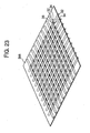
- Figures 23-26 provide perspective views of an example of an optical display panel.
- Figures 23 and 26 show an overall configuration of the optical display panel.
- Figures 23-25 illustrate a phosphor plate 398 mounted between optical fibers 32 arranged to have notches 34 located at the intersections of the optical fibers 32.
- a luminescent material 36 is mounted between the notches 34.
- the spacing of the optical fibers 32 oriented in the same direction can be increased or decreased.
- the luminescent material 36 is illustrated as individual pieces, one for each optical fiber 32 intersection, it is also possible to provide luminescent material 36 large enough to be mounted between multiple optical fiber 32 intersections, even covering the entire phosphor plate 398. In such a case, masking, such as black mask 338, discussed above in relation to Figures 15 and 16, is preferred.
- Figures 23-25 are progressive magnifications of the same example of an optical display panel.
- Figure 19 illustrates a radiation direction assembly 420. Radiation is provided by the laser array 422.
- the laser array 422 could produce UV light or IR light, or could be substituted with another radiation producing device. Ideally, the laser array 422 has an output of 30 to 40 W, but may also be of greater or lesser power.
- the lens array 424 focuses the radiation emitted from the laser array 422.
- the optical beam switch 426 directs the radiation to the proper optical fiber within the optical fiber bundle 430.
- Discharge radiation capable of illuminating all the optical fibers within the optical fiber bundle 430 simultaneously, is provided by a discharge light source 434.
- the discharge radiation is provided through a lens 432 into a beam splitter 428.
- the beam splitter is arranged to provide radiation to multiple optical fibers within the optical fiber bundle 430.
- a radiation direction assembly 450 can be used.
- Figures 20A and 20C illustrate this embodiment.
- a linear laser array 452 is used to provide a plurality of radiation sources.
- each of the emitters within the laser array 452 has an output of 30 to 40 W, but may also be of greater or lesser power.
- a lens array 454 and an optical beam switch 456 are also provided to focus and direct the radiation, respectively.
- the optical fiber bundle 458 can best be arranged, as shown by way of example in Figure 20B, such that the optical fibers that make up the columns of the optical display panel and optical fibers that make up the rows of the optical display panel are provided in one bundle. This allows the optical display panel to be operated from a single optical fiber bundle 458 and a single radiation direction assembly 450, if desired.
- a radiation direction assembly 450 can be provided for each axis of the optical display panel.
- optical display panels can be used in close proximity to each other, each displaying only a portion of the entire desired image.
- Such a configuration allows for lower powered radiation sources and the use of luminescent materials with slower response times, e. g. requiring longer application times for sensitization, excitation, or discharge radiation.
- Single illumination luminescent material e.g., requiring only one type of radiation to cause it to emit visible light, may also be used as the basis for an optical display panel.
- photostimulable phosphors typically known as 'ordinary' phosphors
- electrons are excited by blue or UV light, electron bombardment in a CRT, or absorption of X-ray or other radiation and return slowly to the ground state, producing a sustained but slowly-decaying 'phosphorescence' after the exciting source is turned off.
- the emission of light decays very quickly after the exciting source is turned off.
- the phosphor remains in an activated, e.g. sensitized, state, and shining long-wavelength light on the phosphor while it is in the activated state will cause the phosphor to emit visible light. In the dark, the activated state of the phosphor may persist for quite a long time - days or even weeks.
- the host lattice is a wide-bandgap II-VI material, typically in alkaline-earth sulfide (MgS, CaS, or SrS).
- the 'activator' species is typically europium (as Eu++) and the 'co-activator' species is typically samarium (as Sm+++), both present at about 100 ppm concentration.
- These are added as chloride salts, and some of the chloride ion enters the lattice. Cl substituting for S-- is believed to compensate the charge excess of Sm+++ substituting for M++ metal ion.
- the compositions are designated as host:(activators), e.g., SrS:(Sm, Eu).
- the generic phosphors include alkaline earth chalcogenides.
- Typical phosphors of this type include magnesium, calcium, strontium and barium sulfides. They are activated and sensitized with co-dopants which can trap electrons at shallow levels below the conduction band with subsequent infrared stimulation inducing radiative recombination processes, i.e., emission of light.
- co-dopants which can trap electrons at shallow levels below the conduction band with subsequent infrared stimulation inducing radiative recombination processes, i.e., emission of light.
- these storage phosphor materials have not found application in display applications. However, singly-doped materials have been used in electroluminescent display applications.
- Yet another embodiment of the invention overcomes these possible drawbacks by providing the following solutions: a) a "storage phosphor" which cannot be discharged, and b) a phosphor which converts UV light directly into visible light, but this conversion can be "switched off” with a coincidental IR light source.
- a storage phosphor can be viewed as a light amplifier.
- a high power UV light source provides the energy while a low-power IR beam controls the emission of visible light.
- the basic principle is shown in Figure 27.
- a screen 271 is coated with a grid of phosphor dots 272.
- a constant UV light source 273 keeps all dots charged.
- a specific dot 272a will emit visible light only when it is also illuminated by a beam of IR light 274 from an IR source 275.
- the inventors have obtained some samples of phosphor (ZnS:Sm) which directly converts UV light to visible light. In addition, this conversion can be suppressed with incidental IR light.
- the basic principle is shown in Figure 29.
- a screen 291 is coated with a grid of phosphor dots 292. Any phosphor dot which is illuminated only by the constant UV light source 294 will convert the UV light immediately and directly into visible light. However, if a dot 293 is also illuminated by an IR light source 295 the conversion to visible light will not take place and that particular dot will stay dark.
- a 2D grid 301 of side-emitting optical fibers 302 is used to distribute "blocking" IR light 303.
- a pixel 304 would emit visible light only if both the vertical fiber as well as the horizontal fiber associated with the pixel are "dark". If any one of these two fibers is carrying IR light, the pixel will stay dark.
- Figure 31 shows a possible assembly of a display using this method.
- a glass substrate 311 is shaped to evenly distribute the light from a UV source 312 to all phosphor pixels 313.
- An arrangement of vertical side emitting fibers 314, and horizontal side emitting fibers 315 provide the means to individually control any pixel.
- the IR source for each fiber may be provided by an individual IR laser diode 316 which in turn is controlled by some control logic 317 which coordinates the state of all IR sources to create a desired display pattern.
- FIG. 32 An alternative method to distribute the UV source is shown in Figure 32.
- the same fiber 321 (constructed, for example, to have notches 321a) which carries the control IR light 322 can also distribute the charging UV light 323.
- the display panel of the present invention is entirely optical and can be separate from the light sources, such as laser, LED or lamp, providing excitation.
- the display panel may connect to the electro-optical module via a flexible fiber optics cable. Because it is all-optical, a display panel of this type is expected to be especially rugged and will be able to operate in certain environments where electronic devices cannot be used. Also, the display panel will not have electronics part built in, such as TFT transistor, pixel drivers, electrode and line or column electrical wire. There is no high-voltage, no electromagnetic radiation, no EMI from the display panel. Due to the simple construction of a display panel of this type, the cost of manufacture is expected to be significantly lower than that of competitive display technologies.
Applications Claiming Priority (4)
| Application Number | Priority Date | Filing Date | Title |
|---|---|---|---|
| US9876998P | 1998-09-01 | 1998-09-01 | |
| US09/246,145 US6307987B1 (en) | 1998-09-01 | 1999-02-08 | Optical luminescent display device |
| US09/359,037 US6760515B1 (en) | 1998-09-01 | 1999-07-23 | All optical display with storage and IR-quenchable phosphors |
| EP99117223A EP0990944B1 (de) | 1998-09-01 | 1999-09-01 | Lumineszente Anzeigevorrichtung |
Related Parent Applications (1)
| Application Number | Title | Priority Date | Filing Date |
|---|---|---|---|
| EP99117223A Division EP0990944B1 (de) | 1998-09-01 | 1999-09-01 | Lumineszente Anzeigevorrichtung |
Publications (1)
| Publication Number | Publication Date |
|---|---|
| EP1906231A1 true EP1906231A1 (de) | 2008-04-02 |
Family
ID=38996476
Family Applications (3)
| Application Number | Title | Priority Date | Filing Date |
|---|---|---|---|
| EP07021867A Withdrawn EP1898259A1 (de) | 1998-09-01 | 1999-09-01 | Optische lumineszierende Anzeigevorrichtung |
| EP07021869A Withdrawn EP1906231A1 (de) | 1998-09-01 | 1999-09-01 | Lumineszierende Anzeigevorrichtung |
| EP07021868A Withdrawn EP1895358A3 (de) | 1998-09-01 | 1999-09-01 | Optische Leuchtanzeigenvorrichtung |
Family Applications Before (1)
| Application Number | Title | Priority Date | Filing Date |
|---|---|---|---|
| EP07021867A Withdrawn EP1898259A1 (de) | 1998-09-01 | 1999-09-01 | Optische lumineszierende Anzeigevorrichtung |
Family Applications After (1)
| Application Number | Title | Priority Date | Filing Date |
|---|---|---|---|
| EP07021868A Withdrawn EP1895358A3 (de) | 1998-09-01 | 1999-09-01 | Optische Leuchtanzeigenvorrichtung |
Country Status (1)
| Country | Link |
|---|---|
| EP (3) | EP1898259A1 (de) |
Citations (7)
| Publication number | Priority date | Publication date | Assignee | Title |
|---|---|---|---|---|
| US3927323A (en) * | 1973-09-20 | 1975-12-16 | Us Navy | Video phosphor motion perception display |
| US4231640A (en) | 1977-07-07 | 1980-11-04 | Sharp Kabushiki Kaisha | Matrix type liquid crystal display panel |
| WO1990012387A1 (en) * | 1989-04-07 | 1990-10-18 | Aubusson Russell C | Laser-written moving image display apparatus |
| JPH04323686A (ja) * | 1991-04-23 | 1992-11-12 | Clarion Co Ltd | ディスプレイ装置 |
| US5432876A (en) | 1992-10-19 | 1995-07-11 | Minnesota Mining And Manufacturing Company | Illumination devices and optical fibres for use therein |
| US5659643A (en) | 1995-01-23 | 1997-08-19 | Minnesota Mining And Manufacturing Company | Notched fiber array illumination device |
| US5673344A (en) * | 1996-06-20 | 1997-09-30 | Nec Research Institute, Inc. | Bi-directional light port for injecting light into and tapping light from a side of an optical fiber |
Family Cites Families (3)
| Publication number | Priority date | Publication date | Assignee | Title |
|---|---|---|---|---|
| US4578709A (en) | 1984-08-03 | 1986-03-25 | Allen Jensen | Flat optical TV screen |
| WO1990002349A1 (en) * | 1988-08-31 | 1990-03-08 | Raynet Corporation | Method of deforming a polymer optical fiber to form taps |
| US5541012A (en) * | 1992-05-08 | 1996-07-30 | Nippon Telegraph And Telephone Corporation | Infrared-to-visible up-conversion material |
-
1999
- 1999-09-01 EP EP07021867A patent/EP1898259A1/de not_active Withdrawn
- 1999-09-01 EP EP07021869A patent/EP1906231A1/de not_active Withdrawn
- 1999-09-01 EP EP07021868A patent/EP1895358A3/de not_active Withdrawn
Patent Citations (8)
| Publication number | Priority date | Publication date | Assignee | Title |
|---|---|---|---|---|
| US3927323A (en) * | 1973-09-20 | 1975-12-16 | Us Navy | Video phosphor motion perception display |
| US4231640A (en) | 1977-07-07 | 1980-11-04 | Sharp Kabushiki Kaisha | Matrix type liquid crystal display panel |
| WO1990012387A1 (en) * | 1989-04-07 | 1990-10-18 | Aubusson Russell C | Laser-written moving image display apparatus |
| JPH04323686A (ja) * | 1991-04-23 | 1992-11-12 | Clarion Co Ltd | ディスプレイ装置 |
| US5432876A (en) | 1992-10-19 | 1995-07-11 | Minnesota Mining And Manufacturing Company | Illumination devices and optical fibres for use therein |
| US5432876C1 (en) | 1992-10-19 | 2002-05-21 | Minnesota Mining & Mfg | Illumination devices and optical fibres for use therein |
| US5659643A (en) | 1995-01-23 | 1997-08-19 | Minnesota Mining And Manufacturing Company | Notched fiber array illumination device |
| US5673344A (en) * | 1996-06-20 | 1997-09-30 | Nec Research Institute, Inc. | Bi-directional light port for injecting light into and tapping light from a side of an optical fiber |
Non-Patent Citations (3)
| Title |
|---|
| SCHEPS R: "Pulsed laser stimulation and excitation in ZnS:Pb,Mn phosphor", JOURNAL OF LUMINESCENCE NETHERLANDS, vol. 29, no. 4, July 1984 (1984-07-01), pages 413 - 432, XP002470053, ISSN: 0022-2313 * |
| SWIATEK K ET AL: "Recombination processes in ZnS:Sm", PHYSICAL REVIEW B (CONDENSED MATTER) USA, vol. 43, no. 12, 15 April 1991 (1991-04-15), pages 9955 - 9958, XP002470054, ISSN: 0163-1829 * |
| TABEI M ET AL: "Mechanism of infrared stimulation and quenching in ZnS:Cu, Al phosphors", JOURNAL OF LUMINESCENCE NETHERLANDS, vol. 15, no. 2, June 1977 (1977-06-01), pages 201 - 215, XP002470052, ISSN: 0022-2313 * |
Also Published As
| Publication number | Publication date |
|---|---|
| EP1898259A1 (de) | 2008-03-12 |
| EP1895358A3 (de) | 2008-03-12 |
| EP1895358A2 (de) | 2008-03-05 |
Similar Documents
| Publication | Publication Date | Title |
|---|---|---|
| EP0990944B1 (de) | Lumineszente Anzeigevorrichtung | |
| US6229509B1 (en) | Intersecting beam display panel | |
| US5267062A (en) | System for backlighting LCD matrices including luminescent dots each followed by and at the focal point of a lens | |
| JP5419452B2 (ja) | 色及び/又は輝度が変更可能な光を生成する光源及び方法 | |
| JP3129322U (ja) | 液晶ディスプレイのエッジライト方式のバックライトの輝度改善構造 | |
| KR20080063104A (ko) | 형광막 구조를 포함하는 백라이팅 유닛 | |
| CN102537717A (zh) | 发光装置 | |
| KR20080020312A (ko) | 자발광 액정 표시 장치 | |
| JP2009016289A (ja) | 光源装置及び光学装置 | |
| JP2009104844A (ja) | 面光源装置及び発光素子 | |
| US5055737A (en) | Luminescent screen | |
| JP2007004099A (ja) | 面状光源装置及びカラー液晶表示装置組立体 | |
| EP1906231A1 (de) | Lumineszierende Anzeigevorrichtung | |
| JPH0689075A (ja) | 表示装置及びそれに用いる蛍光スクリーンの製造方法 | |
| US5043632A (en) | TFEL edge emitter structure with uniform light emission filter | |
| US5252895A (en) | TFEL edge emitter structure with light emitting face at angle greater than ninety degrees to substrate street | |
| EP0011108B1 (de) | Speicherfähige Elektrolumineszenzanzeige mit elektro-optischer Aussteuerung in Matrixform und Ansteuerungsmethode | |
| KR940007961B1 (ko) | 광 어드레스 방식의 전계 발광 화상 표시 장치 | |
| JPH0743699A (ja) | 透過光制御型表示装置 | |
| KR20080018503A (ko) | 표시 장치 | |
| JP2006227645A (ja) | 表示装置 | |
| JP2023106200A (ja) | 車両用灯具 | |
| JPH01219725A (ja) | 光スイッチング素子 | |
| JPH08220539A (ja) | カメラの液晶表示装置 | |
| LALLY | Multicolor electroluminescent displays |
Legal Events
| Date | Code | Title | Description |
|---|---|---|---|
| PUAI | Public reference made under article 153(3) epc to a published international application that has entered the european phase |
Free format text: ORIGINAL CODE: 0009012 |
|
| 17P | Request for examination filed |
Effective date: 20071110 |
|
| AC | Divisional application: reference to earlier application |
Ref document number: 0990944 Country of ref document: EP Kind code of ref document: P |
|
| AK | Designated contracting states |
Kind code of ref document: A1 Designated state(s): DE ES FI FR GB SE |
|
| 17Q | First examination report despatched |
Effective date: 20080603 |
|
| AKX | Designation fees paid |
Designated state(s): DE ES FI FR GB SE |
|
| STAA | Information on the status of an ep patent application or granted ep patent |
Free format text: STATUS: THE APPLICATION IS DEEMED TO BE WITHDRAWN |
|
| 18D | Application deemed to be withdrawn |
Effective date: 20100106 |