EP1906221A1 - Lens, manufacturing method thereof, and light emitting device package using the same - Google Patents
Lens, manufacturing method thereof, and light emitting device package using the same Download PDFInfo
- Publication number
- EP1906221A1 EP1906221A1 EP07253816A EP07253816A EP1906221A1 EP 1906221 A1 EP1906221 A1 EP 1906221A1 EP 07253816 A EP07253816 A EP 07253816A EP 07253816 A EP07253816 A EP 07253816A EP 1906221 A1 EP1906221 A1 EP 1906221A1
- Authority
- EP
- European Patent Office
- Prior art keywords
- lens
- surface mount
- light emitting
- emitting device
- mold
- Prior art date
- Legal status (The legal status is an assumption and is not a legal conclusion. Google has not performed a legal analysis and makes no representation as to the accuracy of the status listed.)
- Withdrawn
Links
Images




Classifications
-
- G—PHYSICS
- G02—OPTICS
- G02B—OPTICAL ELEMENTS, SYSTEMS OR APPARATUS
- G02B7/00—Mountings, adjusting means, or light-tight connections, for optical elements
- G02B7/02—Mountings, adjusting means, or light-tight connections, for optical elements for lenses
- G02B7/022—Mountings, adjusting means, or light-tight connections, for optical elements for lenses lens and mount having complementary engagement means, e.g. screw/thread
-
- H—ELECTRICITY
- H10—SEMICONDUCTOR DEVICES; ELECTRIC SOLID-STATE DEVICES NOT OTHERWISE PROVIDED FOR
- H10H—INORGANIC LIGHT-EMITTING SEMICONDUCTOR DEVICES HAVING POTENTIAL BARRIERS
- H10H20/00—Individual inorganic light-emitting semiconductor devices having potential barriers, e.g. light-emitting diodes [LED]
- H10H20/80—Constructional details
- H10H20/85—Packages
- H10H20/852—Encapsulations
- H10H20/853—Encapsulations characterised by their shape
-
- H—ELECTRICITY
- H10—SEMICONDUCTOR DEVICES; ELECTRIC SOLID-STATE DEVICES NOT OTHERWISE PROVIDED FOR
- H10H—INORGANIC LIGHT-EMITTING SEMICONDUCTOR DEVICES HAVING POTENTIAL BARRIERS
- H10H20/00—Individual inorganic light-emitting semiconductor devices having potential barriers, e.g. light-emitting diodes [LED]
- H10H20/80—Constructional details
- H10H20/85—Packages
- H10H20/8506—Containers
Definitions
- the present invention relates to a lens and a manufacturing method thereof. It more particularly relates to a lens and a light emitting device package formed by introducing surface mount technology (SMT).
- SMT surface mount technology
- the parts using optical materials include a commonly-used lens, a prism, a beam splitter, a reflection mirror and a diffraction grating.
- the lens is classified into a spherical lens, an aspherical lens, a ball lens, a GRIN lens and the like. Also, the lens is classified into an epoxy lens, a glass lens, a silicone lens and the like according to a material of the lens. Recently, a technology is being developed for a small-sized lens, a lightweight lens, a high-performance lens, and a lens having a large aperture. Particularly, along with the development of a light emitting diode (LED) industry, the demand and requirement for camera flash lenses of portable phones and lenses of LCD products using LED backlight sources are increasing.
- LED light emitting diode
- the glass lens has high chemical and heat resistance
- molding of the glass lens is complicated and expensive compared to molding of polymeric materials.
- a method of manufacturing glass by molding polymeric materials has been widely used.
- an injection molding method using a mold is widely used as a method of manufacturing a lens.
- a viscous fluid such as silicone gel or epoxy is injected into the mold and then molded, and the mold is separated, thereby manufacturing a lens.
- the lens manufactured by the above-mentioned method is installed at a specified position of a device having a light emitting device such as a light emitting diode or a laser diode. The lens refracts light emitted from the light emitting device to change a light path.
- solder cream having high electric and heat conductivity are formed at portions of light emitting devices of PCB by patterning solder cream only at desired positions using a mask.
- Electronic devices such as light emitting diodes and Zener diodes are arranged and positioned on the solder cream pattern.
- the solder cream is heated to a temperature higher than its melting point and cooled down and, thus, electric and optical devices and the metal pattern of PCB are electrically and mechanically connected. That is, after the electric and optical devices are connected, epoxy with high adhesivity is bonded to a portion for mounting a lens, and the lens is mounted on the portion with epoxy by a transfer device. Then, when heating to an appropriate temperature and cooling, the lens is bonded to PCB through epoxy.
- the bonding process needs to use epoxy capable of bonding at a temperature less than the melting point of the solder cream. Accordingly, there is a limit in selecting the epoxy and solder cream. Since the electric and optical devices are connected and the lens is bonded, the processing time increases. Also, since the light emitting devices are connected to PCB and the lens is bonded after increasing the temperature, the PCB may become twisted. Thus, it is impossible to accurately arrange the light emitting devices and lens and the unit cost increases.
- the present invention is directed to an improved lens, a manufacturing method thereof and a light emitting device package using the same.
- Embodiments of the present invention can provide a method of accurately arranging a light emitting device and a lens on a substrate.
- Embodiments of the present invention can provide a method of arranging a light emitting device and a lens on a substrate by a simple process and with the inexpensive cost.
- a lens in accordance with a first aspect of the invention, includes a refractive portion which refracts incident light; and at least one surface mount portion, wherein a portion of the surface mount portion is formed in the refractive portion.
- a method of manufacturing a lens comprising preparing at least one surface mount portion; and forming a lens in a region including a portion of the surface mount portion.
- a light emitting device package comprising a substrate with a light emitting device; a lens which refracts light emitted from the light emitting device and transmits the light; and at least one surface mount portion which fixes the lens on the substrate.
- FIGs. 1A to 1E show cross-sectional views of a lens according to an embodiment of the present invention
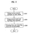
- FIG. 2 shows a flowchart of a lens manufacturing method according to another embodiment of the present invention
- FIGs. 3A to 3F show the lens manufacturing method according to another embodiment of the present invention.
- FIG. 4 shows a cross-sectional view of a light emitting device package according to yet another embodiment of the present invention.
- the dimension of thickness is enlarged in the accompanying drawings to clearly represent several layers and regions.
- the thickness ratio of respective layers shown in the drawings is not necessarily a real thickness ratio.
- a portion such as a layer, a film, a region and a plate is formed or disposed "on" the other portion, it should be understood that the portion may be formed directly on the other portion through a direct contact, or another portion may be disposed therebetween.
- a lens according to the present invention has metal leads formed at the lower end of the lens to use surface mount technology (SMT). Accordingly, the lens can be quickly and easily fixed on a substrate having a light emitting device formed thereon through the metal leads.
- SMT surface mount technology
- FIGs. 1A to 1E show cross-sectional views of the lens according to an embodiment of the present invention.
- the lens according to the embodiment of the present invention will be described with reference to FIGs. 1A to 1E.
- the lens according to the embodiment of the present invention includes a refractive portion 110 and surface mount portions 120.
- a portion of the surface mount portions 120 is formed inside the refractive portion 110.
- the refractive portion 110 is formed of the same material in the same shape as a general lens.
- the refractive portion 110 refracts incident light to change a light path and transmit the light.
- the refractive portion 110 may be formed of thermosetting resin such as silicone, epoxy, PC and PMMA or thermoplastic resin. Further, the refractive portion 110 may be formed of resin for a processing of fixing the surface mount portions 120 as will be described below.
- the refractive portion 110 may be formed in a different shape capable of refracting a path of the incident light.
- the refractive portion 110 may be formed in a spherical or aspherical shape, or in a shape having sectional curvature or bisectional curvature, preferably, having at least one curvature.
- Each of the surface mount portions 120 includes a first part 120b and a second part 120a.
- the second part 120a is fixed into the refractive portion 110 and the first part 120b is fixed on the substrate and the like to fix the refractive portion 110.
- at least one surface mount portion may be disposed. As the number of the surface mount portions increases, the lens can be firmly fixed on the substrate, but the cost may increase.
- the surface mount portion 120 is a device for mounting a part on the substrate as one example of a surface mount device (SMD).
- the surface mount portion 120 includes the first part 120b and the second part 120a.
- the second part 120a is fixed into the refractive portion 110 and may be fixed into the refractive portion 110 through a resin hardening process or the like, as will be described below.
- the first part 120b is exposed to the outside of the refractive portion 110 and may be fixed on the substrate through a light emitting device manufacturing process.
- the surface mount portion 120 may be formed of one metal selected from a group consisting of Au, Ag, Cu and Al. Further, although the surface mount portion 120 is represented in a ' ' shape, the surface mount portion 120 may have any shape capable of fixing the part on the substrate, for example, ' ⁇ ', ⁇ ' , ' ' and ' ⁇ ' as shown in FIGs. 1B to 1E.
- the lens according to the embodiment of the present invention can be fixed on the substrate with the surface mount portions through a simple process.
- FIG. 2 shows a flowchart of a lens manufacturing method according to another embodiment of the present invention.
- FIGs. 3A to 3F show the lens manufacturing method according to another embodiment of the present invention. The lens manufacturing method according to another embodiment of the present invention will be described with reference to FIGs. 2 to 3F.
- the method includes a step of preparing surface mount portions and fixing the surface mount portions to a lens. Specifically, as shown in FIG. 2, the method includes a step S210 of fixing surface mount portions on first molds, a step S220 of fixing a second mold on the first molds with the surface mount portions and injecting a lens material into the second mold, and a step S230 of processing the lens material to form a lens and removing the first and second molds.
- surface mount portions 310 and first molds 300a and 300b are prepared.
- the surface mount portions 310 are provided as a pair of surface mount portions in a shape similar to ' ' in FIG. 3A, at least one surface mount portion may be disposed.
- the surface mount portions 310 are formed of metal such as Au, Ag, Cu and Al.
- the surface mount portions 310 may be formed of any material capable of fixing the lens to the substrate.
- the surface mount portions 310 are bent in a ' ' shape such that they can be easily fixed on the first molds 300a and 300b, the lens, and substrate as will be described below.
- the surface mount portions 310 may have another shape such as ' ⁇ ' , ⁇ ', ' 2' and ' ⁇ ' as well as the ' ', shape.
- Each of the surface mount portions 310 includes a second part to be fixed on the lens and a first part to be fixed on the substrate.
- the first molds 300a and 300b are provided as a pair of first molds in a hexahedral shape as shown in FIG. 3A.
- the first molds 300a and 300b are not necessarily formed in a hexahedral shape and it is sufficient if the process of fixing the surface mount portions can be performed with two first molds.
- the first molds 300a and 300b may be formed of any material capable of fixing the surface mount portions 310.
- the surface mount portions 310 are fixed on the first molds 300a and 300b.
- the surface mount portions 310 are firmly fixed in a space formed in the first molds 300a and 300b.
- the first molds 300a and 300b must not melt to mix with the surface mount portions 310 formed of Au, Ag, Cu, Al, or the like.
- a left portion 300a and a right portion 300b of the first molds are put together to fix the surface mount portions 310 in an inner space. That is, in FIG. 3B, the surface mount portions 310 are fixed in the first molds, and the surface mount portions 310 are surrounded by the first mold 300a such that they are not shown at the outside.
- a second mold 320 is fixed on the first molds 300a and 300b with the surface mount portions 310 fixed thereon, and a lens material 325' is injected into the second mold 320.
- the lens material 325' may be formed of thermosetting resin such as silicone, epoxy, PC and PMMA or thermoplastic resin. In this case, the second mold 320 should not mix with the lens material 325'.
- the second mold 320 is formed on the first molds 300a and 300b with the surface mount portions 310 fixed thereon.
- the second mold 320 is represented as a hexahedron having an empty space 325 of a hemispherical shape.
- the lens material is injected into the empty space 325 to form a lens.
- the empty space 325 may be formed differently according to the shape of a lens to be formed.
- the second mold 320 is fixed on the first molds 300a and 300b such that the lens material is injected into the empty space 325 as will be described below.
- the surface mount portions 310 should be positioned in the empty space 325 inside the second mold 320.
- the lens material 325' is injected into the second mold 320. Since the lens material 325' is injected through the first molds 300a and 300b and the second mold 320, a passage for injecting the lens material is disposed in the first molds or the second mold. The lens material 325' is injected with fluidity and fills the inner space of the second mold 320. When the process of injecting the lens material 325' is completed, the surface mount portions 310 are positioned in the lens material 325'.
- the lens material 325' is processed through a hardening process of cooling the lens material 325' to form a lens.
- a portion of the surface mount portions 310 should be firmly fixed into the lens and the first and second molds should be easily separated from the lens.
- the lens is completed. That is, the surface mount portions 310 are formed in the completed lens 325'.
- the number and shape of the surface mount portions 310 may vary if they can fix the lens to the substrate.
- a portion referred to as a "lens” is equal to a portion referred to as a "refractive portion” in the above embodiment of the lens.
- the lens material 325' is hardened to fix the surface mount portions 310.
- the surface mount portions 310 may be formed in a screw shape and the screw-shaped surface mount portions 310 may be inserted and fixed into the lens.
- the lens manufactured by the lens manufacturing method according to the embodiment of the present invention may be easily and firmly fixed on the substrate or the like through the surface mount portions.
- FIG. 4 shows a cross-sectional view of a light emitting device package according to yet another embodiment of the present invention.
- the light emitting device package according to yet another embodiment of the present invention will be described with reference to FIG. 4.
- the light emitting device package with the above-described lens includes a light emitting portion 410 formed on a substrate 400 and the lens 325' fixed on the substrate 400 through the surface mount portions 310.
- the substrate (printed circuit board; PCB) 400 includes a circuit for driving a light emitting device and the like and the surface mount portions 310 are fixed on the substrate 400.
- the substrate 400 may be formed of a semiconductor material such as Si, ceramic or a resin material.
- the substrate 400 may include a single layer made of the above-mentioned material or multiple layers. In this case, the respective layers may be formed of the same material or different materials.
- the material of the substrate 400 may be patterned by an etching method or the like.
- the respective layers that have been patterned may be stacked.
- the first parts 310b of the surface mount portions 310 are fixed on the surface of the substrate 400 in FIG. 4, the first parts 310b may be inserted and fixed into the substrate 400. Further, the second parts 310a of the surface mount portions 310 are fixed on the lens 325'. Further, since the light emitting portion 410 is surrounded by the lens 325', light emitted from the light emitting portion 410 is refracted through the lens 325' and then emitted to the outside while a light path is changed. Although the light emitting portion 410 is surrounded by the lens 325', it is represented in a different way in FIG. 4.
- the surface mount portions 310 are formed of Au, Ag, Cu, Al or the like.
- the lens 325' may be formed of thermosetting resin such as silicone, epoxy, PC and PMMA or thermoplastic resin. Further, as described above, the surface mount portions 310 are formed in a shape of ' ⁇ ', ' ⁇ ', ' ', ' ⁇ ' , ' ' or the like.
- the light emitting portion 410 is formed on the substrate 400 while being in contact with the substrate 400 in FIG. 4, the light emitting portion 410 may be formed while be spaced from the substrate 400. Further, in order to position the light emitting portion 410 in the lens 325' as shown in FIG. 4, a space for the light emitting portion 410 should be formed in the lens 325'.
- a protruded portion may be formed at a central portion of the first mold to form an empty space at the center of the lens.
- the lens 325' is represented in a hemispherical shape, the lens 325' may be formed in a spherical or aspherical shape, or in a shape having sectional curvature or bisectional curvature, preferably, having at least one curvature.
- the lens 325' should be fixed on the substrate 400 through the surface mount portions 310.
- two surface mount portions 310 are shown in FIG. 4, at least one surface mount portions may be disposed as described above.
- the light emitting portion 410 should be a device capable of emitting light, for example, a light emitting diode (LED).
- the light emitting device package according to the embodiment of the present invention has the following effects.
- the lens Since the lens is fixed on the substrate through the surface mount portions in the above embodiments, the lens can be fixed without using an adhesive differently from a conventional case. Thus, the lens is accurately and firmly fixed at a specified position on the substrate to refract light emitted from the light emitting portion, thereby emitting light at a designed angle.
- the light emitting device and lens can be arranged accurately on the substrate. Also, the light emitting device and lens can be easily and inexpensively arranged on the substrate.
Landscapes
- Physics & Mathematics (AREA)
- General Physics & Mathematics (AREA)
- Optics & Photonics (AREA)
- Led Device Packages (AREA)
- Mounting And Adjusting Of Optical Elements (AREA)
Abstract
Description
- The present invention relates to a lens and a manufacturing method thereof. It more particularly relates to a lens and a light emitting device package formed by introducing surface mount technology (SMT).
- Along with the development of fields using light, parts using optical materials have been widely used in an optical communication device, an optical storage device, medical optical equipment and the like in various industrial fields. The parts using optical materials include a commonly-used lens, a prism, a beam splitter, a reflection mirror and a diffraction grating.
- In the parts using optical materials, the lens is classified into a spherical lens, an aspherical lens, a ball lens, a GRIN lens and the like. Also, the lens is classified into an epoxy lens, a glass lens, a silicone lens and the like according to a material of the lens. Recently, a technology is being developed for a small-sized lens, a lightweight lens, a high-performance lens, and a lens having a large aperture. Particularly, along with the development of a light emitting diode (LED) industry, the demand and requirement for camera flash lenses of portable phones and lenses of LCD products using LED backlight sources are increasing.
- Although the glass lens has high chemical and heat resistance, molding of the glass lens is complicated and expensive compared to molding of polymeric materials. Thus, a method of manufacturing glass by molding polymeric materials has been widely used.
- Further, an injection molding method using a mold is widely used as a method of manufacturing a lens. In the injection molding method, a viscous fluid such as silicone gel or epoxy is injected into the mold and then molded, and the mold is separated, thereby manufacturing a lens. The lens manufactured by the above-mentioned method is installed at a specified position of a device having a light emitting device such as a light emitting diode or a laser diode. The lens refracts light emitted from the light emitting device to change a light path.
- In a conventional method, solder cream having high electric and heat conductivity are formed at portions of light emitting devices of PCB by patterning solder cream only at desired positions using a mask. Electronic devices such as light emitting diodes and Zener diodes are arranged and positioned on the solder cream pattern. The solder cream is heated to a temperature higher than its melting point and cooled down and, thus, electric and optical devices and the metal pattern of PCB are electrically and mechanically connected. That is, after the electric and optical devices are connected, epoxy with high adhesivity is bonded to a portion for mounting a lens, and the lens is mounted on the portion with epoxy by a transfer device. Then, when heating to an appropriate temperature and cooling, the lens is bonded to PCB through epoxy.
- However, the bonding process needs to use epoxy capable of bonding at a temperature less than the melting point of the solder cream. Accordingly, there is a limit in selecting the epoxy and solder cream. Since the electric and optical devices are connected and the lens is bonded, the processing time increases. Also, since the light emitting devices are connected to PCB and the lens is bonded after increasing the temperature, the PCB may become twisted. Thus, it is impossible to accurately arrange the light emitting devices and lens and the unit cost increases.
- Accordingly, the present invention is directed to an improved lens, a manufacturing method thereof and a light emitting device package using the same.
- Embodiments of the present invention can provide a method of accurately arranging a light emitting device and a lens on a substrate.
- Embodiments of the present invention can provide a method of arranging a light emitting device and a lens on a substrate by a simple process and with the inexpensive cost.
- Additional advantages and features of the invention will be set forth in part in the description which follows and in part will become apparent to those having ordinary skill in the art upon examination of the following or may be learned from practice of the invention. The advantages of the invention may be realized and attained by the structure particularly pointed out in the written description and claims hereof as well as the appended drawings.
- In accordance with a first aspect of the invention, a lens includes a refractive portion which refracts incident light; and at least one surface mount portion, wherein a portion of the surface mount portion is formed in the refractive portion.
- In accordance with another aspect of the present invention, there is provided a method of manufacturing a lens comprising preparing at least one surface mount portion; and forming a lens in a region including a portion of the surface mount portion.
- In accordance with yet another aspect of the present invention, there is provided a light emitting device package comprising a substrate with a light emitting device; a lens which refracts light emitted from the light emitting device and transmits the light; and at least one surface mount portion which fixes the lens on the substrate.
- It is to be understood that both the foregoing general description and the following detailed description of the present invention are exemplary and explanatory and are intended to provide further explanation of the invention as claimed.
- The accompanying drawings, which are included to provide a further understanding of the invention and are incorporated in and constitute a part of this application, illustrate embodiment(s) of the invention and together with the description serve to explain the principle of the invention. In the drawings:
- FIGs. 1A to 1E show cross-sectional views of a lens according to an embodiment of the present invention;
- FIG. 2 shows a flowchart of a lens manufacturing method according to another embodiment of the present invention;
- FIGs. 3A to 3F show the lens manufacturing method according to another embodiment of the present invention; and
- FIG. 4 shows a cross-sectional view of a light emitting device package according to yet another embodiment of the present invention.
- Reference will now be made in detail to the preferred embodiments of the present invention, examples of which are illustrated in the accompanying drawings. Wherever possible, the same reference numbers will be used throughout the drawings to refer to the same or like parts.
- Hereinafter, an embodiment of the present invention will be described in detail with reference to the accompanying drawings.
- The dimension of thickness is enlarged in the accompanying drawings to clearly represent several layers and regions. The thickness ratio of respective layers shown in the drawings is not necessarily a real thickness ratio. Meanwhile, when a portion such as a layer, a film, a region and a plate is formed or disposed "on" the other portion, it should be understood that the portion may be formed directly on the other portion through a direct contact, or another portion may be disposed therebetween.
- A lens according to the present invention has metal leads formed at the lower end of the lens to use surface mount technology (SMT). Accordingly, the lens can be quickly and easily fixed on a substrate having a light emitting device formed thereon through the metal leads.
- FIGs. 1A to 1E show cross-sectional views of the lens according to an embodiment of the present invention. The lens according to the embodiment of the present invention will be described with reference to FIGs. 1A to 1E.
- The lens according to the embodiment of the present invention includes a
refractive portion 110 andsurface mount portions 120. A portion of thesurface mount portions 120 is formed inside therefractive portion 110. Preferably, therefractive portion 110 is formed of the same material in the same shape as a general lens. Therefractive portion 110 refracts incident light to change a light path and transmit the light. Therefractive portion 110 may be formed of thermosetting resin such as silicone, epoxy, PC and PMMA or thermoplastic resin. Further, therefractive portion 110 may be formed of resin for a processing of fixing thesurface mount portions 120 as will be described below. Further, although therefractive portion 110 is represented in a hemispherical shape, therefractive portion 110 may be formed in a different shape capable of refracting a path of the incident light. Specifically, therefractive portion 110 may be formed in a spherical or aspherical shape, or in a shape having sectional curvature or bisectional curvature, preferably, having at least one curvature. - Each of the
surface mount portions 120 includes afirst part 120b and asecond part 120a. Thesecond part 120a is fixed into therefractive portion 110 and thefirst part 120b is fixed on the substrate and the like to fix therefractive portion 110. Further, although twosurface mount portions 120 are provided in FIG. 1, at least one surface mount portion may be disposed. As the number of the surface mount portions increases, the lens can be firmly fixed on the substrate, but the cost may increase. - The
surface mount portion 120 is a device for mounting a part on the substrate as one example of a surface mount device (SMD). In this embodiment, thesurface mount portion 120 includes thefirst part 120b and thesecond part 120a. Thesecond part 120a is fixed into therefractive portion 110 and may be fixed into therefractive portion 110 through a resin hardening process or the like, as will be described below. Further, thefirst part 120b is exposed to the outside of therefractive portion 110 and may be fixed on the substrate through a light emitting device manufacturing process. - The
surface mount portion 120 may be formed of one metal selected from a group consisting of Au, Ag, Cu and Al. Further, although thesurface mount portion 120 is represented in a '' shape, the
surface mount portion 120 may have any shape capable of fixing the part on the substrate, for example, '┐', `└' , '' and '↓' as shown in FIGs. 1B to 1E.
- The lens according to the embodiment of the present invention can be fixed on the substrate with the surface mount portions through a simple process.
- FIG. 2 shows a flowchart of a lens manufacturing method according to another embodiment of the present invention. FIGs. 3A to 3F show the lens manufacturing method according to another embodiment of the present invention. The lens manufacturing method according to another embodiment of the present invention will be described with reference to FIGs. 2 to 3F.
- The method includes a step of preparing surface mount portions and fixing the surface mount portions to a lens. Specifically, as shown in FIG. 2, the method includes a step S210 of fixing surface mount portions on first molds, a step S220 of fixing a second mold on the first molds with the surface mount portions and injecting a lens material into the second mold, and a step S230 of processing the lens material to form a lens and removing the first and second molds.
- First,
surface mount portions 310 andfirst molds surface mount portions 310 are provided as a pair of surface mount portions in a shape similar to '' in FIG. 3A, at least one surface mount portion may be disposed. As the number of the surface mount portions increases, there is an advantage in fixing the lens, but there is a problem such as an increase in the cost. The
surface mount portions 310 are formed of metal such as Au, Ag, Cu and Al. Thesurface mount portions 310 may be formed of any material capable of fixing the lens to the substrate. Thesurface mount portions 310 are bent in a '' shape such that they can be easily fixed on the
first molds surface mount portions 310 may have another shape such as '┐' , `└', '2' and '↓' as well as the ' ', shape.
- Each of the
surface mount portions 310 includes a second part to be fixed on the lens and a first part to be fixed on the substrate. Further, thefirst molds first molds first molds surface mount portions 310. - Then, as shown in FIG. 3B, the
surface mount portions 310 are fixed on thefirst molds surface mount portions 310 are firmly fixed in a space formed in thefirst molds first molds surface mount portions 310, there is a problem in the following separation process. Accordingly, thefirst molds surface mount portions 310 formed of Au, Ag, Cu, Al, or the like. In FIG. 3B, aleft portion 300a and aright portion 300b of the first molds are put together to fix thesurface mount portions 310 in an inner space. That is, in FIG. 3B, thesurface mount portions 310 are fixed in the first molds, and thesurface mount portions 310 are surrounded by thefirst mold 300a such that they are not shown at the outside. - Then, as shown in FIGS. 3C and 3D, a
second mold 320 is fixed on thefirst molds surface mount portions 310 fixed thereon, and a lens material 325' is injected into thesecond mold 320. The lens material 325' may be formed of thermosetting resin such as silicone, epoxy, PC and PMMA or thermoplastic resin. In this case, thesecond mold 320 should not mix with the lens material 325'. - First, as shown in FIG. 3C, the
second mold 320 is formed on thefirst molds surface mount portions 310 fixed thereon. In FIG. 3C, thesecond mold 320 is represented as a hexahedron having anempty space 325 of a hemispherical shape. The lens material is injected into theempty space 325 to form a lens. Accordingly, theempty space 325 may be formed differently according to the shape of a lens to be formed. Further, thesecond mold 320 is fixed on thefirst molds empty space 325 as will be described below. Further, thesurface mount portions 310 should be positioned in theempty space 325 inside thesecond mold 320. - Then, as shown in FIG. 3D, the lens material 325' is injected into the
second mold 320. Since the lens material 325' is injected through thefirst molds second mold 320, a passage for injecting the lens material is disposed in the first molds or the second mold. The lens material 325' is injected with fluidity and fills the inner space of thesecond mold 320. When the process of injecting the lens material 325' is completed, thesurface mount portions 310 are positioned in the lens material 325'. - Further, the lens material 325' is processed through a hardening process of cooling the lens material 325' to form a lens. In this case, a portion of the
surface mount portions 310 should be firmly fixed into the lens and the first and second molds should be easily separated from the lens. - Then, when the first and second molds are removed, as shown in FIG. 3E, the lens is completed. That is, the
surface mount portions 310 are formed in the completed lens 325'. Although a pair of ''-shaped
surface mount portions 310 is shown in FIG. 3E, the number and shape of thesurface mount portions 310 may vary if they can fix the lens to the substrate. In this embodiment, a portion referred to as a "lens" is equal to a portion referred to as a "refractive portion" in the above embodiment of the lens. - After the
surface mount portions 310 are positioned in the lens material 325', the lens material 325' is hardened to fix thesurface mount portions 310. However, as shown in FIG. 3F, thesurface mount portions 310 may be formed in a screw shape and the screw-shapedsurface mount portions 310 may be inserted and fixed into the lens. - The lens manufactured by the lens manufacturing method according to the embodiment of the present invention may be easily and firmly fixed on the substrate or the like through the surface mount portions.
- FIG. 4 shows a cross-sectional view of a light emitting device package according to yet another embodiment of the present invention. The light emitting device package according to yet another embodiment of the present invention will be described with reference to FIG. 4.
- The light emitting device package with the above-described lens includes a
light emitting portion 410 formed on asubstrate 400 and the lens 325' fixed on thesubstrate 400 through thesurface mount portions 310. The substrate (printed circuit board; PCB) 400 includes a circuit for driving a light emitting device and the like and thesurface mount portions 310 are fixed on thesubstrate 400. Further, if thesubstrate 400 is formed of silver or white epoxy-based PSR resin or the like, it is possible to increase reflectivity of the light emitting device package. Further, thesubstrate 400 may be formed of a semiconductor material such as Si, ceramic or a resin material. Thesubstrate 400 may include a single layer made of the above-mentioned material or multiple layers. In this case, the respective layers may be formed of the same material or different materials. When thesubstrate 400 is formed of the same material, the material of thesubstrate 400 may be patterned by an etching method or the like. When thesubstrate 400 is formed of different materials, the respective layers that have been patterned may be stacked. - Although the
first parts 310b of thesurface mount portions 310 are fixed on the surface of thesubstrate 400 in FIG. 4, thefirst parts 310b may be inserted and fixed into thesubstrate 400. Further, thesecond parts 310a of thesurface mount portions 310 are fixed on the lens 325'. Further, since thelight emitting portion 410 is surrounded by the lens 325', light emitted from thelight emitting portion 410 is refracted through the lens 325' and then emitted to the outside while a light path is changed. Although thelight emitting portion 410 is surrounded by the lens 325', it is represented in a different way in FIG. 4. - The
surface mount portions 310 are formed of Au, Ag, Cu, Al or the like. The lens 325' may be formed of thermosetting resin such as silicone, epoxy, PC and PMMA or thermoplastic resin. Further, as described above, thesurface mount portions 310 are formed in a shape of '┐', '└', '', '↓' , ' ' or the like.
- Further, although the
light emitting portion 410 is formed on thesubstrate 400 while being in contact with thesubstrate 400 in FIG. 4, thelight emitting portion 410 may be formed while be spaced from thesubstrate 400. Further, in order to position thelight emitting portion 410 in the lens 325' as shown in FIG. 4, a space for thelight emitting portion 410 should be formed in the lens 325'. Thus, for the manufacture of the lens, in the lens manufacturing method of the above-described embodiment, a protruded portion may be formed at a central portion of the first mold to form an empty space at the center of the lens. Further, although the lens 325' is represented in a hemispherical shape, the lens 325' may be formed in a spherical or aspherical shape, or in a shape having sectional curvature or bisectional curvature, preferably, having at least one curvature. The lens 325' should be fixed on thesubstrate 400 through thesurface mount portions 310. Further, although twosurface mount portions 310 are shown in FIG. 4, at least one surface mount portions may be disposed as described above. Further, thelight emitting portion 410 should be a device capable of emitting light, for example, a light emitting diode (LED). - The light emitting device package according to the embodiment of the present invention has the following effects.
- Since the lens is fixed on the substrate through the surface mount portions in the above embodiments, the lens can be fixed without using an adhesive differently from a conventional case. Thus, the lens is accurately and firmly fixed at a specified position on the substrate to refract light emitted from the light emitting portion, thereby emitting light at a designed angle.
- According to the lens, the manufacturing method thereof and the light emitting device package of the present invention, the light emitting device and lens can be arranged accurately on the substrate. Also, the light emitting device and lens can be easily and inexpensively arranged on the substrate.
- It will be apparent to those skilled in the art that various modifications and variations can be made in the present invention without departing from the scope of the invention. Thus, it is intended that the present invention covers the modifications and variations of this invention provided they come within the scope of the appended claims.
Claims (21)
- A lens comprising:a refractive portion which refracts incident light; andat least one surface mount portion,wherein a portion of the surface mount portion is formed in the refractive portion.
- The lens according to claim 1, wherein the surface mount portion includes a first part exposed to an outside of the refractive portion and a second part fixed in the refractive portion.
- The lens according to claim 2, wherein the second part is hardened with the refractive portion or inserted into the refractive portion in a screw shape to be fixed in the refractive portion.
- The lens according to claim 1, wherein the surface mount portion is formed of a material selected from a group consisting of Au, Ag, Cu and Al.
- The lens according to claim 1, wherein the surface mount portion has a shape of '┐', '└', '', '↓' or '
 '.
'.
- The lens according to claim 1, wherein the refractive portion is formed of thermosetting resin such as silicone, epoxy, PC and PMMA or thermoplastic resin.
- The lens according to claim 1, wherein the refractive portion having at least one curvature is formed in a spherical or aspherical shape, or in a shape having sectional curvature or bisectional curvature.
- A method of manufacturing a lens comprising:preparing at least one surface mount portion; andforming a lens in a region including a portion of the surface mount portion.
- The method according to claim 8, wherein the step of forming a lens in a region including a portion of the surface mount portion includes:fixing a first part of the surface mount portion on a first mold;fixing a second mold on the first mold and injecting a lens material into the second mold; andprocessing the lens material to form the lens and removing the first mold and the second mold.
- The method according to claim 8, wherein the step of preparing at least one surface mount portion includes:preparing at least one surface mount portion having a first part and a second part to be fixed on the lens.
- The method according to claim 9, wherein the first mold is divided into at least two portions, and
the step of fixing a first part of the surface mount portion on a first mold includes coupling the at least two portions while the surface mount portion is disposed at an inside of the first mold. - The method according to claim 9, wherein the lens material is formed of thermosetting resin such as silicone, epoxy, PC and PMMA or thermoplastic resin, and the lens material is processed by cooling the lens material.
- The method according to claim 9, wherein the first mold is formed of metal which is not mixed with Au, Ag, Cu and Al.
- The method according to claim 9, wherein the second mold is formed of metal which does not mix with thermosetting resin such as silicone, epoxy, PC and PMMA or thermoplastic resin.
- A light emitting device package comprising:a substrate with a light emitting device;a lens arranged to refract light emitted from the light emitting device and to transmit the light; andat least one surface mount portion arranged to fix the lens on the substrate.
- The light emitting device package according to claim 15, wherein the light emitting device is a LED.
- The light emitting device package according to claim 15, wherein the surface mount portion includes a first part arranged to be fixed on the substrate and a second part fixed on the lens.
- The light emitting device package according to claim 15, wherein the surface mount portion has a shape of '┐', '└', '', '↓' or '
 '.
'.
- The light emitting device package according to claim 15, wherein the substrate is formed of silicone, ceramic, resin, or white or silver epoxy-based PSR resin.
- The light emitting device package according to claim 15, wherein the substrate includes at least two layers and the respective layers are formed of the same material or different materials.
- The light emitting device package according to claim 15, wherein the lens having at least one curvature is formed in a spherical or aspherical shape, or in a shape having sectional curvature or bisectional curvature.
Applications Claiming Priority (1)
| Application Number | Priority Date | Filing Date | Title |
|---|---|---|---|
| KR1020060094629A KR100774218B1 (en) | 2006-09-28 | 2006-09-28 | Lens, manufacturing method and light emitting device package |
Publications (1)
| Publication Number | Publication Date |
|---|---|
| EP1906221A1 true EP1906221A1 (en) | 2008-04-02 |
Family
ID=38779625
Family Applications (1)
| Application Number | Title | Priority Date | Filing Date |
|---|---|---|---|
| EP07253816A Withdrawn EP1906221A1 (en) | 2006-09-28 | 2007-09-26 | Lens, manufacturing method thereof, and light emitting device package using the same |
Country Status (5)
| Country | Link |
|---|---|
| US (2) | US7733573B2 (en) |
| EP (1) | EP1906221A1 (en) |
| JP (1) | JP2008085347A (en) |
| KR (1) | KR100774218B1 (en) |
| TW (1) | TW200824159A (en) |
Families Citing this family (5)
| Publication number | Priority date | Publication date | Assignee | Title |
|---|---|---|---|---|
| JP5292184B2 (en) * | 2009-05-26 | 2013-09-18 | 株式会社東芝 | Optical module and manufacturing method thereof |
| KR101224108B1 (en) | 2010-04-27 | 2013-02-19 | 주식회사 우리조명지주 | Light emitting device and method of manufacturing the same |
| US8789744B2 (en) | 2010-10-19 | 2014-07-29 | Philip Premysler | Reflow solderable, surface mount optic mounting |
| KR101199022B1 (en) * | 2010-12-06 | 2012-11-08 | 엘이디라이텍(주) | Lens unit for LED and LED module using the same |
| KR102340515B1 (en) * | 2015-11-02 | 2021-12-16 | 엘지전자 주식회사 | Backlight unit and display apparatus comprising the same |
Citations (15)
| Publication number | Priority date | Publication date | Assignee | Title |
|---|---|---|---|---|
| JPS5619685A (en) * | 1979-07-25 | 1981-02-24 | Nec Home Electronics Ltd | Manufacture of lens cap for optical semiconductor |
| JPS56152274A (en) * | 1980-04-26 | 1981-11-25 | Nec Home Electronics Ltd | Manufacture of lens cap for photosemiconductor |
| JPS58186980A (en) * | 1982-04-26 | 1983-11-01 | Nec Corp | Photosemiconductor |
| EP0632511A2 (en) * | 1993-06-29 | 1995-01-04 | MITSUBISHI CABLE INDUSTRIES, Ltd. | A light emitting diode aggregate module and a method for manufacturing a light emitting diode aggregate module |
| JPH07221349A (en) * | 1994-01-28 | 1995-08-18 | Shinko Electric Ind Co Ltd | Airtight glass lens cap |
| JPH10242526A (en) * | 1997-02-21 | 1998-09-11 | Citizen Electron Co Ltd | Surface mount type light emitting diode and method of manufacturing the same |
| JP2000252524A (en) * | 1999-02-25 | 2000-09-14 | Citizen Electronics Co Ltd | Surface mount type light emitting diode and method of manufacturing the same |
| JP2003163382A (en) * | 2001-11-29 | 2003-06-06 | Matsushita Electric Ind Co Ltd | Light receiving element or light emitting element package |
| US6614602B1 (en) * | 2002-04-18 | 2003-09-02 | Light Sources, Inc. | Method of manufacturing lens cap for transistor outline package |
| JP2003258352A (en) * | 2002-02-28 | 2003-09-12 | Shinko Electric Ind Co Ltd | Manufacturing method of lens cap |
| US20040183081A1 (en) * | 2003-03-20 | 2004-09-23 | Alexander Shishov | Light emitting diode package with self dosing feature and methods of forming same |
| JP2005005437A (en) * | 2003-06-11 | 2005-01-06 | Seiko Epson Corp | Light emitting element, lighting device, projection display device |
| US20050045903A1 (en) * | 2003-08-29 | 2005-03-03 | Tomoaki Abe | Surface-mounted light-emitting diode and method |
| US20050242708A1 (en) * | 2004-04-30 | 2005-11-03 | Keong Chong C | LED device with a vertical leadframe that is configured for surface mounting |
| US20060006401A1 (en) * | 2004-07-08 | 2006-01-12 | Hsing Chen | Flip chip light emitting diode |
Family Cites Families (11)
| Publication number | Priority date | Publication date | Assignee | Title |
|---|---|---|---|---|
| US6525386B1 (en) * | 1998-03-10 | 2003-02-25 | Masimo Corporation | Non-protruding optoelectronic lens |
| US7290875B2 (en) * | 2004-11-02 | 2007-11-06 | Blum Ronald D | Electro-active spectacles and method of fabricating same |
| US6552368B2 (en) * | 2000-09-29 | 2003-04-22 | Omron Corporation | Light emission device |
| JP2002270888A (en) | 2001-03-08 | 2002-09-20 | Sanyo Electric Co Ltd | Optical semiconductor device |
| US7244965B2 (en) * | 2002-09-04 | 2007-07-17 | Cree Inc, | Power surface mount light emitting die package |
| JP3719431B2 (en) * | 2002-09-25 | 2005-11-24 | セイコーエプソン株式会社 | OPTICAL COMPONENT, ITS MANUFACTURING METHOD, DISPLAY DEVICE, AND IMAGING ELEMENT |
| JP2004271702A (en) | 2003-03-06 | 2004-09-30 | Seiko Epson Corp | Optical component and its manufacturing method, microlens substrate, display device, imaging device, optical device, optical module |
| US7279724B2 (en) * | 2004-02-25 | 2007-10-09 | Philips Lumileds Lighting Company, Llc | Ceramic substrate for a light emitting diode where the substrate incorporates ESD protection |
| TWI241042B (en) * | 2004-03-11 | 2005-10-01 | Chen-Lun Hsingchen | A low thermal resistance LED device |
| TWI277223B (en) * | 2004-11-03 | 2007-03-21 | Chen-Lun Hsingchen | A low thermal resistance LED package |
| KR20070085694A (en) * | 2004-12-03 | 2007-08-27 | 소니 가부시끼가이샤 | Light extraction lens, light emitting element assembly, planar light source device and color liquid crystal display device assembly |
-
2006
- 2006-09-28 KR KR1020060094629A patent/KR100774218B1/en not_active Expired - Fee Related
-
2007
- 2007-09-25 US US11/902,779 patent/US7733573B2/en active Active
- 2007-09-26 EP EP07253816A patent/EP1906221A1/en not_active Withdrawn
- 2007-09-28 JP JP2007254545A patent/JP2008085347A/en not_active Withdrawn
- 2007-09-28 TW TW096136292A patent/TW200824159A/en unknown
-
2010
- 2010-02-19 US US12/709,113 patent/US20100148205A1/en not_active Abandoned
Patent Citations (15)
| Publication number | Priority date | Publication date | Assignee | Title |
|---|---|---|---|---|
| JPS5619685A (en) * | 1979-07-25 | 1981-02-24 | Nec Home Electronics Ltd | Manufacture of lens cap for optical semiconductor |
| JPS56152274A (en) * | 1980-04-26 | 1981-11-25 | Nec Home Electronics Ltd | Manufacture of lens cap for photosemiconductor |
| JPS58186980A (en) * | 1982-04-26 | 1983-11-01 | Nec Corp | Photosemiconductor |
| EP0632511A2 (en) * | 1993-06-29 | 1995-01-04 | MITSUBISHI CABLE INDUSTRIES, Ltd. | A light emitting diode aggregate module and a method for manufacturing a light emitting diode aggregate module |
| JPH07221349A (en) * | 1994-01-28 | 1995-08-18 | Shinko Electric Ind Co Ltd | Airtight glass lens cap |
| JPH10242526A (en) * | 1997-02-21 | 1998-09-11 | Citizen Electron Co Ltd | Surface mount type light emitting diode and method of manufacturing the same |
| JP2000252524A (en) * | 1999-02-25 | 2000-09-14 | Citizen Electronics Co Ltd | Surface mount type light emitting diode and method of manufacturing the same |
| JP2003163382A (en) * | 2001-11-29 | 2003-06-06 | Matsushita Electric Ind Co Ltd | Light receiving element or light emitting element package |
| JP2003258352A (en) * | 2002-02-28 | 2003-09-12 | Shinko Electric Ind Co Ltd | Manufacturing method of lens cap |
| US6614602B1 (en) * | 2002-04-18 | 2003-09-02 | Light Sources, Inc. | Method of manufacturing lens cap for transistor outline package |
| US20040183081A1 (en) * | 2003-03-20 | 2004-09-23 | Alexander Shishov | Light emitting diode package with self dosing feature and methods of forming same |
| JP2005005437A (en) * | 2003-06-11 | 2005-01-06 | Seiko Epson Corp | Light emitting element, lighting device, projection display device |
| US20050045903A1 (en) * | 2003-08-29 | 2005-03-03 | Tomoaki Abe | Surface-mounted light-emitting diode and method |
| US20050242708A1 (en) * | 2004-04-30 | 2005-11-03 | Keong Chong C | LED device with a vertical leadframe that is configured for surface mounting |
| US20060006401A1 (en) * | 2004-07-08 | 2006-01-12 | Hsing Chen | Flip chip light emitting diode |
Also Published As
| Publication number | Publication date |
|---|---|
| TW200824159A (en) | 2008-06-01 |
| KR100774218B1 (en) | 2007-11-08 |
| US20100148205A1 (en) | 2010-06-17 |
| JP2008085347A (en) | 2008-04-10 |
| US20080088953A1 (en) | 2008-04-17 |
| US7733573B2 (en) | 2010-06-08 |
Similar Documents
| Publication | Publication Date | Title |
|---|---|---|
| USRE42112E1 (en) | Chip light emitting diode and fabrication method thereof | |
| EP1959505B1 (en) | LED module with lens and its manufacturing | |
| EP1864780B1 (en) | Apparatus and method for manufacturing a light emitting unit | |
| US7678592B2 (en) | LED housing and fabrication method thereof | |
| US6707125B2 (en) | Solid-state imaging apparatus and manufacturing method thereof | |
| EP2795674B1 (en) | Opto-electronic modules, in particular flash modules, and method for manufacturing the same | |
| KR101944280B1 (en) | Camera Module | |
| US6583444B2 (en) | Semiconductor packages having light-sensitive chips | |
| US7457490B2 (en) | Micro-optics on optoelectronics | |
| TWI601244B (en) | Photovoltaic module and supplies including the same | |
| US10191235B2 (en) | Lens member, method of manufacturing the same, communication module, lens array, and light-source module | |
| US7733573B2 (en) | Lens, manufacturing method thereof and light emitting device package using the same | |
| EP2400569A2 (en) | Light-emitting diode package | |
| WO2003073474A2 (en) | Modular semiconductor die package and method of manufacturing thereof | |
| JP6234036B2 (en) | Optical communication device | |
| EP2802810A1 (en) | Lighting panel | |
| KR20030044884A (en) | Solid-state imaging apparatus and manufacturing method thereof | |
| CN1971320B (en) | Light emitting unit and method of forming the same | |
| US5545359A (en) | Method of making a plastic molded optoelectronic interface | |
| US20090014913A1 (en) | Method for fabricating lens of light emitting diode and device thereof | |
| CN112997313A (en) | Sensor module | |
| US20240310697A1 (en) | Autofocus camera module and manufacturing method therefor, and electronic device having the autofocus camera module | |
| JP4632168B2 (en) | Reflective light emitting device | |
| CN102062879A (en) | Light interrupter | |
| JP2005026503A (en) | Semiconductor light emitting device and manufacturing method thereof |
Legal Events
| Date | Code | Title | Description |
|---|---|---|---|
| PUAI | Public reference made under article 153(3) epc to a published international application that has entered the european phase |
Free format text: ORIGINAL CODE: 0009012 |
|
| AK | Designated contracting states |
Kind code of ref document: A1 Designated state(s): AT BE BG CH CY CZ DE DK EE ES FI FR GB GR HU IE IS IT LI LT LU LV MC MT NL PL PT RO SE SI SK TR |
|
| AX | Request for extension of the european patent |
Extension state: AL BA HR MK YU |
|
| 17P | Request for examination filed |
Effective date: 20081002 |
|
| AKX | Designation fees paid |
Designated state(s): DE FR GB NL |
|
| 17Q | First examination report despatched |
Effective date: 20090917 |
|
| STAA | Information on the status of an ep patent application or granted ep patent |
Free format text: STATUS: THE APPLICATION HAS BEEN WITHDRAWN |
|
| 18W | Application withdrawn |
Effective date: 20111017 |