EP1902472B1 - Semiconductor device comprising a superlattice dielectric interface layer - Google Patents
Semiconductor device comprising a superlattice dielectric interface layer Download PDFInfo
- Publication number
- EP1902472B1 EP1902472B1 EP06752162A EP06752162A EP1902472B1 EP 1902472 B1 EP1902472 B1 EP 1902472B1 EP 06752162 A EP06752162 A EP 06752162A EP 06752162 A EP06752162 A EP 06752162A EP 1902472 B1 EP1902472 B1 EP 1902472B1
- Authority
- EP
- European Patent Office
- Prior art keywords
- semiconductor
- superlattice
- dielectric layer
- monolayer
- monolayers
- Prior art date
- Legal status (The legal status is an assumption and is not a legal conclusion. Google has not performed a legal analysis and makes no representation as to the accuracy of the status listed.)
- Expired - Lifetime
Links
Images



Classifications
-
- H—ELECTRICITY
- H10—SEMICONDUCTOR DEVICES; ELECTRIC SOLID-STATE DEVICES NOT OTHERWISE PROVIDED FOR
- H10D—INORGANIC ELECTRIC SEMICONDUCTOR DEVICES
- H10D62/00—Semiconductor bodies, or regions thereof, of devices having potential barriers
- H10D62/80—Semiconductor bodies, or regions thereof, of devices having potential barriers characterised by the materials
- H10D62/81—Semiconductor bodies, or regions thereof, of devices having potential barriers characterised by the materials of structures exhibiting quantum-confinement effects, e.g. single quantum wells; of structures having periodic or quasi-periodic potential variation
- H10D62/815—Semiconductor bodies, or regions thereof, of devices having potential barriers characterised by the materials of structures exhibiting quantum-confinement effects, e.g. single quantum wells; of structures having periodic or quasi-periodic potential variation of structures having periodic or quasi-periodic potential variation, e.g. superlattices or multiple quantum wells [MQW]
- H10D62/8161—Semiconductor bodies, or regions thereof, of devices having potential barriers characterised by the materials of structures exhibiting quantum-confinement effects, e.g. single quantum wells; of structures having periodic or quasi-periodic potential variation of structures having periodic or quasi-periodic potential variation, e.g. superlattices or multiple quantum wells [MQW] potential variation due to variations in composition or crystallinity, e.g. heterojunction superlattices
- H10D62/8162—Semiconductor bodies, or regions thereof, of devices having potential barriers characterised by the materials of structures exhibiting quantum-confinement effects, e.g. single quantum wells; of structures having periodic or quasi-periodic potential variation of structures having periodic or quasi-periodic potential variation, e.g. superlattices or multiple quantum wells [MQW] potential variation due to variations in composition or crystallinity, e.g. heterojunction superlattices having quantum effects only in the vertical direction, i.e. layered structures having quantum effects solely resulting from vertical potential variation
-
- B—PERFORMING OPERATIONS; TRANSPORTING
- B82—NANOTECHNOLOGY
- B82Y—SPECIFIC USES OR APPLICATIONS OF NANOSTRUCTURES; MEASUREMENT OR ANALYSIS OF NANOSTRUCTURES; MANUFACTURE OR TREATMENT OF NANOSTRUCTURES
- B82Y10/00—Nanotechnology for information processing, storage or transmission, e.g. quantum computing or single electron logic
-
- H—ELECTRICITY
- H10—SEMICONDUCTOR DEVICES; ELECTRIC SOLID-STATE DEVICES NOT OTHERWISE PROVIDED FOR
- H10D—INORGANIC ELECTRIC SEMICONDUCTOR DEVICES
- H10D30/00—Field-effect transistors [FET]
- H10D30/60—Insulated-gate field-effect transistors [IGFET]
- H10D30/601—Insulated-gate field-effect transistors [IGFET] having lightly-doped drain or source extensions, e.g. LDD IGFETs or DDD IGFETs
-
- H—ELECTRICITY
- H10—SEMICONDUCTOR DEVICES; ELECTRIC SOLID-STATE DEVICES NOT OTHERWISE PROVIDED FOR
- H10D—INORGANIC ELECTRIC SEMICONDUCTOR DEVICES
- H10D30/00—Field-effect transistors [FET]
- H10D30/60—Insulated-gate field-effect transistors [IGFET]
- H10D30/751—Insulated-gate field-effect transistors [IGFET] having composition variations in the channel regions
-
- H—ELECTRICITY
- H10—SEMICONDUCTOR DEVICES; ELECTRIC SOLID-STATE DEVICES NOT OTHERWISE PROVIDED FOR
- H10D—INORGANIC ELECTRIC SEMICONDUCTOR DEVICES
- H10D62/00—Semiconductor bodies, or regions thereof, of devices having potential barriers
- H10D62/80—Semiconductor bodies, or regions thereof, of devices having potential barriers characterised by the materials
- H10D62/81—Semiconductor bodies, or regions thereof, of devices having potential barriers characterised by the materials of structures exhibiting quantum-confinement effects, e.g. single quantum wells; of structures having periodic or quasi-periodic potential variation
- H10D62/815—Semiconductor bodies, or regions thereof, of devices having potential barriers characterised by the materials of structures exhibiting quantum-confinement effects, e.g. single quantum wells; of structures having periodic or quasi-periodic potential variation of structures having periodic or quasi-periodic potential variation, e.g. superlattices or multiple quantum wells [MQW]
- H10D62/8161—Semiconductor bodies, or regions thereof, of devices having potential barriers characterised by the materials of structures exhibiting quantum-confinement effects, e.g. single quantum wells; of structures having periodic or quasi-periodic potential variation of structures having periodic or quasi-periodic potential variation, e.g. superlattices or multiple quantum wells [MQW] potential variation due to variations in composition or crystallinity, e.g. heterojunction superlattices
- H10D62/8162—Semiconductor bodies, or regions thereof, of devices having potential barriers characterised by the materials of structures exhibiting quantum-confinement effects, e.g. single quantum wells; of structures having periodic or quasi-periodic potential variation of structures having periodic or quasi-periodic potential variation, e.g. superlattices or multiple quantum wells [MQW] potential variation due to variations in composition or crystallinity, e.g. heterojunction superlattices having quantum effects only in the vertical direction, i.e. layered structures having quantum effects solely resulting from vertical potential variation
- H10D62/8164—Semiconductor bodies, or regions thereof, of devices having potential barriers characterised by the materials of structures exhibiting quantum-confinement effects, e.g. single quantum wells; of structures having periodic or quasi-periodic potential variation of structures having periodic or quasi-periodic potential variation, e.g. superlattices or multiple quantum wells [MQW] potential variation due to variations in composition or crystallinity, e.g. heterojunction superlattices having quantum effects only in the vertical direction, i.e. layered structures having quantum effects solely resulting from vertical potential variation comprising only semiconductor materials
-
- H—ELECTRICITY
- H10—SEMICONDUCTOR DEVICES; ELECTRIC SOLID-STATE DEVICES NOT OTHERWISE PROVIDED FOR
- H10D—INORGANIC ELECTRIC SEMICONDUCTOR DEVICES
- H10D64/00—Electrodes of devices having potential barriers
- H10D64/60—Electrodes characterised by their materials
- H10D64/66—Electrodes having a conductor capacitively coupled to a semiconductor by an insulator, e.g. MIS electrodes
- H10D64/68—Electrodes having a conductor capacitively coupled to a semiconductor by an insulator, e.g. MIS electrodes characterised by the insulator, e.g. by the gate insulator
-
- H—ELECTRICITY
- H10—SEMICONDUCTOR DEVICES; ELECTRIC SOLID-STATE DEVICES NOT OTHERWISE PROVIDED FOR
- H10D—INORGANIC ELECTRIC SEMICONDUCTOR DEVICES
- H10D64/00—Electrodes of devices having potential barriers
- H10D64/60—Electrodes characterised by their materials
- H10D64/66—Electrodes having a conductor capacitively coupled to a semiconductor by an insulator, e.g. MIS electrodes
- H10D64/68—Electrodes having a conductor capacitively coupled to a semiconductor by an insulator, e.g. MIS electrodes characterised by the insulator, e.g. by the gate insulator
- H10D64/681—Electrodes having a conductor capacitively coupled to a semiconductor by an insulator, e.g. MIS electrodes characterised by the insulator, e.g. by the gate insulator having a compositional variation, e.g. multilayered
- H10D64/685—Electrodes having a conductor capacitively coupled to a semiconductor by an insulator, e.g. MIS electrodes characterised by the insulator, e.g. by the gate insulator having a compositional variation, e.g. multilayered being perpendicular to the channel plane
-
- H—ELECTRICITY
- H10—SEMICONDUCTOR DEVICES; ELECTRIC SOLID-STATE DEVICES NOT OTHERWISE PROVIDED FOR
- H10D—INORGANIC ELECTRIC SEMICONDUCTOR DEVICES
- H10D84/00—Integrated devices formed in or on semiconductor substrates that comprise only semiconducting layers, e.g. on Si wafers or on GaAs-on-Si wafers
- H10D84/01—Manufacture or treatment
- H10D84/0123—Integrating together multiple components covered by H10D12/00 or H10D30/00, e.g. integrating multiple IGBTs
- H10D84/0126—Integrating together multiple components covered by H10D12/00 or H10D30/00, e.g. integrating multiple IGBTs the components including insulated gates, e.g. IGFETs
- H10D84/0165—Integrating together multiple components covered by H10D12/00 or H10D30/00, e.g. integrating multiple IGBTs the components including insulated gates, e.g. IGFETs the components including complementary IGFETs, e.g. CMOS devices
- H10D84/0167—Manufacturing their channels
-
- H—ELECTRICITY
- H10—SEMICONDUCTOR DEVICES; ELECTRIC SOLID-STATE DEVICES NOT OTHERWISE PROVIDED FOR
- H10D—INORGANIC ELECTRIC SEMICONDUCTOR DEVICES
- H10D84/00—Integrated devices formed in or on semiconductor substrates that comprise only semiconducting layers, e.g. on Si wafers or on GaAs-on-Si wafers
- H10D84/01—Manufacture or treatment
- H10D84/02—Manufacture or treatment characterised by using material-based technologies
- H10D84/03—Manufacture or treatment characterised by using material-based technologies using Group IV technology, e.g. silicon technology or silicon-carbide [SiC] technology
- H10D84/038—Manufacture or treatment characterised by using material-based technologies using Group IV technology, e.g. silicon technology or silicon-carbide [SiC] technology using silicon technology, e.g. SiGe
-
- H—ELECTRICITY
- H10—SEMICONDUCTOR DEVICES; ELECTRIC SOLID-STATE DEVICES NOT OTHERWISE PROVIDED FOR
- H10D—INORGANIC ELECTRIC SEMICONDUCTOR DEVICES
- H10D64/00—Electrodes of devices having potential barriers
- H10D64/60—Electrodes characterised by their materials
- H10D64/66—Electrodes having a conductor capacitively coupled to a semiconductor by an insulator, e.g. MIS electrodes
- H10D64/68—Electrodes having a conductor capacitively coupled to a semiconductor by an insulator, e.g. MIS electrodes characterised by the insulator, e.g. by the gate insulator
- H10D64/691—Electrodes having a conductor capacitively coupled to a semiconductor by an insulator, e.g. MIS electrodes characterised by the insulator, e.g. by the gate insulator comprising metallic compounds, e.g. metal oxides or metal silicates
Definitions
- the present invention relates to the field of semiconductors, and, more particularly, to semiconductors having enhanced properties based upon energy band engineering and associated methods.
- U.S. Patent No. 6,472, 685 B2 to Takagi discloses a semiconductor device including a silicon and carbon layer sandwiched between silicon layers so that the conduction band and valence band of the second silicon layer receive a tensile strain. Electrons having a smaller effective mass, and which have been induced by an electric field applied to the gate electrode, are confined in the second silicon layer, thus, an n-channel MOSFET is asserted to have a higher mobility.
- U.S. Patent No. 4,937,204 to Ishibashi et al discloses a superlattice in which a plurality of layers, less than eight monolayers, and containing a fraction or a binary compound semiconductor layers, are alternately and epitaxially grown. The direction of main current flow is perpendicular to the layers of the superlattice.
- U.S. Patent No. 5,357,119 to Wang et al discloses a Si-Ge short period superlattice with higher mobility achieved by reducing alloy scattering in the superlattice.
- U.S. Patent No. 5,683,934 to Candelaria discloses an enhanced mobility MOSFET including a channel layer comprising an alloy of silicon and a second material substitutionally present in the silicon lattice at a percentage that places the channel layer under tensile stress.
- U.S. Patent No. 5,216,262 to Tsu discloses a quantum well structure comprising two barrier regions and a thin epitaxially grown semiconductor layer sandwiched between the barriers.
- Each barrier region consists of alternate layers of SiO 2 /Si with a thickness generally in a range of two to six monolayers. A much thicker section of silicon is sandwiched between the barriers.
- An article entitled " Phenomena in silicon nanostructure devices" also to Tsu and published online September 6, 2000 by Applied Physics and Materials Science & Processing, pp. 391-402 discloses a semiconductor-atomic superlattice (SAS) of silicon and oxygen.
- the Si/O superlattice is disclosed as useful in a silicon quantum and light-emitting devices.
- a green electromuminescence diode structure was constructed and tested. Current flow in the diode structure is vertical, that is, perpendicular to the layers of the SAS.
- the disclosed SAS may include semiconductor layers separated by adsorbed species such as oxygen atoms, and CO molecules. The silicon growth beyond the adsorbed monolayer of oxygen is described as epitaxial with a fairly low defect density.
- One SAS structure included a 1.1 nm thick silicon portion that is about eight atomic layers of silicon, and another structure had twice this thickness of silicon.
- An article to Luo et al. entitled “Chemical Design of Direct-Gap Light-Emitting Silicon” published in Physical Review Letters, Vol. 89, No. 7 (August 12, 2002 ) further discusses the light emitting SAS structures of Tsu.
- WO 02/103,767 A1 discloses a barrier building block of thin silicon and oxygen, carbon, nitrogen, phosphorous, antimony, arsenic or hydrogen to thereby reduce current flowing vertically through the lattice more than four orders of magnitude.
- the insulating layer/barrier layer allows for low defect epitaxial silicon to be deposited next to the insulating layer.
- APBG Aperiodic Photonic Band-Gap
- material parameters for example, the location of band minima, effective mass, etc, can be tailored to yield new aperiodic materials with desirable band-structure characteristics.
- Other parameters such as electrical conductivity, thermal conductivity and dielectric permittivity or magnetic permeability are disclosed as also possible to be designed into the material.
- a semiconductor device as claimed in claim 1, which includes a semiconductor substrate and at least one active device adjacent the semiconductor substrate. More particularly, the at least one active device includes an electrode layer, a high-K dielectric layer underlying the electrode layer and in contact therewith, and a superlattice underlying the high-K dielectric layer opposite the electrode layer and in contact with the high-K dielectric layer.
- the superlattice includes a plurality of stacked groups of layers. Moreover, each group of layers of the superlattice includes a plurality of stacked base semiconductor monolayers defining a base semiconductor portion and at least one non-semiconductor monolayer constrained within a crystal lattice of adjacent base semiconductor portions.
- a method for manufacturing the device is claimed in claim 15.
- the superlattice advantageously acts as an interface for the high-K dielectric layer which provides reduced scattering and, thus, enhanced mobility with respect to prior art insulation layers such as silicon oxides used with high-K dielectrics. Moreover, use of the superlattice as an insulator for applications using high-K dielectrics may result in smaller overall thicknesses, and thus improved device capacitance.
- the high-K dielectric layer may have a dielectric constant of greater than about five and, more particularly, greater than about ten or twenty, for example. Further, the at least one non-semiconductor monolayer may be less than about five monolayers to thereby function as an energy band-modifying layer.
- the high-K dielectric layer may comprise at least one of silicon oxide, zirconium oxide, and hafnium oxide.
- the at least one active device further includes a channel region underlying the superlattice, as well as source and drain regions adjacent the channel region.
- the base semiconductor may comprise silicon
- the at least one non-semiconductor monolayer may comprise oxygen. More particularly, the at least one non-semiconductor monolayer may be a non-semiconductor selected from the group consisting of oxygen, nitrogen, fluorine, and carbon-oxygen.
- the at least one non-semiconductor monolayer may be a single monolayer thick, and each base semiconductor portion may be less than eight monolayers thick, for example. Furthermore, in some embodiments all of the base semiconductor portions may be a.same number of monolayers thick. In other embodiments, at least some of the base semiconductor portions may be a different number of monolayers thick. Moreover, opposing base semiconductor monolayers in adjacent groups of layers of the superlattice are chemically bound together.
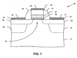
- FIG. 1 is schematic cross-sectional diagram of a semiconductor device in accordance with the present invention including a superlattice.
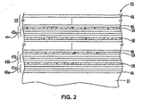
- FIG. 2 is a greatly enlarged schematic cross-sectional view of the superlattice as shown in FIG. 1 .
- FIG. 3 is a perspective schematic atomic diagram of a portion of the superlattice shown in FIG. 1 .
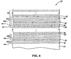
- FIG. 4 is a greatly enlarged schematic cross-sectional view of another embodiment of a superlattice that may be used in the device of FIG. 1 .
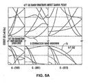
- FIG. 5A is a graph of the calculated band structure from the gamma point (G) for both bulk silicon as in the prior art, and for the 4/1 Si/O superlattice as shown in FIGS. 1-3 .
- FIG. 5B is a graph of the calculated band structure from the Z point for both bulk silicon as in the prior art, and for the 4/1 Si/O superlattice as shown in FIGS. 1-3 .
- FIG. 5C is a graph of the calculated band structure from both the gamma and Z points for both bulk silicon as in the prior art, and for the 5/1/3/1 Si/O superlattice as shown in FIG. 4 .
- FIGS. 6A-6C are a series of schematic cross-sectional diagrams illustrating a method for making the semiconductor device of FIG. 1 .
- the present invention relates to controlling the properties of semiconductor materials at the atomic or molecular level to achieve improved performance within semiconductor devices. Further, the invention relates to the identification, creation, and use of improved, materials for use in the conduction paths of semiconductor devices.
- f is the Fermi-Dirac distribution
- E F is the Fermi energy
- T is the temperature
- E(k,n) is the energy of an electron in the state corresponding to wave vector k and the n th energy band
- the indices i and j refer to Cartesian coordinates x, y and z
- the integrals are taken over the Brillouin zone (B.Z.)
- the summations are taken over bands with energies above and below the Fermi energy for electrons and holes respectively.
- the conductivity reciprocal effective mass tensor is such that a tonsorial component of the conductivity of the material is greater for greater values of the corresponding component of the conductivity reciprocal effective mass tensor.
- the superlattices described herein set the values of the conductivity reciprocal effective mass tensor so as to enhance the conductive properties of the material, such as typically for a preferred direction of charge carrier transport.
- the inverse of the appropriate tensor element is referred to as the conductivity effective mass.
- the conductivity effective mass for electrons/holes as described above and calculated in the direction of intended carrier transport is used to distinguish improved materials.
- One such example would be a superlattice 25 material as a dielectric interface layer in a semiconductor device.
- a planar MOSFET 20 including the superlattice 25 in accordance with the invention is first described with reference to FIG. 1 .
- the materials identified herein could be used in many different types of semiconductor devices, such as discrete devices and/or integrated circuits.
- another application in which the superlattice 25 may be used as a dielectric interface layers is FINFETs.
- the illustrated MOSFET 20 includes a substrate 21, lightly doped source/drain extension regions 22, 23, more heavily doped source/drain regions 26, 27, and a channel region 24 therebetween.
- the superlattice 25 overlies the channel region 24 and is in contact therewith.
- a gate dielectric layer 37 (which is shown with stippling for clarity of illustration in FIG. 1 ) is on the superlattice 25, and a gate electrode layer 36 is on the gate dielectric layer and opposite the superlattice.
- Sidewall spacers 40, 41 are also provided in the illustrated MOSFET 20, as well as silicide layers 30, 31, and 34 on the lightly doped source and drain regions 22, 23 and the gate electrode layer 36, respectively.
- the superlattice 25 advantageously acts as an interface for the gate dielectric layer 37 which provides reduced scattering and, thus, enhanced mobility with respect to prior art insulation layers such as silicon oxides used with high-K dielectrics. Moreover, use of the superlattice 25 as an insulator for applications using high-K dielectrics may result in smaller overall thicknesses, and thus improved device capacitance. This is because the superlattice 25 may be formed in relatively small thicknesses yet still provide desired insulating properties, as will be discussed further below.
- the gate dielectric layer 37 preferably comprises a high-K dielectric having a dielectric constant of greater than about five and, more preferably, greater than about ten or twenty.
- Applicants have identified improved materials or structures for the superlattice 25 of the MOSFET 20. More specifically, the Applicants have identified materials or structures having energy band structures for which the appropriate conductivity effective masses for electrons and/or holes are substantially less than the corresponding values for silicon.
- the materials or structures are in the form of a superlattice 25 whose structure is controlled at the atomic or molecular level and may be formed using known techniques of atomic or molecular layer deposition.
- the superlattice 25 includes a plurality of layer groups 45a-45n arranged in stacked relation, as perhaps best understood with specific reference to the schematic cross-sectional view of FIG. 2 .
- Each group of layers 45a-45n of the superlattice 25 illustratively includes a plurality of stacked base semiconductor monolayers 46 defining a respective base semiconductor portion 46a-46n and an energy band-modifying layer 50 thereon.
- the energy band-modifying layers 50 are indicated by stippling in FIG. 2 for clarity of illustration.
- the energy-band modifying layer 50 illustratively includes one non-semiconductor monolayer constrained within a crystal lattice of adjacent base semiconductor portions. That is, opposing base semiconductor monolayers 46 in adjacent groups of layers 45a-45n are chemically bound together. For example, in the case of silicon monolayers 46, some of the silicon atoms in the upper or top semiconductor monolayer of the group of monolayers 46a will be covalently bonded with silicon atoms in the lower or bottom monolayer of the group 46b. This allows the crystal lattice to continue through the groups of layers despite the presence of the non-semiconductor monolayer(s) (e.g., oxygen monolayer(s)).
- the non-semiconductor monolayer(s) e.g., oxygen monolayer(s)
- more than one non-semiconductor layer monolayer may be possible.
- the number of non-semiconductor monolayers in the energy band-modifying layer 50 may preferably be less than about five monolayers to thereby provide the desired energy band-modifying properties.
- non-semiconductor or semiconductor monolayer means that the material used for the monolayer would be a non-semiconductor or semiconductor if formed in bulk. That is, a single monolayer of a material, such as semiconductor, may not necessarily exhibit the same properties that it would if formed in bulk or in a relatively thick layer, as will be appreciated by those skilled in the art.
- energy band-modifying layers 50 and adjacent base semiconductor portions 46a-46n cause the superlattice 25 to have a lower appropriate conductivity effective mass for the charge carriers in the parallel layer direction than would otherwise be present.
- this parallel direction is orthogonal to the stacking direction.
- the band modifying layers 50 may also cause the superlattice 25 to have a common energy band structure, while also advantageously functioning as an insulator between layers or regions vertically above and below the superlattice.
- this structure may also advantageously act as a barrier to dopant and/or material bleed between layers vertically above and below the superlattice 25.
- These properties may thus advantageously allow the superlattice 25 to provide an interface for high-K dielectrics which not only reduces bleeding of the high-K material into the channel region, but which may also advantageously reduce unwanted scattering effects and improve device mobility, as will be appreciated by those skilled in the art.
- the superlattice 25 may further have a substantially direct energy bandgap that may be particularly advantageous for opto-electronic devices, for example, as described in further detail below.
- the superlattice 25 may only be used for its dopant blocking/insulation properties or its enhanced mobility, or it may be used for both in other applications, as will be appreciated by those skilled in the art.
- the superlattice 25 may also advantageously be used to provide the channel region 24. That is, the illustrated superlattice 25 may be formed of a sufficient thickness so that lower.groups of layers 45 may be used as the channel, while upper groups of layers may provide the high-K dielectric interface. Alternately, respective superlattice layers may be formed for these purposes. Further details on using such a superlattice as a channel in a semiconductor device are provided in U.S. patent application US 2002/262,597 , which is assigned to the present Assignee and is hereby incorporated in its entirety by reference, for example.
- the source/drain regions 22, 23 and gate 35 of the MOSFET 20 may be considered as regions for causing the transport of charge carriers through the superlattice in a parallel direction relative to the layers of the stacked groups 45a-45a. Other such regions are also contemplated by the present invention.
- the superlattice 25 also illustratively includes a cap layer 52 on an upper layer group 45n.
- the cap layer 52 may comprise a plurality of base semiconductor monolayers 46.
- the cap layer 52 may have between 2 to 100 monolayers of the base semiconductor, and, more preferably between 10 to 50 monolayers.
- Each base semiconductor portion 46a-46n may comprise a base semiconductor selected from the group consisting of Group IV semiconductors, Group III-V semiconductors, and Group II-VI semiconductors.
- Group IV semiconductors also includes Group IV-IV semiconductors, as will be appreciated by those skilled in the art.
- the base semiconductor may comprise at least one of silicon and germanium, for example.
- Each energy band-modifying layer 50 may comprise a non-semiconductor selected from the group consisting of oxygen, nitrogen, fluorine, and carbon-oxygen, for example.
- the non-semiconductor is also desirably thermally stable through deposition of a next layer to thereby facilitate manufacturing.
- the non-semiconductor may be another inorganic or organic element or compound that is compatible with the given semiconductor processing as will be appreciated by those skilled in the art.
- the term "monolayer” is meant to include a single atomic layer and also a single molecular layer. It is also noted that the energy band-modifying layer 50 provided by a single monolayer is also meant to include a monolayer wherein not all of the possible sites are occupied. For example, with particular reference to the atomic diagram of FIG. 3 , a 4/1 repeating structure is illustrated for silicon as the base semiconductor material, and oxygen as the energy band-modifying material. Only half of the possible sites for oxygen are occupied.
- this one half occupation would not necessarily be the case as will be appreciated by those skilled in the art. Indeed it can be seen even in this schematic diagram, that individual atoms of oxygen in a given monolayer are not precisely aligned along a flat plane as will also be appreciated by those of skill in the art of atomic deposition.
- a preferred occupation range is from about one-eighth to one-half of the possible oxygen sites being full, although other numbers may be used in certain embodiments.
- Silicon and oxygen are currently widely used in conventional semiconductor processing, and, hence, manufacturers will be readily able to use these materials as described herein.
- Atomic or monolayer deposition is also now widely used. Accordingly, semiconductor devices incorporating the superlattice 25 in accordance with the invention may be readily adopted and implemented, as will be appreciated by those skilled in the art.
- the number of silicon monolayers should desirably be seven or less so that the energy band of the superlattice is common or relatively uniform throughout to achieve the desired advantages.
- the 4/1 repeating structure shown in FIGS. 2 and 3 for Si/O has been modeled to indicate an enhanced mobility for electrons and holes in the X direction.
- the calculated conductivity effective mass for electrons is 0.26 and for the 4/1 SiO superlattice in the X direction it is 0.12 resulting in a ratio of 0.46.
- the calculation for holes yields values of 0.36 for bulk silicon and 0.16 for the 4/1 Si/O superlattice resulting in a ratio of 0.44.
- While such a directionally preferential feature may be desired in certain semiconductor devices, other devices may benefit from a more uniform increase in mobility in any direction parallel to the groups of layers. It may also be beneficial to have an increased mobility for both electrons and holes, or just one of these types of charge carriers as will be appreciated by those skilled in the art.
- the lower conductivity effective mass for the 4/1 Si/O embodiment of the superlattice 25 may be less than two-thirds the conductivity effective mass than would otherwise occur; and this applies for both electrons and holes.
- the superlattice 25 may further comprise at least one type of conductivity dopant therein, as will also be appreciated by those skilled in the art. It may be especially appropriate to dope some portion of the superlattice 25 if the superlattice is to provide a portion of the channel, for example.
- FIG. 4 another embodiment of a superlattice 25' in accordance with the invention having different properties is now described.
- a repeating pattern of 3/1/5/1 is illustrated. More particularly, the lowest base semiconductor portion 46a' has three monolayers, and the second lowest base semiconductor portion 46b' has five monolayers. This pattern repeats throughout the superlattice 25'.
- the energy band-modifying layers 50' may each include a single monolayer.
- the enhancement of charge carrier mobility is independent of orientation in the plane of the layers.
- all of the base semiconductor portions 46a-46n of a superlattice 25 may be a same number of monolayers thick. In other embodiments, at least some of the base semiconductor portions 46a-46n may be a different number of monolayers thick. In still other embodiments, all of the base semiconductor portions 46a-46n may be a different number of monolayers thick.
- FIGS. 5A-5C band structures calculated using Density Functional Theory (DFT) are presented. It is well known in the art that DFT underestimates the absolute value of the bandgap. Hence all bands above the gap may be shifted by an appropriate "scissors correction.” However the shape of the band is known to be much more reliable. The vertical energy axes should be interpreted in this light.
- DFT Density Functional Theory
- FIG. 5A shows the calculated band structure from the gamma point (G) for both bulk silicon (represented by continuous lines) and for the 4/1 Si/O superlattice 25 as shown in FIGS. 1-3 (represented by dotted lines).
- the directions refer to the unit cell of the 4/1 Si/O structure and not to the conventional unit cell of Si, although the (001) direction in the figure does correspond to the (001) direction of the conventional unit cell of Si, and, hence, shows the expected location of the Si conduction band minimum.
- the (100) and (010) directions in the figure correspond to the (110) and (-110) directions of the conventional Si unit cell.
- the bands of Si on the figure are folded to represent them on the appropriate reciprocal lattice directions for the 4/1 Si/O structure.
- the conduction band minimum for the 4/1 Si/O structure is located at the gamma point in contrast to bulk silicon (Si), whereas the valence band minimum occurs at the edge of the Brillouin zone in the (001) direction which we refer to as the Z point.
- the greater curvature of the conduction band minimum for the 4/1 Si/O structure compared to the curvature of the conduction band minimum for Si owing to the band splitting due to the perturbation introduced by the additional oxygen layer.
- FIG. 5B shows the calculated band structure from the Z point for both bulk silicon (continuous lines) and for the 4/1 Si/O superlattice 25 (dotted lines). This figure illustrates the enhanced curvature of the valence band in the (100) direction.
- FIG. 5C shows the calculated band structure from both the gamma and Z point for both bulk silicon (continuous lines) and for the 5/1/3/1 Si/O structure of the superlattice 25' of FIG. 4 (dotted lines). Due to the symmetry of the 5/1/3/1 Si/O structure, the calculated band structures in the (100) and (010) directions are equivalent. Thus the conductivity effective mass and mobility are expected to be isotropic in the plane parallel to the layers, i.e. perpendicular to the (001) stacking direction. Note that in the 5/1/3/1 Si/O example the conduction band minimum and the valence band maximum are both at or close to the Z point.
- the appropriate comparison and discrimination may be made via the conductivity reciprocal effective mass tensor calculation. This leads Applicants to further theorize that the 5/1/3/1 superlattice 25' should be substantially direct bandgap.
- the appropriate matrix element for optical transition is another indicator of the distinction between direct and indirect bandgap behavior.
- the method begins with providing the silicon substrate 21.
- the substrate may be an eight-inch wafer 21 of lightly doped P-type or N-type single crystal silicon with ⁇ 100> orientation, although other suitable substrates may also be used.
- a layer of the superlattice 25 material is then formed across the upper surface of the substrate 21.
- the superlattice 25 material is deposited across the surface of the substrate 21 using atomic layer deposition and the epitaxial silicon cap layer 52 is formed, as discussed previously above, and the surface is planarized. It should be noted that in some embodiments the superlattice 25 material may be selectively deposited in desired areas, rather than across the entire substrate 21, as will be appreciated by those skilled in the art. Moreover, planarization may not be required in all embodiments.
- the epitaxial silicon cap layer 52 may have a preferred thickness to prevent superlattice consumption during gate oxide growth, or any other subsequent oxidations, while at the same time reducing or minimizing the thickness of the silicon cap layer to reduce any parallel path of conduction with the superlattice. According to the well-known relationship of consuming approximately 45% of the underlying silicon for a given oxide grown, the silicon cap layer may be greater than 45% of the grown gate oxide thickness plus a small incremental amount to account for manufacturing tolerances known to those skilled in the art. For the present example, and assuming growth of a 25 angstrom gate, one may use approximately 13-15 angstroms of silicon cap thickness.
- the gate dielectric layer 37 and the gate electrode layer 36 are formed. More particularly, the high-K material is deposited, and steps of poly deposition, patterning, and etching are performed to provide the gate stack illustrated in FIG. 6A .
- Poly deposition refers to low-pressure chemical vapor deposition (LPCVD) of silicon onto an oxide (hence it forms a polycrystalline material). The step includes doping with P+ or As- to make it conducting, and the layer may be around 250 nm thick, for example.
- the pattern step may include performing a spinning photoresist, baking, exposure to light (i.e., a photolithography step), and developing the resist.
- the pattern is then transferred to another layer (oxide or nitride) which acts as an etch mask during the etch step.
- the etch step typically is a plasma etch (anisotropic, dry etch) that is material selective (e.g., etches silicon ten times faster than oxide) and transfers the lithography pattern into the material of interest.
- the superlattice 25 material may be etched using known semiconductor processing techniques. However, it should be noted that with the non-semiconductor present in the superlattice 25, e.g., oxygen, the superlattice may be more easily etched using an etchant formulated for oxides rather than silicon. Of course, the appropriate etch for a given implementation will vary based upon the structure and materials used for the superlattice 25 and substrate 21 , as will be appreciated by those of skill in the art.
- the lightly doped source and drain extensions 22, 23 are formed. These regions are formed using n-type or p-type LDD implantation, annealing, and cleaning. An anneal step may be used after the LDD implantation, but depending on the specific process, it may be omitted.
- the clean step is a chemical etch to remove metals and organics prior to depositing an oxide layer.
- FIG. 6C shows the formation of the sidewall spacers 40, 41 and the source and drain 26, 27 implants.
- An SiO 2 mask may be deposited and etched back for this purpose.
- N-type or p-type ion implantation is used to form the source and drain regions 26, 27, depending upon the given implementation.
- the structure is then annealed and cleaned.
- Self-aligned silicide formation may then be performed to form the silicide layers 30, 31, and 34, and the source/drain contacts 32, 33, are formed to provide the final semiconductor device 20 illustrated in FIG. 1 .
- the silicide formation is also known as salicidation.
- the salicidation process includes metal deposition (e.g., Ti), nitrogen annealing, metal etching, and a second annealing.
- the foregoing is, of course, but one example of a process and device in which the present invention may be used, and those of skill in the art will understand its application and use in many other processes and devices.
- the structures of the present invention may be formed on a portion of a wafer or across substantially all of a wafer.
- the use of an atomic layer deposition tool may also not be needed for forming the superlattice 25 in some embodiments.
- the monolayers may be formed using a CVD tool with process conditions compatible with control of monolayers, as will be appreciated by those skilled in the art. Further details regarding fabrication of semiconductor devices in accordance with the present invention may be found in the above-noted U.S. patent application US2002/262,597 , for example.
Landscapes
- Engineering & Computer Science (AREA)
- Chemical & Material Sciences (AREA)
- Nanotechnology (AREA)
- Physics & Mathematics (AREA)
- Mathematical Physics (AREA)
- Theoretical Computer Science (AREA)
- Crystallography & Structural Chemistry (AREA)
- Insulated Gate Type Field-Effect Transistor (AREA)
Abstract
Description
- The present invention relates to the field of semiconductors, and, more particularly, to semiconductors having enhanced properties based upon energy band engineering and associated methods.
- Structures and techniques have been proposed to enhance the performance of semiconductor devices, such as by enhancing the mobility of the charge carriers. For example,
U.S. Patent Application No. 2003/0057416 to Currie et al. discloses strained material layers of silicon, silicon-germanium, and relaxed silicon and also including impurity-free zones that would otherwise cause performance degradation. The resulting biaxial strain in the upper silicon layer alters the carrier mobilities enabling higher speed and/or lower power devices. PublishedU.S. Patent Application No. 2003/0034529 to Fitzgerald et al . discloses a CMOS inverter also based upon similar strained silicon technology. -
U.S. Patent No. 6,472, 685 B2 to Takagi discloses a semiconductor device including a silicon and carbon layer sandwiched between silicon layers so that the conduction band and valence band of the second silicon layer receive a tensile strain. Electrons having a smaller effective mass, and which have been induced by an electric field applied to the gate electrode, are confined in the second silicon layer, thus, an n-channel MOSFET is asserted to have a higher mobility. -
U.S. Patent No. 4,937,204 to Ishibashi et al . discloses a superlattice in which a plurality of layers, less than eight monolayers, and containing a fraction or a binary compound semiconductor layers, are alternately and epitaxially grown. The direction of main current flow is perpendicular to the layers of the superlattice. -
U.S. Patent No. 5,357,119 to Wang et al . discloses a Si-Ge short period superlattice with higher mobility achieved by reducing alloy scattering in the superlattice. Along these lines,U.S. Patent No. 5,683,934 to Candelaria discloses an enhanced mobility MOSFET including a channel layer comprising an alloy of silicon and a second material substitutionally present in the silicon lattice at a percentage that places the channel layer under tensile stress. -
U.S. Patent No. 5,216,262 to Tsu discloses a quantum well structure comprising two barrier regions and a thin epitaxially grown semiconductor layer sandwiched between the barriers. Each barrier region consists of alternate layers of SiO2/Si with a thickness generally in a range of two to six monolayers. A much thicker section of silicon is sandwiched between the barriers. - An article entitled "Phenomena in silicon nanostructure devices" also to Tsu and published online September 6, 2000 by Applied Physics and Materials Science & Processing, pp. 391-402 discloses a semiconductor-atomic superlattice (SAS) of silicon and oxygen. The Si/O superlattice is disclosed as useful in a silicon quantum and light-emitting devices. In particular, a green electromuminescence diode structure was constructed and tested. Current flow in the diode structure is vertical, that is, perpendicular to the layers of the SAS. The disclosed SAS may include semiconductor layers separated by adsorbed species such as oxygen atoms, and CO molecules. The silicon growth beyond the adsorbed monolayer of oxygen is described as epitaxial with a fairly low defect density. One SAS structure included a 1.1 nm thick silicon portion that is about eight atomic layers of silicon, and another structure had twice this thickness of silicon. An article to Luo et al. entitled "Chemical Design of Direct-Gap Light-Emitting Silicon" published in Physical Review Letters, Vol. 89, No. 7 (August 12, 2002) further discusses the light emitting SAS structures of Tsu.
- Published International Application "
WO 02/103,767 A1 to Wang, Tsu and Lofgren - Published Great Britain Patent Application
2,347,520 to Mears et al - Despite considerable efforts at materials engineering to increase the mobility of charge carriers in semiconductor devices, there is still a need for greater improvements. Greater mobility may increase device speed and/or reduce device power consumption. With greater mobility, device performance can also be maintained despite the continued shift to smaller device features. Moreover, there is a need for structures which provide enhanced mobility adjacent dielectric layer interfaces, particularly in applications where high-K dielectrics are used.
- In view of the foregoing background, it is therefore an object of the present invention to provide a semiconductor device including a superlattice which provides a dielectric interface for reducing scattering, for example.
- This and other objects, features, and advantages in accordance with the present invention are provided by a semiconductor device as claimed in
claim 1, which includes a semiconductor substrate and at least one active device adjacent the semiconductor substrate. More particularly, the at least one active device includes an electrode layer, a high-K dielectric layer underlying the electrode layer and in contact therewith, and a superlattice underlying the high-K dielectric layer opposite the electrode layer and in contact with the high-K dielectric layer. The superlattice includes a plurality of stacked groups of layers. Moreover, each group of layers of the superlattice includes a plurality of stacked base semiconductor monolayers defining a base semiconductor portion and at least one non-semiconductor monolayer constrained within a crystal lattice of adjacent base semiconductor portions. A method for manufacturing the device is claimed in claim 15. - The superlattice advantageously acts as an interface for the high-K dielectric layer which provides reduced scattering and, thus, enhanced mobility with respect to prior art insulation layers such as silicon oxides used with high-K dielectrics. Moreover, use of the superlattice as an insulator for applications using high-K dielectrics may result in smaller overall thicknesses, and thus improved device capacitance.
- More particularly, the high-K dielectric layer may have a dielectric constant of greater than about five and, more particularly, greater than about ten or twenty, for example. Further, the at least one non-semiconductor monolayer may be less than about five monolayers to thereby function as an energy band-modifying layer. By way of example, the high-K dielectric layer may comprise at least one of silicon oxide, zirconium oxide, and hafnium oxide.
- The at least one active device further includes a channel region underlying the superlattice, as well as source and drain regions adjacent the channel region. Furthermore, the base semiconductor may comprise silicon, and the at least one non-semiconductor monolayer may comprise oxygen. More particularly, the at least one non-semiconductor monolayer may be a non-semiconductor selected from the group consisting of oxygen, nitrogen, fluorine, and carbon-oxygen.
- The at least one non-semiconductor monolayer may be a single monolayer thick, and each base semiconductor portion may be less than eight monolayers thick, for example. Furthermore, in some embodiments all of the base semiconductor portions may be a.same number of monolayers thick. In other embodiments, at least some of the base semiconductor portions may be a different number of monolayers thick. Moreover, opposing base semiconductor monolayers in adjacent groups of layers of the superlattice are chemically bound together.
-
FIG. 1 is schematic cross-sectional diagram of a semiconductor device in accordance with the present invention including a superlattice. -
FIG. 2 is a greatly enlarged schematic cross-sectional view of the superlattice as shown inFIG. 1 . -
FIG. 3 is a perspective schematic atomic diagram of a portion of the superlattice shown inFIG. 1 . -
FIG. 4 is a greatly enlarged schematic cross-sectional view of another embodiment of a superlattice that may be used in the device ofFIG. 1 . -
FIG. 5A is a graph of the calculated band structure from the gamma point (G) for both bulk silicon as in the prior art, and for the 4/1 Si/O superlattice as shown inFIGS. 1-3 . -
FIG. 5B is a graph of the calculated band structure from the Z point for both bulk silicon as in the prior art, and for the 4/1 Si/O superlattice as shown inFIGS. 1-3 . -
FIG. 5C is a graph of the calculated band structure from both the gamma and Z points for both bulk silicon as in the prior art, and for the 5/1/3/1 Si/O superlattice as shown inFIG. 4 . -
FIGS. 6A-6C are a series of schematic cross-sectional diagrams illustrating a method for making the semiconductor device ofFIG. 1 . - The present invention will now be described more fully hereinafter with reference to the accompanying drawings, in which preferred embodiments of the invention are shown: This invention may, however, be embodied in many different forms and should not be construed as limited to the embodiments set forth herein. Rather, these embodiments are provided so that this disclosure will be thorough and complete, and will fully convey the scope of the invention to those skilled in the art. Like numbers refer to like elements throughout, and prime notation is used to indicate similar elements in alternate embodiments.
- The present invention relates to controlling the properties of semiconductor materials at the atomic or molecular level to achieve improved performance within semiconductor devices. Further, the invention relates to the identification, creation, and use of improved, materials for use in the conduction paths of semiconductor devices.
- Applicants theorize, without wishing to be bound thereto, that certain superlattices as described herein reduce the effective mass of charge carriers and that this thereby leads to higher charge carrier mobility. Effective mass is described with various definitions in the literature. As a measure of the improvement in effective mass Applicants use a "conductivity reciprocal effective mass tensor",


for electrons and:
for holes, where f is the Fermi-Dirac distribution, EF is the Fermi energy, T is the temperature, E(k,n) is the energy of an electron in the state corresponding to wave vector k and the nth energy band, the indices i and j refer to Cartesian coordinates x, y and z, the integrals are taken over the Brillouin zone (B.Z.), and the summations are taken over bands with energies above and below the Fermi energy for electrons and holes respectively. - Applicants' definition of the conductivity reciprocal effective mass tensor is such that a tonsorial component of the conductivity of the material is greater for greater values of the corresponding component of the conductivity reciprocal effective mass tensor. Again Applicants theorize without wishing to be bound thereto that the superlattices described herein set the values of the conductivity reciprocal effective mass tensor so as to enhance the conductive properties of the material, such as typically for a preferred direction of charge carrier transport. The inverse of the appropriate tensor element is referred to as the conductivity effective mass. In other words, to characterize semiconductor material structures, the conductivity effective mass for electrons/holes as described above and calculated in the direction of intended carrier transport is used to distinguish improved materials.
- Using the above-described measures, one can select materials having improved band structures for specific purposes. One such example would be a
superlattice 25 material as a dielectric interface layer in a semiconductor device. Aplanar MOSFET 20 including thesuperlattice 25 in accordance with the invention is first described with reference toFIG. 1 . One skilled in the art, however, will appreciate that the materials identified herein could be used in many different types of semiconductor devices, such as discrete devices and/or integrated circuits. By way of example, another application in which thesuperlattice 25 may be used as a dielectric interface layers is FINFETs. - In particular, as the trend toward ever-smaller FET devices continues, the use of high-K gate dielectric materials becomes more attractive. This is because traditional gate dielectric materials such as silicon dioxide (SiO2) tend to cause leakage if they are overly thinned in an attempt to reduce device size. Yet, placing a high-K material directly in contact with the device channel may lead to other problems, such as "bleeding" of the high-K material into the channel. As a result, in most applications where high-K gate dielectrics are used, an interfacial SiO2 layer is deposited between the channel region and the high-K material. However, this potentially offsets the size reduction achieved by using the thin high-K material to some extent, and may also reduce device capacitance. Moreover, undesirable scattering may occur at the SiO2/high-K interface.
- The illustrated
MOSFET 20 includes asubstrate 21, lightly doped source/drain extension regions drain regions channel region 24 therebetween. Thesuperlattice 25 overlies thechannel region 24 and is in contact therewith. A gate dielectric layer 37 (which is shown with stippling for clarity of illustration inFIG. 1 ) is on thesuperlattice 25, and agate electrode layer 36 is on the gate dielectric layer and opposite the superlattice.Sidewall spacers MOSFET 20, as well as silicide layers 30, 31, and 34 on the lightly doped source and drainregions gate electrode layer 36, respectively. - The
superlattice 25 advantageously acts as an interface for thegate dielectric layer 37 which provides reduced scattering and, thus, enhanced mobility with respect to prior art insulation layers such as silicon oxides used with high-K dielectrics. Moreover, use of thesuperlattice 25 as an insulator for applications using high-K dielectrics may result in smaller overall thicknesses, and thus improved device capacitance. This is because thesuperlattice 25 may be formed in relatively small thicknesses yet still provide desired insulating properties, as will be discussed further below. - The
gate dielectric layer 37 preferably comprises a high-K dielectric having a dielectric constant of greater than about five and, more preferably, greater than about ten or twenty. By way of example, the gate dielectric layer may comprise one or more of BaSrTiO3 (k=300), Ta2O5 (k=26) Zr02 (k=25), HfO2 (k=24.5), Al2O3 (k=9), and Si3N4 (k=7), although other suitable high-K dielectric materials may also be used. - Applicants have identified improved materials or structures for the
superlattice 25 of theMOSFET 20. More specifically, the Applicants have identified materials or structures having energy band structures for which the appropriate conductivity effective masses for electrons and/or holes are substantially less than the corresponding values for silicon. - Referring now additionally to
FIGS. 2 and3 , the materials or structures are in the form of asuperlattice 25 whose structure is controlled at the atomic or molecular level and may be formed using known techniques of atomic or molecular layer deposition. Thesuperlattice 25 includes a plurality oflayer groups 45a-45n arranged in stacked relation, as perhaps best understood with specific reference to the schematic cross-sectional view ofFIG. 2 . - Each group of
layers 45a-45n of thesuperlattice 25 illustratively includes a plurality of stackedbase semiconductor monolayers 46 defining a respectivebase semiconductor portion 46a-46n and an energy band-modifyinglayer 50 thereon. The energy band-modifyinglayers 50 are indicated by stippling inFIG. 2 for clarity of illustration. - The energy-
band modifying layer 50 illustratively includes one non-semiconductor monolayer constrained within a crystal lattice of adjacent base semiconductor portions. That is, opposingbase semiconductor monolayers 46 in adjacent groups oflayers 45a-45n are chemically bound together. For example, in the case ofsilicon monolayers 46, some of the silicon atoms in the upper or top semiconductor monolayer of the group ofmonolayers 46a will be covalently bonded with silicon atoms in the lower or bottom monolayer of thegroup 46b. This allows the crystal lattice to continue through the groups of layers despite the presence of the non-semiconductor monolayer(s) (e.g., oxygen monolayer(s)). Of course, there will not be a complete or pure covalent bond between the opposing silicon layers 46 ofadjacent groups 45a-45n as some of the silicon atoms in each of these layers will be bonded to non-semiconductor atoms (i.e., oxygen in the present example), as will be appreciated by those skilled in the art. - In other embodiments, more than one non-semiconductor layer monolayer may be possible. By way of example, the number of non-semiconductor monolayers in the energy band-modifying
layer 50 may preferably be less than about five monolayers to thereby provide the desired energy band-modifying properties. - It should be noted that reference herein to a non-semiconductor or semiconductor monolayer means that the material used for the monolayer would be a non-semiconductor or semiconductor if formed in bulk. That is, a single monolayer of a material, such as semiconductor, may not necessarily exhibit the same properties that it would if formed in bulk or in a relatively thick layer, as will be appreciated by those skilled in the art.
- Applicants theorize without wishing to be bound thereto that energy band-modifying
layers 50 and adjacentbase semiconductor portions 46a-46n cause thesuperlattice 25 to have a lower appropriate conductivity effective mass for the charge carriers in the parallel layer direction than would otherwise be present. Considered another way, this parallel direction is orthogonal to the stacking direction. Theband modifying layers 50 may also cause thesuperlattice 25 to have a common energy band structure, while also advantageously functioning as an insulator between layers or regions vertically above and below the superlattice. - Moreover, this structure may also advantageously act as a barrier to dopant and/or material bleed between layers vertically above and below the
superlattice 25. These properties may thus advantageously allow thesuperlattice 25 to provide an interface for high-K dielectrics which not only reduces bleeding of the high-K material into the channel region, but which may also advantageously reduce unwanted scattering effects and improve device mobility, as will be appreciated by those skilled in the art. - It is also theorized that a semiconductor device, such as the illustrated
MOSFET 20, will enjoy a higher charge carrier mobility based upon the lower conductivity effective mass than would otherwise be present. In some embodiments, and as a result of the band engineering achieved by the present invention, thesuperlattice 25 may further have a substantially direct energy bandgap that may be particularly advantageous for opto-electronic devices, for example, as described in further detail below. Of course, all of the above-described properties of thesuperlattice 25 need not be utilized in every application. For example, in some applications thesuperlattice 25 may only be used for its dopant blocking/insulation properties or its enhanced mobility, or it may be used for both in other applications, as will be appreciated by those skilled in the art. - Moreover, because of the above-described lower appropriate conductivity effective mass for the charge carriers in the parallel layer direction, in some embodiments the
superlattice 25 may also advantageously be used to provide thechannel region 24. That is, the illustratedsuperlattice 25 may be formed of a sufficient thickness so that lower.groups of layers 45 may be used as the channel, while upper groups of layers may provide the high-K dielectric interface. Alternately, respective superlattice layers may be formed for these purposes. Further details on using such a superlattice as a channel in a semiconductor device are provided in U.S. patent applicationUS 2002/262,597 , which is assigned to the present Assignee and is hereby incorporated in its entirety by reference, for example. - In such embodiments where the
channel 24 comprises a superlattice in accordance with the invention, the source/drain regions MOSFET 20 may be considered as regions for causing the transport of charge carriers through the superlattice in a parallel direction relative to the layers of thestacked groups 45a-45a. Other such regions are also contemplated by the present invention. - The
superlattice 25 also illustratively includes acap layer 52 on anupper layer group 45n. Thecap layer 52 may comprise a plurality ofbase semiconductor monolayers 46. Thecap layer 52 may have between 2 to 100 monolayers of the base semiconductor, and, more preferably between 10 to 50 monolayers. - Each
base semiconductor portion 46a-46n may comprise a base semiconductor selected from the group consisting of Group IV semiconductors, Group III-V semiconductors, and Group II-VI semiconductors. Of course, the term Group IV semiconductors also includes Group IV-IV semiconductors, as will be appreciated by those skilled in the art. More particularly, the base semiconductor may comprise at least one of silicon and germanium, for example. - Each energy band-modifying
layer 50 may comprise a non-semiconductor selected from the group consisting of oxygen, nitrogen, fluorine, and carbon-oxygen, for example. The non-semiconductor is also desirably thermally stable through deposition of a next layer to thereby facilitate manufacturing. In other embodiments, the non-semiconductor may be another inorganic or organic element or compound that is compatible with the given semiconductor processing as will be appreciated by those skilled in the art. - It should be noted that the term "monolayer" is meant to include a single atomic layer and also a single molecular layer. It is also noted that the energy band-modifying
layer 50 provided by a single monolayer is also meant to include a monolayer wherein not all of the possible sites are occupied. For example, with particular reference to the atomic diagram ofFIG. 3 , a 4/1 repeating structure is illustrated for silicon as the base semiconductor material, and oxygen as the energy band-modifying material. Only half of the possible sites for oxygen are occupied. - In other embodiments and/or with different materials this one half occupation would not necessarily be the case as will be appreciated by those skilled in the art. Indeed it can be seen even in this schematic diagram, that individual atoms of oxygen in a given monolayer are not precisely aligned along a flat plane as will also be appreciated by those of skill in the art of atomic deposition. By way of example, a preferred occupation range is from about one-eighth to one-half of the possible oxygen sites being full, although other numbers may be used in certain embodiments.
- Silicon and oxygen are currently widely used in conventional semiconductor processing, and, hence, manufacturers will be readily able to use these materials as described herein. Atomic or monolayer deposition is also now widely used. Accordingly, semiconductor devices incorporating the
superlattice 25 in accordance with the invention may be readily adopted and implemented, as will be appreciated by those skilled in the art. - It is theorized without Applicants wishing to be bound thereto, that for a superlattice, such as the Si/O superlattice, for example, that the number of silicon monolayers should desirably be seven or less so that the energy band of the superlattice is common or relatively uniform throughout to achieve the desired advantages. The 4/1 repeating structure shown in
FIGS. 2 and3 , for Si/O has been modeled to indicate an enhanced mobility for electrons and holes in the X direction. For example, the calculated conductivity effective mass for electrons (isotropic for bulk silicon) is 0.26 and for the 4/1 SiO superlattice in the X direction it is 0.12 resulting in a ratio of 0.46. Similarly, the calculation for holes yields values of 0.36 for bulk silicon and 0.16 for the 4/1 Si/O superlattice resulting in a ratio of 0.44. - While such a directionally preferential feature may be desired in certain semiconductor devices, other devices may benefit from a more uniform increase in mobility in any direction parallel to the groups of layers. It may also be beneficial to have an increased mobility for both electrons and holes, or just one of these types of charge carriers as will be appreciated by those skilled in the art.
- The lower conductivity effective mass for the 4/1 Si/O embodiment of the
superlattice 25 may be less than two-thirds the conductivity effective mass than would otherwise occur; and this applies for both electrons and holes. Of course, thesuperlattice 25 may further comprise at least one type of conductivity dopant therein, as will also be appreciated by those skilled in the art. It may be especially appropriate to dope some portion of thesuperlattice 25 if the superlattice is to provide a portion of the channel, for example. - Referring now additionally to
FIG. 4 , another embodiment of a superlattice 25' in accordance with the invention having different properties is now described. In this embodiment, a repeating pattern of 3/1/5/1 is illustrated. More particularly, the lowestbase semiconductor portion 46a' has three monolayers, and the second lowestbase semiconductor portion 46b' has five monolayers. This pattern repeats throughout the superlattice 25'. The energy band-modifying layers 50' may each include a single monolayer. For such a superlattice 25' including Si/O, the enhancement of charge carrier mobility is independent of orientation in the plane of the layers. Those other elements ofFIG. 4 not specifically mentioned are similar to those discussed above with reference toFIG. 2 and need no further discussion herein. - In some device embodiments, all of the
base semiconductor portions 46a-46n of asuperlattice 25 may be a same number of monolayers thick. In other embodiments, at least some of thebase semiconductor portions 46a-46n may be a different number of monolayers thick. In still other embodiments, all of thebase semiconductor portions 46a-46n may be a different number of monolayers thick. - In
FIGS. 5A-5C band structures calculated using Density Functional Theory (DFT) are presented. It is well known in the art that DFT underestimates the absolute value of the bandgap. Hence all bands above the gap may be shifted by an appropriate "scissors correction." However the shape of the band is known to be much more reliable. The vertical energy axes should be interpreted in this light. -
FIG. 5A shows the calculated band structure from the gamma point (G) for both bulk silicon (represented by continuous lines) and for the 4/1 Si/O superlattice 25 as shown inFIGS. 1-3 (represented by dotted lines). The directions refer to the unit cell of the 4/1 Si/O structure and not to the conventional unit cell of Si, although the (001) direction in the figure does correspond to the (001) direction of the conventional unit cell of Si, and, hence, shows the expected location of the Si conduction band minimum. The (100) and (010) directions in the figure correspond to the (110) and (-110) directions of the conventional Si unit cell. Those skilled in the art will appreciate that the bands of Si on the figure are folded to represent them on the appropriate reciprocal lattice directions for the 4/1 Si/O structure. - It can be seen that the conduction band minimum for the 4/1 Si/O structure is located at the gamma point in contrast to bulk silicon (Si), whereas the valence band minimum occurs at the edge of the Brillouin zone in the (001) direction which we refer to as the Z point. One may also note the greater curvature of the conduction band minimum for the 4/1 Si/O structure compared to the curvature of the conduction band minimum for Si owing to the band splitting due to the perturbation introduced by the additional oxygen layer.
-
FIG. 5B shows the calculated band structure from the Z point for both bulk silicon (continuous lines) and for the 4/1 Si/O superlattice 25 (dotted lines). This figure illustrates the enhanced curvature of the valence band in the (100) direction. -
FIG. 5C shows the calculated band structure from both the gamma and Z point for both bulk silicon (continuous lines) and for the 5/1/3/1 Si/O structure of the superlattice 25' ofFIG. 4 (dotted lines). Due to the symmetry of the 5/1/3/1 Si/O structure, the calculated band structures in the (100) and (010) directions are equivalent. Thus the conductivity effective mass and mobility are expected to be isotropic in the plane parallel to the layers, i.e. perpendicular to the (001) stacking direction. Note that in the 5/1/3/1 Si/O example the conduction band minimum and the valence band maximum are both at or close to the Z point. - Although increased curvature is an indication of reduced effective mass, the appropriate comparison and discrimination may be made via the conductivity reciprocal effective mass tensor calculation. This leads Applicants to further theorize that the 5/1/3/1 superlattice 25' should be substantially direct bandgap. As will be understood by those skilled in the art, the appropriate matrix element for optical transition is another indicator of the distinction between direct and indirect bandgap behavior.
- Referring now additionally to
FIGS. 6A-6E , a method for making theMOSFET 20 will now be described. The method begins with providing thesilicon substrate 21. By way of example, the substrate may be an eight-inch wafer 21 of lightly doped P-type or N-type single crystal silicon with <100> orientation, although other suitable substrates may also be used. In accordance with the present example, a layer of thesuperlattice 25 material is then formed across the upper surface of thesubstrate 21. - More particularly, the
superlattice 25 material is deposited across the surface of thesubstrate 21 using atomic layer deposition and the epitaxialsilicon cap layer 52 is formed, as discussed previously above, and the surface is planarized. It should be noted that in some embodiments thesuperlattice 25 material may be selectively deposited in desired areas, rather than across theentire substrate 21, as will be appreciated by those skilled in the art. Moreover, planarization may not be required in all embodiments. - The epitaxial
silicon cap layer 52 may have a preferred thickness to prevent superlattice consumption during gate oxide growth, or any other subsequent oxidations, while at the same time reducing or minimizing the thickness of the silicon cap layer to reduce any parallel path of conduction with the superlattice. According to the well-known relationship of consuming approximately 45% of the underlying silicon for a given oxide grown, the silicon cap layer may be greater than 45% of the grown gate oxide thickness plus a small incremental amount to account for manufacturing tolerances known to those skilled in the art. For the present example, and assuming growth of a 25 angstrom gate, one may use approximately 13-15 angstroms of silicon cap thickness. - Once formation of the
superlattice 25 is completed, thegate dielectric layer 37 and thegate electrode layer 36 are formed. More particularly, the high-K material is deposited, and steps of poly deposition, patterning, and etching are performed to provide the gate stack illustrated inFIG. 6A . Poly deposition refers to low-pressure chemical vapor deposition (LPCVD) of silicon onto an oxide (hence it forms a polycrystalline material). The step includes doping with P+ or As- to make it conducting, and the layer may be around 250 nm thick, for example. - In addition, the pattern step may include performing a spinning photoresist, baking, exposure to light (i.e., a photolithography step), and developing the resist. Usually, the pattern is then transferred to another layer (oxide or nitride) which acts as an etch mask during the etch step. The etch step typically is a plasma etch (anisotropic, dry etch) that is material selective (e.g., etches silicon ten times faster than oxide) and transfers the lithography pattern into the material of interest.
- The
superlattice 25 material may be etched using known semiconductor processing techniques. However, it should be noted that with the non-semiconductor present in thesuperlattice 25, e.g., oxygen, the superlattice may be more easily etched using an etchant formulated for oxides rather than silicon. Of course, the appropriate etch for a given implementation will vary based upon the structure and materials used for thesuperlattice 25 andsubstrate 21, as will be appreciated by those of skill in the art. - In
FIG. 6B , the lightly doped source and drain ("LDD")extensions -
FIG. 6C shows the formation of thesidewall spacers regions drain contacts 32, 33, are formed to provide thefinal semiconductor device 20 illustrated inFIG. 1 . The silicide formation is also known as salicidation. The salicidation process includes metal deposition (e.g., Ti), nitrogen annealing, metal etching, and a second annealing. - The foregoing is, of course, but one example of a process and device in which the present invention may be used, and those of skill in the art will understand its application and use in many other processes and devices. In other processes and devices the structures of the present invention may be formed on a portion of a wafer or across substantially all of a wafer. Additionally, the use of an atomic layer deposition tool may also not be needed for forming the
superlattice 25 in some embodiments. For example, the monolayers may be formed using a CVD tool with process conditions compatible with control of monolayers, as will be appreciated by those skilled in the art. Further details regarding fabrication of semiconductor devices in accordance with the present invention may be found in the above-noted U.S. patent applicationUS2002/262,597 , for example. - Many modifications and other embodiments of the invention will come to the mind of one skilled in the art having the benefit of the teachings presented in the foregoing descriptions and the associated drawings. Therefore, it is understood that the invention is not to be limited to the specific embodiments disclosed, and that modifications and embodiments are intended to be included within the scope of the appended claims.
Claims (28)
- A semiconductor device comprising:a semiconductor substrate; andat least one active device adjacent said semiconductor substrate and comprisingan electrode layer,a high-K dielectric layer underlying said electrode layer and in contact therewith,a superlattice underlying said high-K dielectric layer opposite said electrode layer and in contact with said high-K dielectric layer, said superlattice comprising a plurality of stacked groups of layers, and being used as on insulator,each group of layers of said superlattice comprising a plurality of stacked base semiconductor monolayers defining a base semiconductor portion and at least one non-semiconductor monolayer constrained within a crystal lattice of adjacent base semiconductor portions, opposing base semiconductor monolayers in adjacent groups of layers of the superlattice being chemically bound together through said at least one non-semiconductor monolayer therebetween, anda channel region underlying said superlattice.
- The semiconductor device of Claim 1 wherein said high-K dielectric layer has a dielectric constant of greater than about five.
- The semiconductor device of Claim 1 wherein said high-K dielectric layer has a dielectric constant of greater than about ten.
- The semiconductor device of Claim 1 wherein said high-K dielectric layer has a dielectric constant of greater than about twenty.
- The semiconductor device of Claim 1 wherein said at least one non-semiconductor monolayer constrained within the crystal lattice of adjacent base semiconductor portions is less than about five monolayers to thereby function as an energy band-modifying layer.
- The semiconductor device of Claim 1 wherein said at least one active device further comprises source and drain regions adjacent said channel region.
- The semiconductor device of Claim 1 wherein said high-K dielectric layer comprises at least one of silicon oxide, zirconium oxide, and hafnium oxide.
- The semiconductor device of Claim 1 wherein said base semiconductor comprises silicon.
- The semiconductor device of Claim 1 wherein said at least one non-semiconductor monolayer comprises oxygen.
- The semiconductor device of Claim 1 wherein said at least one non-semiconductor monolayer comprises a non-semiconductor selected from the group consisting essentially of oxygen, nitrogen, fluorine, and carbon-oxygen.
- The semiconductor device of Claim 1 wherein said at least one non-semiconductor monolayer is a single monolayer thick.
- The semiconductor device of Claim 1 wherein each base semiconductor portion is less than eight monolayers thick.
- The semiconductor device of Claim 1 wherein all of said base semiconductor portions are a same number of monolayers thick.
- The semiconductor device of Claim 1 wherein at least some of said base semiconductor portions are a different number of monolayers thick.
- A method for making a semiconductor device comprising:forming a superlattice comprising a plurality of stacked groups of layers overlying a channel region in a semiconductor substrate, said superlattice intended to be used as an insulator;each group of layers of the superlattice comprising a plurality of stacked base semiconductor monolayers defining a base semiconductor portion and at least one non-semiconductor monolayer constrained within a crystal lattice of adjacent base semiconductor portions, and opposing base semiconductor monolayers in adjacent groups of layers of the superlattice being chemically bound together through said at least one non-semiconductor monolayer therebetween;forming a high-K dielectric layer adjacent the superlattice; andforming an electrode layer adjacent the thigh-K dielectric layer and opposite the superlattice.
- The method of Claim 15 wherein the high-K dielectric layer has a dielectric constant of greater than about five.
- The method of Claim 15 wherein the high-K dielectric layer has a dielectric constant of greater than about ten.
- The method of Claim 15 wherein the high-K dielectric layer has a dielectric constant of greater than about twenty.
- The method of Claim 15 wherein the at least one non-semiconductor monolayer constrained within the crystal lattice of adjacent base semiconductor portions is less than about five monolayers to thereby function as an energy band-modifying layer.
- The method of Claim 15 further comprising forming source and drain regions adjacent the channel region.
- The method of Claim 15 wherein the high-K dielectric layer comprises at least one of silicon oxide, zirconium oxide, and hafnium oxide.
- The method of Claim 15 wherein the base semiconductor comprises silicon.
- The method of Claim 15 wherein the at least one non-semiconductor monolayer comprises oxygen.
- The method of Claim 15 wherein the at least one non-semiconductor monolayer comprises a non-semiconductor selected from the group consisting essentially of oxygen, nitrogen, fluorine, and carbon-oxygen.
- The method of Claim 15 wherein the at least one non-semiconductor monolayer is a single monolayer thick.
- The method of Claim 15 wherein each base semiconductor portion is less than eight monolayers thick.
- The method of Claim 15 wherein all of the base semiconductor portions are a same number of monolayers thick.
- The method of Claim 15 wherein at least some of the base semiconductor portions are a different number of monolayers thick.
Applications Claiming Priority (2)
| Application Number | Priority Date | Filing Date | Title |
|---|---|---|---|
| US11/136,881 US20060011905A1 (en) | 2003-06-26 | 2005-05-25 | Semiconductor device comprising a superlattice dielectric interface layer |
| PCT/US2006/016998 WO2006127225A2 (en) | 2005-05-25 | 2006-05-02 | Semiconductor device comprising a superlattice dielectric interface layer |
Publications (2)
| Publication Number | Publication Date |
|---|---|
| EP1902472A2 EP1902472A2 (en) | 2008-03-26 |
| EP1902472B1 true EP1902472B1 (en) | 2010-07-21 |
Family
ID=37301764
Family Applications (1)
| Application Number | Title | Priority Date | Filing Date |
|---|---|---|---|
| EP06752162A Expired - Lifetime EP1902472B1 (en) | 2005-05-25 | 2006-05-02 | Semiconductor device comprising a superlattice dielectric interface layer |
Country Status (9)
| Country | Link |
|---|---|
| US (1) | US20060011905A1 (en) |
| EP (1) | EP1902472B1 (en) |
| JP (1) | JP2008543052A (en) |
| CN (1) | CN101258602A (en) |
| AU (1) | AU2006249618A1 (en) |
| CA (1) | CA2609602A1 (en) |
| DE (1) | DE602006015648D1 (en) |
| TW (1) | TW200727468A (en) |
| WO (1) | WO2006127225A2 (en) |
Families Citing this family (19)
| Publication number | Priority date | Publication date | Assignee | Title |
|---|---|---|---|---|
| US20060292765A1 (en) * | 2003-06-26 | 2006-12-28 | Rj Mears, Llc | Method for Making a FINFET Including a Superlattice |
| US9209180B2 (en) * | 2010-02-10 | 2015-12-08 | Taiwan Semiconductor Manufacturing Company, Ltd. | Field effect transistor with conduction band electron channel and uni-terminal response |
| KR101855023B1 (en) | 2013-11-22 | 2018-05-04 | 아토메라 인코포레이티드 | Vertical semiconductor devices including superlattice punch through stop layer and related methods |
| US9406753B2 (en) | 2013-11-22 | 2016-08-02 | Atomera Incorporated | Semiconductor devices including superlattice depletion layer stack and related methods |
| US9716147B2 (en) | 2014-06-09 | 2017-07-25 | Atomera Incorporated | Semiconductor devices with enhanced deterministic doping and related methods |
| US9722046B2 (en) | 2014-11-25 | 2017-08-01 | Atomera Incorporated | Semiconductor device including a superlattice and replacement metal gate structure and related methods |
| WO2016187038A1 (en) | 2015-05-15 | 2016-11-24 | Atomera Incorporated | Semiconductor devices with superlattice and punch-through stop (pts) layers at different depths and related methods |
| WO2016196600A1 (en) | 2015-06-02 | 2016-12-08 | Atomera Incorporated | Method for making enhanced semiconductor structures in single wafer processing chamber with desired uniformity control |
| US9558939B1 (en) | 2016-01-15 | 2017-01-31 | Atomera Incorporated | Methods for making a semiconductor device including atomic layer structures using N2O as an oxygen source |
| US10763370B2 (en) * | 2018-04-12 | 2020-09-01 | Atomera Incorporated | Inverted T channel field effect transistor (ITFET) including a superlattice |
| TWI720587B (en) * | 2018-08-30 | 2021-03-01 | 美商安托梅拉公司 | Method and device for making superlattice structures with reduced defect densities |
| US11848356B2 (en) | 2020-07-02 | 2023-12-19 | Atomera Incorporated | Method for making semiconductor device including superlattice with oxygen and carbon monolayers |
| US12267996B2 (en) | 2022-05-04 | 2025-04-01 | Atomera Incorporated | DRAM sense amplifier architecture with reduced power consumption and related methods |
| US12575199B2 (en) | 2022-08-23 | 2026-03-10 | Atomera Incorporated | Image sensor devices including a superlattice |
| US12635122B2 (en) | 2022-11-16 | 2026-05-19 | Atomera Incorporated | Multi-chip memory system including DRAM chips with integrated comparator arrays and method of operating same |
| WO2024192097A1 (en) | 2023-03-14 | 2024-09-19 | Atomera Incorporated | Method for making a radio frequency silicon-on-insulator (rfsoi) wafer including a superlattice |
| US20240322026A1 (en) | 2023-03-24 | 2024-09-26 | Atomera Incorporated | Nanostructure transistors with offset source/drain dopant blocking structures including a superlattice |
| EP4670474A1 (en) | 2023-05-08 | 2025-12-31 | Atomera Incorporated | DMOS ARRANGEMENTS WITH A GRID AND A FIELD PLATE FOR DRIFT REGION DIFFUSION AND RELATED METHODS |
| WO2025010258A1 (en) | 2023-07-03 | 2025-01-09 | Atomera Incorporated | Memory device including a superlattice gettering layer and associated methods |
Family Cites Families (57)
| Publication number | Priority date | Publication date | Assignee | Title |
|---|---|---|---|---|
| US4485128A (en) * | 1981-11-20 | 1984-11-27 | Chronar Corporation | Bandgap control in amorphous semiconductors |
| JPH0656887B2 (en) * | 1982-02-03 | 1994-07-27 | 株式会社日立製作所 | Semiconductor device and manufacturing method thereof |
| US4594603A (en) * | 1982-04-22 | 1986-06-10 | Board Of Trustees Of The University Of Illinois | Semiconductor device with disordered active region |
| US4882609A (en) * | 1984-11-19 | 1989-11-21 | Max-Planck Gesellschaft Zur Forderung Der Wissenschafter E.V. | Semiconductor devices with at least one monoatomic layer of doping atoms |
| JPS61210679A (en) * | 1985-03-15 | 1986-09-18 | Sony Corp | Semiconductor device |
| US4697197A (en) * | 1985-10-11 | 1987-09-29 | Rca Corp. | Transistor having a superlattice |
| US4908678A (en) * | 1986-10-08 | 1990-03-13 | Semiconductor Energy Laboratory Co., Ltd. | FET with a super lattice channel |
| JPS63181473A (en) * | 1987-01-23 | 1988-07-26 | Hosiden Electronics Co Ltd | Thin-film transistor |
| US5081513A (en) * | 1991-02-28 | 1992-01-14 | Xerox Corporation | Electronic device with recovery layer proximate to active layer |
| US5216262A (en) * | 1992-03-02 | 1993-06-01 | Raphael Tsu | Quantum well structures useful for semiconductor devices |
| JPH0643482A (en) * | 1992-07-24 | 1994-02-18 | Matsushita Electric Ind Co Ltd | Space optical modulating element and its production |
| US5357119A (en) * | 1993-02-19 | 1994-10-18 | Board Of Regents Of The University Of California | Field effect devices having short period superlattice structures using Si and Ge |
| US5606177A (en) * | 1993-10-29 | 1997-02-25 | Texas Instruments Incorporated | Silicon oxide resonant tunneling diode structure |
| US5466949A (en) * | 1994-08-04 | 1995-11-14 | Texas Instruments Incorporated | Silicon oxide germanium resonant tunneling |
| US5627386A (en) * | 1994-08-11 | 1997-05-06 | The United States Of America As Represented By The Secretary Of The Army | Silicon nanostructure light-emitting diode |
| US5561302A (en) * | 1994-09-26 | 1996-10-01 | Motorola, Inc. | Enhanced mobility MOSFET device and method |
| US5577061A (en) * | 1994-12-16 | 1996-11-19 | Hughes Aircraft Company | Superlattice cladding layers for mid-infrared lasers |
| FR2734097B1 (en) * | 1995-05-12 | 1997-06-06 | Thomson Csf | SEMICONDUCTOR LASER |
| DE69631098D1 (en) * | 1995-08-03 | 2004-01-29 | Hitachi Europ Ltd | Semiconductor structures |
| US6344271B1 (en) * | 1998-11-06 | 2002-02-05 | Nanoenergy Corporation | Materials and products using nanostructured non-stoichiometric substances |
| JPH10173177A (en) * | 1996-12-10 | 1998-06-26 | Mitsubishi Electric Corp | Method for manufacturing MIS transistor |
| WO1998026316A1 (en) * | 1996-12-13 | 1998-06-18 | Massachusetts Institute Of Technology | Tunable microcavity using nonlinear materials in a photonic crystal |
| US5994164A (en) * | 1997-03-18 | 1999-11-30 | The Penn State Research Foundation | Nanostructure tailoring of material properties using controlled crystallization |
| US6255150B1 (en) * | 1997-10-23 | 2001-07-03 | Texas Instruments Incorporated | Use of crystalline SiOx barriers for Si-based resonant tunneling diodes |
| US6376337B1 (en) * | 1997-11-10 | 2002-04-23 | Nanodynamics, Inc. | Epitaxial SiOx barrier/insulation layer |
| JP3443343B2 (en) * | 1997-12-03 | 2003-09-02 | 松下電器産業株式会社 | Semiconductor device |
| JP3547037B2 (en) * | 1997-12-04 | 2004-07-28 | 株式会社リコー | Semiconductor laminated structure and semiconductor light emitting device |
| US6608327B1 (en) * | 1998-02-27 | 2003-08-19 | North Carolina State University | Gallium nitride semiconductor structure including laterally offset patterned layers |
| JP3854731B2 (en) * | 1998-03-30 | 2006-12-06 | シャープ株式会社 | Microstructure manufacturing method |
| RU2142665C1 (en) * | 1998-08-10 | 1999-12-10 | Швейкин Василий Иванович | Injection laser |
| US6586835B1 (en) * | 1998-08-31 | 2003-07-01 | Micron Technology, Inc. | Compact system module with built-in thermoelectric cooling |
| DE60042666D1 (en) * | 1999-01-14 | 2009-09-17 | Panasonic Corp | Semiconductor component and method for its production |
| ATE452445T1 (en) * | 1999-03-04 | 2010-01-15 | Nichia Corp | NITRIDE SEMICONDUCTOR LASER ELEMENT |
| US6350993B1 (en) * | 1999-03-12 | 2002-02-26 | International Business Machines Corporation | High speed composite p-channel Si/SiGe heterostructure for field effect devices |
| US6236076B1 (en) * | 1999-04-29 | 2001-05-22 | Symetrix Corporation | Ferroelectric field effect transistors for nonvolatile memory applications having functional gradient material |
| US6281532B1 (en) * | 1999-06-28 | 2001-08-28 | Intel Corporation | Technique to obtain increased channel mobilities in NMOS transistors by gate electrode engineering |
| US6501092B1 (en) * | 1999-10-25 | 2002-12-31 | Intel Corporation | Integrated semiconductor superlattice optical modulator |
| RU2173003C2 (en) * | 1999-11-25 | 2001-08-27 | Септре Электроникс Лимитед | Method for producing silicon nanostructure, lattice of silicon quantum conducting tunnels, and devices built around them |
| DE10025264A1 (en) * | 2000-05-22 | 2001-11-29 | Max Planck Gesellschaft | Field effect transistor based on embedded cluster structures and method for its production |
| US7301199B2 (en) * | 2000-08-22 | 2007-11-27 | President And Fellows Of Harvard College | Nanoscale wires and related devices |
| US6638838B1 (en) * | 2000-10-02 | 2003-10-28 | Motorola, Inc. | Semiconductor structure including a partially annealed layer and method of forming the same |
| US20020100942A1 (en) * | 2000-12-04 | 2002-08-01 | Fitzgerald Eugene A. | CMOS inverter and integrated circuits utilizing strained silicon surface channel MOSFETs |
| US6673646B2 (en) * | 2001-02-28 | 2004-01-06 | Motorola, Inc. | Growth of compound semiconductor structures on patterned oxide films and process for fabricating same |
| US6690699B2 (en) * | 2001-03-02 | 2004-02-10 | Lucent Technologies Inc | Quantum cascade laser with relaxation-stabilized injection |
| US6646293B2 (en) * | 2001-07-18 | 2003-11-11 | Motorola, Inc. | Structure for fabricating high electron mobility transistors utilizing the formation of complaint substrates |
| EP1428262A2 (en) * | 2001-09-21 | 2004-06-16 | Amberwave Systems Corporation | Semiconductor structures employing strained material layers with defined impurity gradients and methods for fabricating same |
| US6559014B1 (en) * | 2001-10-15 | 2003-05-06 | Advanced Micro Devices, Inc. | Preparation of composite high-K / standard-K dielectrics for semiconductor devices |
| AU2003222003A1 (en) * | 2002-03-14 | 2003-09-29 | Amberwave Systems Corporation | Methods for fabricating strained layers on semiconductor substrates |
| US6717226B2 (en) * | 2002-03-15 | 2004-04-06 | Motorola, Inc. | Transistor with layered high-K gate dielectric and method therefor |
| US6656764B1 (en) * | 2002-05-15 | 2003-12-02 | Taiwan Semiconductor Manufacturing Company | Process for integration of a high dielectric constant gate insulator layer in a CMOS device |
| JP4032889B2 (en) * | 2002-09-06 | 2008-01-16 | ソニー株式会社 | Insulating film formation method |
| US6816530B2 (en) * | 2002-09-30 | 2004-11-09 | Lucent Technologies Inc. | Nonlinear semiconductor light sources |
| US6852645B2 (en) * | 2003-02-13 | 2005-02-08 | Texas Instruments Incorporated | High temperature interface layer growth for high-k gate dielectric |
| US7023010B2 (en) * | 2003-04-21 | 2006-04-04 | Nanodynamics, Inc. | Si/C superlattice useful for semiconductor devices |
| US7446002B2 (en) * | 2003-06-26 | 2008-11-04 | Mears Technologies, Inc. | Method for making a semiconductor device comprising a superlattice dielectric interface layer |
| EP1644983B1 (en) * | 2003-06-26 | 2008-10-29 | Mears Technologies, Inc. | Semiconductor device including mosfet having bandgap-engineered superlattice |
| EP1644986B1 (en) * | 2003-07-02 | 2008-02-13 | Nxp B.V. | Semiconductor device, method of manufacturing a quantum well structure and a semiconductor device comprising such a quantum well structure |
-
2005
- 2005-05-25 US US11/136,881 patent/US20060011905A1/en not_active Abandoned
-
2006
- 2006-05-02 EP EP06752162A patent/EP1902472B1/en not_active Expired - Lifetime
- 2006-05-02 DE DE602006015648T patent/DE602006015648D1/en not_active Expired - Lifetime
- 2006-05-02 AU AU2006249618A patent/AU2006249618A1/en not_active Abandoned
- 2006-05-02 CA CA002609602A patent/CA2609602A1/en not_active Abandoned
- 2006-05-02 WO PCT/US2006/016998 patent/WO2006127225A2/en not_active Ceased
- 2006-05-02 CN CNA2006800225795A patent/CN101258602A/en active Pending
- 2006-05-02 JP JP2008513503A patent/JP2008543052A/en active Pending
- 2006-05-16 TW TW095117299A patent/TW200727468A/en unknown
Also Published As
| Publication number | Publication date |
|---|---|
| AU2006249618A1 (en) | 2006-11-30 |
| TW200727468A (en) | 2007-07-16 |
| AU2006249618A2 (en) | 2008-04-03 |
| JP2008543052A (en) | 2008-11-27 |
| US20060011905A1 (en) | 2006-01-19 |
| CN101258602A (en) | 2008-09-03 |
| EP1902472A2 (en) | 2008-03-26 |
| WO2006127225A2 (en) | 2006-11-30 |
| CA2609602A1 (en) | 2006-11-30 |
| AU2006249618A8 (en) | 2008-04-03 |
| DE602006015648D1 (en) | 2010-09-02 |
| WO2006127225A3 (en) | 2007-02-22 |
Similar Documents
| Publication | Publication Date | Title |
|---|---|---|
| US7446002B2 (en) | Method for making a semiconductor device comprising a superlattice dielectric interface layer | |
| US7018900B2 (en) | Method for making a semiconductor device comprising a superlattice channel vertically stepped above source and drain regions | |
| US7586116B2 (en) | Semiconductor device having a semiconductor-on-insulator configuration and a superlattice | |
| EP1644984B1 (en) | Semiconductor device including superlattice | |
| EP1644982B1 (en) | Method for making semiconductor device including band-engineered superlattice | |
| US7659539B2 (en) | Semiconductor device including a floating gate memory cell with a superlattice channel | |
| US20060220118A1 (en) | Semiconductor device including a dopant blocking superlattice | |
| US20060273299A1 (en) | Method for making a semiconductor device including a dopant blocking superlattice | |
| US20060011905A1 (en) | Semiconductor device comprising a superlattice dielectric interface layer | |
| US20060243964A1 (en) | Method for making a semiconductor device having a semiconductor-on-insulator configuration and a superlattice | |
| US20060263980A1 (en) | Method for making a semiconductor device including a floating gate memory cell with a superlattice channel | |
| CA2650809A1 (en) | Semiconductor device including a floating gate memory cell with a superlattice channel and associated methods | |
| AU2007248171A1 (en) | Semiconductor device including a dopant blocking superlattice and associated methods | |
| AU2007247955A1 (en) | Semiconductor device having a semiconductor-on-insulator configuration and a superlattice and associated methods |
Legal Events
| Date | Code | Title | Description |
|---|---|---|---|
| PUAI | Public reference made under article 153(3) epc to a published international application that has entered the european phase |
Free format text: ORIGINAL CODE: 0009012 |
|
| 17P | Request for examination filed |
Effective date: 20080121 |
|
| AK | Designated contracting states |
Kind code of ref document: A2 Designated state(s): DE FR GB IT |
|
| RIN1 | Information on inventor provided before grant (corrected) |
Inventor name: STEPHENSON, ROBERT, JOHN Inventor name: HUANG, XIANGYANG Inventor name: MEARS, ROBERT Inventor name: HALILOV, SAMED Inventor name: HYTHA, MAREK Inventor name: KREPS, SCOTT, A. Inventor name: YIPTONG, JEAN, AUSTIN, CHAN, S.F. Inventor name: RAO, KALIPATNAM, VIVEK Inventor name: DUKOVSKI, ILIJA |
|
| RAP1 | Party data changed (applicant data changed or rights of an application transferred) |
Owner name: MEARS TECHNOLOGIES, INC. |
|
| DAX | Request for extension of the european patent (deleted) | ||
| RBV | Designated contracting states (corrected) |
Designated state(s): DE FR GB IT |
|
| RBV | Designated contracting states (corrected) |
Designated state(s): DE FR GB IT |
|
| RIN1 | Information on inventor provided before grant (corrected) |
Inventor name: DUKOVSKI, ILIJA Inventor name: YIPTONG, JEAN, AUSTIN, CHAN, S.F. Inventor name: STEPHENSON, ROBERT, JOHN Inventor name: HALILOV, SAMED Inventor name: RAO, KALIPATNAM, VIVEK Inventor name: HUANG, XIANGYANG Inventor name: HYTHA, MAREK Inventor name: KREPS, SCOTT, A. Inventor name: MEARS, ROBERT |
|
| RIC1 | Information provided on ipc code assigned before grant |
Ipc: H01L 29/15 20060101ALI20090622BHEP Ipc: H01L 29/51 20060101ALI20090622BHEP Ipc: H01L 29/78 20060101AFI20090622BHEP |
|
| GRAP | Despatch of communication of intention to grant a patent |
Free format text: ORIGINAL CODE: EPIDOSNIGR1 |
|
| GRAS | Grant fee paid |
Free format text: ORIGINAL CODE: EPIDOSNIGR3 |
|
| GRAA | (expected) grant |
Free format text: ORIGINAL CODE: 0009210 |
|
| AK | Designated contracting states |
Kind code of ref document: B1 Designated state(s): DE FR GB IT |
|
| REG | Reference to a national code |
Ref country code: GB Ref legal event code: FG4D |
|
| REF | Corresponds to: |
Ref document number: 602006015648 Country of ref document: DE Date of ref document: 20100902 Kind code of ref document: P |
|
| PLBE | No opposition filed within time limit |
Free format text: ORIGINAL CODE: 0009261 |
|
| STAA | Information on the status of an ep patent application or granted ep patent |
Free format text: STATUS: NO OPPOSITION FILED WITHIN TIME LIMIT |
|
| PG25 | Lapsed in a contracting state [announced via postgrant information from national office to epo] |
Ref country code: IT Free format text: LAPSE BECAUSE OF FAILURE TO SUBMIT A TRANSLATION OF THE DESCRIPTION OR TO PAY THE FEE WITHIN THE PRESCRIBED TIME-LIMIT Effective date: 20100721 |
|
| 26N | No opposition filed |
Effective date: 20110426 |
|
| REG | Reference to a national code |
Ref country code: DE Ref legal event code: R097 Ref document number: 602006015648 Country of ref document: DE Effective date: 20110426 |
|
| REG | Reference to a national code |
Ref country code: FR Ref legal event code: ST Effective date: 20120131 |
|
| REG | Reference to a national code |
Ref country code: DE Ref legal event code: R119 Ref document number: 602006015648 Country of ref document: DE Effective date: 20111201 |
|
| PG25 | Lapsed in a contracting state [announced via postgrant information from national office to epo] |
Ref country code: FR Free format text: LAPSE BECAUSE OF NON-PAYMENT OF DUE FEES Effective date: 20110531 |
|
| PG25 | Lapsed in a contracting state [announced via postgrant information from national office to epo] |
Ref country code: DE Free format text: LAPSE BECAUSE OF NON-PAYMENT OF DUE FEES Effective date: 20111201 |
|
| PGFP | Annual fee paid to national office [announced via postgrant information from national office to epo] |
Ref country code: GB Payment date: 20230413 Year of fee payment: 18 |
|
| GBPC | Gb: european patent ceased through non-payment of renewal fee |
Effective date: 20240502 |
|
| PG25 | Lapsed in a contracting state [announced via postgrant information from national office to epo] |
Ref country code: GB Free format text: LAPSE BECAUSE OF NON-PAYMENT OF DUE FEES Effective date: 20240502 |