US5577061A - Superlattice cladding layers for mid-infrared lasers - Google Patents
Superlattice cladding layers for mid-infrared lasers Download PDFInfo
- Publication number
- US5577061A US5577061A US08/359,751 US35975194A US5577061A US 5577061 A US5577061 A US 5577061A US 35975194 A US35975194 A US 35975194A US 5577061 A US5577061 A US 5577061A
- Authority
- US
- United States
- Prior art keywords
- alas
- cladding region
- laser diode
- inas
- layers
- Prior art date
- Legal status (The legal status is an assumption and is not a legal conclusion. Google has not performed a legal analysis and makes no representation as to the accuracy of the status listed.)
- Expired - Lifetime
Links
- 238000005253 cladding Methods 0.000 title claims abstract description 67
- 229910000673 Indium arsenide Inorganic materials 0.000 claims abstract description 34
- RPQDHPTXJYYUPQ-UHFFFAOYSA-N indium arsenide Chemical compound [In]#[As] RPQDHPTXJYYUPQ-UHFFFAOYSA-N 0.000 claims abstract description 31
- 229910052710 silicon Inorganic materials 0.000 claims abstract description 8
- 239000010703 silicon Substances 0.000 claims abstract description 8
- 229910052790 beryllium Inorganic materials 0.000 claims description 3
- ATBAMAFKBVZNFJ-UHFFFAOYSA-N beryllium atom Chemical compound [Be] ATBAMAFKBVZNFJ-UHFFFAOYSA-N 0.000 claims description 3
- 238000000034 method Methods 0.000 claims description 3
- 238000004519 manufacturing process Methods 0.000 claims 1
- 239000000463 material Substances 0.000 abstract description 8
- 229910052787 antimony Inorganic materials 0.000 abstract description 3
- 229910052785 arsenic Inorganic materials 0.000 abstract description 3
- 230000004907 flux Effects 0.000 abstract description 3
- 229910021476 group 6 element Inorganic materials 0.000 abstract description 2
- 238000004476 mid-IR spectroscopy Methods 0.000 abstract 1
- 239000010410 layer Substances 0.000 description 77
- 229910017115 AlSb Inorganic materials 0.000 description 10
- 239000002019 doping agent Substances 0.000 description 8
- 239000000758 substrate Substances 0.000 description 8
- 229910005542 GaSb Inorganic materials 0.000 description 6
- 239000000523 sample Substances 0.000 description 4
- 229910001218 Gallium arsenide Inorganic materials 0.000 description 3
- 229910045601 alloy Inorganic materials 0.000 description 3
- 239000000956 alloy Substances 0.000 description 3
- 238000010586 diagram Methods 0.000 description 2
- 238000004372 laser cladding Methods 0.000 description 2
- 239000000203 mixture Substances 0.000 description 2
- 238000012986 modification Methods 0.000 description 2
- 230000004048 modification Effects 0.000 description 2
- 230000003287 optical effect Effects 0.000 description 2
- 239000004065 semiconductor Substances 0.000 description 2
- 229910052714 tellurium Inorganic materials 0.000 description 2
- PORWMNRCUJJQNO-UHFFFAOYSA-N tellurium atom Chemical compound [Te] PORWMNRCUJJQNO-UHFFFAOYSA-N 0.000 description 2
- 239000004215 Carbon black (E152) Substances 0.000 description 1
- WATWJIUSRGPENY-UHFFFAOYSA-N antimony atom Chemical compound [Sb] WATWJIUSRGPENY-UHFFFAOYSA-N 0.000 description 1
- 239000000969 carrier Substances 0.000 description 1
- 238000012512 characterization method Methods 0.000 description 1
- 150000001875 compounds Chemical class 0.000 description 1
- 230000007613 environmental effect Effects 0.000 description 1
- 229930195733 hydrocarbon Natural products 0.000 description 1
- 150000002430 hydrocarbons Chemical class 0.000 description 1
- 238000010348 incorporation Methods 0.000 description 1
- 210000003127 knee Anatomy 0.000 description 1
- 238000005259 measurement Methods 0.000 description 1
- 238000005215 recombination Methods 0.000 description 1
- 230000002040 relaxant effect Effects 0.000 description 1
- 239000002356 single layer Substances 0.000 description 1
Images

Classifications
-
- H—ELECTRICITY
- H01—ELECTRIC ELEMENTS
- H01S—DEVICES USING THE PROCESS OF LIGHT AMPLIFICATION BY STIMULATED EMISSION OF RADIATION [LASER] TO AMPLIFY OR GENERATE LIGHT; DEVICES USING STIMULATED EMISSION OF ELECTROMAGNETIC RADIATION IN WAVE RANGES OTHER THAN OPTICAL
- H01S5/00—Semiconductor lasers
- H01S5/30—Structure or shape of the active region; Materials used for the active region
- H01S5/32—Structure or shape of the active region; Materials used for the active region comprising PN junctions, e.g. hetero- or double- heterostructures
- H01S5/323—Structure or shape of the active region; Materials used for the active region comprising PN junctions, e.g. hetero- or double- heterostructures in AIIIBV compounds, e.g. AlGaAs-laser, InP-based laser
-
- H—ELECTRICITY
- H01—ELECTRIC ELEMENTS
- H01S—DEVICES USING THE PROCESS OF LIGHT AMPLIFICATION BY STIMULATED EMISSION OF RADIATION [LASER] TO AMPLIFY OR GENERATE LIGHT; DEVICES USING STIMULATED EMISSION OF ELECTROMAGNETIC RADIATION IN WAVE RANGES OTHER THAN OPTICAL
- H01S5/00—Semiconductor lasers
- H01S5/20—Structure or shape of the semiconductor body to guide the optical wave ; Confining structures perpendicular to the optical axis, e.g. index or gain guiding, stripe geometry, broad area lasers, gain tailoring, transverse or lateral reflectors, special cladding structures, MQW barrier reflection layers
-
- H—ELECTRICITY
- H01—ELECTRIC ELEMENTS
- H01S—DEVICES USING THE PROCESS OF LIGHT AMPLIFICATION BY STIMULATED EMISSION OF RADIATION [LASER] TO AMPLIFY OR GENERATE LIGHT; DEVICES USING STIMULATED EMISSION OF ELECTROMAGNETIC RADIATION IN WAVE RANGES OTHER THAN OPTICAL
- H01S2304/00—Special growth methods for semiconductor lasers
- H01S2304/02—MBE
-
- H—ELECTRICITY
- H01—ELECTRIC ELEMENTS
- H01S—DEVICES USING THE PROCESS OF LIGHT AMPLIFICATION BY STIMULATED EMISSION OF RADIATION [LASER] TO AMPLIFY OR GENERATE LIGHT; DEVICES USING STIMULATED EMISSION OF ELECTROMAGNETIC RADIATION IN WAVE RANGES OTHER THAN OPTICAL
- H01S5/00—Semiconductor lasers
- H01S5/30—Structure or shape of the active region; Materials used for the active region
- H01S5/305—Structure or shape of the active region; Materials used for the active region characterised by the doping materials used in the laser structure
-
- H—ELECTRICITY
- H01—ELECTRIC ELEMENTS
- H01S—DEVICES USING THE PROCESS OF LIGHT AMPLIFICATION BY STIMULATED EMISSION OF RADIATION [LASER] TO AMPLIFY OR GENERATE LIGHT; DEVICES USING STIMULATED EMISSION OF ELECTROMAGNETIC RADIATION IN WAVE RANGES OTHER THAN OPTICAL
- H01S5/00—Semiconductor lasers
- H01S5/30—Structure or shape of the active region; Materials used for the active region
- H01S5/32—Structure or shape of the active region; Materials used for the active region comprising PN junctions, e.g. hetero- or double- heterostructures
- H01S5/3211—Structure or shape of the active region; Materials used for the active region comprising PN junctions, e.g. hetero- or double- heterostructures characterised by special cladding layers, e.g. details on band-discontinuities
- H01S5/3216—Structure or shape of the active region; Materials used for the active region comprising PN junctions, e.g. hetero- or double- heterostructures characterised by special cladding layers, e.g. details on band-discontinuities quantum well or superlattice cladding layers
Definitions
- the present invention is directed to mid-infrared (mid-IR) lasers, that is, lasers operating in the region of about 2 to 8 ⁇ m. More particularly, the present invention is directed to n-type cladding layers which efficiently confine holes in such lasers.
- mid-IR mid-infrared
- IR laser diodes comprise GaInAsSb/AlGaAsSb layers, where the GalnAsSb alloy is the active layer and the AlGaAsSb alloy is the cladding layer.
- these laser diodes suffer from several disadvantages.
- these laser diodes require the use of tellurium (or other Group VI) as the dopant element, which is not a preferred dopant used in III-V molecular beam epitaxial (MBE) growth processes.
- MBE molecular beam epitaxial
- Second, accurate control of the flux ratio of As:Sb and substrate temperature, which affect quaternary composition, are required for growth of useful devices.
- the laser diodes are limited to wavelengths shorter than 4.2 ⁇ m (for unstrained active layers), which limits their usefulness in certain applications.
- a mid-IR laser having a novel superlattice cladding region.
- the cladding region may comprise AlAs/Al x Ga 1-x Sb superlattices, while in another embodiment, the cladding region may comprise InAs/Al x Ga 1-x Sb superlattices.
- An active region is sandwiched between n-type and p-type superlattice cladding layers.
- the arsenide layers of the n-type cladding region are doped n-type, using silicon as a dopant, and may be used with conventional active region materials, such as InAs z Sb 1-z and In w Ga 1-w As y Sb 1-y .
- novel cladding regions of the present invention can be deposited without the use of Group VI elements, such as Te, which are not preferred dopant source materials for MBE growth. Furthermore, the need for quaternary layers, such as Al x Ga 1-x As y Sb 1-y , used in the prior art devices is eliminated; consequently, the need for precise control of two Group V fluxes (As and Sb) is eliminated.
- Group VI elements such as Te
- Te Group VI elements
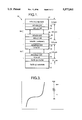
- FIG. 1 is a cross-sectional view, depicting one embodiment of the superlattice-clad laser diode of the present invention
- FIG. 2 is a cross-sectional view depicting a schematic layer sequence diagram of an n-type AlAs/Al x Ga 1-x Sb superlattice cladding layer used in the laser diode of FIG. 1;
- FIG. 3 on coordinates of current and voltage, is an I-V plot for a diode comprising InAs(Be) grown on an n-type AlAs(Si)/AlSb(und) superlattice.
- the laser of the present invention operates like any semiconductor laser diode.
- An active region is sandwiched between B-type and p-type cladding layers.
- the diode is forward biased and electrons are injected into the active region from the n-type cladding region, while holes are injected from the p-type cladding region. Since the active region has a smaller bandgap than the cladding regions, the electrons and holes are confined in the active region, and most of them recombine radiatively.
- the photons generated in the active region are optically guided, since the index of refraction is higher in the active region than in the cladding layers.
- the cladding layers confine the carriers as well as the light to thereby form a waveguide.
- the present invention is considered unique in that selectively-doped "superlattice” cladding layers are employed.
- the term “superlattice” refers to an alternating structure comprising a plurality of layers of two different semiconductor compounds, each layer being typically in the range of about 3 to 100 ⁇ .
- FIG. 1 depicts one example of the superlattice-clad laser diode of the present invention.
- an AlAs/AlGaSb superlattice laser structure 10 is formed on a p-doped GaSb substrate 12.
- a p + -doped GaSb buffer layer 14 is formed on the substrate 12, as is conventional in this art.
- a first superlattice clad layer 16 (p-type) comprises alternating layers of undoped AlAs 18 and p-doped AlGaSb 20 and is formed on the buffer layer 14.
- An active layer 22 comprising undoped InAsSb is formed on the first clad layer 16.
- a second superlattice clad layer 24 (n-type) comprises alternating layers of n-doped AlAs 26 and undoped AlGaSb 28 and is formed on the active layer 22.
- a cap layer comprising n + -doped InAs is formed on top of the second clad layer 24, completing the structure 10.
- the active region 22 may comprise conventional active region materials such as InAsSb or InGaAsSb.
- InAsSb given by the formula InAs z Sb 1-z wherein z is within the range of about 0.5 to 1, or InGaAsSb, given by the formula In w Ga 1-w As y Sb 1-y wherein w is within the range of about 0.09 to 1 and y is within the range of about 0.087 to 0.91, may be used.
- the buffer layer 14 is about 0.1 ⁇ m in thickness
- the first and second clad layers 16 and 24 are each about 3.0 ⁇ m in thickness, comprising AlAs layers 18 and 26 of 6 ⁇ and AlGaSb layers 20 and 28 of 60 ⁇ in thickness
- the active region 22 is about 0.2 ⁇ m in thickness
- the cap layer 30 is about 0.1 ⁇ m in thickness
- the alternating layers can comprise AlAs and Al x Ga 1-x Sb
- AlGaSb is given by the formula Al x Ga 1-x Sb where x is within the range of 0 to 1, or, preferably, is within the range of 0.4 to 1.
- the p-AlGaSb layers 20 are doped with beryllium, while the n-AlAs layers 26 are doped with silicon.
- FIG. 2 A schematic layer sequence diagram of the n-type AlAs/Al x Ga 1-x Sb superlattice cladding layer 24 is depicted in FIG. 2.
- the AlAs layers 26 are doped with silicon to a value of about 5 ⁇ 10 18 cm -3 to make them n-type.
- the Al x Ga 1-x Sb layers 28 are left undoped.
- the thickness of the AlAs(Si) layers 26 is, for example, about 2 monolayers, while the thickness of the AlGaSb(und) layers 28 is about 20 monolayers. As used herein, the term "(und)" indicates undoped.
- the superlattice clad structure 16, 24 starts with AlAs or with AlGaSb on the buffer layer 14 or the active layer 22.
- AlGaSb is used as the top layer of each cladding layer 16, 24.
- the thickness of the AlAs layers 18, 26 ranges from about 3 to 9 ⁇ (1 to 3 monolayers), and preferably is about 3 ⁇ .
- the thickness of the AlGaSb layers 20, 28 ranges from about 20 to 60 ⁇ , and preferably is about 30 ⁇ . Most preferably, the ratio of thickness of the two layers, AlAs:AlGaSb is 1:10.
- the substrate 12 material of choice for this combination is either GaSb or InAs. InAs as the substrate material is preferred, since it is easier for lattice-matching the AlAs/AlGaSb layers as compared to GaSb.
- AlAs(Si)/AlGaSb superlattices matched to GaSb with n-type carrier concentrations in excess of 1 ⁇ 10 18 cm -3 have been grown. Further, diode lasers employing this superlattice structure have been fabricated. However, lasing has not yet been observed, which is believed to be due to excessive lattice mismatch resulting from the difficulty of precisely controlling the amount of cross-incorporation of As in the AlGaSb. It is expected that further refinements of the growth of the superlattices will result in lasing of these structures.
- AlGaSb may be used as the alternating layer.
- x is preferably 1, so that the alternating set of layers is InAs/AlSb.
- the bandgap for the InAs/AlSb structure is not as large as that of the AlAs/AlGaSb superlattice cladding structure, and thus carrier confinement is not as good, nevertheless, it is not necessary to grow such thin As-containing layers. Rather, both layers may be approximately the same thickness, say 24 ⁇ (8 monolayers each).
- n-InAs is doped with silicon.
- p-AlGaSb is doped with beryllium, as above.
- the thickness of both InAs and AlGaSb ranges from about 3 to 50 ⁇ , and preferably from about 19 to 25 ⁇ . Most preferably, the ratio of thickness of the two layers is 1:1.
- the substrate 12 material of choice for this combination is GaSb.
- the InAs/AlGaSb structure is easier to grow by MBE than the AlAs/AlGaSb structure, due to the relaxing of thickness constraints. Indeed, several diode lasers were built with the InAs/AlGaSb cladding structure, and lasing was observed in the range of 2.24 to 3.90 ⁇ m.
- AlAs(Si)/AlGaSb(und) superlattices have been studied as laser cladding layers because they should provide excellent optical and carder confinement.
- the superlattice clads should provide excellent hole confinement in contrast to poor confinement of most mid-IR laser structures.
- Laser cladding layers must have a mobility which is sufficiently high to yield a low series resistance.
- electrons or holes are not expected to be trapped in the small band gap AlSb layers, measurement of vertical transport in diode structures incorporating these superlattices has been made.
- the current-voltage characteristics for p-InAs (n-AlAs/AlSb) diodes recently fabricated suggest that the electrons are mobile in the superlattice.
- the results also show that the superlattice can be made sufficiently n-type by doping the AlAs layers alone.
- the diodes comprise p-type InAs(Be) grown on an n-type AlAs(Si)/AlSb(und) superlattice. Be was used to dope the InAs and Si to dope the AlAs layers in the superlattice. These p-n junctions were grown on top of a 0.6 ⁇ m thick n-type InAs buffer layer separated from an n-type GaAs substrate by an n-InAs/GaAs short-period superlattice buffer layer.
- FIG. 3 shows an I-V curve for a 300 ⁇ m ⁇ 2 ⁇ m mesa.
- the 12 mA peak current corresponds to a current density of 2 kA/cm 2 , which should be more than adequate for a laser diode.
- the somewhat rounded knee in the low current pan of the curve is indicative of significant generation-recombination in the quasi-neutral region of the diode.
- the performance of the diodes depends on the manner in which the superlattices were doped. For some of the diodes, the Al half-monolayer at the interface between AlAs and AlSb was Si doped. These diodes out-performed those with no doping in these layers. In AlSb (or AlGaSb), Si would be expected to incorporate at the Sb sites as p-type dopant. However, the present inventors have found that Si is incorporated at Al sites (n-type dopant) when the Al is sandwiched between As and Sb layers.
- a double heterostructure has been grown with an InAs active layer sandwiched between n- and p-type AlAs/AlSb superlattice cladding layers.
- Optical (PL) and electrical characterization of this sample is in progress.
- the mid-IR lasers fabricated in accordance with the present invention can be used in hydrocarbon sensors, which have automotive and environmental applications. These sensors could be deployed in mines, tunnels, ship bilges, refineries, and the like. Use of the cladding superlattice of the invention avoids the necessity of using tellurium (or other Group VI) as a dopant.
Landscapes
- Physics & Mathematics (AREA)
- Condensed Matter Physics & Semiconductors (AREA)
- General Physics & Mathematics (AREA)
- Electromagnetism (AREA)
- Optics & Photonics (AREA)
- Geometry (AREA)
- Semiconductor Lasers (AREA)
Abstract
Description
Claims (18)
Priority Applications (1)
| Application Number | Priority Date | Filing Date | Title |
|---|---|---|---|
| US08/359,751 US5577061A (en) | 1994-12-16 | 1994-12-16 | Superlattice cladding layers for mid-infrared lasers |
Applications Claiming Priority (1)
| Application Number | Priority Date | Filing Date | Title |
|---|---|---|---|
| US08/359,751 US5577061A (en) | 1994-12-16 | 1994-12-16 | Superlattice cladding layers for mid-infrared lasers |
Publications (1)
| Publication Number | Publication Date |
|---|---|
| US5577061A true US5577061A (en) | 1996-11-19 |
Family
ID=23415127
Family Applications (1)
| Application Number | Title | Priority Date | Filing Date |
|---|---|---|---|
| US08/359,751 Expired - Lifetime US5577061A (en) | 1994-12-16 | 1994-12-16 | Superlattice cladding layers for mid-infrared lasers |
Country Status (1)
| Country | Link |
|---|---|
| US (1) | US5577061A (en) |
Cited By (60)
| Publication number | Priority date | Publication date | Assignee | Title |
|---|---|---|---|---|
| US5802090A (en) * | 1995-10-19 | 1998-09-01 | David Sarnoff Research Center, Inc. | Room temperature diode laser emitting in the 2-5 micrometer wavelength range |
| WO1998056091A1 (en) * | 1997-06-06 | 1998-12-10 | Northwestern University | LONG WAVELENGTH DH, SCH AND MQW LASERS BASED ON Sb |
| FR2775388A1 (en) * | 1998-02-26 | 1999-08-27 | Sagem | INDIUM-BASED ALLOY AND INFRARED TRANSDUCER USING SUCH ALLOY |
| US6320212B1 (en) | 1999-09-02 | 2001-11-20 | Hrl Laboratories, Llc. | Superlattice fabrication for InAs/GaSb/AISb semiconductor structures |
| US20040013155A1 (en) * | 2002-07-16 | 2004-01-22 | Dariusz Burak | Material systems for long wavelength lasers grown on GaSb or InAs substrates |
| WO2004059038A1 (en) * | 2002-12-27 | 2004-07-15 | Leiv Eiriksson Nyskaping As | Etching of algainassb |
| US20040223529A1 (en) * | 2003-05-08 | 2004-11-11 | Maxion Technologies, Inc. | Semiconductor laser cladding layers |
| US20050087738A1 (en) * | 2003-06-26 | 2005-04-28 | R.J. Mears Llc | Method for making a semiconductor device including band-engineered superlattice having 3/1-5/1 germanium layer structure |
| US20050167653A1 (en) * | 2003-06-26 | 2005-08-04 | Rj Mears, Llc | Semiconductor device including a superlattice with regions defining a semiconductor junction |
| US20050170590A1 (en) * | 2003-06-26 | 2005-08-04 | Rj Mears, Llc. | Method for making a semiconductor device including a superlattice with regions defining a semiconductor junction |
| US20050167649A1 (en) * | 2003-06-26 | 2005-08-04 | Rj Mears, Llc | Semiconductor device including a superlattice and adjacent semiconductor layer with doped regions defining a semiconductor junction |
| US20050170591A1 (en) * | 2003-06-26 | 2005-08-04 | Rj Mears, Llc | Method for making a semiconductor device including a superlattice and adjacent semiconductor layer with doped regions defining a semiconductor junction |
| US20050282330A1 (en) * | 2003-06-26 | 2005-12-22 | Rj Mears, Llc | Method for making a semiconductor device including a superlattice having at least one group of substantially undoped layers |
| US20050279991A1 (en) * | 2003-06-26 | 2005-12-22 | Rj Mears, Llc | Semiconductor device including a superlattice having at least one group of substantially undoped layers |
| DE102004023977A1 (en) * | 2004-05-14 | 2006-01-19 | Fraunhofer-Gesellschaft zur Förderung der angewandten Forschung e.V. | Transparent contact and process for its production |
| US20060011905A1 (en) * | 2003-06-26 | 2006-01-19 | Rj Mears, Llc | Semiconductor device comprising a superlattice dielectric interface layer |
| US20060019454A1 (en) * | 2003-06-26 | 2006-01-26 | Rj Mears, Llc | Method for making a semiconductor device comprising a superlattice dielectric interface layer |
| US20060202189A1 (en) * | 2003-06-26 | 2006-09-14 | Rj Mears, Llc | Semiconductor device including a memory cell with a negative differential resistance (ndr) device |
| US20060220118A1 (en) * | 2003-06-26 | 2006-10-05 | Rj Mears, Llc | Semiconductor device including a dopant blocking superlattice |
| US20060226502A1 (en) * | 2003-06-26 | 2006-10-12 | Rj Mears, Llc | Microelectromechanical Systems (MEMS) Device Including a Superlattice |
| US20060231857A1 (en) * | 2003-06-26 | 2006-10-19 | Rj Mears, Llc | Method for making a semiconductor device including a memory cell with a negative differential resistance (ndr) device |
| US20060243964A1 (en) * | 2003-06-26 | 2006-11-02 | Rj Mears, Llc | Method for making a semiconductor device having a semiconductor-on-insulator configuration and a superlattice |
| US20060261327A1 (en) * | 2003-06-26 | 2006-11-23 | Rj Mears, Llc | Semiconductor device having a semiconductor-on-insulator configuration and a superlattice |
| US20060267130A1 (en) * | 2003-06-26 | 2006-11-30 | Rj Mears, Llc | Semiconductor Device Including Shallow Trench Isolation (STI) Regions with a Superlattice Therebetween |
| US20060270169A1 (en) * | 2003-06-26 | 2006-11-30 | Rj Mears, Llc | Method for Making a Semiconductor Device Including Shallow Trench Isolation (STI) Regions with a Superlattice Therebetween |
| US20060273299A1 (en) * | 2003-06-26 | 2006-12-07 | Rj Mears, Llc | Method for making a semiconductor device including a dopant blocking superlattice |
| US7153763B2 (en) | 2003-06-26 | 2006-12-26 | Rj Mears, Llc | Method for making a semiconductor device including band-engineered superlattice using intermediate annealing |
| US20060292818A1 (en) * | 2003-06-26 | 2006-12-28 | Rj Mears, Llc | Method for Making a Semiconductor Device Having a Semiconductor-on-Insulator (SOI) Configuration and Including a Superlattice on a Thin Semiconductor Layer |
| US20060292765A1 (en) * | 2003-06-26 | 2006-12-28 | Rj Mears, Llc | Method for Making a FINFET Including a Superlattice |
| US20060289049A1 (en) * | 2003-06-26 | 2006-12-28 | Rj Mears, Llc | Semiconductor Device Having a Semiconductor-on-Insulator (SOI) Configuration and Including a Superlattice on a Thin Semiconductor Layer |
| US20060292889A1 (en) * | 2003-06-26 | 2006-12-28 | Rj Mears, Llc | FINFET Including a Superlattice |
| US20070010040A1 (en) * | 2003-06-26 | 2007-01-11 | Rj Mears, Llc | Method for Making a Semiconductor Device Including a Strained Superlattice Layer Above a Stress Layer |
| US20070007508A1 (en) * | 2003-06-26 | 2007-01-11 | Rj Mears, Llc | Semiconductor Device Including a Strained Superlattice Layer Above a Stress Layer |
| US20070012909A1 (en) * | 2003-06-26 | 2007-01-18 | Rj Mears, Llc | Semiconductor Device Including a Strained Superlattice Between at Least One Pair of Spaced Apart Stress Regions |
| US20070012912A1 (en) * | 2003-06-26 | 2007-01-18 | Rj Mears, Llc | Semiconductor Device Including a Strained Superlattice and Overlying Stress Layer and Related Methods |
| US20070012999A1 (en) * | 2003-06-26 | 2007-01-18 | Rj Mears, Llc | Method for Making a Semiconductor Device Including Regions of Band-Engineered Semiconductor Superlattice to Reduce Device-On Resistance |
| US20070012911A1 (en) * | 2003-06-26 | 2007-01-18 | Rj Mears, Llc | Semiconductor Device Including Regions of Band-Engineered Semiconductor Superlattice to Reduce Device-On Resistance |
| US20070015344A1 (en) * | 2003-06-26 | 2007-01-18 | Rj Mears, Llc | Method for Making a Semiconductor Device Including a Strained Superlattice Between at Least One Pair of Spaced Apart Stress Regions |
| US20070020833A1 (en) * | 2003-06-26 | 2007-01-25 | Rj Mears, Llc | Method for Making a Semiconductor Device Including a Channel with a Non-Semiconductor Layer Monolayer |
| US20070020860A1 (en) * | 2003-06-26 | 2007-01-25 | Rj Mears, Llc | Method for Making Semiconductor Device Including a Strained Superlattice and Overlying Stress Layer and Related Methods |
| US20070063185A1 (en) * | 2003-06-26 | 2007-03-22 | Rj Mears, Llc | Semiconductor device including a front side strained superlattice layer and a back side stress layer |
| US20070063186A1 (en) * | 2003-06-26 | 2007-03-22 | Rj Mears, Llc | Method for making a semiconductor device including a front side strained superlattice layer and a back side stress layer |
| US20070158640A1 (en) * | 2005-12-22 | 2007-07-12 | Rj Mears, Llc | Electronic device including a poled superlattice having a net electrical dipole moment |
| US20070161138A1 (en) * | 2005-12-22 | 2007-07-12 | Rj Mears, Llc | Method for making an electronic device including a poled superlattice having a net electrical dipole moment |
| US20070194298A1 (en) * | 2006-02-21 | 2007-08-23 | Rj Mears, Llc | Semiconductor device comprising a lattice matching layer |
| US20080179588A1 (en) * | 2007-01-25 | 2008-07-31 | Mears Technologies, Inc. | Semiconductor device including a metal-to-semiconductor superlattice interface layer and related methods |
| US20080197340A1 (en) * | 2007-02-16 | 2008-08-21 | Rj Mears, Llc | Multiple-wavelength opto-electronic device including a superlattice |
| US20080197341A1 (en) * | 2007-02-16 | 2008-08-21 | Rj Mears, Llc | Method for making a multiple-wavelength opto-electronic device including a superlattice |
| US20080258134A1 (en) * | 2007-04-23 | 2008-10-23 | Mears Technologies, Inc. | Method for making a semiconductor device including shallow trench isolation (sti) regions with maskless superlattice deposition following sti formation and related structures |
| US7659539B2 (en) | 2003-06-26 | 2010-02-09 | Mears Technologies, Inc. | Semiconductor device including a floating gate memory cell with a superlattice channel |
| US7781827B2 (en) | 2007-01-24 | 2010-08-24 | Mears Technologies, Inc. | Semiconductor device with a vertical MOSFET including a superlattice and related methods |
| US9012851B2 (en) | 2010-10-14 | 2015-04-21 | Thermo Fisher Scientific (Bremen) Gmbh | Optical chamber module assembly |
| US9275996B2 (en) | 2013-11-22 | 2016-03-01 | Mears Technologies, Inc. | Vertical semiconductor devices including superlattice punch through stop layer and related methods |
| US9406753B2 (en) | 2013-11-22 | 2016-08-02 | Atomera Incorporated | Semiconductor devices including superlattice depletion layer stack and related methods |
| US9558939B1 (en) | 2016-01-15 | 2017-01-31 | Atomera Incorporated | Methods for making a semiconductor device including atomic layer structures using N2O as an oxygen source |
| US9651488B2 (en) | 2010-10-14 | 2017-05-16 | Thermo Fisher Scientific (Bremen) Gmbh | High-accuracy mid-IR laser-based gas sensor |
| US9716147B2 (en) | 2014-06-09 | 2017-07-25 | Atomera Incorporated | Semiconductor devices with enhanced deterministic doping and related methods |
| US9721790B2 (en) | 2015-06-02 | 2017-08-01 | Atomera Incorporated | Method for making enhanced semiconductor structures in single wafer processing chamber with desired uniformity control |
| US9722046B2 (en) | 2014-11-25 | 2017-08-01 | Atomera Incorporated | Semiconductor device including a superlattice and replacement metal gate structure and related methods |
| US9899479B2 (en) | 2015-05-15 | 2018-02-20 | Atomera Incorporated | Semiconductor devices with superlattice layers providing halo implant peak confinement and related methods |
Citations (8)
| Publication number | Priority date | Publication date | Assignee | Title |
|---|---|---|---|---|
| JPS60130878A (en) * | 1983-12-19 | 1985-07-12 | Nec Corp | Superlattice semiconductor laser |
| JPS61154191A (en) * | 1984-12-27 | 1986-07-12 | Mitsubishi Electric Corp | Semiconductor laser element |
| JPS61181185A (en) * | 1985-02-07 | 1986-08-13 | Nec Corp | Semiconductor light-emitting element |
| JPS6251282A (en) * | 1985-08-30 | 1987-03-05 | Sony Corp | Semiconductor laser |
| JPS63245984A (en) * | 1987-04-01 | 1988-10-13 | Seiko Epson Corp | Semiconductor light emitting element and manufacture thereof |
| US4882734A (en) * | 1988-03-09 | 1989-11-21 | Xerox Corporation | Quantum well heterostructure lasers with low current density threshold and higher TO values |
| US5007063A (en) * | 1990-02-12 | 1991-04-09 | Eastman Kodak Company | Laser diode |
| US5251225A (en) * | 1992-05-08 | 1993-10-05 | Massachusetts Institute Of Technology | Quantum-well diode laser |
-
1994
- 1994-12-16 US US08/359,751 patent/US5577061A/en not_active Expired - Lifetime
Patent Citations (8)
| Publication number | Priority date | Publication date | Assignee | Title |
|---|---|---|---|---|
| JPS60130878A (en) * | 1983-12-19 | 1985-07-12 | Nec Corp | Superlattice semiconductor laser |
| JPS61154191A (en) * | 1984-12-27 | 1986-07-12 | Mitsubishi Electric Corp | Semiconductor laser element |
| JPS61181185A (en) * | 1985-02-07 | 1986-08-13 | Nec Corp | Semiconductor light-emitting element |
| JPS6251282A (en) * | 1985-08-30 | 1987-03-05 | Sony Corp | Semiconductor laser |
| JPS63245984A (en) * | 1987-04-01 | 1988-10-13 | Seiko Epson Corp | Semiconductor light emitting element and manufacture thereof |
| US4882734A (en) * | 1988-03-09 | 1989-11-21 | Xerox Corporation | Quantum well heterostructure lasers with low current density threshold and higher TO values |
| US5007063A (en) * | 1990-02-12 | 1991-04-09 | Eastman Kodak Company | Laser diode |
| US5251225A (en) * | 1992-05-08 | 1993-10-05 | Massachusetts Institute Of Technology | Quantum-well diode laser |
Non-Patent Citations (8)
| Title |
|---|
| "High-power multiple-quantum-well GalnAsSb/A1GaAsSb diode lasers emitting at 2.1 μm with low threshold current density", H. K. Choi et al, Applied Physics Letters, vol. 61(10), pp. 1154-1156 (7 Sep. 1992). |
| "InAsSb/A1AsSb double-heterostructure diode lasers emitting at 4 μm", S. J. Eglash et al, Applied Physics Letters, vol. 64(7), pp. 883-835 (14 Feb. 1994). |
| Choi, H. K., Eglash, S., "High-Efficiency High-Power GaLnAsSb--ALGaAsSb Double-Heterostructure Lasers Emitting a t 2.3 microns", IEEE Journal of Quantum Electronics, vol 27, No. 6, Jun. 1991 pp. 1555-1559. |
| Choi, H. K., Eglash, S., High Efficiency High Power GaLnAsSb ALGaAsSb Double Heterostructure Lasers Emitting a t 2.3 microns , IEEE Journal of Quantum Electronics, vol 27, No. 6, Jun. 1991 pp. 1555 1559. * |
| High power multiple quantum well GalnAsSb/A1GaAsSb diode lasers emitting at 2.1 m with low threshold current density , H. K. Choi et al, Applied Physics Letters, vol. 61(10), pp. 1154 1156 (7 Sep. 1992). * |
| InAsSb/A1AsSb double heterostructure diode lasers emitting at 4 m , S. J. Eglash et al, Applied Physics Letters, vol. 64(7), pp. 883 835 (14 Feb. 1994). * |
| Shen et al, Remote n type modulation doping of InAs quantum wells by deep acceptors in ALSb ,Journal of Applied Physics. 73(12),June 15 1993,pp. 8313 8318. * |
| Shen et al,"Remote n-type modulation doping of InAs quantum wells by `deep acceptors`in ALSb",Journal of Applied Physics. 73(12),June 15 1993,pp. 8313-8318. |
Cited By (103)
| Publication number | Priority date | Publication date | Assignee | Title |
|---|---|---|---|---|
| US5802090A (en) * | 1995-10-19 | 1998-09-01 | David Sarnoff Research Center, Inc. | Room temperature diode laser emitting in the 2-5 micrometer wavelength range |
| WO1998056091A1 (en) * | 1997-06-06 | 1998-12-10 | Northwestern University | LONG WAVELENGTH DH, SCH AND MQW LASERS BASED ON Sb |
| US6108360A (en) * | 1997-06-06 | 2000-08-22 | Razeghi; Manijeh | Long wavelength DH, SCH and MQW lasers based on Sb |
| FR2775388A1 (en) * | 1998-02-26 | 1999-08-27 | Sagem | INDIUM-BASED ALLOY AND INFRARED TRANSDUCER USING SUCH ALLOY |
| EP0939447A1 (en) * | 1998-02-26 | 1999-09-01 | Sagem Sa | Indium based alloy and infrared transducer using the same |
| US6274882B1 (en) | 1998-02-26 | 2001-08-14 | Sagem Sa | Indium-based alloy and an infrared transducer using such an alloy |
| US6320212B1 (en) | 1999-09-02 | 2001-11-20 | Hrl Laboratories, Llc. | Superlattice fabrication for InAs/GaSb/AISb semiconductor structures |
| US6727153B2 (en) | 1999-09-02 | 2004-04-27 | Hrl Laboratories, Llc | Superlattice fabrication for InAs/GaSb/AlSb semiconductor structures |
| US20040013155A1 (en) * | 2002-07-16 | 2004-01-22 | Dariusz Burak | Material systems for long wavelength lasers grown on GaSb or InAs substrates |
| US6813297B2 (en) * | 2002-07-16 | 2004-11-02 | Agilent Technologies, Inc. | Material systems for long wavelength lasers grown on GaSb or InAs substrates |
| WO2004059038A1 (en) * | 2002-12-27 | 2004-07-15 | Leiv Eiriksson Nyskaping As | Etching of algainassb |
| US20110021032A1 (en) * | 2002-12-27 | 2011-01-27 | Renato Bugge | Etching of AlGaInAsSb |
| US20040223529A1 (en) * | 2003-05-08 | 2004-11-11 | Maxion Technologies, Inc. | Semiconductor laser cladding layers |
| US20070063186A1 (en) * | 2003-06-26 | 2007-03-22 | Rj Mears, Llc | Method for making a semiconductor device including a front side strained superlattice layer and a back side stress layer |
| US20070010040A1 (en) * | 2003-06-26 | 2007-01-11 | Rj Mears, Llc | Method for Making a Semiconductor Device Including a Strained Superlattice Layer Above a Stress Layer |
| US20050170590A1 (en) * | 2003-06-26 | 2005-08-04 | Rj Mears, Llc. | Method for making a semiconductor device including a superlattice with regions defining a semiconductor junction |
| US20050167649A1 (en) * | 2003-06-26 | 2005-08-04 | Rj Mears, Llc | Semiconductor device including a superlattice and adjacent semiconductor layer with doped regions defining a semiconductor junction |
| US20050170591A1 (en) * | 2003-06-26 | 2005-08-04 | Rj Mears, Llc | Method for making a semiconductor device including a superlattice and adjacent semiconductor layer with doped regions defining a semiconductor junction |
| US20050282330A1 (en) * | 2003-06-26 | 2005-12-22 | Rj Mears, Llc | Method for making a semiconductor device including a superlattice having at least one group of substantially undoped layers |
| US20050279991A1 (en) * | 2003-06-26 | 2005-12-22 | Rj Mears, Llc | Semiconductor device including a superlattice having at least one group of substantially undoped layers |
| US20060011905A1 (en) * | 2003-06-26 | 2006-01-19 | Rj Mears, Llc | Semiconductor device comprising a superlattice dielectric interface layer |
| US20060019454A1 (en) * | 2003-06-26 | 2006-01-26 | Rj Mears, Llc | Method for making a semiconductor device comprising a superlattice dielectric interface layer |
| US7034329B2 (en) | 2003-06-26 | 2006-04-25 | Rj Mears, Llc | Semiconductor device including band-engineered superlattice having 3/1-5/1 germanium layer structure |
| US7045813B2 (en) | 2003-06-26 | 2006-05-16 | Rj Mears, Llc | Semiconductor device including a superlattice with regions defining a semiconductor junction |
| US7045377B2 (en) | 2003-06-26 | 2006-05-16 | Rj Mears, Llc | Method for making a semiconductor device including a superlattice and adjacent semiconductor layer with doped regions defining a semiconductor junction |
| US7071119B2 (en) | 2003-06-26 | 2006-07-04 | Rj Mears, Llc | Method for making a semiconductor device including band-engineered superlattice having 3/1-5/1 germanium layer structure |
| US20060202189A1 (en) * | 2003-06-26 | 2006-09-14 | Rj Mears, Llc | Semiconductor device including a memory cell with a negative differential resistance (ndr) device |
| US20060220118A1 (en) * | 2003-06-26 | 2006-10-05 | Rj Mears, Llc | Semiconductor device including a dopant blocking superlattice |
| US20060226502A1 (en) * | 2003-06-26 | 2006-10-12 | Rj Mears, Llc | Microelectromechanical Systems (MEMS) Device Including a Superlattice |
| US20060231857A1 (en) * | 2003-06-26 | 2006-10-19 | Rj Mears, Llc | Method for making a semiconductor device including a memory cell with a negative differential resistance (ndr) device |
| US20060243964A1 (en) * | 2003-06-26 | 2006-11-02 | Rj Mears, Llc | Method for making a semiconductor device having a semiconductor-on-insulator configuration and a superlattice |
| US20060261327A1 (en) * | 2003-06-26 | 2006-11-23 | Rj Mears, Llc | Semiconductor device having a semiconductor-on-insulator configuration and a superlattice |
| US20060267130A1 (en) * | 2003-06-26 | 2006-11-30 | Rj Mears, Llc | Semiconductor Device Including Shallow Trench Isolation (STI) Regions with a Superlattice Therebetween |
| US20060270169A1 (en) * | 2003-06-26 | 2006-11-30 | Rj Mears, Llc | Method for Making a Semiconductor Device Including Shallow Trench Isolation (STI) Regions with a Superlattice Therebetween |
| US20060273299A1 (en) * | 2003-06-26 | 2006-12-07 | Rj Mears, Llc | Method for making a semiconductor device including a dopant blocking superlattice |
| US7153763B2 (en) | 2003-06-26 | 2006-12-26 | Rj Mears, Llc | Method for making a semiconductor device including band-engineered superlattice using intermediate annealing |
| US20060292818A1 (en) * | 2003-06-26 | 2006-12-28 | Rj Mears, Llc | Method for Making a Semiconductor Device Having a Semiconductor-on-Insulator (SOI) Configuration and Including a Superlattice on a Thin Semiconductor Layer |
| US20060292765A1 (en) * | 2003-06-26 | 2006-12-28 | Rj Mears, Llc | Method for Making a FINFET Including a Superlattice |
| US20060289049A1 (en) * | 2003-06-26 | 2006-12-28 | Rj Mears, Llc | Semiconductor Device Having a Semiconductor-on-Insulator (SOI) Configuration and Including a Superlattice on a Thin Semiconductor Layer |
| US20060292889A1 (en) * | 2003-06-26 | 2006-12-28 | Rj Mears, Llc | FINFET Including a Superlattice |
| US7531828B2 (en) | 2003-06-26 | 2009-05-12 | Mears Technologies, Inc. | Semiconductor device including a strained superlattice between at least one pair of spaced apart stress regions |
| US20070007508A1 (en) * | 2003-06-26 | 2007-01-11 | Rj Mears, Llc | Semiconductor Device Including a Strained Superlattice Layer Above a Stress Layer |
| US20070012909A1 (en) * | 2003-06-26 | 2007-01-18 | Rj Mears, Llc | Semiconductor Device Including a Strained Superlattice Between at Least One Pair of Spaced Apart Stress Regions |
| US20070012912A1 (en) * | 2003-06-26 | 2007-01-18 | Rj Mears, Llc | Semiconductor Device Including a Strained Superlattice and Overlying Stress Layer and Related Methods |
| US20070012999A1 (en) * | 2003-06-26 | 2007-01-18 | Rj Mears, Llc | Method for Making a Semiconductor Device Including Regions of Band-Engineered Semiconductor Superlattice to Reduce Device-On Resistance |
| US20070012911A1 (en) * | 2003-06-26 | 2007-01-18 | Rj Mears, Llc | Semiconductor Device Including Regions of Band-Engineered Semiconductor Superlattice to Reduce Device-On Resistance |
| US20070015344A1 (en) * | 2003-06-26 | 2007-01-18 | Rj Mears, Llc | Method for Making a Semiconductor Device Including a Strained Superlattice Between at Least One Pair of Spaced Apart Stress Regions |
| US20070020833A1 (en) * | 2003-06-26 | 2007-01-25 | Rj Mears, Llc | Method for Making a Semiconductor Device Including a Channel with a Non-Semiconductor Layer Monolayer |
| US20070020860A1 (en) * | 2003-06-26 | 2007-01-25 | Rj Mears, Llc | Method for Making Semiconductor Device Including a Strained Superlattice and Overlying Stress Layer and Related Methods |
| US20070063185A1 (en) * | 2003-06-26 | 2007-03-22 | Rj Mears, Llc | Semiconductor device including a front side strained superlattice layer and a back side stress layer |
| US20050087736A1 (en) * | 2003-06-26 | 2005-04-28 | Rj Mears, Llc. | Semiconductor device including band-engineered superlattice having 3/1-5/1 germanium layer structure |
| US7202494B2 (en) | 2003-06-26 | 2007-04-10 | Rj Mears, Llc | FINFET including a superlattice |
| US7227174B2 (en) | 2003-06-26 | 2007-06-05 | Rj Mears, Llc | Semiconductor device including a superlattice and adjacent semiconductor layer with doped regions defining a semiconductor junction |
| US7229902B2 (en) | 2003-06-26 | 2007-06-12 | Rj Mears, Llc | Method for making a semiconductor device including a superlattice with regions defining a semiconductor junction |
| US7446002B2 (en) | 2003-06-26 | 2008-11-04 | Mears Technologies, Inc. | Method for making a semiconductor device comprising a superlattice dielectric interface layer |
| US7531829B2 (en) | 2003-06-26 | 2009-05-12 | Mears Technologies, Inc. | Semiconductor device including regions of band-engineered semiconductor superlattice to reduce device-on resistance |
| US20050087738A1 (en) * | 2003-06-26 | 2005-04-28 | R.J. Mears Llc | Method for making a semiconductor device including band-engineered superlattice having 3/1-5/1 germanium layer structure |
| US7659539B2 (en) | 2003-06-26 | 2010-02-09 | Mears Technologies, Inc. | Semiconductor device including a floating gate memory cell with a superlattice channel |
| US20050167653A1 (en) * | 2003-06-26 | 2005-08-04 | Rj Mears, Llc | Semiconductor device including a superlattice with regions defining a semiconductor junction |
| US7612366B2 (en) | 2003-06-26 | 2009-11-03 | Mears Technologies, Inc. | Semiconductor device including a strained superlattice layer above a stress layer |
| US7598515B2 (en) | 2003-06-26 | 2009-10-06 | Mears Technologies, Inc. | Semiconductor device including a strained superlattice and overlying stress layer and related methods |
| US7586165B2 (en) | 2003-06-26 | 2009-09-08 | Mears Technologies, Inc. | Microelectromechanical systems (MEMS) device including a superlattice |
| US7586116B2 (en) | 2003-06-26 | 2009-09-08 | Mears Technologies, Inc. | Semiconductor device having a semiconductor-on-insulator configuration and a superlattice |
| US7535041B2 (en) | 2003-06-26 | 2009-05-19 | Mears Technologies, Inc. | Method for making a semiconductor device including regions of band-engineered semiconductor superlattice to reduce device-on resistance |
| US7531850B2 (en) | 2003-06-26 | 2009-05-12 | Mears Technologies, Inc. | Semiconductor device including a memory cell with a negative differential resistance (NDR) device |
| US7491587B2 (en) | 2003-06-26 | 2009-02-17 | Mears Technologies, Inc. | Method for making a semiconductor device having a semiconductor-on-insulator (SOI) configuration and including a superlattice on a thin semiconductor layer |
| US7514328B2 (en) | 2003-06-26 | 2009-04-07 | Mears Technologies, Inc. | Method for making a semiconductor device including shallow trench isolation (STI) regions with a superlattice therebetween |
| DE102004023977A1 (en) * | 2004-05-14 | 2006-01-19 | Fraunhofer-Gesellschaft zur Förderung der angewandten Forschung e.V. | Transparent contact and process for its production |
| US20070166928A1 (en) * | 2005-12-22 | 2007-07-19 | Rj Mears, Llc | Method for making an electronic device including a selectively polable superlattice |
| US7517702B2 (en) | 2005-12-22 | 2009-04-14 | Mears Technologies, Inc. | Method for making an electronic device including a poled superlattice having a net electrical dipole moment |
| US20070158640A1 (en) * | 2005-12-22 | 2007-07-12 | Rj Mears, Llc | Electronic device including a poled superlattice having a net electrical dipole moment |
| US20070187667A1 (en) * | 2005-12-22 | 2007-08-16 | Rj Mears, Llc | Electronic device including a selectively polable superlattice |
| US20070161138A1 (en) * | 2005-12-22 | 2007-07-12 | Rj Mears, Llc | Method for making an electronic device including a poled superlattice having a net electrical dipole moment |
| US7718996B2 (en) | 2006-02-21 | 2010-05-18 | Mears Technologies, Inc. | Semiconductor device comprising a lattice matching layer |
| US20070197006A1 (en) * | 2006-02-21 | 2007-08-23 | Rj Mears, Llc | Method for making a semiconductor device comprising a lattice matching layer |
| US20070194298A1 (en) * | 2006-02-21 | 2007-08-23 | Rj Mears, Llc | Semiconductor device comprising a lattice matching layer |
| US7700447B2 (en) | 2006-02-21 | 2010-04-20 | Mears Technologies, Inc. | Method for making a semiconductor device comprising a lattice matching layer |
| US7781827B2 (en) | 2007-01-24 | 2010-08-24 | Mears Technologies, Inc. | Semiconductor device with a vertical MOSFET including a superlattice and related methods |
| US7928425B2 (en) | 2007-01-25 | 2011-04-19 | Mears Technologies, Inc. | Semiconductor device including a metal-to-semiconductor superlattice interface layer and related methods |
| US20080179588A1 (en) * | 2007-01-25 | 2008-07-31 | Mears Technologies, Inc. | Semiconductor device including a metal-to-semiconductor superlattice interface layer and related methods |
| US7863066B2 (en) | 2007-02-16 | 2011-01-04 | Mears Technologies, Inc. | Method for making a multiple-wavelength opto-electronic device including a superlattice |
| US20080197340A1 (en) * | 2007-02-16 | 2008-08-21 | Rj Mears, Llc | Multiple-wavelength opto-electronic device including a superlattice |
| US7880161B2 (en) | 2007-02-16 | 2011-02-01 | Mears Technologies, Inc. | Multiple-wavelength opto-electronic device including a superlattice |
| US20080197341A1 (en) * | 2007-02-16 | 2008-08-21 | Rj Mears, Llc | Method for making a multiple-wavelength opto-electronic device including a superlattice |
| US8389974B2 (en) | 2007-02-16 | 2013-03-05 | Mears Technologies, Inc. | Multiple-wavelength opto-electronic device including a superlattice |
| US20080258134A1 (en) * | 2007-04-23 | 2008-10-23 | Mears Technologies, Inc. | Method for making a semiconductor device including shallow trench isolation (sti) regions with maskless superlattice deposition following sti formation and related structures |
| US7812339B2 (en) | 2007-04-23 | 2010-10-12 | Mears Technologies, Inc. | Method for making a semiconductor device including shallow trench isolation (STI) regions with maskless superlattice deposition following STI formation and related structures |
| US9651488B2 (en) | 2010-10-14 | 2017-05-16 | Thermo Fisher Scientific (Bremen) Gmbh | High-accuracy mid-IR laser-based gas sensor |
| US9012851B2 (en) | 2010-10-14 | 2015-04-21 | Thermo Fisher Scientific (Bremen) Gmbh | Optical chamber module assembly |
| US10295464B2 (en) | 2011-09-09 | 2019-05-21 | Thermo Fisher Scientific (Bremen) Gmbh | High-accuracy mid-IR laser-based gas sensor |
| US20170248517A1 (en) * | 2011-09-09 | 2017-08-31 | Thermo Fisher Scientific (Bremen) Gmbh | High-accuracy mid-ir laseer-based gas sensor |
| US10107751B2 (en) * | 2011-09-09 | 2018-10-23 | Thermo Fisher Scientific (Bremen) Gmbh | High-accuracy mid-IR laser-based gas sensor |
| US9972685B2 (en) | 2013-11-22 | 2018-05-15 | Atomera Incorporated | Vertical semiconductor devices including superlattice punch through stop layer and related methods |
| US9406753B2 (en) | 2013-11-22 | 2016-08-02 | Atomera Incorporated | Semiconductor devices including superlattice depletion layer stack and related methods |
| US9275996B2 (en) | 2013-11-22 | 2016-03-01 | Mears Technologies, Inc. | Vertical semiconductor devices including superlattice punch through stop layer and related methods |
| US9716147B2 (en) | 2014-06-09 | 2017-07-25 | Atomera Incorporated | Semiconductor devices with enhanced deterministic doping and related methods |
| US10170560B2 (en) | 2014-06-09 | 2019-01-01 | Atomera Incorporated | Semiconductor devices with enhanced deterministic doping and related methods |
| US9722046B2 (en) | 2014-11-25 | 2017-08-01 | Atomera Incorporated | Semiconductor device including a superlattice and replacement metal gate structure and related methods |
| US10084045B2 (en) | 2014-11-25 | 2018-09-25 | Atomera Incorporated | Semiconductor device including a superlattice and replacement metal gate structure and related methods |
| US9941359B2 (en) | 2015-05-15 | 2018-04-10 | Atomera Incorporated | Semiconductor devices with superlattice and punch-through stop (PTS) layers at different depths and related methods |
| US9899479B2 (en) | 2015-05-15 | 2018-02-20 | Atomera Incorporated | Semiconductor devices with superlattice layers providing halo implant peak confinement and related methods |
| US9721790B2 (en) | 2015-06-02 | 2017-08-01 | Atomera Incorporated | Method for making enhanced semiconductor structures in single wafer processing chamber with desired uniformity control |
| US9558939B1 (en) | 2016-01-15 | 2017-01-31 | Atomera Incorporated | Methods for making a semiconductor device including atomic layer structures using N2O as an oxygen source |
Similar Documents
| Publication | Publication Date | Title |
|---|---|---|
| US5577061A (en) | Superlattice cladding layers for mid-infrared lasers | |
| US5181086A (en) | Strained superlattice semiconductor structure | |
| US5780867A (en) | Broadband light-emitting diode | |
| KR0153781B1 (en) | Elimination of heterojunction band discontinuities and its method | |
| US5548128A (en) | Direct-gap germanium-tin multiple-quantum-well electro-optical devices on silicon or germanium substrates | |
| US7732823B2 (en) | Light emitting device and semiconductor device | |
| US5594750A (en) | Selectively Si-doped InAs/A1AsSb short-period-superlattices as N-type cladding layers for mid-IR laser structures grown on InAs substrates | |
| US5726462A (en) | Semiconductor structures having electrically insulating and conducting portions formed from an AlSb-alloy layer | |
| JP2512422B2 (en) | Semiconductor device | |
| US6600169B2 (en) | Quantum dash device | |
| US5237581A (en) | Semiconductor multilayer reflector and light emitting device with the same | |
| Forouhar et al. | InGaAs/InGaAsP/InP strained-layer quantum well lasers at approximately 2 mu m | |
| KR0119796B1 (en) | Semiconductor laser | |
| US6711195B2 (en) | Long-wavelength photonic device with GaAsSb quantum-well layer | |
| EP0978912A2 (en) | Multi-quantum well lasers with selectively doped barriers | |
| US5436468A (en) | Ordered mixed crystal semiconductor superlattice device | |
| US5113231A (en) | Quantum-effect semiconductor devices | |
| US20060027823A1 (en) | Semiconductor conductive layers | |
| US9548414B2 (en) | Optical device based on bismuth-containing III-V compound multilayer semiconductors | |
| Tu | III-NV low-bandgap nitrides and their device applications | |
| KR100385039B1 (en) | Semiconductor device | |
| JPH01146390A (en) | Semiconductor device | |
| US5475700A (en) | Laser diode with electron and hole confinement and barrier layers | |
| KR920006434B1 (en) | Resonant tunelling barrier structure device | |
| US7986721B2 (en) | Semiconductor optical device including a PN junction formed by a second region of a first conductive type semiconductor layer and a second conductive type single semiconductor layer |
Legal Events
| Date | Code | Title | Description |
|---|---|---|---|
| AS | Assignment |
Owner name: HUGHES AIRCRAFT COMPANY, CALIFORNIA Free format text: ASSIGNMENT OF ASSIGNORS INTEREST;ASSIGNORS:HASENBERG, THOMAS C.;CHOW, DAVID H.;REEL/FRAME:007273/0908 Effective date: 19941212 |
|
| STCF | Information on status: patent grant |
Free format text: PATENTED CASE |
|
| AS | Assignment |
Owner name: AIR FORCE, UNITED STATES, VIRGINIA Free format text: CONFIRMATORY LICENSE;ASSIGNOR:HUGHES AIRCRAFT COMPANY;REEL/FRAME:008843/0346 Effective date: 19951017 |
|
| AS | Assignment |
Owner name: HUGHES ELECTRONICS CORPORATION, CALIFORNIA Free format text: ASSIGNMENT OF ASSIGNORS INTEREST;ASSIGNOR:HE HOLDINGS INC., HUGHES ELECTRONICS FORMERLY KNOWN AS HUGHES AIRCRAFT COMPANY;REEL/FRAME:009350/0366 Effective date: 19971217 |
|
| FPAY | Fee payment |
Year of fee payment: 4 |
|
| FEPP | Fee payment procedure |
Free format text: PAYOR NUMBER ASSIGNED (ORIGINAL EVENT CODE: ASPN); ENTITY STATUS OF PATENT OWNER: LARGE ENTITY Free format text: PAYER NUMBER DE-ASSIGNED (ORIGINAL EVENT CODE: RMPN); ENTITY STATUS OF PATENT OWNER: LARGE ENTITY |
|
| FPAY | Fee payment |
Year of fee payment: 8 |
|
| FPAY | Fee payment |
Year of fee payment: 12 |
|
| REMI | Maintenance fee reminder mailed |