EP1901597A1 - Plasma display module - Google Patents
Plasma display module Download PDFInfo
- Publication number
- EP1901597A1 EP1901597A1 EP07253649A EP07253649A EP1901597A1 EP 1901597 A1 EP1901597 A1 EP 1901597A1 EP 07253649 A EP07253649 A EP 07253649A EP 07253649 A EP07253649 A EP 07253649A EP 1901597 A1 EP1901597 A1 EP 1901597A1
- Authority
- EP
- European Patent Office
- Prior art keywords
- cover plate
- plasma display
- integrated circuit
- chassis
- display module
- Prior art date
- Legal status (The legal status is an assumption and is not a legal conclusion. Google has not performed a legal analysis and makes no representation as to the accuracy of the status listed.)
- Granted
Links
Images


Classifications
-
- H—ELECTRICITY
- H01—ELECTRIC ELEMENTS
- H01J—ELECTRIC DISCHARGE TUBES OR DISCHARGE LAMPS
- H01J11/00—Gas-filled discharge tubes with alternating current induction of the discharge, e.g. alternating current plasma display panels [AC-PDP]; Gas-filled discharge tubes without any main electrode inside the vessel; Gas-filled discharge tubes with at least one main electrode outside the vessel
- H01J11/20—Constructional details
- H01J11/34—Vessels, containers or parts thereof, e.g. substrates
-
- H—ELECTRICITY
- H05—ELECTRIC TECHNIQUES NOT OTHERWISE PROVIDED FOR
- H05K—PRINTED CIRCUITS; CASINGS OR CONSTRUCTIONAL DETAILS OF ELECTRIC APPARATUS; MANUFACTURE OF ASSEMBLAGES OF ELECTRICAL COMPONENTS
- H05K5/00—Casings, cabinets or drawers for electric apparatus
- H05K5/02—Details
- H05K5/0217—Mechanical details of casings
-
- H—ELECTRICITY
- H01—ELECTRIC ELEMENTS
- H01J—ELECTRIC DISCHARGE TUBES OR DISCHARGE LAMPS
- H01J11/00—Gas-filled discharge tubes with alternating current induction of the discharge, e.g. alternating current plasma display panels [AC-PDP]; Gas-filled discharge tubes without any main electrode inside the vessel; Gas-filled discharge tubes with at least one main electrode outside the vessel
- H01J11/20—Constructional details
- H01J11/46—Connecting or feeding means, e.g. leading-in conductors
Definitions
- Plasma display panels which come into the spotlight for replacing conventional cathode ray tube (CRT) display apparatuses, are flat display devices in which a discharge gas is sealed between two substrates in which a plurality of electrodes are formed, and then a discharge voltage is applied, and a phosphor layer formed in a predetermined pattern is excited by ultraviolet rays generated in a discharge processor, the phosphor layer then emits visible rays, and desired images are obtained.
- CTR cathode ray tube
- a plasma display device includes a plasma display module.
- the plasma display module includes a plasma display panel (PDP) and a driving device for driving the plasma display panel (PDP).
- PDP plasma display panel
- PDP driving device for driving the plasma display panel
- the integrated circuit chip installed in the signal transmission unit is disposed on a flange positioned at an edge of a chassis or is disposed to a reinforcement installed on the chassis. A large amount of heat is generated from the integrated circuit chip when the PDP is driven.
- the cover plate is installed on the chassis using a boss or the like. Since the cover plate is installed to be closely adhered to the integrated circuit chip, a portion of the cover plate that is closely adhered to the integrated circuit chip must be installed in parallel to the integrated circuit chip. This is because, when the portion of the cover plate that is closely adhered to the integrated circuit chip is inclined to the integrated circuit chip, the integrated circuit chip is asymmetrically pressed by the cover plate and may be damaged by excessive stress concentration.
- the present invention provides a plasma display module which prevents damage of an integrated circuit chip of a signal transmission unit by preventing a cover plate from being inclined during an assembling process of the cover plate.
- a plasma display module as set out in Claim 1. Preferred features of this aspect are set out in Claims 2 to 13.
- FIG. 1 is a schematic view illustrating the case where a conventional cover plate is inclined with respect to an integrated circuit chip of a signal transmission unit so that stress is concentrated on portion A of the integrated circuit chip;
- FIG. 3 is an exploded perspective view illustrating an enlarged chassis portion of FIG. 2;
- FIG. 1 is a schematic view illustrating the case where a cover plate is inclined with respect to an integrated circuit chip of a signal transmission unit so that stress is concentrated on portion A of the integrated circuit chip 31.
- a cover plate 10 is installed on a chassis 20, and an integrated circuit chip 31 of a signal transmission unit 30 is attached to the chassis 20 using an adhesive 40.
- the cover plate 10 is installed to be inclined with respect to the integrated circuit chip 31 so that portion A of the integrated circuit chip 31 is excessively pressed by the cover plate 10 and stress is concentrated on portion A.
- stress is excessively concentrated in this way, the integrated circuit chip 30 may be damaged so that an increase in a defective rate occur increasing manufacturing costs.
- FIG. 2 is a schematic exploded perspective view of a plasma display module according to an embodiment of the present invention
- FIG. 3 is an exploded perspective view illustrating an enlarged chassis portion of FIG. 2
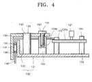
- FIG. 4 is a schematic enlarged cross-sectional view taken along line IV-IV of FIG. 3.
- the plasma display module 100 comprises a plasma display panel (PDP) 110 for realizing an image, a driving device 120, a chassis 130, a signal transmission unit 140, and a cover plate 150.
- PDP plasma display panel
- the PDP 110 is installed at the chassis 130.
- the PDP 110 and the chassis 130 are combined with each other using a double-faced adhesive 160 attached to the rear side of the PDP 110.
- a double-faced tape may be used as the double-faced adhesive 160.
- a panel heat-dissipation sheet 170 having high thermal conductivity is interposed between the PDP 110 and the chassis 130 so that heat generated during an operation of the PDP 110 can be prevented from being locally concentrated and heat-dissipation can be easily performed.
- the driving device 120 comprises a circuit element 121 and a circuit board 122.
- the circuit board 122 comprises an address electrode buffer circuit board 122a, an X-electrode driving circuit board 122b, a Y-electrode driving circuit board 122c, a power supply board 122d, and a logic control board 122e.
- a plurality of circuit elements 121 are disposed on the circuit board 122.
- the address electrode buffer circuit board 122a will be described.
- the address electrode buffer circuit board 122a is installed on a chassis base 131 by using a circuit board installation boss 133 and a circuit board installation bolt 181.
- a connector 123 is disposed on the address electrode buffer circuit board 122a so as to be electrically connected to the signal transmission unit 140.
- the chassis 130 is formed of aluminum and comprises a chassis base 131 and at least one chassis flange 132.
- the chassis 130 according to the present embodiment is formed of aluminum but the present invention is not limited to this. That is, there is no specific limitation in a material used in forming the chassis 130 according to the present invention and for example, the chassis 130 may be formed of iron or synthetic resin or the like.
- the chassis base 131 constitutes the greater part of the chassis 130.
- a plurality of circuit board installation bosses 133, a plurality of cover plate installation bosses 134, and a plurality of guide bosses 135 are formed on the chassis base 131.
- circuit board installation bosses 133 are used to install (mount) the circuit board 122 and correspond to a portion of the chassis base 131 in which the circuit board 122 is to be installed.
- the cover plate installation bosses 134 are used to install (mount) the cover plate 150 and are formed at edges of the chassis base 131.
- Each of the circuit board installation bosses 133 and each of the cover plate installation bosses 134 comprise a threaded tap hole and can be combined with the circuit board installation bolt 181 and the cover plate installation bolt 182, respectively.
- the guide bosses 135, used to prevent inclination of the cover plate 150 and to help installation of the cover plate 150, are formed near edges of the chassis base 131 adjacent to flanges 132, and may be adjacent to and paired with the cover plate installation bosses 134.
- Each of the guide bosses 135 is formed to have a height at which each guide boss 135 is inserted in a guide hole 152 of the cover plate 150.
- each guide boss 135 does not comprise a threaded tap hole, unlike the circuit board installation bosses 133 and the cover plate installation bosses 134.
- the chassis flange 132 is positioned at an edge of the chassis 130 and is bent to a similar height to the height of the circuit board 122.
- a cable such as a tape carrier package (TCP) or a chip on film (COF), is used as the signal transmission unit 140 for electrically connecting the PDP 110 and the address electrode buffer circuit board 122a.
- TCP tape carrier package
- COF chip on film
- the signal transmission unit 140 for transmitting an address signal passes a side of the chassis flange 132.
- One end of the signal transmission unit 140 is connected to the connector 123 installed on the address electrode buffer circuit board 122a, and the other end thereof passes the chassis flange 132 and is connected to the PDP 110.
- an integrated circuit chip 141 is installed in the signal transmission unit 140.
- the integrated circuit chip 141 controls an electrical signal that flows through the signal transmission unit 140.
- the integrated circuit chip 141 is installed on the chassis flange 132 of the chassis 130.
- the integrated circuit chip 141 is installed on the chassis flange 132 but the present invention is not limited to this. That is, according to embodiments of the present invention, when the chassis 130 comprises a reinforcement for reinforcing rigidity of the chassis base 131, the integrated circuit chip 141 may be installed on the reinforcement. In the present case, the chassis flange 132 provides reinforcement and rigidity to the chassis base 131.
- a thermal grease 190 is interposed between the integrated circuit chip 141 and the chassis flange 132.
- the thermal grease 190 is installed between the integrated circuit chip 141 and the chassis flange 132.
- the present invention is not limited to this. That is, according to embodiments of the present invention, the integrated circuit chip 141 may be directly in contact with the chassis flange 132 in the state where there is no thermal conduction medium such as the thermal grease 190, or a chip heat-dissipation sheet formed of a material having high thermal conductivity may be interposed between the integrated circuit chip 141 and the chassis flange 132.
- the cover plate 150 is formed to have a 'L' shape having a curved inner angle of 90 degrees and includes aluminum and iron or the like, having high thermal conductivity.
- the cover plate 150 protects the signal transmission unit 140 and the integrated circuit chip 141 and dissipates heat generated in the integrated circuit chip 141.
- the cover plate 150 is installed on the cover plate installation boss 134 formed on the chassis base 131. To this end, an installation hole 151 is formed in the cover plate 150. The size of the installation hole 151 is smaller than the size of an upper end of the cover plate installation boss 134 so that the cover plate 150 is placed above the cover plate installation boss 134 and then is secured and removably mounted by the cover plate installation bolt 182.
- a worker passes the cover plate installation bolt 182 through the installation hole 151 and combines the cover plate installation bolt 182 with a threaded tap hole 134a of the cover plate installation boss 134 so that the cover plate 150 can be installed on the cover plate installation boss 134.
- the guide hole 152 is formed in the cover plate 150 to be adjacent to the installation hole 151.
- the guide hole 152 is formed in such a way that the guide boss 135 is inserted in the guide hole 152.
- the guide hole 152 is preferably formed through the cover plate 150.
- the size of the guide hole 152 is formed in such a way that the guide hole 152 is fitted to the guide boss 135.
- fitting of the guide hole 152 and the guide boss 135 may be slide fit, or tight or interference fit.
- an inner circumferential surface of the guide hole 152 is the same as the thickness of the cover plate 150, when the guide hole 152 is inserted on the guide boss 135, the inner circumferential surface of the guide hole 152 contacts the guide boss 135 and serves as a guide. Then, an inclination for installing the cover plate 150 can be adjusted within an allowable limit desired by a designer.
- a portion of the cover plate 150 in which the installation hole 151 and the guide hole 152 are formed can be in parallel to the chassis base 131 and a portion of the cover plate 150 which corresponds to the integrated circuit chip 141 can be in parallel to the integrated circuit chip 141 and the chassis flange 132.
- the cover plate 150 is not inclined with respect to one surface of the integrated circuit chip 141 and is in parallel thereto, force, if any, that acts on the integrated circuit chip 141 by the cover plate 150 is uniform. Then, partial stress concentration can be prevented so that damage of the integrated circuit chip 141 can be prevented.
- the guide hole 152 is formed to have a circular shape and the cross-section of the guide boss 135 is also formed to have a circular shape.
- the present invention is not limited to this. That is, the shapes of the guide hole and the guide boss according to embodiments of the present invention are not limited only if the guide hole and the guide boss are inserted in each other, allow the position of the cover plate to be in parallel to the integrated circuit chip and damage of the integrated circuit chip is prevented.
- the guide hole may be formed to have a hexagonal shape and the cross-section of the guide boss may also be formed to have a hexagonal shape accordingly.
- a chip heat-dissipation sheet 195 formed of a material having high thermal conductivity is interposed between the integrated circuit chip 141 and the cover plate 150.
- the chip heat-dissipation sheet 195 transmits heat generated in the integrated circuit chip 141 to the cover plate 150.
- the chip heat-dissipation sheet 195 is installed between the integrated circuit chip 141 and the cover plate 150.
- the integrated circuit chip 141 may be directly in contact with the cover plate 150 in the state where there is no thermal conduction medium such as the chip heat-dissipation sheet 195 or a thermal grease having high thermal conductivity may be interposed between the integrated circuit chip 141 and the cover plate 150.
- the worker can install the cover plate 150 according to embodiments of the present embodiment using the following method.
- the user applies the thermal grease 190 on the chassis flange 132 and properly disposes the signal transmission unit 140 so that the integrated circuit chip 141 can be positioned on the applied thermal grease 190.
- the worker places the chip heat-dissipation sheet 195 between the integrated circuit chip 141 and the cover plate 150 and then, installs the cover plate 150 on the cover plate installation boss 134.
- the worker inserts the guide hole 152 of the cover plate 150 on the guide boss 135, passes the cover plate installation bolt 182 through the installation hole 151, and combines the cover plate installation bolt 182 with a threaded tap hole 134a of the cover plate installation boss 134.
- the cover plate 150 is not inclined with respect to the integrated circuit chip 141 and is precisely and rapidly installed as designed so that damage of the integrated circuit chip 141 can be prevented.
- the driving device 120 When the user operates the plasma display module 100, the driving device 120 is driven and a voltage is applied to the PDP 110.
- the energy level of the excited discharge gas during the sustain discharge is reduced and UV rays are emitted.
- the UV rays excite phosphor of a phosphor layer applied within discharge cells.
- the energy level of the excited phosphor is reduced, visible rays are emitted, and the visible rays are emitted so that an image that can be recognized by the user can be formed.
- the heat generated in the integrated circuit chip 141 and transmitted to the cover plate 150 is directly dissipated by convection heat transmission through the air that contacts the cover plate 150.
- the guide boss 135 and the guide hole 152 are assembled such that the cover plate 150 is prevented from being inclined with respect to the integrated circuit chip 141 and damage of the integrated circuit chip 141 is prevented.
- a process in which the worker checks the state where screws of the cover plate installation bolt 182 and the cover plate installation boss 134 are well engaged with each other and checks inclination for installing the cover plate 150 can be omitted such that the number of processes required to install the cover plate 150 and an assembling time are reduced.
- the plasma display module according to the present invention comprises the guide boss and the guide hole such that inclination of the cover plate with respect to the integrated circuit chip is prevented and the cover plate is rapidly installed. As such, damage of the integrated circuit chip of the signal transmission unit is prevented, and the number of processes required to install the cover plate and a working time are reduced.
Landscapes
- Engineering & Computer Science (AREA)
- Microelectronics & Electronic Packaging (AREA)
- Physics & Mathematics (AREA)
- Plasma & Fusion (AREA)
- Devices For Indicating Variable Information By Combining Individual Elements (AREA)
Abstract
Description
- The present invention relates to a plasma display module, and more particularly, to a plasma display module which prevents damage of an integrated circuit chip of a signal transmission unit by preventing a cover plate from being inclined during an assembling process of the cover plate.
- Plasma display panels (PDP) which come into the spotlight for replacing conventional cathode ray tube (CRT) display apparatuses, are flat display devices in which a discharge gas is sealed between two substrates in which a plurality of electrodes are formed, and then a discharge voltage is applied, and a phosphor layer formed in a predetermined pattern is excited by ultraviolet rays generated in a discharge processor, the phosphor layer then emits visible rays, and desired images are obtained.
- A plasma display device includes a plasma display module. In general, the plasma display module includes a plasma display panel (PDP) and a driving device for driving the plasma display panel (PDP).
- The driving device includes a circuit element and a circuit board on which the circuit element is disposed. The circuit board is electrically connected to the PDP by using the signal transmission unit. A plurality of wires extend in the lengthwise direction of the signal transmission unit. An integrated circuit chip is installed in part of a signal transmission unit.
- The integrated circuit chip installed in the signal transmission unit is disposed on a flange positioned at an edge of a chassis or is disposed to a reinforcement installed on the chassis. A large amount of heat is generated from the integrated circuit chip when the PDP is driven.
- Thus, a conventional plasma display module includes a cover plate installed to be closely adhered to the integrated circuit chip, thereby effectively dissipating heat generated from the integrated circuit chip.
- The cover plate is installed on the chassis using a boss or the like. Since the cover plate is installed to be closely adhered to the integrated circuit chip, a portion of the cover plate that is closely adhered to the integrated circuit chip must be installed in parallel to the integrated circuit chip. This is because, when the portion of the cover plate that is closely adhered to the integrated circuit chip is inclined to the integrated circuit chip, the integrated circuit chip is asymmetrically pressed by the cover plate and may be damaged by excessive stress concentration.
- The present invention provides a plasma display module which prevents damage of an integrated circuit chip of a signal transmission unit by preventing a cover plate from being inclined during an assembling process of the cover plate.
- According to an aspect of the present invention, there is provided a plasma display module as set out in Claim 1. Preferred features of this aspect are set out in Claims 2 to 13.
- A more complete appreciation of the invention and many of the attendant advantages thereof, will be readily apparent as the same becomes better understood by reference to the following detailed description when considered in conjunction with the accompanying drawings in which like reference symbols indicate the same or similar components, wherein:
- FIG. 1 is a schematic view illustrating the case where a conventional cover plate is inclined with respect to an integrated circuit chip of a signal transmission unit so that stress is concentrated on portion A of the integrated circuit chip;
- FIG. 2 is a schematic exploded perspective view of a plasma display module according to an embodiment of the present invention;
- FIG. 3 is an exploded perspective view illustrating an enlarged chassis portion of FIG. 2; and
- FIG. 4 is a schematic enlarged cross-sectional view taken along line IV-IV of FIG. 3.
- The present invention will now be described more fully with reference to the accompanying drawings, in which exemplary embodiments of the invention are shown.
- FIG. 1 is a schematic view illustrating the case where a cover plate is inclined with respect to an integrated circuit chip of a signal transmission unit so that stress is concentrated on portion A of the integrated
circuit chip 31. - As illustrated in FIG. 1, a
cover plate 10 is installed on achassis 20, and anintegrated circuit chip 31 of asignal transmission unit 30 is attached to thechassis 20 using an adhesive 40. - Here, the
cover plate 10 is installed to be inclined with respect to theintegrated circuit chip 31 so that portion A of theintegrated circuit chip 31 is excessively pressed by thecover plate 10 and stress is concentrated on portion A. When stress is excessively concentrated in this way, theintegrated circuit chip 30 may be damaged so that an increase in a defective rate occur increasing manufacturing costs. - Therefore, a worker must perform a variety of processes such as checking the state where screws of a bolt and a boss for fixing the cover plate are well engaged with each other so as to prevent the cover plate from being inclined with respect to the integrated circuit chip during a process of installing the cover plate, checking other factors for generating inclination of the cover plate, and checking an inclination degree of the finally-assembled cover plate. Thus, the time necessary to manufacture the device is increased accordingly and manufacturing costs increase.
- FIG. 2 is a schematic exploded perspective view of a plasma display module according to an embodiment of the present invention, FIG. 3 is an exploded perspective view illustrating an enlarged chassis portion of FIG. 2, and FIG. 4 is a schematic enlarged cross-sectional view taken along line IV-IV of FIG. 3.
- As illustrated in FIG. 2, the
plasma display module 100 according to an embodiment of the present invention comprises a plasma display panel (PDP) 110 for realizing an image, adriving device 120, achassis 130, asignal transmission unit 140, and acover plate 150. - The PDP 110 is installed at the
chassis 130. The PDP 110 and thechassis 130 are combined with each other using a double-faced adhesive 160 attached to the rear side of thePDP 110. A double-faced tape may be used as the double-faced adhesive 160. - A panel heat-
dissipation sheet 170 having high thermal conductivity is interposed between thePDP 110 and thechassis 130 so that heat generated during an operation of thePDP 110 can be prevented from being locally concentrated and heat-dissipation can be easily performed. - The
driving device 120 comprises acircuit element 121 and acircuit board 122. - The
circuit board 122 comprises an address electrodebuffer circuit board 122a, an X-electrodedriving circuit board 122b, a Y-electrodedriving circuit board 122c, apower supply board 122d, and alogic control board 122e. A plurality ofcircuit elements 121 are disposed on thecircuit board 122. In the present embodiment, the address electrodebuffer circuit board 122a will be described. - The address electrode
buffer circuit board 122a is installed on achassis base 131 by using a circuitboard installation boss 133 and a circuitboard installation bolt 181. - A
connector 123 is disposed on the address electrodebuffer circuit board 122a so as to be electrically connected to thesignal transmission unit 140. - The
chassis 130 is formed of aluminum and comprises achassis base 131 and at least onechassis flange 132. - The
chassis 130 according to the present embodiment is formed of aluminum but the present invention is not limited to this. That is, there is no specific limitation in a material used in forming thechassis 130 according to the present invention and for example, thechassis 130 may be formed of iron or synthetic resin or the like. - The
chassis base 131 constitutes the greater part of thechassis 130. A plurality of circuitboard installation bosses 133, a plurality of coverplate installation bosses 134, and a plurality ofguide bosses 135 are formed on thechassis base 131. - Here, the circuit
board installation bosses 133 are used to install (mount) thecircuit board 122 and correspond to a portion of thechassis base 131 in which thecircuit board 122 is to be installed. - The cover
plate installation bosses 134 are used to install (mount) thecover plate 150 and are formed at edges of thechassis base 131. Each of the circuitboard installation bosses 133 and each of the coverplate installation bosses 134 comprise a threaded tap hole and can be combined with the circuitboard installation bolt 181 and the coverplate installation bolt 182, respectively. - The
guide bosses 135, used to prevent inclination of thecover plate 150 and to help installation of thecover plate 150, are formed near edges of thechassis base 131 adjacent toflanges 132, and may be adjacent to and paired with the coverplate installation bosses 134. - Each of the
guide bosses 135 is formed to have a height at which eachguide boss 135 is inserted in aguide hole 152 of thecover plate 150. In this embodiment, eachguide boss 135 does not comprise a threaded tap hole, unlike the circuitboard installation bosses 133 and the coverplate installation bosses 134. - The
chassis flange 132 is positioned at an edge of thechassis 130 and is bent to a similar height to the height of thecircuit board 122. - A cable, such as a tape carrier package (TCP) or a chip on film (COF), is used as the
signal transmission unit 140 for electrically connecting thePDP 110 and the address electrodebuffer circuit board 122a. - The
signal transmission unit 140 for transmitting an address signal passes a side of thechassis flange 132. One end of thesignal transmission unit 140 is connected to theconnector 123 installed on the address electrodebuffer circuit board 122a, and the other end thereof passes thechassis flange 132 and is connected to thePDP 110. - Meanwhile, an integrated
circuit chip 141 is installed in thesignal transmission unit 140. Theintegrated circuit chip 141 controls an electrical signal that flows through thesignal transmission unit 140. - The
integrated circuit chip 141 is installed on thechassis flange 132 of thechassis 130. - In the present embodiment, the
integrated circuit chip 141 is installed on thechassis flange 132 but the present invention is not limited to this. That is, according to embodiments of the present invention, when thechassis 130 comprises a reinforcement for reinforcing rigidity of thechassis base 131, theintegrated circuit chip 141 may be installed on the reinforcement. In the present case, thechassis flange 132 provides reinforcement and rigidity to thechassis base 131. - A
thermal grease 190 is interposed between theintegrated circuit chip 141 and thechassis flange 132. - In the present embodiment, the
thermal grease 190 is installed between theintegrated circuit chip 141 and thechassis flange 132. However, the present invention is not limited to this. That is, according to embodiments of the present invention, theintegrated circuit chip 141 may be directly in contact with thechassis flange 132 in the state where there is no thermal conduction medium such as thethermal grease 190, or a chip heat-dissipation sheet formed of a material having high thermal conductivity may be interposed between theintegrated circuit chip 141 and thechassis flange 132. - The
cover plate 150 is formed to have a 'L' shape having a curved inner angle of 90 degrees and includes aluminum and iron or the like, having high thermal conductivity. Thecover plate 150 protects thesignal transmission unit 140 and theintegrated circuit chip 141 and dissipates heat generated in theintegrated circuit chip 141. - The
cover plate 150 is installed on the coverplate installation boss 134 formed on thechassis base 131. To this end, aninstallation hole 151 is formed in thecover plate 150. The size of theinstallation hole 151 is smaller than the size of an upper end of the coverplate installation boss 134 so that thecover plate 150 is placed above the coverplate installation boss 134 and then is secured and removably mounted by the coverplate installation bolt 182. - That is, a worker passes the cover
plate installation bolt 182 through theinstallation hole 151 and combines the coverplate installation bolt 182 with a threadedtap hole 134a of the coverplate installation boss 134 so that thecover plate 150 can be installed on the coverplate installation boss 134. - In addition, the
guide hole 152 is formed in thecover plate 150 to be adjacent to theinstallation hole 151. - The
guide hole 152 is formed in such a way that theguide boss 135 is inserted in theguide hole 152. Theguide hole 152 is preferably formed through thecover plate 150. - The size of the
guide hole 152 is formed in such a way that theguide hole 152 is fitted to theguide boss 135. Here, fitting of theguide hole 152 and theguide boss 135 may be slide fit, or tight or interference fit. - Since the height of an inner circumferential surface of the
guide hole 152 is the same as the thickness of thecover plate 150, when theguide hole 152 is inserted on theguide boss 135, the inner circumferential surface of theguide hole 152 contacts theguide boss 135 and serves as a guide. Then, an inclination for installing thecover plate 150 can be adjusted within an allowable limit desired by a designer. - As such, a portion of the
cover plate 150 in which theinstallation hole 151 and theguide hole 152 are formed can be in parallel to thechassis base 131 and a portion of thecover plate 150 which corresponds to theintegrated circuit chip 141 can be in parallel to theintegrated circuit chip 141 and thechassis flange 132. - Through the above-described structure, since the
cover plate 150 is not inclined with respect to one surface of theintegrated circuit chip 141 and is in parallel thereto, force, if any, that acts on theintegrated circuit chip 141 by thecover plate 150 is uniform. Then, partial stress concentration can be prevented so that damage of theintegrated circuit chip 141 can be prevented. - According to the present embodiment, the
guide hole 152 is formed to have a circular shape and the cross-section of theguide boss 135 is also formed to have a circular shape. However, the present invention is not limited to this. That is, the shapes of the guide hole and the guide boss according to embodiments of the present invention are not limited only if the guide hole and the guide boss are inserted in each other, allow the position of the cover plate to be in parallel to the integrated circuit chip and damage of the integrated circuit chip is prevented. For example, the guide hole may be formed to have a hexagonal shape and the cross-section of the guide boss may also be formed to have a hexagonal shape accordingly. - A chip heat-
dissipation sheet 195 formed of a material having high thermal conductivity is interposed between theintegrated circuit chip 141 and thecover plate 150. The chip heat-dissipation sheet 195 transmits heat generated in theintegrated circuit chip 141 to thecover plate 150. - In the present embodiment, the chip heat-
dissipation sheet 195 is installed between theintegrated circuit chip 141 and thecover plate 150. However, embodiments of the present invention are not limited to this. That is, according to embodiments of the present invention, theintegrated circuit chip 141 may be directly in contact with thecover plate 150 in the state where there is no thermal conduction medium such as the chip heat-dissipation sheet 195 or a thermal grease having high thermal conductivity may be interposed between theintegrated circuit chip 141 and thecover plate 150. - The worker can install the
cover plate 150 according to embodiments of the present embodiment using the following method. - That is, the user applies the
thermal grease 190 on thechassis flange 132 and properly disposes thesignal transmission unit 140 so that theintegrated circuit chip 141 can be positioned on the appliedthermal grease 190. - Next, the worker places the chip heat-
dissipation sheet 195 between theintegrated circuit chip 141 and thecover plate 150 and then, installs thecover plate 150 on the coverplate installation boss 134. - In this case, the worker inserts the
guide hole 152 of thecover plate 150 on theguide boss 135, passes the coverplate installation bolt 182 through theinstallation hole 151, and combines the coverplate installation bolt 182 with a threadedtap hole 134a of the coverplate installation boss 134. As such, thecover plate 150 is not inclined with respect to theintegrated circuit chip 141 and is precisely and rapidly installed as designed so that damage of theintegrated circuit chip 141 can be prevented. - An operation of operating the
plasma display module 100 according to embodiments of the present embodiment and a dissipation path of heat generated in theintegrated circuit chip 141 will now be described. - When the user operates the
plasma display module 100, the drivingdevice 120 is driven and a voltage is applied to thePDP 110. - When the voltage is applied to the
PDP 110, an address discharge and a sustain discharge occur, the energy level of the excited discharge gas during the sustain discharge is reduced and UV rays are emitted. The UV rays excite phosphor of a phosphor layer applied within discharge cells. The energy level of the excited phosphor is reduced, visible rays are emitted, and the visible rays are emitted so that an image that can be recognized by the user can be formed. - In this case, a large amount of heat is generated in the
integrated circuit chip 141 installed in thesignal transmission unit 140. Part of the heat is transmitted to thechassis flange 132 via thethermal grease 190 and other part of the heat is transmitted to thecover plate 150 via the chip heat-dissipation sheet 195. - The heat generated in the
integrated circuit chip 141 and transmitted to thecover plate 150 is directly dissipated by convection heat transmission through the air that contacts thecover plate 150. - As described above, in the
plasma display module 100 according to embodiments of the present invention, when thecover plate 150 is installed, theguide boss 135 and theguide hole 152 are assembled such that thecover plate 150 is prevented from being inclined with respect to theintegrated circuit chip 141 and damage of theintegrated circuit chip 141 is prevented. - In addition, according to embodiments of the present invention, a process in which the worker checks the state where screws of the cover
plate installation bolt 182 and the coverplate installation boss 134 are well engaged with each other and checks inclination for installing thecover plate 150 can be omitted such that the number of processes required to install thecover plate 150 and an assembling time are reduced. - As described above, the plasma display module according to the present invention comprises the guide boss and the guide hole such that inclination of the cover plate with respect to the integrated circuit chip is prevented and the cover plate is rapidly installed. As such, damage of the integrated circuit chip of the signal transmission unit is prevented, and the number of processes required to install the cover plate and a working time are reduced.
- While the present invention has been particularly shown and described with reference to exemplary embodiments thereof, it will be understood by those of ordinary skill in the art that various changes in form and details may be made therein without departing from the scope of the present invention as defined by the following claims.
Claims (13)
- A plasma display module comprising:a plasma display panel, PDP, for realizing an image;a driving device for driving the PDP;a chassis for supporting the PDP and the driving device, the chassis including at least one guide boss;a signal transmission unit electrically for connecting the PDP and the driving device, the signal transmission unit including an integrated circuit chip; anda cover plate installed to face the integrated circuit chip, said cover plate including at least one guide hole through which the guide boss is inserted wherein said at least one guide boss is arranged to prevent the cover plate from being inclined with respect to the integrated circuit chip.
- A plasma display module according to claim 1, wherein the driving device comprises a circuit element and a circuit board on which the circuit element is disposed.
- A plasma display module according to claim 1 or 2, wherein the signal transmission unit is a TCP (tape carrier package) or a COF (chip on film).
- A plasma display module according to any one of claims 1 to 3, wherein the integrated circuit chip is in contact with a flange portion of said chassis.
- A plasma display module according to claim 4, wherein a chip heat-dissipation sheet is interposed between the integrated circuit chip and the flange portion of said chassis.
- A plasma display module according to claim 4 or 5, wherein a thermal grease is interposed between the integrated circuit chip and the flange portion of said chassis.
- A plasma display module according to any one of claims 1 to 6, wherein a chip heat-dissipation sheet is interposed between the integrated circuit chip and the cover plate.
- A plasma display module according to any one of claims 1 to 7, wherein a thermal grease is interposed between the integrated circuit chip and the cover plate.
- A plasma display module according to any one of claims 1 to 8, wherein at least one cover plate installation boss for installing the cover plate is formed on the chassis, and at least one installation hole corresponding to the cover plate installation boss is formed in the cover plate.
- A plasma display module according to claim 9, wherein the cover plate is securely mounted to the cover plate installation boss using a cover plate installation bolt.
- A plasma display module according to any one of claims 1 to 8, which said chassis including at least one pair of a said guide boss and an adjacent cover plate installation boss, and
said cover plate includes at least one installation hole through which a cover plate installation bolt is inserted to connect with a said cover plate installation boss. - A plasma display module according to claim 11, wherein said chassis comprises a plurality of pairs of guide bosses and adjacent cover plate installation bosses.
- A plasma display module according to claim 11 or 12, wherein said chassis comprises a first plurality of pairs of guide bosses and adjacent cover plate installation bosses on one end of said chassis, and a second plurality of pairs of guide bosses and adjacent cover plate installation bosses on an opposite end of said chassis.
Applications Claiming Priority (1)
| Application Number | Priority Date | Filing Date | Title |
|---|---|---|---|
| KR1020060088682A KR100813843B1 (en) | 2006-09-13 | 2006-09-13 | Plasma display module |
Publications (2)
| Publication Number | Publication Date |
|---|---|
| EP1901597A1 true EP1901597A1 (en) | 2008-03-19 |
| EP1901597B1 EP1901597B1 (en) | 2009-06-24 |
Family
ID=38779862
Family Applications (1)
| Application Number | Title | Priority Date | Filing Date |
|---|---|---|---|
| EP07253649A Not-in-force EP1901597B1 (en) | 2006-09-13 | 2007-09-13 | Plasma display module |
Country Status (6)
| Country | Link |
|---|---|
| US (1) | US20080062628A1 (en) |
| EP (1) | EP1901597B1 (en) |
| JP (1) | JP4612029B2 (en) |
| KR (1) | KR100813843B1 (en) |
| CN (1) | CN101145302A (en) |
| DE (1) | DE602007001371D1 (en) |
Families Citing this family (5)
| Publication number | Priority date | Publication date | Assignee | Title |
|---|---|---|---|---|
| KR101494849B1 (en) * | 2008-06-13 | 2015-02-24 | 삼성디스플레이 주식회사 | Backlight assembly and display device including the same |
| KR101030990B1 (en) * | 2008-12-31 | 2011-04-22 | 삼성에스디아이 주식회사 | Semiconductor package and plasma display device having same |
| CN105163563B (en) * | 2015-08-27 | 2018-04-17 | 苏州佳世达电通有限公司 | Display device |
| CN110189650A (en) * | 2019-05-29 | 2019-08-30 | 厦门天马微电子有限公司 | Display module and display device |
| KR20220069173A (en) * | 2020-11-19 | 2022-05-27 | 삼성디스플레이 주식회사 | Protective cap and display device including same |
Citations (6)
| Publication number | Priority date | Publication date | Assignee | Title |
|---|---|---|---|---|
| US20050011664A1 (en) | 2003-07-16 | 2005-01-20 | Chang-Chi Lee | Structure of a cable |
| US20050031492A1 (en) | 2003-07-10 | 2005-02-10 | Sysmex Corporation | Electronic device, analysis system, and conveyance device |
| US20050116644A1 (en) * | 2003-11-27 | 2005-06-02 | Ki-Jung Kim | Plasma display apparatus |
| US20050174726A1 (en) * | 2003-10-16 | 2005-08-11 | Heung-Chul Bang | Display apparatus having stress-diffusing means |
| US20050212982A1 (en) | 2004-03-10 | 2005-09-29 | Kabushiki Kaisha Toshiba | Display apparatus |
| US20060152909A1 (en) | 2001-06-15 | 2006-07-13 | Tomihide Nomoto | Plasma display apparatus |
Family Cites Families (24)
| Publication number | Priority date | Publication date | Assignee | Title |
|---|---|---|---|---|
| JPH0410620Y2 (en) * | 1985-12-28 | 1992-03-16 | ||
| JP3656455B2 (en) * | 1999-04-13 | 2005-06-08 | 富士電機デバイステクノロジー株式会社 | Driver module structure |
| JP3973345B2 (en) * | 2000-06-05 | 2007-09-12 | 富士通日立プラズマディスプレイ株式会社 | Plasma display device |
| KR100484105B1 (en) * | 2002-09-14 | 2005-04-19 | 삼성에스디아이 주식회사 | Mounting boss for circuit board and base chassis therewith |
| JP3778507B2 (en) * | 2002-11-28 | 2006-05-24 | 横浜ゴム株式会社 | Curing agent composition and curable resin composition containing the same |
| JP4186649B2 (en) * | 2003-02-27 | 2008-11-26 | 松下電器産業株式会社 | Plasma display device |
| KR20050060118A (en) * | 2003-12-15 | 2005-06-22 | 주식회사 대우일렉트로닉스 | Structure for combining the front cabinet and the back cover of the plasma displaying device |
| US7508673B2 (en) * | 2004-03-04 | 2009-03-24 | Samsung Sdi Co., Ltd. | Heat dissipating apparatus for plasma display device |
| KR100612278B1 (en) * | 2004-05-18 | 2006-08-11 | 삼성에스디아이 주식회사 | Plasma display device |
| KR100626012B1 (en) * | 2004-06-30 | 2006-09-20 | 삼성에스디아이 주식회사 | Plasma display device |
| KR100615246B1 (en) * | 2004-08-28 | 2006-08-25 | 삼성에스디아이 주식회사 | Plasma display device |
| KR100669729B1 (en) * | 2004-09-21 | 2007-01-16 | 삼성에스디아이 주식회사 | Plasma display device |
| KR100615299B1 (en) * | 2004-12-17 | 2006-08-25 | 삼성에스디아이 주식회사 | Plasma display assembly |
| KR100670268B1 (en) * | 2005-01-14 | 2007-01-16 | 삼성에스디아이 주식회사 | Display device |
| KR100846584B1 (en) | 2005-02-05 | 2008-07-16 | 삼성에스디아이 주식회사 | Exhaust Pipe Protection Tip Structure and Plasma Display Module |
| KR100637214B1 (en) * | 2005-02-19 | 2006-10-23 | 삼성에스디아이 주식회사 | Cover plate mounting structure and plasma display module having same |
| KR100637492B1 (en) * | 2005-02-22 | 2006-10-20 | 삼성에스디아이 주식회사 | Plasma display device |
| KR100717784B1 (en) * | 2005-02-24 | 2007-05-11 | 삼성에스디아이 주식회사 | Plasma display device |
| KR100696517B1 (en) * | 2005-05-02 | 2007-03-19 | 삼성에스디아이 주식회사 | Integrated circuit chip heat dissipation structure of plasma display module and plasma display module having same |
| JP4893035B2 (en) * | 2006-03-17 | 2012-03-07 | 株式会社日立製作所 | Flat panel display |
| KR100759574B1 (en) * | 2006-04-11 | 2007-09-18 | 삼성에스디아이 주식회사 | Plasma display |
| KR100839412B1 (en) * | 2006-11-27 | 2008-06-19 | 삼성에스디아이 주식회사 | Plasma display device |
| KR20080067928A (en) * | 2007-01-17 | 2008-07-22 | 삼성에스디아이 주식회사 | Plasma display device |
| KR100989421B1 (en) * | 2009-01-06 | 2010-10-26 | 삼성에스디아이 주식회사 | Plasma display device |
-
2006
- 2006-09-13 KR KR1020060088682A patent/KR100813843B1/en not_active Expired - Fee Related
-
2007
- 2007-08-10 US US11/889,308 patent/US20080062628A1/en not_active Abandoned
- 2007-09-07 CN CNA2007101490563A patent/CN101145302A/en active Pending
- 2007-09-13 JP JP2007238035A patent/JP4612029B2/en not_active Expired - Fee Related
- 2007-09-13 DE DE602007001371T patent/DE602007001371D1/en active Active
- 2007-09-13 EP EP07253649A patent/EP1901597B1/en not_active Not-in-force
Patent Citations (6)
| Publication number | Priority date | Publication date | Assignee | Title |
|---|---|---|---|---|
| US20060152909A1 (en) | 2001-06-15 | 2006-07-13 | Tomihide Nomoto | Plasma display apparatus |
| US20050031492A1 (en) | 2003-07-10 | 2005-02-10 | Sysmex Corporation | Electronic device, analysis system, and conveyance device |
| US20050011664A1 (en) | 2003-07-16 | 2005-01-20 | Chang-Chi Lee | Structure of a cable |
| US20050174726A1 (en) * | 2003-10-16 | 2005-08-11 | Heung-Chul Bang | Display apparatus having stress-diffusing means |
| US20050116644A1 (en) * | 2003-11-27 | 2005-06-02 | Ki-Jung Kim | Plasma display apparatus |
| US20050212982A1 (en) | 2004-03-10 | 2005-09-29 | Kabushiki Kaisha Toshiba | Display apparatus |
Also Published As
| Publication number | Publication date |
|---|---|
| JP2008070879A (en) | 2008-03-27 |
| KR100813843B1 (en) | 2008-03-17 |
| DE602007001371D1 (en) | 2009-08-06 |
| CN101145302A (en) | 2008-03-19 |
| JP4612029B2 (en) | 2011-01-12 |
| EP1901597B1 (en) | 2009-06-24 |
| US20080062628A1 (en) | 2008-03-13 |
Similar Documents
| Publication | Publication Date | Title |
|---|---|---|
| US6494429B2 (en) | Panel support structure, display panel supported by panel support structure, and image forming apparatus using display panel | |
| US7372704B2 (en) | Heat dissipating structure for IC chip of plasma display module and plasma display module having the same | |
| US7394186B2 (en) | Display apparatus | |
| EP1901597B1 (en) | Plasma display module | |
| US7463490B2 (en) | Plasma display apparatus | |
| US7619891B2 (en) | Plasma display apparatus | |
| KR100730136B1 (en) | Integrated circuit chip heat dissipation structure of plasma display module and plasma display module having same | |
| US20090180042A1 (en) | Display apparatus | |
| KR100749621B1 (en) | Plasma display | |
| KR100884800B1 (en) | Flat panel display module | |
| EP1727181A1 (en) | Plasma display apparatus | |
| KR20030034764A (en) | Plasma display device | |
| KR100696510B1 (en) | Integrated circuit chip heat dissipation structure of plasma display module and plasma display module having same | |
| KR100731457B1 (en) | Plasma display | |
| KR100759571B1 (en) | Plasma display device | |
| KR100659098B1 (en) | Plasma display module | |
| KR100669784B1 (en) | Flat panel display module | |
| KR100637192B1 (en) | Flat panel display module | |
| KR20060100769A (en) | Cover plate mounting structure and plasma display module having same | |
| KR100615886B1 (en) | Plasma display device | |
| KR20080044139A (en) | Plasma display device | |
| KR20060100770A (en) | Integrated circuit chip heat dissipation structure of plasma display module | |
| KR20060090437A (en) | Plasma display device | |
| KR20080039743A (en) | Plasma display device | |
| KR20060090443A (en) | Heat dissipation structure of chassis base in display panel module |
Legal Events
| Date | Code | Title | Description |
|---|---|---|---|
| PUAI | Public reference made under article 153(3) epc to a published international application that has entered the european phase |
Free format text: ORIGINAL CODE: 0009012 |
|
| 17P | Request for examination filed |
Effective date: 20070921 |
|
| AK | Designated contracting states |
Kind code of ref document: A1 Designated state(s): AT BE BG CH CY CZ DE DK EE ES FI FR GB GR HU IE IS IT LI LT LU LV MC MT NL PL PT RO SE SI SK TR |
|
| AX | Request for extension of the european patent |
Extension state: AL BA HR MK YU |
|
| RIN1 | Information on inventor provided before grant (corrected) |
Inventor name: KIM, MYOUNG-KON Inventor name: BANG, WON-KYU |
|
| AKX | Designation fees paid |
Designated state(s): DE FR GB |
|
| GRAP | Despatch of communication of intention to grant a patent |
Free format text: ORIGINAL CODE: EPIDOSNIGR1 |
|
| RIN1 | Information on inventor provided before grant (corrected) |
Inventor name: BANG, WON-KYU Inventor name: KIM, MYOUNG-KON |
|
| GRAS | Grant fee paid |
Free format text: ORIGINAL CODE: EPIDOSNIGR3 |
|
| GRAA | (expected) grant |
Free format text: ORIGINAL CODE: 0009210 |
|
| AK | Designated contracting states |
Kind code of ref document: B1 Designated state(s): DE FR GB |
|
| REG | Reference to a national code |
Ref country code: GB Ref legal event code: FG4D |
|
| REF | Corresponds to: |
Ref document number: 602007001371 Country of ref document: DE Date of ref document: 20090806 Kind code of ref document: P |
|
| PLBE | No opposition filed within time limit |
Free format text: ORIGINAL CODE: 0009261 |
|
| STAA | Information on the status of an ep patent application or granted ep patent |
Free format text: STATUS: NO OPPOSITION FILED WITHIN TIME LIMIT |
|
| 26N | No opposition filed |
Effective date: 20100325 |
|
| PGFP | Annual fee paid to national office [announced via postgrant information from national office to epo] |
Ref country code: DE Payment date: 20130626 Year of fee payment: 7 |
|
| PGFP | Annual fee paid to national office [announced via postgrant information from national office to epo] |
Ref country code: FR Payment date: 20130718 Year of fee payment: 7 Ref country code: GB Payment date: 20130719 Year of fee payment: 7 |
|
| REG | Reference to a national code |
Ref country code: DE Ref legal event code: R119 Ref document number: 602007001371 Country of ref document: DE |
|
| GBPC | Gb: european patent ceased through non-payment of renewal fee |
Effective date: 20140913 |
|
| REG | Reference to a national code |
Ref country code: DE Ref legal event code: R119 Ref document number: 602007001371 Country of ref document: DE Effective date: 20150401 |
|
| REG | Reference to a national code |
Ref country code: FR Ref legal event code: ST Effective date: 20150529 |
|
| PG25 | Lapsed in a contracting state [announced via postgrant information from national office to epo] |
Ref country code: DE Free format text: LAPSE BECAUSE OF NON-PAYMENT OF DUE FEES Effective date: 20150401 Ref country code: GB Free format text: LAPSE BECAUSE OF NON-PAYMENT OF DUE FEES Effective date: 20140913 |
|
| PG25 | Lapsed in a contracting state [announced via postgrant information from national office to epo] |
Ref country code: FR Free format text: LAPSE BECAUSE OF NON-PAYMENT OF DUE FEES Effective date: 20140930 |