EP1898472A1 - Avalanche photodiode - Google Patents
Avalanche photodiode Download PDFInfo
- Publication number
- EP1898472A1 EP1898472A1 EP06767417A EP06767417A EP1898472A1 EP 1898472 A1 EP1898472 A1 EP 1898472A1 EP 06767417 A EP06767417 A EP 06767417A EP 06767417 A EP06767417 A EP 06767417A EP 1898472 A1 EP1898472 A1 EP 1898472A1
- Authority
- EP
- European Patent Office
- Prior art keywords
- layer
- optical absorption
- type
- absorption layer
- electrode layer
- Prior art date
- Legal status (The legal status is an assumption and is not a legal conclusion. Google has not performed a legal analysis and makes no representation as to the accuracy of the status listed.)
- Granted
Links
Images

Classifications
-
- H—ELECTRICITY
- H10—SEMICONDUCTOR DEVICES; ELECTRIC SOLID-STATE DEVICES NOT OTHERWISE PROVIDED FOR
- H10F—INORGANIC SEMICONDUCTOR DEVICES SENSITIVE TO INFRARED RADIATION, LIGHT, ELECTROMAGNETIC RADIATION OF SHORTER WAVELENGTH OR CORPUSCULAR RADIATION
- H10F30/00—Individual radiation-sensitive semiconductor devices in which radiation controls the flow of current through the devices, e.g. photodetectors
- H10F30/20—Individual radiation-sensitive semiconductor devices in which radiation controls the flow of current through the devices, e.g. photodetectors the devices having potential barriers, e.g. phototransistors
- H10F30/21—Individual radiation-sensitive semiconductor devices in which radiation controls the flow of current through the devices, e.g. photodetectors the devices having potential barriers, e.g. phototransistors the devices being sensitive to infrared, visible or ultraviolet radiation
- H10F30/22—Individual radiation-sensitive semiconductor devices in which radiation controls the flow of current through the devices, e.g. photodetectors the devices having potential barriers, e.g. phototransistors the devices being sensitive to infrared, visible or ultraviolet radiation the devices having only one potential barrier, e.g. photodiodes
- H10F30/225—Individual radiation-sensitive semiconductor devices in which radiation controls the flow of current through the devices, e.g. photodetectors the devices having potential barriers, e.g. phototransistors the devices being sensitive to infrared, visible or ultraviolet radiation the devices having only one potential barrier, e.g. photodiodes the potential barrier working in avalanche mode, e.g. avalanche photodiodes
-
- H—ELECTRICITY
- H10—SEMICONDUCTOR DEVICES; ELECTRIC SOLID-STATE DEVICES NOT OTHERWISE PROVIDED FOR
- H10F—INORGANIC SEMICONDUCTOR DEVICES SENSITIVE TO INFRARED RADIATION, LIGHT, ELECTROMAGNETIC RADIATION OF SHORTER WAVELENGTH OR CORPUSCULAR RADIATION
- H10F30/00—Individual radiation-sensitive semiconductor devices in which radiation controls the flow of current through the devices, e.g. photodetectors
- H10F30/20—Individual radiation-sensitive semiconductor devices in which radiation controls the flow of current through the devices, e.g. photodetectors the devices having potential barriers, e.g. phototransistors
- H10F30/21—Individual radiation-sensitive semiconductor devices in which radiation controls the flow of current through the devices, e.g. photodetectors the devices having potential barriers, e.g. phototransistors the devices being sensitive to infrared, visible or ultraviolet radiation
- H10F30/22—Individual radiation-sensitive semiconductor devices in which radiation controls the flow of current through the devices, e.g. photodetectors the devices having potential barriers, e.g. phototransistors the devices being sensitive to infrared, visible or ultraviolet radiation the devices having only one potential barrier, e.g. photodiodes
- H10F30/225—Individual radiation-sensitive semiconductor devices in which radiation controls the flow of current through the devices, e.g. photodetectors the devices having potential barriers, e.g. phototransistors the devices being sensitive to infrared, visible or ultraviolet radiation the devices having only one potential barrier, e.g. photodiodes the potential barrier working in avalanche mode, e.g. avalanche photodiodes
- H10F30/2255—Individual radiation-sensitive semiconductor devices in which radiation controls the flow of current through the devices, e.g. photodetectors the devices having potential barriers, e.g. phototransistors the devices being sensitive to infrared, visible or ultraviolet radiation the devices having only one potential barrier, e.g. photodiodes the potential barrier working in avalanche mode, e.g. avalanche photodiodes in which the active layers form heterostructures, e.g. SAM structures
Definitions
- the present invention relates to an ultrafast avalanche photodiode operating at the long-wavelength used for optical communication, and, more particularly, the present invention relates a guard ring structure for securing a stable operation of an avalanche photodiode capable of ultrafast operation.
- the avalanche photodiode (hereafter referred to as APD) is a device utilized as a low-noise optical receiver, which generates carriers (electron and hole) by optical absorption, multiplies the carrier by an avalanche mechanism, and extract the output electrical signal from the carrier current.
- An APD operating at the long-wavelength has already been introduced widely to 2.5Gbit/s and 10Gbit/s systems, and a device which is applicable to the next-generation system with the rate of 40Gbit/s is in process of being developed.
- a hole-injection type APD having an InP avalanche multiplication layer has been commonly adopted as a relatively low-speed APD structure.
- an electron-injection type APD which is superior in terms of operation speed, has been attracting attention.
- a long-wavelength APD having an InGaAs optical absorption layer commonly employs an SAM (Separated Absorption and Multiplication) structure, in which an optical absorption layer and an avalanche multiplication layer (avalanche layer) are separated to suppress an increase of dark current induced by a narrow gap semiconductor.
- SAM Synchronated Absorption and Multiplication
- an electric-field control layer and a bandgap graded layer are provided between the optical absorption layer and the avalanche multiplication layer.
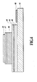
- Figure 4 is a cross-sectional view showing a conventional mesa-type APD.
- the electron-injection type APD shown in Figure 4 is configured to have an optical absorption layer 46 composed of a depleted InGaAs and an avalanche multiplication layer 43 composed of either InAlAs or InP.
- an electric-field control layer 44 and a bandgap graded layer 45 are provided between the avalanche multiplication layer 43 and the InGaAs optical absorption layer 46 which both are provided on an n-InP electrode layer 41.
- An InGaAs electrode layer 47 is formed on the optical absorption layer 46, and an electrode 49 is further formed thereon.
- An electrode 48 is also provided on the n-InP electrode layer 41.
- a guard ring structure which is formed by using a Zn diffusion technique cannot be adopted; therefore, a typical electron-injection type ADP is only allowed to have a mesa-type device structure as shown in Figure 4 . As a result, a fundamental problem arises in which dark current is increased around the junction periphery of the device.
- nonpatent document 1 a structure in which an InP regrown layer covers the area around the mesa structure of a device has been proposed (refer to nonpatent document 1), and good characteristics have been reported.
- nonpatent document 2 A structure in which electric field distribution is modulated around the operation region by ion implantation has also been reported (nonpatent document 2).
- nonpatent document 2 a structure in which a buffer layer including an n-type doped partial in-plane region is inserted between an avalanche multiplication layer and an n electrode layer so that the electric field intensity around the mesa becomes lower than that of the inside in operation.
- the electron-injection type APD demonstrates superior features to those of the conventional hole-injection type APD, there were problems in terms of an increase of dark current and securing the device life time.
- a structure has also been proposed in which a mesa is buried in APD by use of semiconductor; however, the problems in difficulty of the production technique and production cost still remain to be solved.
- the present invention aims to provide a production technique of an electron-injection type APD without using of a diffusion technique.
- the provide APD has to be capable of providing a stable operation with low dark current.
- a technique regarding a "guard ring structure" is applied to the present invention for the purpose of achieving stable operation of the electron-injection type APD. Detailed explanations will be provided in the following section.
- the invention described in claim 1 provides an avalanche photodiode.
- the avalanche photodiode is formed by sequentially laminating an n-type electrode layer, an avalanche multiplication layer, an electric field control layer, and a bandgap graded layer. On the bandgap graded layer, an optical absorption layer forming a mesa structure and a p-type electrode layer are sequentially formed.
- the avalanche photodiode is characterized by having a buffer layer and an n-type doping region. The buffer layer is formed between the n-type electrode layer and the avalanche multiplication layer.
- the n-type doping region having a substantially trapezoidal cross section area perpendicular to the laminated plane is formed on the inside of the interior portion of a region included in the interior portion of the buffer layer, having a contact with the n-type electrode layer, and having the mesa structure formed therein within the laminated plane.
- the two nodes between the p-type electrode layer and the n-type electrode layer are reversely biased, the vicinity portion of the upper hem in the substantially trapezoidal cross section area in the n-type doping region is approximately depleted.
- the invention described in claim 2 is characterized in that the n-type doping region has concentration distributions monotonically increasing from the avalanche multiplication layer towards the n-type electrode layer and from the peripheral region towards the center within the n-type doping region.
- the invention described in claim 3 is characterized by having a first p-type optical absorption layer which is formed underneath a p-type electrode, and a low-concentration second optical absorption layer which is formed between the first optical absorption layer and the bandgap graded layer, and is depleted when the p-type electrode layer and the n-type electrode layer are reversely biased.
- the invention described in claim 4 is characterized in that the second optical absorption layer has a thickness set to be the maximum thickness fulfilling the condition in which in-plane distribution of avalanche multiplication coefficient in the device monotonically decreases from the center to the peripheral direction within the n-type doping region.
- each of the avalanche multiplication layer, the optical absorption layer, the first optical absorption layer, and the second optical absorption layer is composed of an InP/InGaAsP-based compound semiconductor or an InAIGaAs-based compound semiconductor.
- the present invention it is possible to relax the edge electric field in the peripheral part of the avalanche multiplication region without using a diffusion technique, and therefore possible to produce an electron-injection type APD with low dark current in a highly controlled manner.
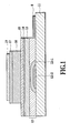
- Figure 1 is a structural drawing of an APD in accordance with a first embodiment of the present invention.
- an InP buffer layer 12 On an n-type InP electrode layer 11, an InP buffer layer 12, an InP avalanche multiplication layer 13, an InP electric field control layer 14, and an InGaAsP bandgap graded layer 15 are formed in order.
- an InGaAsP bandgap graded layer 15 On the InGaAsP bandgap graded layer 15, a p-type InGaAs optical absorption layer 16 in a mesa structure, a p-type InGaAsP electrode layer 17, and a metal electrode 18 are provided.
- a metal electrode 19 On the n-type InP electrode layer 11, a metal electrode 19 is also provided.
- n-type InP doping regions 12-1 and 12-2 are formed locally within the InP buffer layer 12.
- the n-type InP doping region 12-2 is included within the n-type InP doping region 12-1.
- the n-type InP doping regions 12-1 and 12-2 have different doping concentrations. The structure and the fabrication method will be explained in detail in the later section. As will hereinafter be explained, with allocation of the n-type InP doping regions 12-1 and 12-2, an APD structure is obtained in which the surrounding region of the n-type InP doping regions 12-1 and 12-2 functions as a "guard ring.”
- the n-type InP doping region 12-1 is arranged so that the n-type InP doping region 12-1 is located inside of the periphery of the mesa structure of the InGaAs optical absorption layer 16.
- the n-type InP doping region 12-1 is approximately a circular form or an oval figure.
- the type InP doping region 12-1 is arranged so that the periphery of the n-type InP doping region 12-1 is located within an area of the mesa-structure defined by the InGaAs optical absorption layer 16.
- the electric field intensity in the part which has no n-type InP doping region 12-1 being located immediately below is decreased with a certain level of voltage applied; thus, depletion of the mesa lateral side of the InGaAs optical absorption layer 16 is prevented.
- electric field generation can be prevented.
- the APD of the present invention provided with the guard ring structure including the n-type InP doping region 12-1 can be produced, for example, in the following manner. Firstly, in order to form an InP buffer layer 12, an n-InP layer which corresponds to the n-type InP electrode layer 11 is grown on an InP substrate, and then undoped InP crystals are grown to form an undoped InP layer on the n-InP layer. After the formation of the buffer layer 12, the n-type InP doping regions 12-1 and 12-2 are formed by Si ion implantation.
- the InP electric field control layer 14 carries out a function to adjust the difference of electric fields between the bandgap graded layer 15 and the part adjacent to the bandgap graded layer 15 within the InGaAs optical absorption layer 16 to a predetermined value.
- the n-type doping region 12-1 can be seen as a substantially trapezoidal form with a round portion around the upper hem in the cross-sectional surface perpendicular to the laminated planes of the APD layers, as shown in Figure 1 .
- a convex-trapezoidal n-type doping region 12-1 is introduced, local electric field concentration is prone to be generated in the part located on the side of InP avalanche multiplication layer 13.
- Figure 5 shows electric field concentration when a buried n-type InP region is provided in the buffer layer.
- the basic structure of the APD shown in Figure 5 is the same as that shown in Figure 1 .
- Difference between Figures 1 and 5 is that the structure shown in Figure 5 is provided with the buried n-type InP region 52-1 in the buffer layer 52.
- local electric field concentration indicated by the arrows is generated in the surrounding part of the buried n-type InP region 52-1 in the side of the avalanche multiplication layer 53.
- the present invention has the following characteristics. Specifically, the n-type InP doping region 12-1 has doping concentration distribution. In addition, in the surrounding part of the n-type doping region 12, the depleted region penetrates sufficiently deeply into the inside of the n-type InP doping region 12-1. A potential drop is generated in the part which the depleted region penetrates into.
- the potential drop can prevent an electric field increase in the upper side, that is, in the side of the InP avalanche multiplication layer 13, of the part in which the potential drop is generated; thus, it is possible to relax "electric field concentration at an edge part," which causes so-called local breakdown (edge breakdown).
- edge breakdown a phenomenon in which the potential drop is generated.
- two n-type InP doping regions 12-1 and 12-2 are shown in order to indicate that there are different doping concentrations inside a doping region. It should, however, be noted that these 2 doping regions do not necessarily indicate that there were discontinuously differences in the characteristics of the two regions thus formed.
- the present invention can implement an intended APD operation by ion implantation which is relatively easy.
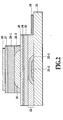
- Figure 2 is a structural drawing of an APD in accordance with a second embodiment of the present invention.
- an InP buffer layer 22 On an n-type InP electrode layer 21, an InP buffer layer 22, an InP avalanche multiplication layer 23, an InP electric field control layer 24, and an InGaAsP bandgap graded layer 25 are sequentially formed.
- an optical absorption layer and others which make up a mesa structure are formed on the InGaAsP bandgap graded layer 25.
- What is characteristic of the present invention is the provision of a second optical absorption layer.
- a low-concentration second InGaAs optical absorption layer 26-2 which is depleted in an operating state, is firstly formed.
- a first p-type InGaAs optical absorption layer 26-1, a p-type InGaAsP electrode layer 27, and a metal electrode 29 are provided.
- a metal electrode 29 is also provided.
- n-type InP doping regions 22-1 and 22-2 are formed in a part of the InP buffer layer 22, n-type InP doping regions 22-1 and 22-2 are formed.
- the n-type InP doping region 22-2 is included in the n-type InP doping region 22-1, and the n-type InP doping regions 22-1 and 22-2 have different doping concentrations.
- the periphery of the n-type InP doping region 22-1 is arranged to be located inside of the periphery of the mesa structure of the first p-type InGaAs optical absorption layer 26-1. Such an arrangement is also the same as described in the first embodiment.
- An APD having this structure can be produced according to the same method as described in the first embodiment.
- n-type InP doping regions 22-1 and 22-2 are formed inside the periphery of the mesa structure region in the view from the direction perpendicular to the lamination planes of the APD; thus, a depleted region 30 is generated within the second InGaAs optical absorption layer 26-2.
- simply thickening the InP buffer layer 22 to a reasonable degree is also effective in preventing depletion of the lateral side of the optical absorption layer, and in preventing electric field generation in an avalanche multiplication layer.
- thickening is not as effective as introduction of the guard ring structure described in the first embodiment, it is certainly effective in preventing depletion.
- the second embodiment is, together with the guard ring structure of the first embodiment, characterized by including two optical absorption layers.
- the second embodiment is characterized by further including a low-concentration second InGaAs optical absorption layer 26-2 being added between the first p-type InGaAs optical absorption layer 26-1 and the InP avalanche multiplication layer 23 in the conventional structure. Since the thickness of the whole optical absorption layer in this structure is increased, responsivity of the optical absorption layer can be improved without lowering the operation band width. This is also described in detail in Japanese Patent Application Laid-open No. 2005-223022 (patent document 2) by the inventors of the present application.
- the guard ring structure shown in the first embodiment namely "electric field concentration relaxation structure”
- thickness of the second InGaAs optical absorption layer 26-2 is set as large as possible within the range in which no breakdown occurs.
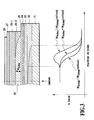
- FIG. 3 is a schematic drawing showing how an avalanche multiplication coefficient M changes in the device when thickness of the low-doping concentration second InGaAs optical absorption layer 26-2 is changed.
- W Adep is thicker than a threshold value W Adep (critical)
- the avalanche multiplication coefficient M value from the center point of the mesa structure of the device towards the peripheral region thereof, once increases and then decreases. That means edge breakdown occurs.
- W Adep is thicker than a threshold value W Adep (critical)
- the avalanche multiplication coefficient M value increases as a result.
- W Adep(critical) is calculated to be approximately 4000A when the concentration of the n-type InP doping region 22 is set to be 2 ⁇ 10 17 /cm 3 . It is certain that W Adep (critical) changes according to W AV . As thicker the W AV , larger W Adep (critical) becomes.
- the electron-injection type APD has been expected to demonstrate superior performance in principle, compared to the hole-injection type ADP including a conventional InP avalanche multiplication layer, a high production technology is required to obtain a stable and highly-reliable device. There is also a problem to be solved in terms of cost.
- the present invention which utilizes a relatively easy production technology, such as ion implantation, upon introducing a "guard ring structure," it is possible to produce an electron-injection type APD in which no edge breakdown occurs and light-receiving efficiency can be maximized. Requiring no diffusion technique, the present invention not only has an advantage in terms of production cost, but also enables to provide an APD device applicable to the next generation 40Gb/s system.
- the edge electric field in the peripheral part of the avalanche multiplication region can be relaxed without adopting of a diffusion technique, it is possible to produce an electron-injection type APD with low dark current in a highly controlled manner.
Landscapes
- Light Receiving Elements (AREA)
Abstract
Description
- The present invention relates to an ultrafast avalanche photodiode operating at the long-wavelength used for optical communication, and, more particularly, the present invention relates a guard ring structure for securing a stable operation of an avalanche photodiode capable of ultrafast operation.
- In response to the internet and multimedia being in widespread use in recent years, a high-speed, high-capacity optical communications system is demanded. Under the circumstances with such a demand, a system with a transmission rate of 40Gbit/s has been expected to be implemented on the basis of a faster channel transmission rate and multichannel WDM. In an optical communications system, one of the most important parts exerting an influence on the system performance is an avalanche photodiode which converts an optical signal to an electrical signal. The avalanche photodiode (hereafter referred to as APD) is a device utilized as a low-noise optical receiver, which generates carriers (electron and hole) by optical absorption, multiplies the carrier by an avalanche mechanism, and extract the output electrical signal from the carrier current.
- An APD operating at the long-wavelength has already been introduced widely to 2.5Gbit/s and 10Gbit/s systems, and a device which is applicable to the next-generation system with the rate of 40Gbit/s is in process of being developed. A hole-injection type APD having an InP avalanche multiplication layer has been commonly adopted as a relatively low-speed APD structure. Recently, an electron-injection type APD, which is superior in terms of operation speed, has been attracting attention.
- A long-wavelength APD having an InGaAs optical absorption layer commonly employs an SAM (Separated Absorption and Multiplication) structure, in which an optical absorption layer and an avalanche multiplication layer (avalanche layer) are separated to suppress an increase of dark current induced by a narrow gap semiconductor. For control of the electric field intensity of the optical absorption layer and of the electric field intensity of the avalanche multiplication layer independently, an electric-field control layer and a bandgap graded layer are provided between the optical absorption layer and the avalanche multiplication layer.
-
Figure 4 is a cross-sectional view showing a conventional mesa-type APD. The electron-injection type APD shown inFigure 4 is configured to have anoptical absorption layer 46 composed of a depleted InGaAs and anavalanche multiplication layer 43 composed of either InAlAs or InP. To be more specific, an electric-field control layer 44 and a bandgap gradedlayer 45 are provided between theavalanche multiplication layer 43 and the InGaAsoptical absorption layer 46 which both are provided on an n-InP electrode layer 41. AnInGaAs electrode layer 47 is formed on theoptical absorption layer 46, and anelectrode 49 is further formed thereon. Anelectrode 48 is also provided on the n-InP electrode layer 41. Unlike the hole-injection type APD, a guard ring structure which is formed by using a Zn diffusion technique cannot be adopted; therefore, a typical electron-injection type ADP is only allowed to have a mesa-type device structure as shown inFigure 4 . As a result, a fundamental problem arises in which dark current is increased around the junction periphery of the device. - In order to solve such a problem with dark current, various proposals have been made. For example, a structure in which an InP regrown layer covers the area around the mesa structure of a device has been proposed (refer to nonpatent document 1), and good characteristics have been reported. A structure in which electric field distribution is modulated around the operation region by ion implantation has also been reported (nonpatent document 2). Furthermore, a structure is also proposed in which a buffer layer including an n-type doped partial in-plane region is inserted between an avalanche multiplication layer and an n electrode layer so that the electric field intensity around the mesa becomes lower than that of the inside in operation (patent document 1).
- However, even the proposed techniques described above have the following problems still remained to be solved. In the technique proposed in the nonpatent document 1, implanting a mesa structure of a semiconductor by regrowth is generally difficult, since growth behavior varies according to plane index. The technique also has a disadvantage in terms of production cost. The structure proposed in the
nonpatent document 2, in which electric field distribution is modulated around the operation region by ion implantation, creates a trap level due to damage caused by implanted ion. Since impurities are non-activated by the trap level, there is a persisting concern about stability of the device. Regarding the structure proposed in the patent document 1, no practical guidance has been disclosed yet for designing the buffer layer including the n-type doped partial region. - As described above, although it is expected that the electron-injection type APD demonstrates superior features to those of the conventional hole-injection type APD, there were problems in terms of an increase of dark current and securing the device life time. A structure has also been proposed in which a mesa is buried in APD by use of semiconductor; however, the problems in difficulty of the production technique and production cost still remain to be solved. Having been made in consideration of the above-described problems, the present invention aims to provide a production technique of an electron-injection type APD without using of a diffusion technique. In addition, the provide APD has to be capable of providing a stable operation with low dark current. A technique regarding a "guard ring structure" is applied to the present invention for the purpose of achieving stable operation of the electron-injection type APD. Detailed explanations will be provided in the following section.
-
- Patent document 1:
Japanese Patent Application Laid-open No. 2005-086109 - Patent document 2:
Japanese Patent Application Laid-open No. 2005-223022 - Nonpatent document 1: S. Tanaka, S. Fujisaki, Y. Matsuoka, T. Tsuchiya, S. Tsuji, "10Gbit/s Avalanche Photodiodes Applicable to Non-Hermetic Receiver Modules, " OFC2003, Vol. 1, MF55, p67
- Nonpatent document 2: Shono, Endo, Inomoto, Watanabe, Makita, Nakata, "10Gbit/s high-sensitivity planar type APD for small optical receiver module" 2004 Proceedings of the Institute of Electronics, Information, and Communication Engineers General Conference C-4-37, p365
- In order to achieve the above-described goals, the invention described in claim 1 provides an avalanche photodiode. The avalanche photodiode is formed by sequentially laminating an n-type electrode layer, an avalanche multiplication layer, an electric field control layer, and a bandgap graded layer. On the bandgap graded layer, an optical absorption layer forming a mesa structure and a p-type electrode layer are sequentially formed. The avalanche photodiode is characterized by having a buffer layer and an n-type doping region. The buffer layer is formed between the n-type electrode layer and the avalanche multiplication layer. The n-type doping region having a substantially trapezoidal cross section area perpendicular to the laminated plane is formed on the inside of the interior portion of a region included in the interior portion of the buffer layer, having a contact with the n-type electrode layer, and having the mesa structure formed therein within the laminated plane. When the two nodes between the p-type electrode layer and the n-type electrode layer are reversely biased, the vicinity portion of the upper hem in the substantially trapezoidal cross section area in the n-type doping region is approximately depleted.
- The invention described in
claim 2 is characterized in that the n-type doping region has concentration distributions monotonically increasing from the avalanche multiplication layer towards the n-type electrode layer and from the peripheral region towards the center within the n-type doping region. - The invention described in claim 3 is characterized by having a first p-type optical absorption layer which is formed underneath a p-type electrode, and a low-concentration second optical absorption layer which is formed between the first optical absorption layer and the bandgap graded layer, and is depleted when the p-type electrode layer and the n-type electrode layer are reversely biased.
- The invention described in claim 4 is characterized in that the second optical absorption layer has a thickness set to be the maximum thickness fulfilling the condition in which in-plane distribution of avalanche multiplication coefficient in the device monotonically decreases from the center to the peripheral direction within the n-type doping region.
- The invention described in claim 5 is characterized in that each of the avalanche multiplication layer, the optical absorption layer, the first optical absorption layer, and the second optical absorption layer is composed of an InP/InGaAsP-based compound semiconductor or an InAIGaAs-based compound semiconductor.
- According to the present invention, it is possible to relax the edge electric field in the peripheral part of the avalanche multiplication region without using a diffusion technique, and therefore possible to produce an electron-injection type APD with low dark current in a highly controlled manner.
-
- [
Fig. 1] Figure 1 is a cross-sectional view of the structure of an APD in accordance with a first embodiment of the present invention, - [
Fig. 2] Figure 2 is a cross-sectional view of the structure of an APD in accordance with a second embodiment of the present invention, - [
Fig. 3] Figure 3 shows a positional change of M with the thickness of a low-doping optical absorption layer as a parameter. - [
Fig. 4] Figure 4 is a cross-sectional view of the structure of a conventional mesa-type APD, and - [
Fig. 5] Figure 5 shows electric field concentration in the buffer layer. -
Figure 1 is a structural drawing of an APD in accordance with a first embodiment of the present invention. On an n-typeInP electrode layer 11, anInP buffer layer 12, an InPavalanche multiplication layer 13, an InP electricfield control layer 14, and an InGaAsP bandgap gradedlayer 15 are formed in order. Furthermore, on the InGaAsP bandgap gradedlayer 15, a p-type InGaAsoptical absorption layer 16 in a mesa structure, a p-typeInGaAsP electrode layer 17, and a metal electrode 18 are provided. On the n-typeInP electrode layer 11, ametal electrode 19 is also provided. - In addition, n-type InP doping regions 12-1 and 12-2 are formed locally within the
InP buffer layer 12. The n-type InP doping region 12-2 is included within the n-type InP doping region 12-1. Furthermore, the n-type InP doping regions 12-1 and 12-2 have different doping concentrations. The structure and the fabrication method will be explained in detail in the later section. As will hereinafter be explained, with allocation of the n-type InP doping regions 12-1 and 12-2, an APD structure is obtained in which the surrounding region of the n-type InP doping regions 12-1 and 12-2 functions as a "guard ring." - In the present invention, it is an important point that the n-type InP doping region 12-1 is arranged so that the n-type InP doping region 12-1 is located inside of the periphery of the mesa structure of the InGaAs
optical absorption layer 16. In the case of looking at the structure from the top ofFigure 1 (from top down inFigure 1 ), which shows a cross-sectional structure of the device, in other words, in the case of looking at the structure from a direction perpendicular to the laminated planes of the layers of the device, the n-type InP doping region 12-1 is approximately a circular form or an oval figure. The type InP doping region 12-1 is arranged so that the periphery of the n-type InP doping region 12-1 is located within an area of the mesa-structure defined by the InGaAsoptical absorption layer 16. In this structure, within the InPavalanche multiplication region 13 the electric field intensity in the part which has no n-type InP doping region 12-1 being located immediately below is decreased with a certain level of voltage applied; thus, depletion of the mesa lateral side of the InGaAsoptical absorption layer 16 is prevented. As a result, electric field generation can be prevented. When electric field generation is prevented, it is possible to significantly reduce dark current originating from the lateral side surface of the mesa structure, and therefore to contribute to enhance the reliability of the device. - The APD of the present invention provided with the guard ring structure including the n-type InP doping region 12-1 can be produced, for example, in the following manner. Firstly, in order to form an
InP buffer layer 12, an n-InP layer which corresponds to the n-typeInP electrode layer 11 is grown on an InP substrate, and then undoped InP crystals are grown to form an undoped InP layer on the n-InP layer. After the formation of thebuffer layer 12, the n-type InP doping regions 12-1 and 12-2 are formed by Si ion implantation. After implanted ion is activated in heat treatment, other layers, including layers from the InPavalanche multiplication layer 13 to the p-typeInGaAsP electrode layer 17, are also sequentially formed and grown thereon. The structures of the InGaAsoptical absorption layer 16 and theavalanche multiplication layer 13 are defined by mesa process. Lastly, themetal electrodes 18 and 19, which are ohmic electrodes, are deposited, and heat treatment is applied. - When a reversely biased voltage is applied to the metal electrode 18 and the
metal electrode 19, a high electric field is generated in the InPavalanche multiplication layer 13. The InP electricfield control layer 14 carries out a function to adjust the difference of electric fields between the bandgap gradedlayer 15 and the part adjacent to the bandgap gradedlayer 15 within the InGaAsoptical absorption layer 16 to a predetermined value. A part of the InPavalanche multiplication layer 13, that is, the part above the n-type InP doping regions 12-1 and 12-2, has a depleted layer which is thinner than the surrounding part, and therefore becomes an avalanche multiplier active region (high electric field region). - The n-type doping region 12-1 can be seen as a substantially trapezoidal form with a round portion around the upper hem in the cross-sectional surface perpendicular to the laminated planes of the APD layers, as shown in
Figure 1 . However, when a convex-trapezoidal n-type doping region 12-1 is introduced, local electric field concentration is prone to be generated in the part located on the side of InPavalanche multiplication layer 13. -
Figure 5 shows electric field concentration when a buried n-type InP region is provided in the buffer layer. The basic structure of the APD shown inFigure 5 is the same as that shown inFigure 1 . Difference betweenFigures 1 and5 is that the structure shown inFigure 5 is provided with the buried n-type InP region 52-1 in thebuffer layer 52. In this case, local electric field concentration indicated by the arrows is generated in the surrounding part of the buried n-type InP region 52-1 in the side of theavalanche multiplication layer 53. - Even in the doping region structure of the present invention, it can be sometimes difficult to implement an intended APD operation due to such electric field concentration. Therefore, the present invention has the following characteristics. Specifically, the n-type InP doping region 12-1 has doping concentration distribution. In addition, in the surrounding part of the n-
type doping region 12, the depleted region penetrates sufficiently deeply into the inside of the n-type InP doping region 12-1. A potential drop is generated in the part which the depleted region penetrates into. The potential drop can prevent an electric field increase in the upper side, that is, in the side of the InPavalanche multiplication layer 13, of the part in which the potential drop is generated; thus, it is possible to relax "electric field concentration at an edge part," which causes so-called local breakdown (edge breakdown). InFigure 1 , two n-type InP doping regions 12-1 and 12-2 are shown in order to indicate that there are different doping concentrations inside a doping region. It should, however, be noted that these 2 doping regions do not necessarily indicate that there were discontinuously differences in the characteristics of the two regions thus formed. - Hence, in order to prevent local breakdown (edge breakdown) more effectively, it is only necessary to set monotonically increasing doping profiles of the n-type InP doping region 12-1 each from the side of the
avalanche multiplication layer 13 toward the n-type electrode layer 11, and from the peripheral region toward the center within the n-type InP doping region 12-1. Such a doping profile is so-called graded concentration distribution. Graded concentration distribution can be formed by utilizing spread of implanted ions in the depth direction and in the lateral direction. Thus, when the projection length of implanted ions is set to be in the vicinity of the interface between the n-typeInP electrode layer 11 layer and theInP buffer layer 12 layer, electric field change in the lateral direction can be moderate. Hence, local concentration of electric fields is confined within the n-type doping region 12-1, and therefore local breakdown can be effectively prevented. Without employing a diffusion technique, the present invention can implement an intended APD operation by ion implantation which is relatively easy. - As described above, it is possible to relax an edge electric field in the surrounding area of the avalanche multiplication region by adopting the guard ring structure, which is characteristic of the present invention. Hence, an electron-injection type APD with low dark current can be produced in a highly controlled manner.
-
Figure 2 is a structural drawing of an APD in accordance with a second embodiment of the present invention. On an n-typeInP electrode layer 21, anInP buffer layer 22, an InPavalanche multiplication layer 23, an InP electricfield control layer 24, and an InGaAsP bandgap gradedlayer 25 are sequentially formed. Furthermore, on the InGaAsP bandgap gradedlayer 25, an optical absorption layer and others which make up a mesa structure are formed. What is characteristic of the present invention is the provision of a second optical absorption layer. - To be more specific, on the InGaAsP bandgap graded
layer 25, a low-concentration second InGaAs optical absorption layer 26-2, which is depleted in an operating state, is firstly formed. On the top of this, as described in the first embodiment, a first p-type InGaAs optical absorption layer 26-1, a p-typeInGaAsP electrode layer 27, and ametal electrode 29 are provided. On the top of the n-typeInP electrode layer 21, ametal electrode 29 is also provided. - As described in the first embodiment, in a part of the
InP buffer layer 22, n-type InP doping regions 22-1 and 22-2 are formed. The n-type InP doping region 22-2 is included in the n-type InP doping region 22-1, and the n-type InP doping regions 22-1 and 22-2 have different doping concentrations. The periphery of the n-type InP doping region 22-1 is arranged to be located inside of the periphery of the mesa structure of the first p-type InGaAs optical absorption layer 26-1. Such an arrangement is also the same as described in the first embodiment. An APD having this structure can be produced according to the same method as described in the first embodiment. The n-type InP doping regions 22-1 and 22-2 are formed inside the periphery of the mesa structure region in the view from the direction perpendicular to the lamination planes of the APD; thus, a depletedregion 30 is generated within the second InGaAs optical absorption layer 26-2. - In general, simply thickening the
InP buffer layer 22 to a reasonable degree is also effective in preventing depletion of the lateral side of the optical absorption layer, and in preventing electric field generation in an avalanche multiplication layer. Although such thickening is not as effective as introduction of the guard ring structure described in the first embodiment, it is certainly effective in preventing depletion. - The second embodiment is, together with the guard ring structure of the first embodiment, characterized by including two optical absorption layers. In other words,-the second embodiment is characterized by further including a low-concentration second InGaAs optical absorption layer 26-2 being added between the first p-type InGaAs optical absorption layer 26-1 and the InP
avalanche multiplication layer 23 in the conventional structure. Since the thickness of the whole optical absorption layer in this structure is increased, responsivity of the optical absorption layer can be improved without lowering the operation band width. This is also described in detail inJapanese Patent Application Laid-open No. 2005-223022 - Even if the guard ring structure shown in the first embodiment, namely "electric field concentration relaxation structure," is introduced, it is not always possible to avoid edge breakdown for the low-concentration second InGaAs optical absorption layer 26-2 with a given thickness. In the present invention, thickness of the second InGaAs optical absorption layer 26-2 is set as large as possible within the range in which no breakdown occurs. Next, a method for determining thickness of the second InGaAs optical absorption layer will be explained.
-
Figure 3 is a schematic drawing showing how an avalanche multiplication coefficient M changes in the device when thickness of the low-doping concentration second InGaAs optical absorption layer 26-2 is changed. When WAdep is thicker than a threshold value WAdep(critical), the avalanche multiplication coefficient M value, from the center point of the mesa structure of the device towards the peripheral region thereof, once increases and then decreases. That means edge breakdown occurs. Under such a condition, even if the electric field of the InPavalanche multiplication layer 23 is decreased, and an ionization rate is accordingly decreased, the effect by spread of thickness of the effective avalanche multiplication layer becomes more dominant. Thus, the avalanche multiplication coefficient M value increases as a result. - Hence, it is possible to avoid edge breakdown by setting the thickness of the low-concentration second InGaAs optical absorption layer 26-2 to the maximum thickness which allows the avalanche multiplication coefficient M to decrease monotonically from the center point of the mesa structure to the peripheral part thereof.
For an APD structure including a typical InP avalanche multiplication layer with the thickness of WAV=2500A, WAdep(critical) is calculated to be approximately 4000A when the concentration of the n-typeInP doping region 22 is set to be 2×10¹⁷/cm3. It is certain that WAdep(critical) changes according to WAV. As thicker the WAV, larger WAdep(critical) becomes. - As described in detail above, although the electron-injection type APD has been expected to demonstrate superior performance in principle, compared to the hole-injection type ADP including a conventional InP avalanche multiplication layer, a high production technology is required to obtain a stable and highly-reliable device. There is also a problem to be solved in terms of cost. According to the present invention which utilizes a relatively easy production technology, such as ion implantation, upon introducing a "guard ring structure," it is possible to produce an electron-injection type APD in which no edge breakdown occurs and light-receiving efficiency can be maximized. Requiring no diffusion technique, the present invention not only has an advantage in terms of production cost, but also enables to provide an APD device applicable to the next generation 40Gb/s system.
- According to the present invention, in which the edge electric field in the peripheral part of the avalanche multiplication region can be relaxed without adopting of a diffusion technique, it is possible to produce an electron-injection type APD with low dark current in a highly controlled manner.
Claims (5)
- An avalanche photodiode formed by sequentially depositing an n-type electrode layer, an avalanche multiplication layer, an electric field control layer, a bandgap graded layer, an optical absorption layer and a p-type electrode layer, the optical absorption layer and the p-type electrode layer forming a mesa structure, the avalanche photodiode comprising:a buffer layer formed between the n-type electrode layer and the avalanche multiplication layer; andan n-type doping region being formed inside of said buffer layer and within an area defined by said mesa structure, as viewed from the mesa structure, being brought into contact with the n-type electrode layer, having a substantially trapezoidal shape in cross section, and being approximately depleted in the vicinity of the upper hem thereof when the p-type electrode layer and the n-type electrode layer are reversely biased.
- The avalanche photodiode according to claim 1, wherein the n-type doping region has a monotonically increasing concentration distribution both from the avalanche multiplication layer toward the n-type electrode layer and from the peripheral region towards the center within the n-type doping region.
- The avalanche photodiode according to any of claims 1 and 2, wherein said optical absorption layer includes:a first p-type optical absorption layer being formed underneath the p-type electrode layer; anda low-concentrated second optical absorption layer being formed between the first optical absorption layer and the bandgap graded layer, and being depleted when the p-type electrode layer and the n-type electrode layer are reversely biased.
- The avalanche photodiode according to any of claims 1 to 3, wherein the second optical absorption layer has a thickness that is set to be the maximum thickness fulfilling the condition in which the in-plane distribution of avalanche multiplication coefficient in the device monotonically decreases from the center to the peripheral direction within the n-type doping region.
- The avalanche photodiode according to any of the claims 1 to 4, wherein each of the avalanche multiplication layer, the optical absorption layer, the first optical absorption layer, and the second optical absorption layer is composed of any one of an InP/InGaAsP-based compound semiconductor and an InAlGaAs-based compound semiconductor.
Applications Claiming Priority (2)
| Application Number | Priority Date | Filing Date | Title |
|---|---|---|---|
| JP2005186551A JP4234116B2 (en) | 2005-06-27 | 2005-06-27 | Avalanche photodiode |
| PCT/JP2006/312800 WO2007000996A1 (en) | 2005-06-27 | 2006-06-27 | Avalanche photodiode |
Publications (3)
| Publication Number | Publication Date |
|---|---|
| EP1898472A1 true EP1898472A1 (en) | 2008-03-12 |
| EP1898472A4 EP1898472A4 (en) | 2008-06-25 |
| EP1898472B1 EP1898472B1 (en) | 2010-10-06 |
Family
ID=37595245
Family Applications (1)
| Application Number | Title | Priority Date | Filing Date |
|---|---|---|---|
| EP06767417A Ceased EP1898472B1 (en) | 2005-06-27 | 2006-06-27 | Avalanche photodiode |
Country Status (5)
| Country | Link |
|---|---|
| US (1) | US7880197B2 (en) |
| EP (1) | EP1898472B1 (en) |
| JP (1) | JP4234116B2 (en) |
| DE (1) | DE602006017371D1 (en) |
| WO (1) | WO2007000996A1 (en) |
Families Citing this family (24)
| Publication number | Priority date | Publication date | Assignee | Title |
|---|---|---|---|---|
| JP2010135360A (en) * | 2008-12-02 | 2010-06-17 | Mitsubishi Electric Corp | Avalanche photodiode |
| JP4728386B2 (en) * | 2008-12-17 | 2011-07-20 | Nttエレクトロニクス株式会社 | Avalanche photodiode |
| JP5091886B2 (en) | 2009-02-13 | 2012-12-05 | 浜松ホトニクス株式会社 | Image sensor |
| JP5271104B2 (en) | 2009-02-13 | 2013-08-21 | 浜松ホトニクス株式会社 | Linear image sensor |
| JP5357793B2 (en) * | 2010-01-29 | 2013-12-04 | 日本放送協会 | Photoconductive target and imaging tube and imaging device using the same |
| JP5327892B2 (en) | 2010-09-02 | 2013-10-30 | Nttエレクトロニクス株式会社 | Avalanche photodiode |
| JP5631668B2 (en) | 2010-09-02 | 2014-11-26 | Nttエレクトロニクス株式会社 | Avalanche photodiode |
| US8816461B2 (en) * | 2011-09-13 | 2014-08-26 | The Boeing Company | Dichromatic photodiodes |
| US9160949B2 (en) * | 2013-04-01 | 2015-10-13 | Omnivision Technologies, Inc. | Enhanced photon detection device with biased deep trench isolation |
| JP2015211166A (en) * | 2014-04-28 | 2015-11-24 | 日本電信電話株式会社 | Semiconductor light-receiving element and method for manufacturing the same |
| US10032950B2 (en) | 2016-02-22 | 2018-07-24 | University Of Virginia Patent Foundation | AllnAsSb avalanche photodiode and related method thereof |
| US9466751B1 (en) * | 2016-03-04 | 2016-10-11 | National Central University | Avalanche photodiode having electric-field confinement by mesas |
| JP6705762B2 (en) * | 2017-03-14 | 2020-06-03 | 日本電信電話株式会社 | Avalanche photodiode |
| CN106887469B (en) * | 2017-03-22 | 2019-05-07 | 武汉光谷量子技术有限公司 | Epitaxial structure of avalanche diode and manufacturing method of avalanche diode |
| CN107749424B (en) * | 2017-10-24 | 2023-11-07 | 江门市奥伦德光电有限公司 | An avalanche photodiode and its preparation method |
| US11101400B2 (en) * | 2017-11-28 | 2021-08-24 | Luxtera Llc | Method and system for a focused field avalanche photodiode |
| JP7081551B2 (en) * | 2019-03-28 | 2022-06-07 | 日本電信電話株式会社 | Avalanche photodiode and its manufacturing method |
| TWI851794B (en) | 2019-08-22 | 2024-08-11 | 美商光程研創股份有限公司 | Photo-current amplification apparatus and method for operating photodetecting device |
| CN112447875B (en) * | 2019-08-30 | 2024-03-08 | 光程研创(美商)股份有限公司 | Avalanche photoelectric crystal element and its light detection method |
| CN110690314B (en) * | 2019-09-05 | 2023-06-27 | 中国电子科技集团公司第十三研究所 | Ultraviolet detector with absorption layer and multiplication layer in separate structures and preparation method thereof |
| WO2021100082A1 (en) | 2019-11-18 | 2021-05-27 | 日本電信電話株式会社 | Light receiving element and method for producing same |
| US11056604B1 (en) * | 2020-02-18 | 2021-07-06 | National Central University | Photodiode of avalanche breakdown having mixed composite charge layer |
| CA3191020A1 (en) * | 2020-08-28 | 2022-03-03 | National Research Council Of Canada | Mesa avalanche photodiode with sidewall passivation |
| CN119300487B (en) * | 2024-09-30 | 2025-09-23 | 浙江大学 | A Pocket-doped 4H-SiC-based avalanche photodiode device |
Family Cites Families (7)
| Publication number | Priority date | Publication date | Assignee | Title |
|---|---|---|---|---|
| JP2934294B2 (en) | 1990-04-09 | 1999-08-16 | 日本電信電話株式会社 | Avalanche photodiode |
| JP2845081B2 (en) | 1993-04-07 | 1999-01-13 | 日本電気株式会社 | Semiconductor light receiving element |
| JP2601231B2 (en) | 1994-12-22 | 1997-04-16 | 日本電気株式会社 | Superlattice avalanche photodiode |
| JPH11330536A (en) * | 1998-05-13 | 1999-11-30 | Nec Corp | Semiconductor light receiving element |
| JP3141847B2 (en) * | 1998-07-03 | 2001-03-07 | 日本電気株式会社 | Avalanche photodiode |
| JP4191564B2 (en) | 2003-09-10 | 2008-12-03 | Nttエレクトロニクス株式会社 | Avalanche photodiode |
| JP2005223022A (en) | 2004-02-03 | 2005-08-18 | Ntt Electornics Corp | Avalanche photodiode |
-
2005
- 2005-06-27 JP JP2005186551A patent/JP4234116B2/en not_active Expired - Fee Related
-
2006
- 2006-06-27 US US11/993,801 patent/US7880197B2/en active Active
- 2006-06-27 EP EP06767417A patent/EP1898472B1/en not_active Ceased
- 2006-06-27 WO PCT/JP2006/312800 patent/WO2007000996A1/en not_active Ceased
- 2006-06-27 DE DE602006017371T patent/DE602006017371D1/en active Active
Also Published As
| Publication number | Publication date |
|---|---|
| US7880197B2 (en) | 2011-02-01 |
| DE602006017371D1 (en) | 2010-11-18 |
| WO2007000996A1 (en) | 2007-01-04 |
| US20100163925A1 (en) | 2010-07-01 |
| JP2007005697A (en) | 2007-01-11 |
| JP4234116B2 (en) | 2009-03-04 |
| EP1898472A4 (en) | 2008-06-25 |
| EP1898472B1 (en) | 2010-10-06 |
Similar Documents
| Publication | Publication Date | Title |
|---|---|---|
| EP1898472B1 (en) | Avalanche photodiode | |
| EP1811578B1 (en) | Avalanche photodiode | |
| US8575650B2 (en) | Avalanche photodiode | |
| US7345325B2 (en) | Avalanche photodiode | |
| EP2613366B1 (en) | Avalanche photodiode | |
| US7855400B2 (en) | Semiconductor light detecting element and method for manufacturing the semiconductor light detecting element | |
| JP2010135360A (en) | Avalanche photodiode | |
| EP2613365B1 (en) | Avalanche photodiode | |
| JP5015494B2 (en) | Semiconductor photo detector | |
| US20240154053A1 (en) | Ge on si photodetector with gain | |
| JP2005223022A (en) | Avalanche photodiode | |
| JP2008028421A (en) | Avalanche photodiode | |
| JP2002231992A (en) | Semiconductor light receiving element | |
| JP5303793B2 (en) | Photodiode | |
| JPS6285477A (en) | Optical semiconductor device | |
| JPS6358382B2 (en) | ||
| JP4191564B2 (en) | Avalanche photodiode | |
| US20260090114A1 (en) | Back-illuminated light receiving device | |
| JP2763352B2 (en) | Semiconductor light receiving element | |
| JP2000068550A (en) | Pin type semiconductor light receiving element | |
| JPS61267375A (en) | Planar type hetero junction semiconductor photodetector | |
| HK1113520A1 (en) | Planar avalanche photodiode | |
| HK1113520B (en) | Planar avalanche photodiode |
Legal Events
| Date | Code | Title | Description |
|---|---|---|---|
| PUAI | Public reference made under article 153(3) epc to a published international application that has entered the european phase |
Free format text: ORIGINAL CODE: 0009012 |
|
| 17P | Request for examination filed |
Effective date: 20071227 |
|
| AK | Designated contracting states |
Kind code of ref document: A1 Designated state(s): DE FR GB |
|
| DAX | Request for extension of the european patent (deleted) | ||
| A4 | Supplementary search report drawn up and despatched |
Effective date: 20080528 |
|
| RBV | Designated contracting states (corrected) |
Designated state(s): DE FR GB |
|
| DAX | Request for extension of the european patent (deleted) | ||
| 17Q | First examination report despatched |
Effective date: 20080910 |
|
| GRAP | Despatch of communication of intention to grant a patent |
Free format text: ORIGINAL CODE: EPIDOSNIGR1 |
|
| GRAS | Grant fee paid |
Free format text: ORIGINAL CODE: EPIDOSNIGR3 |
|
| GRAA | (expected) grant |
Free format text: ORIGINAL CODE: 0009210 |
|
| AK | Designated contracting states |
Kind code of ref document: B1 Designated state(s): DE FR GB |
|
| REG | Reference to a national code |
Ref country code: GB Ref legal event code: FG4D |
|
| RAP2 | Party data changed (patent owner data changed or rights of a patent transferred) |
Owner name: NIPPON TELEGRAPH AND TELEPHONE CORPORATION Owner name: NTT ELECTRONICS CORPORATION |
|
| REF | Corresponds to: |
Ref document number: 602006017371 Country of ref document: DE Date of ref document: 20101118 Kind code of ref document: P |
|
| PLBE | No opposition filed within time limit |
Free format text: ORIGINAL CODE: 0009261 |
|
| STAA | Information on the status of an ep patent application or granted ep patent |
Free format text: STATUS: NO OPPOSITION FILED WITHIN TIME LIMIT |
|
| 26N | No opposition filed |
Effective date: 20110707 |
|
| REG | Reference to a national code |
Ref country code: DE Ref legal event code: R097 Ref document number: 602006017371 Country of ref document: DE Effective date: 20110707 |
|
| REG | Reference to a national code |
Ref country code: FR Ref legal event code: PLFP Year of fee payment: 11 |
|
| REG | Reference to a national code |
Ref country code: FR Ref legal event code: PLFP Year of fee payment: 12 |
|
| REG | Reference to a national code |
Ref country code: FR Ref legal event code: PLFP Year of fee payment: 13 |
|
| PGFP | Annual fee paid to national office [announced via postgrant information from national office to epo] |
Ref country code: DE Payment date: 20190612 Year of fee payment: 14 |
|
| PGFP | Annual fee paid to national office [announced via postgrant information from national office to epo] |
Ref country code: FR Payment date: 20190510 Year of fee payment: 14 |
|
| PGFP | Annual fee paid to national office [announced via postgrant information from national office to epo] |
Ref country code: GB Payment date: 20190626 Year of fee payment: 14 |
|
| REG | Reference to a national code |
Ref country code: DE Ref legal event code: R119 Ref document number: 602006017371 Country of ref document: DE |
|
| GBPC | Gb: european patent ceased through non-payment of renewal fee |
Effective date: 20200627 |
|
| PG25 | Lapsed in a contracting state [announced via postgrant information from national office to epo] |
Ref country code: GB Free format text: LAPSE BECAUSE OF NON-PAYMENT OF DUE FEES Effective date: 20200627 Ref country code: FR Free format text: LAPSE BECAUSE OF NON-PAYMENT OF DUE FEES Effective date: 20200630 |
|
| PG25 | Lapsed in a contracting state [announced via postgrant information from national office to epo] |
Ref country code: DE Free format text: LAPSE BECAUSE OF NON-PAYMENT OF DUE FEES Effective date: 20210101 |