EP1897965B1 - A process for eliminating precipitates from a semiconductor II-VI material by annealing. - Google Patents
A process for eliminating precipitates from a semiconductor II-VI material by annealing. Download PDFInfo
- Publication number
- EP1897965B1 EP1897965B1 EP07115691A EP07115691A EP1897965B1 EP 1897965 B1 EP1897965 B1 EP 1897965B1 EP 07115691 A EP07115691 A EP 07115691A EP 07115691 A EP07115691 A EP 07115691A EP 1897965 B1 EP1897965 B1 EP 1897965B1
- Authority
- EP
- European Patent Office
- Prior art keywords
- temperature
- precipitates
- semiconductor material
- solid
- annealing
- Prior art date
- Legal status (The legal status is an assumption and is not a legal conclusion. Google has not performed a legal analysis and makes no representation as to the accuracy of the status listed.)
- Active
Links
- 239000000463 material Substances 0.000 title claims abstract description 81
- 239000002244 precipitate Substances 0.000 title claims abstract description 51
- 239000004065 semiconductor Substances 0.000 title claims abstract description 38
- 238000000034 method Methods 0.000 title claims description 64
- 238000000137 annealing Methods 0.000 title claims description 34
- 230000008569 process Effects 0.000 title description 24
- 239000007787 solid Substances 0.000 claims abstract description 29
- 238000000859 sublimation Methods 0.000 claims abstract description 28
- 230000008022 sublimation Effects 0.000 claims abstract description 28
- 238000001816 cooling Methods 0.000 claims abstract description 13
- 230000005496 eutectics Effects 0.000 claims abstract description 3
- 239000011261 inert gas Substances 0.000 claims abstract 4
- 229910004613 CdTe Inorganic materials 0.000 claims description 32
- 239000007789 gas Substances 0.000 claims description 23
- 230000007935 neutral effect Effects 0.000 claims description 23
- PORWMNRCUJJQNO-UHFFFAOYSA-N tellurium atom Chemical compound [Te] PORWMNRCUJJQNO-UHFFFAOYSA-N 0.000 claims description 23
- 239000000758 substrate Substances 0.000 claims description 22
- 229910052714 tellurium Inorganic materials 0.000 claims description 20
- XKRFYHLGVUSROY-UHFFFAOYSA-N Argon Chemical compound [Ar] XKRFYHLGVUSROY-UHFFFAOYSA-N 0.000 claims description 13
- 229910007709 ZnTe Inorganic materials 0.000 claims description 13
- 230000008018 melting Effects 0.000 claims description 9
- 238000002844 melting Methods 0.000 claims description 9
- 239000011343 solid material Substances 0.000 claims description 9
- 229910052786 argon Inorganic materials 0.000 claims description 6
- 238000010587 phase diagram Methods 0.000 claims description 6
- 239000002904 solvent Substances 0.000 claims description 6
- 150000001875 compounds Chemical class 0.000 claims description 3
- 239000001307 helium Substances 0.000 claims description 2
- 229910052734 helium Inorganic materials 0.000 claims description 2
- SWQJXJOGLNCZEY-UHFFFAOYSA-N helium atom Chemical compound [He] SWQJXJOGLNCZEY-UHFFFAOYSA-N 0.000 claims description 2
- 238000010438 heat treatment Methods 0.000 abstract description 2
- 239000012071 phase Substances 0.000 description 15
- 229910004611 CdZnTe Inorganic materials 0.000 description 10
- 239000010453 quartz Substances 0.000 description 10
- VYPSYNLAJGMNEJ-UHFFFAOYSA-N silicon dioxide Inorganic materials O=[Si]=O VYPSYNLAJGMNEJ-UHFFFAOYSA-N 0.000 description 10
- 230000007547 defect Effects 0.000 description 8
- 239000000203 mixture Substances 0.000 description 8
- 229910052793 cadmium Inorganic materials 0.000 description 7
- 230000005540 biological transmission Effects 0.000 description 6
- 238000013459 approach Methods 0.000 description 5
- OKTJSMMVPCPJKN-UHFFFAOYSA-N Carbon Chemical compound [C] OKTJSMMVPCPJKN-UHFFFAOYSA-N 0.000 description 4
- PEDCQBHIVMGVHV-UHFFFAOYSA-N Glycerine Chemical compound OCC(O)CO PEDCQBHIVMGVHV-UHFFFAOYSA-N 0.000 description 4
- 238000010586 diagram Methods 0.000 description 4
- 229910002804 graphite Inorganic materials 0.000 description 4
- 239000010439 graphite Substances 0.000 description 4
- 238000004519 manufacturing process Methods 0.000 description 4
- 238000013507 mapping Methods 0.000 description 4
- OKKJLVBELUTLKV-UHFFFAOYSA-N Methanol Chemical compound OC OKKJLVBELUTLKV-UHFFFAOYSA-N 0.000 description 3
- 230000008901 benefit Effects 0.000 description 3
- BDOSMKKIYDKNTQ-UHFFFAOYSA-N cadmium atom Chemical compound [Cd] BDOSMKKIYDKNTQ-UHFFFAOYSA-N 0.000 description 3
- 230000008030 elimination Effects 0.000 description 3
- 238000003379 elimination reaction Methods 0.000 description 3
- 230000008020 evaporation Effects 0.000 description 3
- 238000001704 evaporation Methods 0.000 description 3
- 238000002188 infrared transmission spectroscopy Methods 0.000 description 3
- 230000003287 optical effect Effects 0.000 description 3
- 238000002360 preparation method Methods 0.000 description 3
- 239000013078 crystal Substances 0.000 description 2
- 238000002474 experimental method Methods 0.000 description 2
- 230000004927 fusion Effects 0.000 description 2
- 239000007791 liquid phase Substances 0.000 description 2
- 238000010926 purge Methods 0.000 description 2
- 238000000746 purification Methods 0.000 description 2
- XSOKHXFFCGXDJZ-UHFFFAOYSA-N telluride(2-) Chemical compound [Te-2] XSOKHXFFCGXDJZ-UHFFFAOYSA-N 0.000 description 2
- WKBOTKDWSSQWDR-UHFFFAOYSA-N Bromine atom Chemical compound [Br] WKBOTKDWSSQWDR-UHFFFAOYSA-N 0.000 description 1
- 241001080024 Telles Species 0.000 description 1
- 240000008042 Zea mays Species 0.000 description 1
- 230000009471 action Effects 0.000 description 1
- 125000004429 atom Chemical group 0.000 description 1
- GDTBXPJZTBHREO-UHFFFAOYSA-N bromine Substances BrBr GDTBXPJZTBHREO-UHFFFAOYSA-N 0.000 description 1
- 229910052794 bromium Inorganic materials 0.000 description 1
- 229910052799 carbon Inorganic materials 0.000 description 1
- 230000008859 change Effects 0.000 description 1
- 239000000470 constituent Substances 0.000 description 1
- 230000001419 dependent effect Effects 0.000 description 1
- 238000009826 distribution Methods 0.000 description 1
- 238000005188 flotation Methods 0.000 description 1
- 230000006872 improvement Effects 0.000 description 1
- 239000012535 impurity Substances 0.000 description 1
- 239000007788 liquid Substances 0.000 description 1
- 238000012423 maintenance Methods 0.000 description 1
- 239000011159 matrix material Substances 0.000 description 1
- 238000005259 measurement Methods 0.000 description 1
- 238000005272 metallurgy Methods 0.000 description 1
- 238000000386 microscopy Methods 0.000 description 1
- 238000012544 monitoring process Methods 0.000 description 1
- 238000005498 polishing Methods 0.000 description 1
- 238000001556 precipitation Methods 0.000 description 1
- 239000008247 solid mixture Substances 0.000 description 1
- 239000007858 starting material Substances 0.000 description 1
- 238000010408 sweeping Methods 0.000 description 1
- 239000012808 vapor phase Substances 0.000 description 1
- 229910052725 zinc Inorganic materials 0.000 description 1
Images


Classifications
-
- C—CHEMISTRY; METALLURGY
- C22—METALLURGY; FERROUS OR NON-FERROUS ALLOYS; TREATMENT OF ALLOYS OR NON-FERROUS METALS
- C22F—CHANGING THE PHYSICAL STRUCTURE OF NON-FERROUS METALS AND NON-FERROUS ALLOYS
- C22F1/00—Changing the physical structure of non-ferrous metals or alloys by heat treatment or by hot or cold working
- C22F1/16—Changing the physical structure of non-ferrous metals or alloys by heat treatment or by hot or cold working of other metals or alloys based thereon
-
- C—CHEMISTRY; METALLURGY
- C30—CRYSTAL GROWTH
- C30B—SINGLE-CRYSTAL GROWTH; UNIDIRECTIONAL SOLIDIFICATION OF EUTECTIC MATERIAL OR UNIDIRECTIONAL DEMIXING OF EUTECTOID MATERIAL; REFINING BY ZONE-MELTING OF MATERIAL; PRODUCTION OF A HOMOGENEOUS POLYCRYSTALLINE MATERIAL WITH DEFINED STRUCTURE; SINGLE CRYSTALS OR HOMOGENEOUS POLYCRYSTALLINE MATERIAL WITH DEFINED STRUCTURE; AFTER-TREATMENT OF SINGLE CRYSTALS OR A HOMOGENEOUS POLYCRYSTALLINE MATERIAL WITH DEFINED STRUCTURE; APPARATUS THEREFOR
- C30B29/00—Single crystals or homogeneous polycrystalline material with defined structure characterised by the material or by their shape
- C30B29/10—Inorganic compounds or compositions
- C30B29/46—Sulfur-, selenium- or tellurium-containing compounds
- C30B29/48—AIIBVI compounds wherein A is Zn, Cd or Hg, and B is S, Se or Te
-
- C—CHEMISTRY; METALLURGY
- C30—CRYSTAL GROWTH
- C30B—SINGLE-CRYSTAL GROWTH; UNIDIRECTIONAL SOLIDIFICATION OF EUTECTIC MATERIAL OR UNIDIRECTIONAL DEMIXING OF EUTECTOID MATERIAL; REFINING BY ZONE-MELTING OF MATERIAL; PRODUCTION OF A HOMOGENEOUS POLYCRYSTALLINE MATERIAL WITH DEFINED STRUCTURE; SINGLE CRYSTALS OR HOMOGENEOUS POLYCRYSTALLINE MATERIAL WITH DEFINED STRUCTURE; AFTER-TREATMENT OF SINGLE CRYSTALS OR A HOMOGENEOUS POLYCRYSTALLINE MATERIAL WITH DEFINED STRUCTURE; APPARATUS THEREFOR
- C30B33/00—After-treatment of single crystals or homogeneous polycrystalline material with defined structure
- C30B33/02—Heat treatment
Definitions
- the invention relates to a method for annealing the precipitates in a congruent sublimation semiconductor material II-VI, such as CdTe, CdZnTe or ZnTe.
- Said precipitates are generally constituted by one of the elements, namely element II, such as Cd or element VI, such as Te.
- the technical field of the invention can be defined as that of the preparation of semiconductor materials and their purification, that is to say the elimination of defects and impurities of these materials.
- tellurium precipitates of density and size dependent on the kinetics of cooling, are considered as potential sources of particularly troublesome defects during subsequent technological steps, such as the growth of epitaxial layers, the production of pn diodes, the manufacture of X and y detectors, and the manufacture of electro-optical components.
- the composition of this material can be adjusted to any value within the range of existence at that temperature.
- the stoichiometric composition line is included in the field of existence of the solid, the stoichiometric composition can be attained, as well as the solid compositions beyond the stoichiometric composition, in which case a change in the conductivity type is generally observed.
- the object of the present invention is to provide a method of annealing the precipitates in a semiconductor solid material II-VI, such as CdTe, CdZnTe or ZnTe, which meets, among others, these needs.
- ambient temperature is meant a temperature generally of 20 to 25 ° C for example 21 to 24 ° C, especially 22 to 23 ° C.
- the heating under the circulation of neutral gas and / or the maintenance under circulation of neutral gas and / or the cooling can be done without backpressure of element II and / or element VI. It is understood, however, that we use the terms "without" counterpressure there is in fact always some pressure elements II and / or VI inherent in sublimation. But no action is taken to establish a counterpressure as is the case in the prior art. The only pressure is that due naturally, in a way that is sublimated without doing anything for it.
- the process according to the invention does not present the difficulties, defects, limitations and disadvantages of the processes of the prior art and it solves the problems posed by the processes of the prior art, in particular the process according to the invention generally does not require unlike the methods of the prior art no pressure against element II or VI. As a result, the measures and regulations relating to the establishment of this counterpressure are eliminated.
- the method according to the invention is, among others, simple, reliable, easy to implement, reproducible and economical.
- the process according to the invention is distinguished in particular from the processes of the prior art such as those described in the documents US-A-5,201,985 , US-A-4,190,486 , US-A-4,481,044 , EP-A-0 423 463 , in that one operates under a neutral gas circulation.
- Such a circulation of neutral gas can be carried out with a tube, reactor, open-reactor in which the material is placed, generally in a crucible - as opposed to so-called “closed”, “sealed” tubes of the methods of the prior art. in which a circulation of neutral gas is, therefore, impossible.
- Operating under a neutral gas flow is totally different from operating in a simple atmosphere of neutral gas, stationary, without circulation, sweeping.
- the advantage of operating under a circulation of neutral gas is in particular to allow the entrainment of the vapors of elements II and VI such as tellurium and cadmium escaping, effusant, the material to be annealed for example by the orifice of a crucible operating in Knudsen cell.
- the circulation of neutral gas thus creates a situation of quasi-dynamic equilibrium above the material, for example in the dead volume of the crucible, motor, as it were, of the exit of the inclusions and precipitates, for example of element VI, such as tellurium initially present in the material, the sample to be annealed.
- the vapors thus entrained are condensed at the cold point of the reactor tube, as described below.
- the flow rate of neutral gas can be easily adapted by those skilled in the art, it can be for example from 10 to 1000 cc / minute, preferably from 100 to 500 cc / minute under a pressure of 1 atmosphere.
- the quasi-equilibrium situation can for example be schematized as described on the figure 5 .
- the quasi-equilibrium is auto-adaptive, especially during cooling, since the partial pressures of element VI and element II such as Cd and Te adapt themselves. same at the new temperature in order to respect the equilibrium constant.
- the phase equilibrium the elimination of precipitates which are thermodynamic defects.
- the first temperature T 1 is, in the phase diagram of the semiconductor material II-VI, the temperature corresponding to the intersection of the vertical passing through the maximum melting point of the material (this is the most important point). top of the solidus) and the solidus.
- the second temperature T 2 is, in the phase diagram of the semiconductor material II-VI, the temperature corresponding to the intersection of the congruent sublimation line and the solidus.
- the precipitates are generally precipitates of element VI.
- the semiconductor material II-VI is selected from CdTe, Cd 1-x Zn x Te where x is from 0 to 1, and ZnTe.
- This type of material generally contains as precipitates only tellurium precipitates.
- the material is CdTe, the precipitates consisting solely of tellurium, the first temperature T 1 is 830 ° C and the second temperature T 2 is 1040 ° C.
- the material is ZnTe, the precipitates consisting solely of tellurium, the first temperature T 1 is 820 ° C and the second temperature T 2 is 1240 ° C.
- the time during which the solid material is maintained at the temperature T constant is 1 minute to 50 hours.
- This holding time at the single temperature T, or annealing time depends on the volume of the material subjected to the process and the chosen temperature.
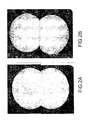
- a 5-minute annealing time is sufficient to purge the substrate of the second phase (ie Te precipitates). contained, as shown in the attached figures.
- the annealing is carried out at a single, constant temperature, with no temperature profile and complex temperature regulation.
- the semiconductor material II-VI treated by the process according to the invention can be in a large variety of forms, it can in particular be in the form of a single substrate or of several substrates, each of these substrates can be present in the form of a block or ingot.
- the neutral gas is generally selected from argon and helium.
- the semiconductor solid material II-VI may be a material produced by a BRIDGMAN method at the maximum melting point or as a solvent of element VI, such as Te.
- the material is placed in a crucible designed as a KNUDSEN cell.
- the process is carried out in a tube, reactor, open which allows a circulation, neutral gas sweep.
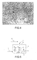
- the basic principle of the invention which is based essentially on the phase equilibrium diagram of the solid semiconductor material, is illustrated on the figure 1 .
- this ingot brought to a temperature between these two limits, is placed in an open tube in which a neutral gas circulates, such as Ar, without any backpressure of Cd or Te, then, whatever its initial deviation to stoichiometry, its composition will evolve, at a constant temperature, so as to be wedged on the line of congruent sublimation: in its field of existence, the solid does not contains no precipitate; it is then sufficient to cool this solid at a sufficiently slow rate so that at each moment it equilibrates with its vapor and is confused, during cooling, with the line of congruent sublimation.
- This line being included in the equilibrium domain, never crosses the solidus line and makes it possible to recover, at ambient temperature, a solid free of precipitates.
- the material II-VI such as CdTe may comprise inclusions (3) for example of element VI such as Te.
- element VI such as Te
- the material in the crucible is CdTe with inclusions of Te.
- the material constituting the crucible (1) is preferably easy to machine and must have a thermal conductivity favoring isothermicity, graphite, for example, may be perfectly suitable.
- the crucible is designed to receive the sample and to provide, above it, a dead volume (4) sufficient to ensure, during the annealing step, a pseudo-balance (represented by the double arrows 5) between the solid to be annealed and its vapor phase (PCd and PTe pressures); the crucible (1) is closed by a plug made of the same material as the body of the crucible; this plug carries a calibrated orifice (6) allowing the assembly to function as a KNUDSEN cell. It is through this orifice (6) that the most volatile element constituting material II-VI will evaporate primarily (arrow 7).
- the quartz tube containing crucible and sample is introduced into an oven and brought to the annealing temperature; its end closed by the flange outside the oven remains at room temperature and creates a cold spot, where the steam escaping from the crucible and driven by the circulation of neutral gas such as argon (8) comes to condense.
- neutral gas such as argon (8)
- the duration of the annealing depends on the volume of the sample to be annealed and the temperature chosen; in the case of a substrate of CdZnTe for example, brought to 1040 ° C, a duration of 5 minutes is sufficient to purge this substrate of the second phase that it contained, as shown by the Figures 2B and 3B .
- the estimated order of magnitude of these losses is, for example, for an initial sample of 5 grams, 1 gram of material Cd and Te lost for a few hundred micrograms of precipitates and inclusions.
- the tellurium precipitates are removed from a solid semiconductor material by the process according to the invention.
- the starting material is a CdTe solid developed at the maximum melting point.
- the monocrystalline substrate of dimensions 36 by 38 mm 2 and 750 ⁇ m thick is oriented along the axis [111]. Its surfaces are polished optical according to the usual procedure; they are then etched in a methanol solution containing 5% bromine just before the substrate is loaded into the suitable graphite crucible. The latter is then closed by a lid provided with a calibrated hole (diameter 2 mm). This semi-closed crucible is introduced into the annealing reactor, consisting of a quartz tube whose opening is closed by a sealed flange.
- thermocouple is positioned closest to the substrate in the graphite crucible.
- the quartz reactor is then evacuated and filled with argon at the pressure of 1 atmosphere.
- the reactor is, by subsequently, maintained under argon flotation at the rate of 100 cc / minute under the pressure of 1 atmosphere.
- the oven in which the quartz tube is installed is then heated and follows a thermal program imposed by the experimenter to reach the temperature of 1040 ° C, at a rate of 250 ° C / hour. It remains at this temperature for 5 minutes, before returning to room temperature at a rate of 40 ° C / hour.
- the epitaxial substrate is taken out of the crucible and is characterized by transmission IR microscopy, after a slight polishing made necessary following the evaporation undergone during the annealing phase.
- a field observed at a higher magnification shows precisely the shape, size and distribution of these black spots in the second phase.
- the Figure 2B shows the mapping of the same substrate after annealing according to the method of the invention, mapping carried out with a transmission infrared microscope. No black spots corresponding to a second phase are observed at room temperature. This is confirmed by the photograph taken at a higher magnification ( figure 3B ).
- the precipitates are removed from a ZnTe solid prepared in quartz tube sealed by the BRIDGMAN method as a telluric solvent and containing only telluride precipitates.
- a monocrystalline substrate of orientation [111] of dimensions 10 by 10 mm 2 and thickness 350 ⁇ m is treated in the same way as the previous CdTe; it is introduced into a graphite crucible similar to that used for the CdTe, which is positioned in the reactor flushed with argon flow with a flow rate of 100 cc / minute, under the pressure of 1 atmosphere.
- the annealing temperature can be chosen in the range of 449.5 ° C to 1240 ° C (maximum congruent evaporation temperature or temperature at which the congruent evaporation line intercepts the solidus ), according to the invention.
- the figure 4 shows a transmission image taken under an optical microscope (magnification 200) of a second phase free ZnTe wafer after annealing according to the method of the invention.
Abstract
Description
L'invention a trait à un procédé pour éliminer par recuit les précipités dans un matériau semi-conducteur II-VI à sublimation congruente, tel que le CdTe, le CdZnTe ou le ZnTe.The invention relates to a method for annealing the precipitates in a congruent sublimation semiconductor material II-VI, such as CdTe, CdZnTe or ZnTe.
Lesdits précipités sont généralement constitués par l'un des éléments, à savoir l'élément II, tel que le Cd ou l'élément VI, tel que le Te.Said precipitates are generally constituted by one of the elements, namely element II, such as Cd or element VI, such as Te.
Le domaine technique de l'invention peut être défini comme celui de la préparation de matériaux semi-conducteurs et de leur purification, c'est-à-dire l'élimination des défauts et impuretés de ces matériaux.The technical field of the invention can be defined as that of the preparation of semiconductor materials and their purification, that is to say the elimination of defects and impurities of these materials.
On s'intéresse plus particulièrement, dans la présente, à la préparation et à sa purification des matériaux semi-conducteurs II-VI à sublimation congruente.Of particular interest herein are the preparation and purification of congruent sublimation semiconductor materials II-VI.
Une question essentielle qui se pose lors de la préparation, par croissance cristalline de matériaux semi-conducteurs II-VI est de faire croître, à partir de la phase liquide, des lingots exempts de défauts, tels que des précipités de l'un des éléments constitutifs de la matrice (élément II ou élément VI), ou, à tout le moins, de réduire le taux de ces défauts.An essential question which arises during the crystalline growth preparation of semiconductor materials II-VI is to grow, from the liquid phase, ingots free of defects, such as precipitates of one of the elements. constituents of the matrix (element II or element VI), or, at the very least, to reduce the rate of these defects.
L'origine de ces précipités s'explique thermodynamiquement par l'aspect rétrograde du solidus, immanquablement suivi au cours du refroidissement, comme cela ressort clairement de la
Par exemple :
- 1. pour des lingots de CdTe réalisés en tube scellé, au voisinage du point de fusion congruente (xℓ = 0,50010), on voit sur le diagramme joint de la
figure 1 que les précipités apparaissent à partir du moment où l'on intercepte le solidus, c'est-à-dire aux environs de 830°C ; - 2. pour des lingots de CdTe réalisés en tube scellé, en solvant Tellure

- 1. for CdTe ingots made in sealed tubes, in the vicinity of the congruent melting point (xℓ = 0.50010), we see on the attached diagram of the
figure 1 that the precipitates appear from the moment when the solidus is intercepted, that is to say around 830 ° C; - 2. for CdTe ingots made in sealed tube, Telluride solvent
Ces précipités de Tellure, de densité et de taille dépendant de la cinétique de refroidissement, sont considérés comme des sources potentielles de défauts particulièrement gênants au cours d'étapes technologiques ultérieures, comme la croissance de couches épitaxiales, la réalisation de diodes p-n, la fabrication de détecteurs X et y, et la fabrication de composants électrooptiques.These tellurium precipitates, of density and size dependent on the kinetics of cooling, are considered as potential sources of particularly troublesome defects during subsequent technological steps, such as the growth of epitaxial layers, the production of pn diodes, the manufacture of X and y detectors, and the manufacture of electro-optical components.
Pour faire disparaître les précipités d'un matériau qui en contient, il est connu de recuire ce matériau pour l'amener dans son domaine d'existence, le domaine d'existence étant le domaine compris à l'intérieur de son solidus. La condition à respecter lors de ce traitement de recuit est de ne pas faire franchir au matériau sa courbe de solidus lors du refroidissement.To remove precipitates from a material that contains it, it is known to anneal this material to bring it into its field of existence, the field of existence being the domain included within its solidus. The condition to respect during this annealing treatment is not to do to cross the material its solidus curve during cooling.
Ainsi, dans le cas des semi-conducteurs II-VI, afin d'éliminer les précipités d'un lingot qui, du fait de sa métallurgie réalisée préférentiellement en phase liquide à partir de solutions riches en éléments VI, ne peut qu'en posséder, il est possible de mettre en oeuvre un procédé consistant à recuire ce lingot entier, ou chacune des tranches extraites de ce lingot, à remonter le lingot à une température T, dans un tube scellé, et à le soumettre, à cette température, à une pression de l'élément II supérieure à la pression partielle de cet élément II au-dessus du matériau II-VI considéré et élaboré côté élément VI (cette pression devant rester toutefois inférieure à la pression partielle de l'élément II au-dessus du matériau II-VI élaboré côté élément II) : voir la référence [1].Thus, in the case of semiconductors II-VI, in order to eliminate the precipitates of an ingot which, because of its metallurgy preferably carried out in the liquid phase from solutions rich in VI elements, can only have it is possible to implement a method of annealing the entire ingot, or each of the slices extracted from this ingot, to raise the ingot to a temperature T, in a sealed tube, and to subject it, at this temperature, to a pressure of the element II greater than the partial pressure of this element II above the material II-VI considered and developed element VI side (this pressure must remain however lower than the partial pressure of the element II above the material II-VI elaborated on element II): see reference [1].
Ainsi, en fonction de la pression de l'élément II appliquée, la composition de ce matériau peut être ajustée à n'importe quelle valeur comprise dans le domaine d'existence à cette température. Dans le cas où la ligne de composition stoechiométrique est incluse dans le domaine d'existence du solide, la composition stoechiométrique peut être atteinte, ainsi que les compositions solides au-delà de la composition stoechiométrique, auquel cas un changement du type de conductivité est généralement observé.Thus, depending on the pressure of the applied element II, the composition of this material can be adjusted to any value within the range of existence at that temperature. In the case where the stoichiometric composition line is included in the field of existence of the solid, the stoichiometric composition can be attained, as well as the solid compositions beyond the stoichiometric composition, in which case a change in the conductivity type is generally observed.
Il apparaît clairement que des lingots ramenés à la composition stoechiométrique peuvent être refroidis sans jamais franchir le solidus, c'est-à-dire sans jamais générer de précipités.It is clear that ingots returned to the stoichiometric composition can be cooled without ever crossing the solidus, that is to say without ever generating precipitates.
On trouve dans la littérature beaucoup d'articles et de brevets consacrés au recuit de matériaux II-VI, comme CdTe, ou CdZnTe, et ZnTe selon ce procédé : [1], [2], [3], [4].
- [1]
US 6,299,680 - [2]
H.R. Vydyanath, J.A. Ellsworth, J.B. Parkinson, « Thermomigration of Te Precipitates and Improvement of (Cd, Zn)Te Substrate Characteristics for the Fabrication of LWIR (Hg,CD)Te Photodiodes", Journal of Electronics Materials, vol. 22, n°8, 1993 - [3]
Li Yujie and Jie Wanqi, "Reduction of Te-rich phases in Cd1-xZnxTe (x=0.04) crystals", J. Phys. Condens. Matter 14 (2002) 10183-10191 - [4]
S. Sen, D.R. Rhiger, C.R. Curtis, M.H. Kalisher, H.L. Hettich and M.C. Currie, "Infrared Absorption Behavior in CdZnTe Substrates", Journal of Electronic Materials, vol. 30, n°6, 2001
- [1]
US 6,299,680 - [2]
HR Vydyanath, JA Ellsworth, JB Parkinson, "Thermomigration of Te Precipitates and Improvement of (Cd, Zn) Te Substrate Characteristics for the Manufacture of LWIR (Hg, CD) Te Photodiodes", Journal of Electronics Materials, Vol 22, No. 8, 1993 - [3]
Li Yujie and Jie Wanqi, "Reduction of Te-rich phases in Cd1-xZnxTe (x = 0.04) crystals", J. Phys. Condens. Matter 14 (2002) 10183-10191 - [4]
S. Sen, DR Rhiger, Curtis CR, Kalisher MH, HL Hettich and MC Currie, "Infrared Absorption Behavior in Substrates", Journal of Electronic Materials, Vol. 30, No. 6, 2001
Le procédé précédemment décrit présente cependant de nombreux défauts et désavantages et entraîne plusieurs difficultés :
- 1. sa mise en oeuvre nécessite le contrôle de deux températures, à savoir une pour la source contenant l'élément II et une pour le matériau II-VI, et ces températures ne sont pas indépendantes ;
- 2. un asservissement des cinétiques de montée et de descente en température de la source et du matériau II-VI est nécessaire pour qu'à tout instant, la pression de l'élément II soit égale à la pression partielle de cet élément au-dessus du matériau II-VI ;
- 3. la détermination de la pression de l'élément II correspondant au point stoechiométrique doit être la plus précise possible, et ceci pour toutes les températures auxquelles le matériau II-VI est recuit ;
- 4. le contrôle de la pression de l'élément II pendant la phase de recuit est assuré par la précision du contrôle de la température de la source de l'élément II, de façon que PII=P̅II au-dessus du matériau II-VI stoechiométrique ;
- 5. sa réalisation n'est possible qu'en tube scellé, ce qui signifie qu'il faut consommer un tube de quartz par recuit.
- 1. its implementation requires the control of two temperatures, namely one for the source containing the element II and one for the material II-VI, and these temperatures are not independent;
- 2. a control of the kinetics of rise and fall in temperature of the source and the material II-VI is necessary so that at any instant, the pressure of the element II is equal to the partial pressure of this element above II-VI material;
- 3. the determination of the pressure of the element II corresponding to the stoichiometric point must be as accurate as possible, and this for all the temperatures at which the material II-VI is annealed;
- 4. the control of the pressure of the element II during the annealing phase is ensured by the accuracy of the control of the temperature of the source of the element II, so that P II = P̅ II above the material II -VI stoichiometric;
- 5. Its realization is possible only in sealed tube, which means that it is necessary to consume a quartz tube by annealing.
Il ressort donc de ce qui précède que le procédé de recuit, dans lequel on applique une pression de l'élément II au-dessus du matériau II-VI est extrêmement complexe à mettre en oeuvre et surtout extrêmement difficile à reproduire de manière fiable, du fait notamment des réglages, mesures, contrôles, précis et sensibles qu'il implique.It therefore follows from the above that the annealing process, in which a pressure is applied Element II above material II-VI is extremely complex to implement and above all extremely difficult to reproduce reliably, especially because of the adjustments, measurements, controls, precise and sensitive it implies.
Il existe donc un besoin pour un procédé d'élimination par recuit des précipités dans un matériau solide semi-conducteur II-VI qui soit simple, fiable, reproductible, facile à mettre en oeuvre, économique et qui assure une élimination totale des précipités.There is therefore a need for a method of annealing the precipitates in a semiconductor solid material II-VI which is simple, reliable, reproducible, easy to implement, economical and ensures complete elimination of precipitates.
Il existe encore un besoin pour un procédé d'élimination par recuit des précipités dans un matériau solide semi-conducteur II-VI, qui ne présente pas les inconvénients, défauts, limitations, désavantages, et difficultés des procédés de recuit de l'art antérieur et qui résolve les problèmes des procédés de l'art antérieur.There is still a need for a method of annealing the precipitates in a semiconductor solid material II-VI, which does not have the disadvantages, defects, limitations, disadvantages, and difficulties of prior art annealing processes. and which solves the problems of the methods of the prior art.
Le but de la présente invention est de fournir un procédé d'élimination par recuit des précipités dans un matériau solide semi-conducteur II-VI, tel que CdTe, CdZnTe ou ZnTe, qui réponde, entre autres, à ces besoins.The object of the present invention is to provide a method of annealing the precipitates in a semiconductor solid material II-VI, such as CdTe, CdZnTe or ZnTe, which meets, among others, these needs.
Ce but et d'autres encore sont atteints, conformément à l'invention selon la revendication 1, par un procédé d'élimination par recuit des précipités contenus dans un matériau semi-conducteur II-VI, dans lequel ledit matériau solide semi-conducteur est un matériau solide semi-conducteur à sublimation congruente, et dans lequel on effectue les étapes successives suivantes :
- on chauffe sous circulation de gaz neutre le matériau solide semi-conducteur jusqu'à une température T comprise entre une première température T1, correspondant à l'eutectique composé II-VI/élément VI, et une seconde température T2, correspondant à la température maximale de sublimation congruente ;
- on maintient sous circulation de gaz neutre le matériau solide à cette température T pendant une durée suffisante pour éliminer les précipités ;
- on refroidit le matériau solide semi-conducteur sous circulation de gaz neutre depuis la température T jusqu'à la température ambiante à une vitesse telle que le matériau solide se confonde au cours du refroidissement avec sa ligne de sublimation congruente ;
- on récupère le matériau solide semi-conducteur exempt de précipités.
- the solid semiconductor material is heated under a circulation of neutral gas to a temperature T between a first temperature T 1 , corresponding to the eutectic compound II-VI / element VI, and a second temperature T 2 , corresponding to the maximum sublimation temperature congruent;
- the solid material is maintained under neutral gas circulation at this temperature T for a time sufficient to eliminate the precipitates;
- the solid semiconductor material is cooled under a neutral gas flow from the temperature T to room temperature at such a rate that the solid material is combined during cooling with its congruent sublimation line;
- recovering the solid semiconductor material free of precipitates.
Par température ambiante on entend une température généralement de 20 à 25°C par exemple de 21 à 24°C, notamment de 22 à 23°C.By ambient temperature is meant a temperature generally of 20 to 25 ° C for example 21 to 24 ° C, especially 22 to 23 ° C.
Eventuellement, on pourrait exprimer que le chauffage sous circulation de gaz neutre et/ou le maintien sous circulation de gaz neutre et/ou le refroidissement peuvent se faire sans contrepression d'élément II et/ou d'élément VI. On comprend cependant bien que l'on emploie les termes « sans » contrepression il y a en fait toujours une certaine pression des éléments II et/ou VI inhérente à la sublimation. Mais on ne met en oeuvre aucune mesure pour établir une contrepression comme cela est le cas dans l'art antérieur. La seule pression est celle due naturellement, de manière inhérente à la sublimation sans que l'on ne fasse rien pour cela.Optionally, it could be expressed that the heating under the circulation of neutral gas and / or the maintenance under circulation of neutral gas and / or the cooling can be done without backpressure of element II and / or element VI. It is understood, however, that we use the terms "without" counterpressure there is in fact always some pressure elements II and / or VI inherent in sublimation. But no action is taken to establish a counterpressure as is the case in the prior art. The only pressure is that due naturally, in a way that is sublimated without doing anything for it.
Le procédé selon l'invention n'a jamais été décrit dans l'art antérieur.The method according to the invention has never been described in the prior art.
Le procédé selon l'invention ne présente pas les difficultés, défauts, limitations et désavantages des procédés de l'art antérieur et il résout les problèmes posés par les procédés de l'art antérieur, en particulier le procédé selon l'invention ne nécessite généralement au contraire des procédés de l'art antérieur aucune contre pression d'élément II ou VI. De ce fait, les mesures, régulations, liées à l'établissement de cette contre pression sont supprimées.The process according to the invention does not present the difficulties, defects, limitations and disadvantages of the processes of the prior art and it solves the problems posed by the processes of the prior art, in particular the process according to the invention generally does not require unlike the methods of the prior art no pressure against element II or VI. As a result, the measures and regulations relating to the establishment of this counterpressure are eliminated.
Le procédé selon l'invention est, entre autres, simple, fiable, facile à mettre en oeuvre, reproductible et économique.The method according to the invention is, among others, simple, reliable, easy to implement, reproducible and economical.
Le procédé selon l'invention se distingue notamment fondamentalement des procédés de l'art antérieur tels que ceux décrits dans les documents
Une telle circulation de gaz neutre peut être réalisée avec un tube, réacteur, ouvert - réacteur dans lequel se trouve placé le matériau, généralement dans un creuset - par opposition aux tubes dits « fermés », « scellés » des procédés de l'art antérieur dans lesquels une circulation de gaz neutre est, de ce fait, impossible. Le fait d'opérer sous une circulation de gaz neutre est totalement différent du fait d'opérer sous une simple atmosphère de gaz neutre, stationnaire, sans mise en circulation, balayage.Such a circulation of neutral gas can be carried out with a tube, reactor, open-reactor in which the material is placed, generally in a crucible - as opposed to so-called "closed", "sealed" tubes of the methods of the prior art. in which a circulation of neutral gas is, therefore, impossible. Operating under a neutral gas flow is totally different from operating in a simple atmosphere of neutral gas, stationary, without circulation, sweeping.
L'intérêt d'opérer sous une circulation de gaz neutre est en particulier de permettre l'entraînement des vapeurs d'éléments II et VI tels que le tellure et le cadmium s'échappant, effusant, du matériau à recuire par exemple par l'orifice d'un creuset fonctionnant en cellule de Knudsen.The advantage of operating under a circulation of neutral gas is in particular to allow the entrainment of the vapors of elements II and VI such as tellurium and cadmium escaping, effusant, the material to be annealed for example by the orifice of a crucible operating in Knudsen cell.
La circulation de gaz neutre crée ainsi une situation de quasi-équilibre dynamique au-dessus du matériau, par exemple dans le volume mort du creuset, moteur, en quelque sorte, de la sortie des inclusions et précipités, par exemple d'élément VI, tel que le tellure initialement présents dans le matériau, l'échantillon à recuire. Les vapeurs ainsi entraînées sont condensées au point froid du réacteur, tube, comme cela est décrit plus loin. Le débit de gaz neutre peut être facilement adapté par l'homme du métier, il peut être par exemple de 10 à 1000 cc/minute, de préférence, de 100 à 500 cc/minute sous une pression de 1 atmosphère.The circulation of neutral gas thus creates a situation of quasi-dynamic equilibrium above the material, for example in the dead volume of the crucible, motor, as it were, of the exit of the inclusions and precipitates, for example of element VI, such as tellurium initially present in the material, the sample to be annealed. The vapors thus entrained are condensed at the cold point of the reactor tube, as described below. The flow rate of neutral gas can be easily adapted by those skilled in the art, it can be for example from 10 to 1000 cc / minute, preferably from 100 to 500 cc / minute under a pressure of 1 atmosphere.
La situation de quasi-équilibre peut par exemple être schématisée comme cela est décrit sur la
Au sein de la nacelle, du creuset, le quasi-équilibre est auto-adaptatif, notamment au cours du refroidissement, puisque les pressions partielles d'élément VI et d'élément II tels que le Cd et Te s'adaptent d'elles-mêmes à la nouvelle température afin de respecter la constante d'équilibre.In the nacelle, the crucible, the quasi-equilibrium is auto-adaptive, especially during cooling, since the partial pressures of element VI and element II such as Cd and Te adapt themselves. same at the new temperature in order to respect the equilibrium constant.
Il est évident que ceci ne peut se faire que dans notre configuration et grâce à la circulation de gaz neutre.It is obvious that this can only be done in our configuration and thanks to the circulation of neutral gas.
Dans l'art antérieur, l'expérimentateur doit accompagner la température de la source d'élément VI tel que le Cd (ou d'élément II tel que le Te) pour assurer cet équilibre, ce qui ne peut pas être fait avec une aussi parfaite précision que dans notre procédé.In the prior art, the experimenter must accompany the temperature of the element source VI such as Cd (or element II such as Te) to ensure this equilibrium, which can not be done with one as perfect precision as in our process.
C'est pourquoi, dans notre cas, l'échantillon, le matériau recuit suit parfaitement, se confond avec sa ligne de sublimation congruente au cours du refroidissement et que cette démarche est parfaitement reproductible d'une expérience à l'autre, alors qu'il ne s'agit que d'une approche d'un rapprochement, d'un suivi à distance de cette ligne, qui plus est, non reproductible, dans le cas des procédés de l'art antérieur qui mettent en oeuvre un tube fermé.That is why, in our case, the sample, the annealed material follows perfectly, is confused with its line of congruent sublimation during the cooling and that this step is perfectly reproducible from one experiment to another, whereas it is only an approach of a rapprochement, a remote monitoring of this line, moreover, not reproducible, in the case of the processes of the prior art which implement a closed tube.
Selon l'invention, on a trouvé dans le diagramme d'équilibre de phases la solution à l'élimination des précipités qui sont des défauts thermodynamiques.According to the invention, the phase equilibrium the elimination of precipitates which are thermodynamic defects.
On peut dire que, selon l'invention, et connaissant le diagramme de phases du matériau II-VI, on fait en sorte de maintenir le composé II-VI dans son domaine d'existence où la précipitation ne peut avoir lieu. On utilise à ces fins la ligne de sublimation congruente en se confondant avec cette ligne, en suivant parfaitement, exactement, celle-ci, pour conduire le recuit. Une telle démarche est inattendue et n'a jamais été suggérée dans l'art antérieur.It can be said that, according to the invention, and knowing the phase diagram of the material II-VI, it is arranged to maintain the compound II-VI in its field of existence where the precipitation can not take place. For these purposes, the congruent line of sublimation is used, merging with this line, following exactly, exactly, this line to conduct the annealing. Such an approach is unexpected and has never been suggested in the prior art.
De manière fondamentale, selon l'invention, on ne s'approche pas de la ligne de sublimation congruente, on ne la suit pas à distance, mais l'on se confond parfaitement avec celle-ci, on la suit exactement. La manière d'utiliser la ligne de sublimation congruente conformément à l'invention garantit à coup sûr d'être parfaitement sur cette ligne, et ce pendant le temps du recuit mais aussi et surtout pendant le retour à la température ambiante, comme on l'a déjà expliqué plus haut.Fundamentally, according to the invention, one does not approach the line of congruent sublimation, one does not follow it at a distance, but one is perfectly confused with it, one follows it exactly. The manner of using the congruent sublimation line according to the invention certainly guarantees to be perfectly on this line, and this during the annealing time but also and especially during the return to the ambient temperature, as it is already explained above.
L'assurance, la garantie de se trouver exactement, de manière certaine, à chaque fois sur la ligne de sublimation congruente est liée à la circulation de gaz neutre et au quasi-équilibre auto-adaptatif qui s'établit selon l'invention.The assurance, the guarantee of finding exactly, in a certain way, each time on the congruent sublimation line is linked to the circulation of neutral gas and to the quasi-self-adaptive equilibrium which is established according to the invention.
Dans les procédés de l'art antérieur sans circulation de gaz neutre, on s'approche seulement de la ligne de sublimation congruente sans parvenir à se confondre avec celle-ci. Et cette simple approche est aléatoire, non reproductible. Le procédé selon l'invention est donc nettement plus fiable que ceux de l'art antérieur.In the processes of the prior art without circulation of neutral gas, one only approaches the line of congruent sublimation without being able to merge with it. And this simple approach is random, not reproducible. The process according to the invention is therefore much more reliable than those of the prior art.
Avantageusement, la première température T1 est, dans le diagramme de phase du matériau semi-conducteur II-VI, la température correspondant à l'intersection de la verticale passant par le point de fusion maximal du matériau (c'est le point le plus haut du solidus) et le solidus.Advantageously, the first temperature T 1 is, in the phase diagram of the semiconductor material II-VI, the temperature corresponding to the intersection of the vertical passing through the maximum melting point of the material (this is the most important point). top of the solidus) and the solidus.
Avantageusement, la seconde température T2 est, dans le diagramme de phase du matériau semi-conducteur II-VI, la température correspondant à l'intersection de la ligne de sublimation congruente et du solidus.Advantageously, the second temperature T 2 is, in the phase diagram of the semiconductor material II-VI, the temperature corresponding to the intersection of the congruent sublimation line and the solidus.
Les précipités sont généralement des précipités de l'élément VI.The precipitates are generally precipitates of element VI.
Avantageusement, le matériau semi-conducteur II-VI est choisi parmi CdTe, Cd1-xZnxTe où x va de 0 à 1, et ZnTe.Advantageously, the semiconductor material II-VI is selected from CdTe, Cd 1-x Zn x Te where x is from 0 to 1, and ZnTe.
Ce type de matériaux ne contient généralement en tant que précipités, que des précipités de Tellure.This type of material generally contains as precipitates only tellurium precipitates.
Si le matériau est du CdTe, les précipités étant constitués uniquement de Tellure, la première température T1 est de 830°C et la seconde température T2 est de 1 040°C.If the material is CdTe, the precipitates consisting solely of tellurium, the first temperature T 1 is 830 ° C and the second temperature T 2 is 1040 ° C.
Si le matériau est du ZnTe, les précipités étant constitués uniquement de tellure, la première température T1 est de 820°C et la seconde température T2 est de 1240°C.If the material is ZnTe, the precipitates consisting solely of tellurium, the first temperature T 1 is 820 ° C and the second temperature T 2 is 1240 ° C.
Avantageusement, la durée pendant laquelle le matériau solide est maintenu à la température T constante, unique, cette durée pouvant aussi être appelée "durée de recuit", est de 1 minute à 50 heures.Advantageously, the time during which the solid material is maintained at the temperature T constant, unique, this duration can also be called "annealing time", is 1 minute to 50 hours.
Cette durée de maintien à la température T unique, ou durée du recuit, dépend du volume du matériau soumis au procédé et de la température choisie.This holding time at the single temperature T, or annealing time, depends on the volume of the material subjected to the process and the chosen temperature.
A titre d'exemple, dans le cas d'un substrat de CdZnTe, porté à 1 040°C, une durée du recuit de 5 minutes suffit à purger le substrat de la deuxième phase (à savoir des précipités de Te) qu'il contenait, comme le montre les figures jointes. Un des avantages du procédé de l'invention est que le recuit est réalisé à une température unique, constante, sans profil de température et régulation de températures complexes.By way of example, in the case of a CdZnTe substrate raised to 1040 ° C, a 5-minute annealing time is sufficient to purge the substrate of the second phase (ie Te precipitates). contained, as shown in the attached figures. One of the advantages of the process of the invention is that the annealing is carried out at a single, constant temperature, with no temperature profile and complex temperature regulation.
Le matériau semi-conducteur II-VI traité par le procédé selon l'invention peut se présenter sous une grande variété de formes, il peut notamment se présenter sous la forme d'un substrat unique ou de plusieurs substrats, chacun de ces substrats pouvant se présenter sous la forme d'un bloc ou lingot.The semiconductor material II-VI treated by the process according to the invention can be in a large variety of forms, it can in particular be in the form of a single substrate or of several substrates, each of these substrates can be present in the form of a block or ingot.
Le gaz neutre est généralement choisi parmi l'argon, et l'hélium.The neutral gas is generally selected from argon and helium.
Le matériau solide semi-conducteur II-VI peut être un matériau élaboré par une méthode BRIDGMAN au point de fusion maximum ou en solvant d'élément VI, tel que le Te.The semiconductor solid material II-VI may be a material produced by a BRIDGMAN method at the maximum melting point or as a solvent of element VI, such as Te.
Avantageusement, le matériau est placé dans un creuset conçu comme une cellule de KNUDSEN.Advantageously, the material is placed in a crucible designed as a KNUDSEN cell.
Avantageusement, le procédé est réalisé dans un tube, réacteur, ouvert qui permet une circulation, balayage de gaz neutre.Advantageously, the process is carried out in a tube, reactor, open which allows a circulation, neutral gas sweep.
L'invention va maintenant être décrite, notamment en relation avec des exemples de réalisation particulier dans la description détaillée qui va suivre, donnée à titre illustratif et non limitatif et en relation avec les dessins joints dans lesquels :
- la
figure 1 est le diagramme de phase de CdTe. En ordonnée, est portée la température (en K) et en abscisse est portée la fraction atomique de tellure ; - la
figure 2A est une photographie réalisée en transmission IR, à l'aide d'un microscope IR, qui montre la "cartographie" d'un substrat de CdTe brut de croissance ("as grown" en anglais) issu d'un lingot réalisé à partir d'un liquide de composition proche de celle du point de fusion maximal ; - la
figure 2B est une photographie réalisée en transmission IR, à l'aide d'un microscope IR, qui montre la "cartographie" du même substrat que celui de lafigure 2A , mais après recuit, conformément au procédé selon l'invention ; - la
figure 3A représente un champ observé à un plus fort grossissement ("zoomé") de la photographie de lafigure 2A (avant la mise en oeuvre de l'invention) ; - la
figure 3B représente le champ observé de la photographie de lafigure 3A (après la mise en oeuvre de l'invention) ; - la
figure 4 est une image prise au microscope optique (grossissement 200) d'une tranche de ZnTe, exempte de seconde phase de précipité, après un recuit selon le procédé de l'invention ; - la
figure 5 est une vue en coupe schématique d'un dispositif pour la mise en oeuvre du procédé selon l'invention et illustre le principe de ce procédé.
- the
figure 1 is the phase diagram of CdTe. On the ordinate, the temperature is taken (in K) and on the abscissa is taken the atomic fraction of tellurium; - the
Figure 2A is a photograph made in IR transmission, using an IR microscope, which shows the "mapping" of a CdTe substrate grown as a result of an ingot made from a liquid of composition close to that of the maximum melting point; - the
Figure 2B is a photograph made in IR transmission, using an IR microscope, which shows the "mapping" of the same substrate as that of theFigure 2A but after annealing, according to the process according to the invention; - the
figure 3A represents a field observed at a higher magnification ("zoomed") of the photograph of theFigure 2A (before the implementation of the invention); - the
figure 3B represents the observed field of the photograph of thefigure 3A (after the implementation of the invention); - the
figure 4 is an image taken under optical microscope (magnification 200) of a slice of ZnTe, free of second precipitate phase, after annealing according to the method of the invention; - the
figure 5 is a schematic sectional view of a device for carrying out the method according to the invention and illustrates the principle of this method.
Le principe à la base de l'invention, qui est basé essentiellement sur le diagramme d'équilibre des phases du matériau solide semi-conducteur, est illustré sur la
La
Supposons donc un solide CdTe élaboré au point de fusion maximum ou en solvant Tellure et ne contenant que des précipités de Tellure. Remontons ce solide à une température comprise entre 830 et 1 040°C : sur le diagramme joint (
Si ce lingot, porté à une température incluse entre ces deux limites, est placé dans un tube ouvert dans lequel circule un gaz neutre, tel que Ar, sans aucune contre-pression de Cd ou de Te, alors, quelque soit son écart initial à la stoechiométrie, sa composition va évoluer, à température constante, de façon à venir se caler sur la ligne de sublimation congruente : dans son domaine d'existence, le solide ne contient aucun précipité ; il ne suffit plus alors que de refroidir ce solide à une vitesse suffisamment lente pour qu'à chaque instant, il s'équilibre avec sa vapeur et se confonde, au cours du refroidissement, avec la ligne de sublimation congruente. Cette ligne, étant incluse dans le domaine d'équilibre, ne traverse jamais la ligne solidus et permet de récupérer, à la température ambiante, un solide exempt de précipités.If this ingot, brought to a temperature between these two limits, is placed in an open tube in which a neutral gas circulates, such as Ar, without any backpressure of Cd or Te, then, whatever its initial deviation to stoichiometry, its composition will evolve, at a constant temperature, so as to be wedged on the line of congruent sublimation: in its field of existence, the solid does not contains no precipitate; it is then sufficient to cool this solid at a sufficiently slow rate so that at each moment it equilibrates with its vapor and is confused, during cooling, with the line of congruent sublimation. This line, being included in the equilibrium domain, never crosses the solidus line and makes it possible to recover, at ambient temperature, a solid free of precipitates.
Supposons cette fois un solide ZnTe élaboré en tube de quartz scellé par la méthode BRIDGMAN en solvant Tellure, et ne contenant que des précipités de Tellure. Ce solide, remonté à une température inférieure à la température de l'intersection de la ligne de sublimation congruente avec le solidus (1240°C), va évoluer conformément au procédé selon l'invention, de façon à se caler sur la ligne de sublimation congruente : dans son domaine d'existence, le solide ne contient aucun précipité ; il ne suffit plus alors que de refroidir ce solide à une vitesse suffisamment lente pour qu'à chaque instant, il s'équilibre avec sa vapeur et se confonde, au cours du refroidissement, avec sa ligne de sublimation congruente.Suppose this time a ZnTe solid developed in quartz tube sealed by the BRIDGMAN method in Tellurium solvent, and containing only tellurium precipitates. This solid, raised to a temperature below the temperature of the intersection of the sublimation line congruent with the solidus (1240 ° C.), will evolve in accordance with the process according to the invention, so as to lock on the sublimation line. congruent: in its domain of existence, the solid contains no precipitate; it is then sufficient to cool the solid at a sufficiently slow speed so that at each moment it equilibrates with its vapor and is confused, during cooling, with its line of congruent sublimation.
De nouveau, on récupère ainsi à la température ambiante un solide exempt de précipités de Tellure (voir
Le procédé selon l'invention peut être mis en oeuvre, par exemple, de la manière suivante comme cela est décrit sur la
- Dans un tube de quartz fermé à une extrémité et dont l'autre extrémité est obturable par un flasque étanche, on place un creuset (1) contenant le matériau semi-conducteur II-VI (2). Ce matériau (2) peut être, par exemple, soit un substrat monocristallin, par exemple de CdTe (ou de CdZnTe), soit un bloc constitué d'un seul grain extrait d'un lingot polycristallin, par exemple de CdTe (ou CdZnTe), soit un lingot monocristallin, par exemple de CdTe (ou CdZnTe) ; la forme et les dimensions de ce creuset sont adaptées à la forme et aux dimensions de l'échantillon à recuire.
- In a quartz tube closed at one end and whose other end is closed by a flange sealed, a crucible (1) containing the semiconductor material II-VI (2) is placed. This material (2) can be, for example, either a monocrystalline substrate, for example CdTe (or CdZnTe), or a block consisting of a single grain extracted from a polycrystalline ingot, for example CdTe (or CdZnTe) either a monocrystalline ingot, for example CdTe (or CdZnTe); the shape and dimensions of this crucible are adapted to the shape and dimensions of the sample to be annealed.
Le matériau II-VI tel que du CdTe peut comprendre des inclusions (3) par exemple d'élément VI tel que du Te. Sur la
La matière constituant le creuset (1) est, de préférence, facile à usiner et doit présenter une conductivité thermique favorisant l'isothermicité, le graphite, par exemple, peut parfaitement convenir. Le creuset est conçu de manière à recevoir l'échantillon et à ménager, au-dessus de celui-ci, un volume mort (4) suffisant pour assurer, pendant l'étape de recuit, un pseudo-équilibre (représenté par les doubles flèches 5) entre le solide à recuire et sa phase vapeur (pressions PCd et PTe) ; le creuset (1) est fermé par un bouchon réalisé dans la même matière que le corps du creuset ; ce bouchon porte un orifice calibré (6) permettant à l'ensemble de fonctionner comme une cellule de KNUDSEN. C'est par cet orifice (6) que l'élément le plus volatil constitutif du matériau II-VI va s'évaporer prioritairement (flèche 7).The material constituting the crucible (1) is preferably easy to machine and must have a thermal conductivity favoring isothermicity, graphite, for example, may be perfectly suitable. The crucible is designed to receive the sample and to provide, above it, a dead volume (4) sufficient to ensure, during the annealing step, a pseudo-balance (represented by the double arrows 5) between the solid to be annealed and its vapor phase (PCd and PTe pressures); the crucible (1) is closed by a plug made of the same material as the body of the crucible; this plug carries a calibrated orifice (6) allowing the assembly to function as a KNUDSEN cell. It is through this orifice (6) that the most volatile element constituting material II-VI will evaporate primarily (arrow 7).
Pendant l'étape de recuit selon l'invention, le tube de quartz contenant creuset et échantillon est introduit dans un four et porté à la température de recuit ; son extrémité fermée par le flasque à l'extérieur du four reste à la température ambiante et crée un point froid, où la vapeur s'échappant du creuset et entraînée par la circulation de gaz neutre tel que de l'argon (8) vient se condenser.During the annealing step according to the invention, the quartz tube containing crucible and sample is introduced into an oven and brought to the annealing temperature; its end closed by the flange outside the oven remains at room temperature and creates a cold spot, where the steam escaping from the crucible and driven by the circulation of neutral gas such as argon (8) comes to condense.
Comme on l'a déjà indiqué, la durée du recuit dépend du volume de l'échantillon à recuire et de la température choisie ; dans le cas d'un substrat de CdZnTe par exemple, porté à 1 040°C, une durée de 5 minutes suffit à purger ce substrat de la deuxième phase qu'il contenait, comme le montrent les
Au cours d'un recuit selon le procédé de l'invention, l'échantillon à recuire perd de la matière :
- les précipités et inclusions, par exemple de tellure, dans le cas de CdTe, qui ne pèsent pas lourds,
- les atomes de cadmium et de tellure constitutifs du réseau cristallin (dans le cas de CdTe) qui s'évaporent pour établir les pressions partielles d'équilibre dans le volume mort du creuset, et pour les maintenir au cours du temps, compte tenu de leur fuite par l'orifice.
- precipitates and inclusions, for example of tellurium, in the case of CdTe, which do not weigh heavy,
- the cadmium and tellurium atoms constituting the crystalline lattice (in the case of CdTe) which evaporate to establish the equilibrium partial pressures in the dead volume of the crucible, and to maintain them over time, taking into account their leakage through the orifice.
L'ordre de grandeur estimé de ces pertes est par exemple pour un échantillon initial de 5 grammes, 1 gramme de matière Cd et Te perdu pour quelques centaines de microgrammes de précipités et inclusions.The estimated order of magnitude of these losses is, for example, for an initial sample of 5 grams, 1 gram of material Cd and Te lost for a few hundred micrograms of precipitates and inclusions.
Cette perte de matière dégrade l'aspect de surface initialement poli, et, après recuit, un très léger repolissage rétablit l'aspect initial.This loss of material degrades the surface appearance initially polished, and after annealing, a very slight repolishing restores the initial appearance.
L'invention va maintenant être décrite, en référence aux exemples suivants, donnés à titre illustratif et non limitatif.The invention will now be described with reference to the following examples, given by way of illustration and not limitation.
Dans cet exemple, on élimine les précipités de Tellure d'un matériau solide semi-conducteur par le procédé selon l'invention.In this example, the tellurium precipitates are removed from a solid semiconductor material by the process according to the invention.
Le matériau de départ est un solide de CdTe élaboré au point de fusion maximum.The starting material is a CdTe solid developed at the maximum melting point.
Le substrat monocristallin de dimensions 36 par 38 mm2 et d'épaisseur 750 µm est orienté selon l'axe [111]. Ses surfaces sont polies optiques selon la procédure habituelle ; elles sont ensuite décapées dans une solution de méthanol contenant 5% de brome, juste avant que le substrat ne soit chargé dans le creuset de graphite adapté. Ce dernier est alors fermé par un couvercle muni d'un trou calibré (diamètre 2 mm). Ce creuset semi-clos est introduit dans le réacteur de recuit, constitué d'un tube de quartz dont l'ouverture est obturée par un flasque étanche.The monocrystalline substrate of dimensions 36 by 38 mm 2 and 750 μm thick is oriented along the axis [111]. Its surfaces are polished optical according to the usual procedure; they are then etched in a methanol solution containing 5% bromine just before the substrate is loaded into the suitable graphite crucible. The latter is then closed by a lid provided with a calibrated hole (
Un thermocouple est positionné au plus près du substrat dans le creuset de graphite. Le réacteur de quartz est alors mis en vide, puis rempli d'argon à la pression de 1 atmosphère. Le réacteur est, par la suite, maintenu sous balayage d'argon au débit de 100 cc/minute sous la pression de 1 atmosphère.A thermocouple is positioned closest to the substrate in the graphite crucible. The quartz reactor is then evacuated and filled with argon at the pressure of 1 atmosphere. The reactor is, by subsequently, maintained under argon flotation at the rate of 100 cc / minute under the pressure of 1 atmosphere.
Le four dans lequel le tube de quartz est installé, est alors mis en chauffe et suit un programme thermique imposé par l'expérimentateur pour atteindre la température de 1040°C, à la vitesse de 250°C/heure. Il reste à cette température pendant 5 minutes, avant de revenir à la température ambiante à la vitesse de 40°C/heure.The oven in which the quartz tube is installed, is then heated and follows a thermal program imposed by the experimenter to reach the temperature of 1040 ° C, at a rate of 250 ° C / hour. It remains at this temperature for 5 minutes, before returning to room temperature at a rate of 40 ° C / hour.
A la température ambiante, le substrat d'épitaxie est sorti du creuset et est caractérisé par microscopie IR à transmission, après un léger polissage rendu nécessaire suite à l'évaporation subie pendant la phase de recuit.At room temperature, the epitaxial substrate is taken out of the crucible and is characterized by transmission IR microscopy, after a slight polishing made necessary following the evaporation undergone during the annealing phase.
Sur la
Un champ observé à un plus fort grossissement (
La
Dans cet exemple, on réalise la même expérience que dans l'exemple 1 (avec les mêmes conditions) avec un substrat monocristallin de CdxZn1-xTe avec x = 0,4 : les mêmes résultats ont été obtenus.In this example, the same experiment is carried out as in Example 1 (with the same conditions) with a monocrystalline Cd x Zn 1-x Te substrate with x = 0.4: the same results were obtained.
Dans cet exemple, on élimine les précipités d'un solide ZnTe élaboré en tube de quartz scellé par la méthode BRIDGMAN en solvant Tellure et ne contenant que des précipités de Tellure.In this example, the precipitates are removed from a ZnTe solid prepared in quartz tube sealed by the BRIDGMAN method as a telluric solvent and containing only telluride precipitates.
Un substrat monocristallin d'orientation [111] de dimensions 10 par 10 mm2 et d'épaisseur 350 µm est traité de la même façon que le CdTe précédent ; il est introduit dans un creuset en graphite semblable à celui utilisé pour le CdTe, lequel est positionné dans le réacteur balayé par le flux d'argon avec un débit de 100 cc/minute, sous la pression de 1 atmosphère.A monocrystalline substrate of orientation [111] of dimensions 10 by 10 mm 2 and thickness 350 μm is treated in the same way as the previous CdTe; it is introduced into a graphite crucible similar to that used for the CdTe, which is positioned in the reactor flushed with argon flow with a flow rate of 100 cc / minute, under the pressure of 1 atmosphere.
Afin de tenir compte du diagramme spécifique du ZnTe, la température de recuit peut être choisie dans la gamme de 449,5°C à 1240°C (température maximale d'évaporation congruente ou température à laquelle la ligne d'évaporation congruente intercepte le solidus), selon l'invention.In order to take into account the specific ZnTe diagram, the annealing temperature can be chosen in the range of 449.5 ° C to 1240 ° C (maximum congruent evaporation temperature or temperature at which the congruent evaporation line intercepts the solidus ), according to the invention.
Pour ce recuit, elle est de 1010°C pendant 5 minutes. Le retour à la température ambiante se fait à la vitesse de 40°C/heure.For this annealing, it is 1010 ° C for 5 minutes. The return to ambient temperature is at a rate of 40 ° C / hour.
L'observation au microscope visible peut se faire directement en transmission, le ZnTe étant transparent à ces longueurs d'onde et sa surface s'étent peu dégradée lors de la phase de recuit.Observation under the visible microscope can be done directly in transmission, the ZnTe being transparent at these wavelengths and its surface have not degraded during the annealing phase.
La
Claims (14)
- Method for eliminating the precipitates contained in an II-VI solid semiconductor material by annealing, in which said solid semiconductor material is a congruent sublimation solid semiconductor material, and in which the following successive steps are carried out:- the solid semiconductor material is heated under an inert gas flow up to a temperature T, comprised between a first temperature T1, corresponding to the compound II-VI/element VI eutectic, and a second temperature T2, corresponding to the maximum congruent sublimation temperature;- the solid material is held at this temperature T under a neutral gas flow for a time period sufficient to eliminate the precipitates;- the solid semiconductor material is cooled under an inert gas flow from temperature T to ambient temperature, at a rate such that, during cooling, the solid material merges with its congruent sublimation line;- the precipitate-free solid semiconductor material is recovered.
- Method according to claim 1, in which, in the phase diagram for the II-VI semiconductor material, the first temperature T1 is the temperature corresponding to the intersection of the vertical passing through the maximum melting point of the material and the solidus.
- Method according to any one of the preceding claims, in which, in the phase diagram for the II-VI semiconductor material, the second temperature T2 is the temperature corresponding to the intersection of the congruent sublimation line and the solidus.
- Method according to any one of the preceding claims, in which the precipitates are precipitates of element VI.
- Method according to any one of the preceding claims, in which the II-VI semiconductor material is chosen from amongst CdTe, Cd1-x2nxTe where x ranges from 0 to 1, and ZnTe.
- Method according to claim 5, in which, as precipitates, the II-VI semiconductor material contains only tellurium precipitates.
- Method according to any one of the preceding claims, in which the semiconductor material is CdTe, the precipitates consist solely of tellurium, the first temperature T1 is 830°C and the second temperature T2 is 1040°C.
- Method according to any one of claims 1 to 6, in which the semiconductor material is ZnTe, the precipitates consist solely of tellurium, the first temperature T1 is 820°C and the second temperature T2 is 1240°C.
- Method according to any one of the preceding claims, in which the temperature T is maintained for a time period of 1 min to 50 hours.
- Method according to any one of the preceding claims, in which the material is in the form of a single substrate or several substrates, each of these substrates being in the form of a block or ingot.
- Method according to any one of the preceding claims, in which the inert gas is chosen from amongst argon and helium.
- Method according to any one of the preceding claims, in which the solid semiconductor material is a material fabricated by a Bridgman method at the maximum melting point, or in an element VI solvent.
- Method according to any one of the preceding claims, in which the material is placed inside a crucible designed like a Knudsen cell.
- Material according to any one of the preceding claims, in which the method is carried out in an open reactor, tube.
Priority Applications (1)
| Application Number | Priority Date | Filing Date | Title |
|---|---|---|---|
| PL07115691T PL1897965T3 (en) | 2006-09-07 | 2007-09-05 | A process for eliminating precipitates from a semiconductor II-VI material by annealing. |
Applications Claiming Priority (1)
| Application Number | Priority Date | Filing Date | Title |
|---|---|---|---|
| FR0653612A FR2905706B1 (en) | 2006-09-07 | 2006-09-07 | METHOD OF REMOVING PRECIPITATION IN A SEMICONDUCTOR II VI MATERIAL |
Publications (2)
| Publication Number | Publication Date |
|---|---|
| EP1897965A1 EP1897965A1 (en) | 2008-03-12 |
| EP1897965B1 true EP1897965B1 (en) | 2009-07-01 |
Family
ID=37671109
Family Applications (1)
| Application Number | Title | Priority Date | Filing Date |
|---|---|---|---|
| EP07115691A Active EP1897965B1 (en) | 2006-09-07 | 2007-09-05 | A process for eliminating precipitates from a semiconductor II-VI material by annealing. |
Country Status (8)
| Country | Link |
|---|---|
| US (1) | US8021482B2 (en) |
| EP (1) | EP1897965B1 (en) |
| JP (2) | JP6004601B2 (en) |
| AT (1) | ATE435312T1 (en) |
| DE (1) | DE602007001424D1 (en) |
| ES (1) | ES2329520T3 (en) |
| FR (1) | FR2905706B1 (en) |
| PL (1) | PL1897965T3 (en) |
Families Citing this family (6)
| Publication number | Priority date | Publication date | Assignee | Title |
|---|---|---|---|---|
| CN103114335B (en) * | 2011-11-17 | 2016-04-27 | 通用电气公司 | Produce the method for cadmium telluride or Te-Zn-Cd monocrystal body |
| US20140341799A1 (en) * | 2011-12-15 | 2014-11-20 | Midsummer Ab | Recycling of copper indium gallium diselenide |
| JP6456782B2 (en) * | 2015-06-23 | 2019-01-23 | Jx金属株式会社 | CdTe compound semiconductor single crystal and method for producing the same |
| WO2017006597A1 (en) * | 2015-07-03 | 2017-01-12 | Jx金属株式会社 | CdTe-BASED COMPOUND SINGLE CRYSTAL AND METHOD FOR PRODUCING SAME |
| WO2020235123A1 (en) | 2019-05-17 | 2020-11-26 | Jx金属株式会社 | Semiconductor wafer, radiation detection element, radiation detector, and production method for compound semiconductor monocrystalline substrate |
| JP7265004B2 (en) | 2019-05-17 | 2023-04-25 | Jx金属株式会社 | Method for manufacturing semiconductor wafer, radiation detection element, radiation detector, and compound semiconductor single crystal substrate |
Family Cites Families (25)
| Publication number | Priority date | Publication date | Assignee | Title |
|---|---|---|---|---|
| US3870473A (en) * | 1970-09-02 | 1975-03-11 | Hughes Aircraft Co | Tandem furnace crystal growing device |
| US4190486A (en) * | 1973-10-04 | 1980-02-26 | Hughes Aircraft Company | Method for obtaining optically clear, high resistivity II-VI, III-V, and IV-VI compounds by heat treatment |
| US4012242A (en) * | 1973-11-14 | 1977-03-15 | International Rectifier Corporation | Liquid epitaxy technique |
| JPS577171A (en) * | 1980-06-16 | 1982-01-14 | Junichi Nishizawa | Manufacture of znsepn junction |
| US4482423A (en) * | 1982-06-25 | 1984-11-13 | At&T Bell Laboratories | Protection of semiconductor substrates during epitaxial growth processes |
| US4481044A (en) * | 1982-11-29 | 1984-11-06 | Texas Instruments Incorporated | High-temperature Hg anneal for HgCdTe |
| JPS61106498A (en) * | 1984-07-10 | 1986-05-24 | Yokogawa Hokushin Electric Corp | Method for growing cdte crystal |
| JPS6287499A (en) * | 1985-10-14 | 1987-04-21 | Nippon Mining Co Ltd | Heat treatment of single crystal cdte |
| US4740386A (en) * | 1987-03-30 | 1988-04-26 | Rockwell International Corporation | Method for depositing a ternary compound having a compositional profile |
| DE3887274D1 (en) * | 1987-11-10 | 1994-03-03 | Toshiba Kawasaki Kk | Thermal treatment of a II-VI semiconductor compound. |
| JPH0259485A (en) * | 1988-08-24 | 1990-02-28 | Matsushita Electric Ind Co Ltd | Growing method for crystal |
| JPH0717477B2 (en) * | 1989-03-15 | 1995-03-01 | シャープ株式会社 | Epitaxial growth method of compound semiconductor |
| US5028296A (en) * | 1989-09-15 | 1991-07-02 | Texas Instruments Incorporated | Annealing method |
| JP2832241B2 (en) * | 1989-10-09 | 1998-12-09 | 株式会社ジャパンエナジー | Method for producing group II-VI compound semiconductor crystal |
| US5041719A (en) * | 1990-06-01 | 1991-08-20 | General Electric Company | Two-zone electrical furnace for molecular beam epitaxial apparatus |
| US5201985A (en) * | 1991-03-07 | 1993-04-13 | Harald A.T.O. | Method and apparatus for the purification and control of the composition of non-stoichiometric and stoichiometric crystalline compounds |
| JP2746497B2 (en) * | 1992-03-03 | 1998-05-06 | 三菱電機株式会社 | Method for manufacturing semiconductor device |
| US5599733A (en) * | 1993-10-15 | 1997-02-04 | Texas Instruments Incorporated | Method using cadmium-rich CdTe for lowering the metal vacancy concentrations of HgCdTe surfaces |
| DE69609568T2 (en) * | 1995-05-26 | 2001-02-01 | Sumitomo Electric Industries | Process for producing a II-VI or III-V semiconductor single crystal |
| JP2839027B2 (en) * | 1997-01-23 | 1998-12-16 | 住友電気工業株式会社 | Heat treatment method for II-VI compound semiconductor |
| JPH10212192A (en) * | 1997-01-27 | 1998-08-11 | Japan Energy Corp | Method for growing bulk crystal |
| EP1022772A4 (en) * | 1998-05-11 | 2000-08-16 | Japan Energy Corp | CdTe CRYSTAL OR CdZnTe CRYSTAL AND METHOD FOR PREPARING THE SAME |
| US6613162B1 (en) * | 1999-10-25 | 2003-09-02 | Rensselaer Polytechnic Institute | Multicomponent homogeneous alloys and method for making same |
| JP2001332506A (en) * | 2000-05-19 | 2001-11-30 | Sumitomo Electric Ind Ltd | Method of thermally treating znse crystal substrate, thermally treated substrate, and light emitting device |
| JP2003124235A (en) * | 2001-10-17 | 2003-04-25 | Sumitomo Electric Ind Ltd | Ii-vi group compound semiconductor, its thermal treatment method and its thermal treatment device |
-
2006
- 2006-09-07 FR FR0653612A patent/FR2905706B1/en not_active Expired - Fee Related
-
2007
- 2007-09-05 ES ES07115691T patent/ES2329520T3/en active Active
- 2007-09-05 PL PL07115691T patent/PL1897965T3/en unknown
- 2007-09-05 AT AT07115691T patent/ATE435312T1/en not_active IP Right Cessation
- 2007-09-05 DE DE602007001424T patent/DE602007001424D1/en active Active
- 2007-09-05 EP EP07115691A patent/EP1897965B1/en active Active
- 2007-09-06 US US11/851,051 patent/US8021482B2/en active Active
- 2007-09-06 JP JP2007231529A patent/JP6004601B2/en active Active
-
2014
- 2014-10-23 JP JP2014216109A patent/JP2015038035A/en active Pending
Also Published As
| Publication number | Publication date |
|---|---|
| JP2008100900A (en) | 2008-05-01 |
| ES2329520T3 (en) | 2009-11-26 |
| FR2905706A1 (en) | 2008-03-14 |
| FR2905706B1 (en) | 2009-04-17 |
| DE602007001424D1 (en) | 2009-08-13 |
| US8021482B2 (en) | 2011-09-20 |
| PL1897965T3 (en) | 2009-12-31 |
| JP2015038035A (en) | 2015-02-26 |
| EP1897965A1 (en) | 2008-03-12 |
| JP6004601B2 (en) | 2016-10-12 |
| US20080060729A1 (en) | 2008-03-13 |
| ATE435312T1 (en) | 2009-07-15 |
Similar Documents
| Publication | Publication Date | Title |
|---|---|---|
| EP1897965B1 (en) | A process for eliminating precipitates from a semiconductor II-VI material by annealing. | |
| EP1290721B1 (en) | Method of forming a gallium nitride layer | |
| EP0801155B1 (en) | Process and apparatus for forming single crystal silicon carbide (SiC) on a seed | |
| EP3184673B1 (en) | Method for calibrating an annealing furnace used to form heat donors | |
| EP0034982B1 (en) | Process for preparing homogeneous films of hg1-xcdxte | |
| FR2920589A1 (en) | "PROCESS FOR OBTAINING A HYBRID SUBSTRATE COMPRISING AT LEAST ONE LAYER OF A NITRIDE MATERIAL" | |
| FR2589489A1 (en) | MONOCRYSTALLINE SILICON SUBSTRATE AND METHODS AND APPARATUS FOR MAKING SAME | |
| EP1415023B1 (en) | Method of obtaining a cdte or cdznte single crystal | |
| FR3083917A1 (en) | PROCESS FOR PRODUCING A GLUED GLUE OF SILICON AND GLUE GLUE OF SILICON | |
| EP2581475A1 (en) | Preparation method of a type p Zinc oxide ZnO or of a type p ZnMgO | |
| EP1349970B1 (en) | Method for growing a solid type ii-vi semiconductor material | |
| EP3568868B1 (en) | Substrate for a front-side-type image sensor and method for producing such a substrate | |
| US6143630A (en) | Method of impurity gettering | |
| FR3064398A1 (en) | SEMICONDUCTOR TYPE STRUCTURE ON INSULATION, ESPECIALLY FOR A FRONT-SIDE TYPE IMAGE SENSOR, AND METHOD FOR MANUFACTURING SUCH STRUCTURE | |
| Kalisher et al. | Hg-rich liquid-phase epitaxy of Hg1− xCdxTe | |
| EP2154712B1 (en) | Method for preparing a partially or fully semi-insulating or P-doped ZnO substrate, substrates obtained, and electronic, electro-optical or optoelectronic devices comprising same. | |
| FR3060843B1 (en) | METHOD OF MANUFACTURING P-N JUNCTION SILICON WAFER AND P-N JUNCTION SILICON WAFER | |
| WO2010026343A1 (en) | Method for preparing a self-supporting crystallized silicon thin film | |
| EP0234984B1 (en) | Process for making a crystalline hg1-xo cdxo te ingot | |
| FR2465319A1 (en) | PHOTOVOLTAIC CELL | |
| WO2014037878A1 (en) | Method for manufacturing a monolithic silicon wafer comprising multiple vertical junctions | |
| EP2363515A1 (en) | Process for the production of a crystallised semiconductor material | |
| EP2764139A1 (en) | Method of forming a crystallised silicon layer on the surface of a plurality of substrates | |
| EP0209629B1 (en) | Process for preparing a solvent zone in making semiconductor compounds | |
| FR2552265A1 (en) | Ion implantation process for semiconductor mfr. |
Legal Events
| Date | Code | Title | Description |
|---|---|---|---|
| PUAI | Public reference made under article 153(3) epc to a published international application that has entered the european phase |
Free format text: ORIGINAL CODE: 0009012 |
|
| AK | Designated contracting states |
Kind code of ref document: A1 Designated state(s): AT BE BG CH CY CZ DE DK EE ES FI FR GB GR HU IE IS IT LI LT LU LV MC MT NL PL PT RO SE SI SK TR |
|
| AX | Request for extension of the european patent |
Extension state: AL BA HR MK YU |
|
| 17P | Request for examination filed |
Effective date: 20080729 |
|
| AKX | Designation fees paid |
Designated state(s): AT BE BG CH CY CZ DE DK EE ES FI FR GB GR HU IE IS IT LI LT LU LV MC MT NL PL PT RO SE SI SK TR |
|
| GRAP | Despatch of communication of intention to grant a patent |
Free format text: ORIGINAL CODE: EPIDOSNIGR1 |
|
| GRAS | Grant fee paid |
Free format text: ORIGINAL CODE: EPIDOSNIGR3 |
|
| GRAA | (expected) grant |
Free format text: ORIGINAL CODE: 0009210 |
|
| AK | Designated contracting states |
Kind code of ref document: B1 Designated state(s): AT BE BG CH CY CZ DE DK EE ES FI FR GB GR HU IE IS IT LI LT LU LV MC MT NL PL PT RO SE SI SK TR |
|
| REG | Reference to a national code |
Ref country code: GB Ref legal event code: FG4D Free format text: NOT ENGLISH |
|
| REG | Reference to a national code |
Ref country code: CH Ref legal event code: EP |
|
| REG | Reference to a national code |
Ref country code: IE Ref legal event code: FG4D |
|
| REF | Corresponds to: |
Ref document number: 602007001424 Country of ref document: DE Date of ref document: 20090813 Kind code of ref document: P |
|
| REG | Reference to a national code |
Ref country code: ES Ref legal event code: FG2A Ref document number: 2329520 Country of ref document: ES Kind code of ref document: T3 |
|
| PG25 | Lapsed in a contracting state [announced via postgrant information from national office to epo] |
Ref country code: SI Free format text: LAPSE BECAUSE OF FAILURE TO SUBMIT A TRANSLATION OF THE DESCRIPTION OR TO PAY THE FEE WITHIN THE PRESCRIBED TIME-LIMIT Effective date: 20090701 |
|
| NLV1 | Nl: lapsed or annulled due to failure to fulfill the requirements of art. 29p and 29m of the patents act | ||
| REG | Reference to a national code |
Ref country code: PL Ref legal event code: T3 |
|
| PG25 | Lapsed in a contracting state [announced via postgrant information from national office to epo] |
Ref country code: FI Free format text: LAPSE BECAUSE OF FAILURE TO SUBMIT A TRANSLATION OF THE DESCRIPTION OR TO PAY THE FEE WITHIN THE PRESCRIBED TIME-LIMIT Effective date: 20090701 Ref country code: EE Free format text: LAPSE BECAUSE OF FAILURE TO SUBMIT A TRANSLATION OF THE DESCRIPTION OR TO PAY THE FEE WITHIN THE PRESCRIBED TIME-LIMIT Effective date: 20090701 Ref country code: IS Free format text: LAPSE BECAUSE OF FAILURE TO SUBMIT A TRANSLATION OF THE DESCRIPTION OR TO PAY THE FEE WITHIN THE PRESCRIBED TIME-LIMIT Effective date: 20091101 Ref country code: LT Free format text: LAPSE BECAUSE OF FAILURE TO SUBMIT A TRANSLATION OF THE DESCRIPTION OR TO PAY THE FEE WITHIN THE PRESCRIBED TIME-LIMIT Effective date: 20090701 Ref country code: AT Free format text: LAPSE BECAUSE OF FAILURE TO SUBMIT A TRANSLATION OF THE DESCRIPTION OR TO PAY THE FEE WITHIN THE PRESCRIBED TIME-LIMIT Effective date: 20090701 Ref country code: SE Free format text: LAPSE BECAUSE OF FAILURE TO SUBMIT A TRANSLATION OF THE DESCRIPTION OR TO PAY THE FEE WITHIN THE PRESCRIBED TIME-LIMIT Effective date: 20090701 |
|
| REG | Reference to a national code |
Ref country code: IE Ref legal event code: FD4D |
|
| PG25 | Lapsed in a contracting state [announced via postgrant information from national office to epo] |
Ref country code: LV Free format text: LAPSE BECAUSE OF FAILURE TO SUBMIT A TRANSLATION OF THE DESCRIPTION OR TO PAY THE FEE WITHIN THE PRESCRIBED TIME-LIMIT Effective date: 20090701 Ref country code: NL Free format text: LAPSE BECAUSE OF FAILURE TO SUBMIT A TRANSLATION OF THE DESCRIPTION OR TO PAY THE FEE WITHIN THE PRESCRIBED TIME-LIMIT Effective date: 20090701 |
|
| BERE | Be: lapsed |
Owner name: COMMISSARIAT A L'ENERGIE ATOMIQUE Effective date: 20090930 |
|
| PG25 | Lapsed in a contracting state [announced via postgrant information from national office to epo] |
Ref country code: PT Free format text: LAPSE BECAUSE OF FAILURE TO SUBMIT A TRANSLATION OF THE DESCRIPTION OR TO PAY THE FEE WITHIN THE PRESCRIBED TIME-LIMIT Effective date: 20091102 Ref country code: BG Free format text: LAPSE BECAUSE OF FAILURE TO SUBMIT A TRANSLATION OF THE DESCRIPTION OR TO PAY THE FEE WITHIN THE PRESCRIBED TIME-LIMIT Effective date: 20091001 |
|
| PG25 | Lapsed in a contracting state [announced via postgrant information from national office to epo] |
Ref country code: RO Free format text: LAPSE BECAUSE OF FAILURE TO SUBMIT A TRANSLATION OF THE DESCRIPTION OR TO PAY THE FEE WITHIN THE PRESCRIBED TIME-LIMIT Effective date: 20090701 Ref country code: DK Free format text: LAPSE BECAUSE OF FAILURE TO SUBMIT A TRANSLATION OF THE DESCRIPTION OR TO PAY THE FEE WITHIN THE PRESCRIBED TIME-LIMIT Effective date: 20090701 Ref country code: IE Free format text: LAPSE BECAUSE OF FAILURE TO SUBMIT A TRANSLATION OF THE DESCRIPTION OR TO PAY THE FEE WITHIN THE PRESCRIBED TIME-LIMIT Effective date: 20090701 Ref country code: MC Free format text: LAPSE BECAUSE OF NON-PAYMENT OF DUE FEES Effective date: 20090930 |
|
| PLBE | No opposition filed within time limit |
Free format text: ORIGINAL CODE: 0009261 |
|
| STAA | Information on the status of an ep patent application or granted ep patent |
Free format text: STATUS: NO OPPOSITION FILED WITHIN TIME LIMIT |
|
| PG25 | Lapsed in a contracting state [announced via postgrant information from national office to epo] |
Ref country code: SK Free format text: LAPSE BECAUSE OF FAILURE TO SUBMIT A TRANSLATION OF THE DESCRIPTION OR TO PAY THE FEE WITHIN THE PRESCRIBED TIME-LIMIT Effective date: 20090701 |
|
| 26N | No opposition filed |
Effective date: 20100406 |
|
| PG25 | Lapsed in a contracting state [announced via postgrant information from national office to epo] |
Ref country code: BE Free format text: LAPSE BECAUSE OF NON-PAYMENT OF DUE FEES Effective date: 20090930 |
|
| PG25 | Lapsed in a contracting state [announced via postgrant information from national office to epo] |
Ref country code: GR Free format text: LAPSE BECAUSE OF FAILURE TO SUBMIT A TRANSLATION OF THE DESCRIPTION OR TO PAY THE FEE WITHIN THE PRESCRIBED TIME-LIMIT Effective date: 20091002 |
|
| PG25 | Lapsed in a contracting state [announced via postgrant information from national office to epo] |
Ref country code: LU Free format text: LAPSE BECAUSE OF NON-PAYMENT OF DUE FEES Effective date: 20090905 Ref country code: MT Free format text: LAPSE BECAUSE OF FAILURE TO SUBMIT A TRANSLATION OF THE DESCRIPTION OR TO PAY THE FEE WITHIN THE PRESCRIBED TIME-LIMIT Effective date: 20090701 |
|
| PG25 | Lapsed in a contracting state [announced via postgrant information from national office to epo] |
Ref country code: HU Free format text: LAPSE BECAUSE OF FAILURE TO SUBMIT A TRANSLATION OF THE DESCRIPTION OR TO PAY THE FEE WITHIN THE PRESCRIBED TIME-LIMIT Effective date: 20100102 |
|
| PG25 | Lapsed in a contracting state [announced via postgrant information from national office to epo] |
Ref country code: TR Free format text: LAPSE BECAUSE OF FAILURE TO SUBMIT A TRANSLATION OF THE DESCRIPTION OR TO PAY THE FEE WITHIN THE PRESCRIBED TIME-LIMIT Effective date: 20090701 |
|
| PG25 | Lapsed in a contracting state [announced via postgrant information from national office to epo] |
Ref country code: CY Free format text: LAPSE BECAUSE OF FAILURE TO SUBMIT A TRANSLATION OF THE DESCRIPTION OR TO PAY THE FEE WITHIN THE PRESCRIBED TIME-LIMIT Effective date: 20090701 |
|
| REG | Reference to a national code |
Ref country code: CH Ref legal event code: PL |
|
| PG25 | Lapsed in a contracting state [announced via postgrant information from national office to epo] |
Ref country code: CH Free format text: LAPSE BECAUSE OF NON-PAYMENT OF DUE FEES Effective date: 20110930 Ref country code: LI Free format text: LAPSE BECAUSE OF NON-PAYMENT OF DUE FEES Effective date: 20110930 |
|
| REG | Reference to a national code |
Ref country code: FR Ref legal event code: PLFP Year of fee payment: 10 |
|
| REG | Reference to a national code |
Ref country code: FR Ref legal event code: PLFP Year of fee payment: 11 |
|
| REG | Reference to a national code |
Ref country code: FR Ref legal event code: PLFP Year of fee payment: 12 |
|
| PGFP | Annual fee paid to national office [announced via postgrant information from national office to epo] |
Ref country code: GB Payment date: 20230920 Year of fee payment: 17 Ref country code: CZ Payment date: 20230824 Year of fee payment: 17 |
|
| PGFP | Annual fee paid to national office [announced via postgrant information from national office to epo] |
Ref country code: PL Payment date: 20230823 Year of fee payment: 17 Ref country code: FR Payment date: 20230922 Year of fee payment: 17 Ref country code: DE Payment date: 20230919 Year of fee payment: 17 |
|
| PGFP | Annual fee paid to national office [announced via postgrant information from national office to epo] |
Ref country code: ES Payment date: 20231019 Year of fee payment: 17 |
|
| PGFP | Annual fee paid to national office [announced via postgrant information from national office to epo] |
Ref country code: IT Payment date: 20230929 Year of fee payment: 17 |