EP1894253B1 - Asymmetrical microlenses on pixel arrays - Google Patents
Asymmetrical microlenses on pixel arrays Download PDFInfo
- Publication number
- EP1894253B1 EP1894253B1 EP06771388A EP06771388A EP1894253B1 EP 1894253 B1 EP1894253 B1 EP 1894253B1 EP 06771388 A EP06771388 A EP 06771388A EP 06771388 A EP06771388 A EP 06771388A EP 1894253 B1 EP1894253 B1 EP 1894253B1
- Authority
- EP
- European Patent Office
- Prior art keywords
- microlens
- microlenses
- image sensor
- supercell
- photosensitive
- Prior art date
- Legal status (The legal status is an assumption and is not a legal conclusion. Google has not performed a legal analysis and makes no representation as to the accuracy of the status listed.)
- Active
Links
Images


Classifications
-
- H—ELECTRICITY
- H10—SEMICONDUCTOR DEVICES; ELECTRIC SOLID-STATE DEVICES NOT OTHERWISE PROVIDED FOR
- H10F—INORGANIC SEMICONDUCTOR DEVICES SENSITIVE TO INFRARED RADIATION, LIGHT, ELECTROMAGNETIC RADIATION OF SHORTER WAVELENGTH OR CORPUSCULAR RADIATION
- H10F99/00—Subject matter not provided for in other groups of this subclass
-
- H—ELECTRICITY
- H10—SEMICONDUCTOR DEVICES; ELECTRIC SOLID-STATE DEVICES NOT OTHERWISE PROVIDED FOR
- H10F—INORGANIC SEMICONDUCTOR DEVICES SENSITIVE TO INFRARED RADIATION, LIGHT, ELECTROMAGNETIC RADIATION OF SHORTER WAVELENGTH OR CORPUSCULAR RADIATION
- H10F39/00—Integrated devices, or assemblies of multiple devices, comprising at least one element covered by group H10F30/00, e.g. radiation detectors comprising photodiode arrays
- H10F39/80—Constructional details of image sensors
- H10F39/806—Optical elements or arrangements associated with the image sensors
- H10F39/8063—Microlenses
-
- G—PHYSICS
- G02—OPTICS
- G02B—OPTICAL ELEMENTS, SYSTEMS OR APPARATUS
- G02B3/00—Simple or compound lenses
-
- H—ELECTRICITY
- H10—SEMICONDUCTOR DEVICES; ELECTRIC SOLID-STATE DEVICES NOT OTHERWISE PROVIDED FOR
- H10F—INORGANIC SEMICONDUCTOR DEVICES SENSITIVE TO INFRARED RADIATION, LIGHT, ELECTROMAGNETIC RADIATION OF SHORTER WAVELENGTH OR CORPUSCULAR RADIATION
- H10F77/00—Constructional details of devices covered by this subclass
- H10F77/40—Optical elements or arrangements
- H10F77/413—Optical elements or arrangements directly associated or integrated with the devices, e.g. back reflectors
-
- H—ELECTRICITY
- H10—SEMICONDUCTOR DEVICES; ELECTRIC SOLID-STATE DEVICES NOT OTHERWISE PROVIDED FOR
- H10F—INORGANIC SEMICONDUCTOR DEVICES SENSITIVE TO INFRARED RADIATION, LIGHT, ELECTROMAGNETIC RADIATION OF SHORTER WAVELENGTH OR CORPUSCULAR RADIATION
- H10F39/00—Integrated devices, or assemblies of multiple devices, comprising at least one element covered by group H10F30/00, e.g. radiation detectors comprising photodiode arrays
- H10F39/10—Integrated devices
- H10F39/12—Image sensors
- H10F39/18—Complementary metal-oxide-semiconductor [CMOS] image sensors; Photodiode array image sensors
-
- H—ELECTRICITY
- H10—SEMICONDUCTOR DEVICES; ELECTRIC SOLID-STATE DEVICES NOT OTHERWISE PROVIDED FOR
- H10F—INORGANIC SEMICONDUCTOR DEVICES SENSITIVE TO INFRARED RADIATION, LIGHT, ELECTROMAGNETIC RADIATION OF SHORTER WAVELENGTH OR CORPUSCULAR RADIATION
- H10F39/00—Integrated devices, or assemblies of multiple devices, comprising at least one element covered by group H10F30/00, e.g. radiation detectors comprising photodiode arrays
- H10F39/80—Constructional details of image sensors
- H10F39/803—Pixels having integrated switching, control, storage or amplification elements
Definitions
- the invention relates generally to the field of microlenses spanning photosensitive sites of an image sensor and, more particularly, to asymmetrical microlenses spanning the photosensitive site that captures incident light in a substantially uniform manner.
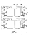
- image sensors 10 typically include pixels 20 having a photosensitive area or photodiode 30 for capturing incident light and associated circuitry 40 adjacent the photosensitive area for processing and the like.
- pixels 20 of an image sensor 10 are arranged asymmetrically to maximize the performance of the pixel while accommodating the associated circuitry 40.
- four of the pixels 20 typically form a regular grid pattern forming a supercell 50.
- a microlens 60 is positioned spanning and spatially centered over the "photosensitive portion" of the pixels 20.
- microlenses 65 may be positioned spanning and centered over the entire "pixel" creating a regular array of microlenses.
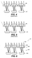
- microlens 60 Although the prior art arrangement of microlens 60 as in Fig. 2 is satisfactory, it includes drawbacks in that the microlens 60 is a small fraction of the area of the pixel, and therefore the photodiode 30 captures a small fraction of the incident light.
- microlenses 65 (as in Fig. 3 ) over asymmetrically positioned pixels is satisfactory, they also include drawbacks.
- Fig. 4 as long as photodiodes 30 are symmetric with respect to the microlens 60 such as being centered in the pixel, then the performance of all pixels degrade in the same manner as the angle of the incident light is increased.
- Fig. 5 light passing (indicated by the dashed lines) through the microlenses 65 at certain angles is not directed onto the photodiode 30 causing undesirable degradation of the captured image when the photodiodes 30 are not arranged symmetrically with the microlens.
- the present invention is directed to overcoming one or more of the problems set forth above.
- the invention provides in an image sensor as defined by Claim 1. Possible specific embodiments are indicated in dependent claims.
- the present invention has the advantage of increasing the light gathering capacity of a pixel array and eliminating artifacts that occur when the incident angle of illumination is varied or varies. It is also includes the advantage of permitting more design freedom for efficient use of the pixel space.
- FIGs. 6 and 7 there are shown a side view and a top view of an image sensor 70 having a plurality or array of microlenses 80 of the present invention positioned respectively spanning a plurality of pixels 90 each having a photosensitive area or photodiode 100.
- the pixels 90 are arranged asymmetrically.
- pixels are grouped together so as to form an array of supercells 110.
- only two supercells 110a and 110b each comprising two pixels is shown for clarity in Figs. 6 and 7 .
- the photosensitive areas 100 are disposed along a top portion of a silicon substrate, as is well known in the art.
- the pixels 90 are arranged so that by design they include an asymmetrical arrangement of the photosensitive areas 100.
- An optical surface 120 of the microlens 130 is asymmetrically shaped.
- Prior art microlens (60 and 65) are substantially hemispherically shaped.
- the microlens 130 of the present invention is substantially a truncated hemisphere that allows an asymmetrical arrangement.
- the each microlens 130 includes a substantially arcuate-shaped portion along a peripheral edge and includes two substantially straight portions positioned substantially perpendicular to each other along a remaining edge.
- microlens 130 has been trimmed along one or more edges as compared to the prior art microlens (60 and 65). This aligns the optical axis of the microlens 130 with the photodiode 100.
- Fig. 7 it is noted that, within the two pixels comprising the supercell 110, the microlenses 130 abut each other so that each individual microlens (130a, 130b, 130c and 130d) is symmetry with respect to an imaginary y-axis of the supercell 110, but still not symmetrical within any individual pixel 90 as stated hereinabove.
- each two-pixel supercell 110 includes two asymmetrical-shaped microlenses 130 grouped spanning a supercell 110 and a pair of straight portions, one from each microlens, are positioned so that a peripheral portion formed by the two microlenses is two arcuate-shaped edges and two straight edges
- the above-described pixel array functions so that incoming light that passes through a microlens 130 is directed substantially uniformly, that is consistently from pixel to pixel, onto the photodiode 100, as illustrated by the solid and dashed lines, even though the spacing (i.e., distance) from photodiode to photodiode is not constant or is varying.
- the light is distributed substantially consistently across the photodiode 100 independent of which pixel within the supercell it is, with light passing from substantially directly overhead being directed substantially consistently onto a portion of the photodiode 100 and light that passes at angles through the microlens 130 is directed substantially consistently onto portions of the photodiode 100.
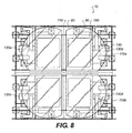
- FIG. 8 an alternative embodiment of the supercell 110 arrangement is shown.
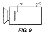
- FIG. 9 there is shown a side view of a digital camera 140 containing the image sensor 70 of the present invention for illustrating a typical commercial embodiment.
Landscapes
- Physics & Mathematics (AREA)
- General Physics & Mathematics (AREA)
- Optics & Photonics (AREA)
- Transforming Light Signals Into Electric Signals (AREA)
- Solid State Image Pick-Up Elements (AREA)
Applications Claiming Priority (3)
| Application Number | Priority Date | Filing Date | Title |
|---|---|---|---|
| US68610605P | 2005-06-01 | 2005-06-01 | |
| US11/253,915 US7456380B2 (en) | 2005-06-01 | 2005-10-18 | Asymmetrical microlenses on pixel arrays |
| PCT/US2006/020585 WO2006130517A1 (en) | 2005-06-01 | 2006-05-26 | Asymmetrical microlenses on pixel arrays |
Publications (2)
| Publication Number | Publication Date |
|---|---|
| EP1894253A1 EP1894253A1 (en) | 2008-03-05 |
| EP1894253B1 true EP1894253B1 (en) | 2011-07-13 |
Family
ID=36809127
Family Applications (1)
| Application Number | Title | Priority Date | Filing Date |
|---|---|---|---|
| EP06771388A Active EP1894253B1 (en) | 2005-06-01 | 2006-05-26 | Asymmetrical microlenses on pixel arrays |
Country Status (7)
Families Citing this family (14)
| Publication number | Priority date | Publication date | Assignee | Title |
|---|---|---|---|---|
| US7456380B2 (en) * | 2005-06-01 | 2008-11-25 | Eastman Kodak Company | Asymmetrical microlenses on pixel arrays |
| JP2007208817A (ja) * | 2006-02-03 | 2007-08-16 | Toshiba Corp | 固体撮像装置 |
| JP5277565B2 (ja) * | 2007-05-31 | 2013-08-28 | 富士通セミコンダクター株式会社 | 固体撮像素子 |
| US9153614B2 (en) * | 2007-08-15 | 2015-10-06 | Micron Technology, Inc. | Method and apparatus for lens alignment for optically sensitive devices and systems implementing same |
| JP2009289927A (ja) * | 2008-05-28 | 2009-12-10 | Panasonic Corp | 固体撮像装置及びその製造方法 |
| JP2009302483A (ja) * | 2008-06-17 | 2009-12-24 | Panasonic Corp | 固体撮像装置及びその製造方法 |
| US9444985B2 (en) | 2012-05-03 | 2016-09-13 | Semiconductor Components Industries, Llc | Reduced height camera modules |
| KR101944757B1 (ko) | 2014-10-31 | 2019-02-01 | 후아웨이 테크놀러지 컴퍼니 리미티드 | 파일 액세스 방법, 시스템, 및 호스트 |
| US9911774B2 (en) * | 2015-04-14 | 2018-03-06 | Massachusetts Institute Of Technology | Photodiode placement for cross talk suppression |
| US9936129B2 (en) | 2016-06-15 | 2018-04-03 | Obsidian Sensors, Inc. | Generating high resolution images |
| US10015389B2 (en) * | 2016-09-22 | 2018-07-03 | Omnivision Technologies, Inc. | Image sensor with asymmetric-microlens phase-detection auto-focus (PDAF) detectors, associated PDAF imaging system, and associated method |
| EP4139641A1 (en) | 2020-04-24 | 2023-03-01 | Meta Platforms Technologies, Llc | Polarimetric imaging camera |
| US20220139990A1 (en) * | 2020-11-04 | 2022-05-05 | Facebook Technologies, Llc | Polarimetric imaging camera |
| KR102629588B1 (ko) * | 2021-11-02 | 2024-01-25 | 삼성전자주식회사 | 나노 광학 마이크로렌즈 어레이를 구비하는 광학 센서 및 이를 포함하는 전자 장치 |
Family Cites Families (8)
| Publication number | Priority date | Publication date | Assignee | Title |
|---|---|---|---|---|
| US5536455A (en) * | 1994-01-03 | 1996-07-16 | Omron Corporation | Method of manufacturing lens array |
| DE19545484C2 (de) | 1995-12-06 | 2002-06-20 | Deutsche Telekom Ag | Bildaufnahmeeinrichtung |
| US6829087B2 (en) * | 1998-04-15 | 2004-12-07 | Bright View Technologies, Inc. | Micro-lens array based light transmitting screen with tunable gain |
| AU2001218821A1 (en) | 2000-12-14 | 2002-06-24 | 3Dv Systems Ltd. | 3d camera |
| US6709796B2 (en) * | 2002-06-12 | 2004-03-23 | Eastman Kodak Company | Camera speed color film with base side micro-lenses |
| US7227692B2 (en) * | 2003-10-09 | 2007-06-05 | Micron Technology, Inc | Method and apparatus for balancing color response of imagers |
| US7456380B2 (en) * | 2005-06-01 | 2008-11-25 | Eastman Kodak Company | Asymmetrical microlenses on pixel arrays |
| TWM289853U (en) * | 2005-11-02 | 2006-04-21 | Pixart Imaging Inc | Socket for testing image sensor |
-
2005
- 2005-10-18 US US11/253,915 patent/US7456380B2/en active Active
-
2006
- 2006-05-23 TW TW095118203A patent/TWI406425B/zh active
- 2006-05-26 CN CN2006800194208A patent/CN101189731B/zh active Active
- 2006-05-26 EP EP06771388A patent/EP1894253B1/en active Active
- 2006-05-26 KR KR1020077027729A patent/KR101274305B1/ko active Active
- 2006-05-26 WO PCT/US2006/020585 patent/WO2006130517A1/en active Application Filing
- 2006-05-26 JP JP2008514727A patent/JP4884465B2/ja active Active
Also Published As
| Publication number | Publication date |
|---|---|
| US7456380B2 (en) | 2008-11-25 |
| US20060273239A1 (en) | 2006-12-07 |
| KR101274305B1 (ko) | 2013-06-13 |
| EP1894253A1 (en) | 2008-03-05 |
| TWI406425B (zh) | 2013-08-21 |
| TW200711156A (en) | 2007-03-16 |
| JP2008546200A (ja) | 2008-12-18 |
| KR20080019598A (ko) | 2008-03-04 |
| WO2006130517A1 (en) | 2006-12-07 |
| CN101189731B (zh) | 2012-10-10 |
| JP4884465B2 (ja) | 2012-02-29 |
| CN101189731A (zh) | 2008-05-28 |
Similar Documents
| Publication | Publication Date | Title |
|---|---|---|
| EP1894253B1 (en) | Asymmetrical microlenses on pixel arrays | |
| US9070799B2 (en) | Solid state imaging device with microlens shifted from the center of the photo diode | |
| EP2083447B1 (en) | Image pickup apparatus | |
| CN101490845B (zh) | 固态图像捕获设备及其制造方法以及电子信息设备 | |
| EP2083446B1 (en) | Image pickup apparatus | |
| CN103081457B (zh) | 固态成像装置 | |
| EP1712087B1 (en) | Thin camera having sub-pixel resolution | |
| US7865076B2 (en) | Compound eye-camera module | |
| CN104425635A (zh) | 使用显微透镜的相位差检测像素 | |
| JPH08107194A (ja) | 固体撮像装置 | |
| EP2388987A1 (en) | Camera with volumetric sensor chip | |
| JP2016219469A (ja) | 固体撮像装置およびカメラ | |
| CN104183612B (zh) | 一种光路倾斜的cmos图像传感器的像素阵列 | |
| US20080191299A1 (en) | Microlenses for irregular pixels | |
| KR20040041066A (ko) | 고체촬상소자 | |
| US7227193B2 (en) | Solid-state image sensor with micro-lenses for preventing shading | |
| KR20060043228A (ko) | 촬상 장치 및 그 배열 방법 | |
| EP4390340B1 (en) | An imaging device, an imaging system and a method for wavelength dependent imaging | |
| US9257469B2 (en) | Color imaging device | |
| JP6990101B2 (ja) | 撮像素子 | |
| JP3604116B2 (ja) | 固体撮像装置 | |
| EP4280281A1 (en) | Image sensor | |
| JP6248417B2 (ja) | 撮像素子およびカメラ | |
| KR20070075567A (ko) | 프리즘을 이용하는 고감도 이미지 센서 | |
| WO2005053036A1 (en) | Large pixel micro-lens |
Legal Events
| Date | Code | Title | Description |
|---|---|---|---|
| PUAI | Public reference made under article 153(3) epc to a published international application that has entered the european phase |
Free format text: ORIGINAL CODE: 0009012 |
|
| 17P | Request for examination filed |
Effective date: 20071208 |
|
| AK | Designated contracting states |
Kind code of ref document: A1 Designated state(s): DE FR GB NL |
|
| 17Q | First examination report despatched |
Effective date: 20040317 |
|
| R17C | First examination report despatched (corrected) |
Effective date: 20080317 |
|
| RBV | Designated contracting states (corrected) |
Designated state(s): DE FR GB NL |
|
| DAX | Request for extension of the european patent (deleted) | ||
| GRAP | Despatch of communication of intention to grant a patent |
Free format text: ORIGINAL CODE: EPIDOSNIGR1 |
|
| RIC1 | Information provided on ipc code assigned before grant |
Ipc: H01L 27/146 20060101AFI20110110BHEP |
|
| GRAS | Grant fee paid |
Free format text: ORIGINAL CODE: EPIDOSNIGR3 |
|
| GRAA | (expected) grant |
Free format text: ORIGINAL CODE: 0009210 |
|
| AK | Designated contracting states |
Kind code of ref document: B1 Designated state(s): DE FR GB NL |
|
| REG | Reference to a national code |
Ref country code: GB Ref legal event code: FG4D |
|
| REG | Reference to a national code |
Ref country code: DE Ref legal event code: R096 Ref document number: 602006023085 Country of ref document: DE Effective date: 20110908 |
|
| REG | Reference to a national code |
Ref country code: NL Ref legal event code: T3 |
|
| REG | Reference to a national code |
Ref country code: DE Ref legal event code: R082 Ref document number: 602006023085 Country of ref document: DE Representative=s name: LEINWEBER & ZIMMERMANN, DE |
|
| REG | Reference to a national code |
Ref country code: DE Ref legal event code: R082 Ref document number: 602006023085 Country of ref document: DE Representative=s name: LEINWEBER & ZIMMERMANN, DE Effective date: 20111219 Ref country code: DE Ref legal event code: R081 Ref document number: 602006023085 Country of ref document: DE Owner name: OMNIVISION TECHNOLOGIES, INC., SANTA CLARA, US Free format text: FORMER OWNER: EASTMAN KODAK COMPANY, ROCHESTER, N.Y., US Effective date: 20111219 |
|
| PLBE | No opposition filed within time limit |
Free format text: ORIGINAL CODE: 0009261 |
|
| STAA | Information on the status of an ep patent application or granted ep patent |
Free format text: STATUS: NO OPPOSITION FILED WITHIN TIME LIMIT |
|
| 26N | No opposition filed |
Effective date: 20120416 |
|
| REG | Reference to a national code |
Ref country code: DE Ref legal event code: R097 Ref document number: 602006023085 Country of ref document: DE Effective date: 20120416 |
|
| REG | Reference to a national code |
Ref country code: FR Ref legal event code: PLFP Year of fee payment: 11 |
|
| REG | Reference to a national code |
Ref country code: FR Ref legal event code: PLFP Year of fee payment: 12 |
|
| REG | Reference to a national code |
Ref country code: FR Ref legal event code: PLFP Year of fee payment: 13 |
|
| REG | Reference to a national code |
Ref country code: FR Ref legal event code: PLFP Year of fee payment: 18 |
|
| REG | Reference to a national code |
Ref country code: DE Ref legal event code: R079 Ref document number: 602006023085 Country of ref document: DE Free format text: PREVIOUS MAIN CLASS: H01L0027146000 Ipc: H10F0039180000 |
|
| PGFP | Annual fee paid to national office [announced via postgrant information from national office to epo] |
Ref country code: NL Payment date: 20250421 Year of fee payment: 20 |
|
| PGFP | Annual fee paid to national office [announced via postgrant information from national office to epo] |
Ref country code: DE Payment date: 20250409 Year of fee payment: 20 |
|
| PGFP | Annual fee paid to national office [announced via postgrant information from national office to epo] |
Ref country code: GB Payment date: 20250410 Year of fee payment: 20 |
|
| PGFP | Annual fee paid to national office [announced via postgrant information from national office to epo] |
Ref country code: FR Payment date: 20250409 Year of fee payment: 20 |