US9257469B2 - Color imaging device - Google Patents
Color imaging device Download PDFInfo
- Publication number
- US9257469B2 US9257469B2 US14/353,113 US201214353113A US9257469B2 US 9257469 B2 US9257469 B2 US 9257469B2 US 201214353113 A US201214353113 A US 201214353113A US 9257469 B2 US9257469 B2 US 9257469B2
- Authority
- US
- United States
- Prior art keywords
- light
- refractive index
- high refractive
- portions
- imaging apparatus
- Prior art date
- Legal status (The legal status is an assumption and is not a legal conclusion. Google has not performed a legal analysis and makes no representation as to the accuracy of the status listed.)
- Expired - Fee Related, expires
Links
- 238000003384 imaging method Methods 0.000 title claims abstract description 69
- 230000003287 optical effect Effects 0.000 description 29
- 238000010586 diagram Methods 0.000 description 19
- 238000002834 transmittance Methods 0.000 description 16
- 230000000694 effects Effects 0.000 description 10
- 238000009826 distribution Methods 0.000 description 8
- 238000000034 method Methods 0.000 description 8
- 239000000463 material Substances 0.000 description 4
- 238000010276 construction Methods 0.000 description 3
- 230000007423 decrease Effects 0.000 description 3
- 230000010287 polarization Effects 0.000 description 3
- 229910052581 Si3N4 Inorganic materials 0.000 description 2
- 230000005684 electric field Effects 0.000 description 2
- 230000002708 enhancing effect Effects 0.000 description 2
- 230000004907 flux Effects 0.000 description 2
- 229920002120 photoresistant polymer Polymers 0.000 description 2
- HQVNEWCFYHHQES-UHFFFAOYSA-N silicon nitride Chemical compound N12[Si]34N5[Si]62N3[Si]51N64 HQVNEWCFYHHQES-UHFFFAOYSA-N 0.000 description 2
- 238000003892 spreading Methods 0.000 description 2
- GWEVSGVZZGPLCZ-UHFFFAOYSA-N Titan oxide Chemical compound O=[Ti]=O GWEVSGVZZGPLCZ-UHFFFAOYSA-N 0.000 description 1
- 230000004075 alteration Effects 0.000 description 1
- 238000004380 ashing Methods 0.000 description 1
- 230000015572 biosynthetic process Effects 0.000 description 1
- 238000006243 chemical reaction Methods 0.000 description 1
- 239000012141 concentrate Substances 0.000 description 1
- 239000000470 constituent Substances 0.000 description 1
- 239000010408 film Substances 0.000 description 1
- 230000001939 inductive effect Effects 0.000 description 1
- 238000004519 manufacturing process Methods 0.000 description 1
- BPUBBGLMJRNUCC-UHFFFAOYSA-N oxygen(2-);tantalum(5+) Chemical compound [O-2].[O-2].[O-2].[O-2].[O-2].[Ta+5].[Ta+5] BPUBBGLMJRNUCC-UHFFFAOYSA-N 0.000 description 1
- 238000000206 photolithography Methods 0.000 description 1
- 239000004065 semiconductor Substances 0.000 description 1
- 230000035945 sensitivity Effects 0.000 description 1
- 238000001228 spectrum Methods 0.000 description 1
- 239000000126 substance Substances 0.000 description 1
- 229910001936 tantalum oxide Inorganic materials 0.000 description 1
- 239000010409 thin film Substances 0.000 description 1
- OGIDPMRJRNCKJF-UHFFFAOYSA-N titanium oxide Inorganic materials [Ti]=O OGIDPMRJRNCKJF-UHFFFAOYSA-N 0.000 description 1
- 239000012780 transparent material Substances 0.000 description 1
Images


Classifications
-
- H—ELECTRICITY
- H01—ELECTRIC ELEMENTS
- H01L—SEMICONDUCTOR DEVICES NOT COVERED BY CLASS H10
- H01L27/00—Devices consisting of a plurality of semiconductor or other solid-state components formed in or on a common substrate
- H01L27/14—Devices consisting of a plurality of semiconductor or other solid-state components formed in or on a common substrate including semiconductor components sensitive to infrared radiation, light, electromagnetic radiation of shorter wavelength or corpuscular radiation and specially adapted either for the conversion of the energy of such radiation into electrical energy or for the control of electrical energy by such radiation
- H01L27/144—Devices controlled by radiation
- H01L27/146—Imager structures
- H01L27/14601—Structural or functional details thereof
- H01L27/14625—Optical elements or arrangements associated with the device
-
- H—ELECTRICITY
- H01—ELECTRIC ELEMENTS
- H01L—SEMICONDUCTOR DEVICES NOT COVERED BY CLASS H10
- H01L27/00—Devices consisting of a plurality of semiconductor or other solid-state components formed in or on a common substrate
- H01L27/14—Devices consisting of a plurality of semiconductor or other solid-state components formed in or on a common substrate including semiconductor components sensitive to infrared radiation, light, electromagnetic radiation of shorter wavelength or corpuscular radiation and specially adapted either for the conversion of the energy of such radiation into electrical energy or for the control of electrical energy by such radiation
- H01L27/144—Devices controlled by radiation
- H01L27/146—Imager structures
- H01L27/14601—Structural or functional details thereof
- H01L27/1462—Coatings
- H01L27/14623—Optical shielding
-
- H—ELECTRICITY
- H01—ELECTRIC ELEMENTS
- H01L—SEMICONDUCTOR DEVICES NOT COVERED BY CLASS H10
- H01L27/00—Devices consisting of a plurality of semiconductor or other solid-state components formed in or on a common substrate
- H01L27/14—Devices consisting of a plurality of semiconductor or other solid-state components formed in or on a common substrate including semiconductor components sensitive to infrared radiation, light, electromagnetic radiation of shorter wavelength or corpuscular radiation and specially adapted either for the conversion of the energy of such radiation into electrical energy or for the control of electrical energy by such radiation
- H01L27/144—Devices controlled by radiation
- H01L27/146—Imager structures
- H01L27/14643—Photodiode arrays; MOS imagers
- H01L27/14645—Colour imagers
-
- H—ELECTRICITY
- H04—ELECTRIC COMMUNICATION TECHNIQUE
- H04N—PICTORIAL COMMUNICATION, e.g. TELEVISION
- H04N23/00—Cameras or camera modules comprising electronic image sensors; Control thereof
- H04N23/10—Cameras or camera modules comprising electronic image sensors; Control thereof for generating image signals from different wavelengths
- H04N23/13—Cameras or camera modules comprising electronic image sensors; Control thereof for generating image signals from different wavelengths with multiple sensors
- H04N23/16—Optical arrangements associated therewith, e.g. for beam-splitting or for colour correction
-
- H04N9/045—
-
- H04N9/097—
Definitions
- the present application relates to a technique of enhancing the sensitivity of an imaging apparatus.
- miniaturized cell sizes introduce a physical decrease in the geometric area in which light is received, thus lowering the amount of received light. Therefore, what is needed in the future is imaging structures for introducing an increase, even if only a little, in the efficiency of light utilization.
- Patent Document 1 proposes an imaging apparatus without color filters which is meant to provide an improved efficiency of light utilization.
- Light entering the imaging apparatus passes through a plate-like transparent spectroscopic portion which has a higher refractive index than do the surroundings, whereby 0 th order light and ⁇ 1 st order light of respectively different wavelengths occur. It is designed so that the resultant 0 th order light and ⁇ 1 st order light enter respectively different photodetectors.
- the proposal is to, by using such a transparent spectroscopic portion, enhance the efficiency of light utilization over that of conventional imaging apparatuses in which color filters are employed.
- Patent Document 2 discloses an inner-layer lens as a converging device in an imaging apparatus, where light convergence is enhanced through a lens effect.
- Patent Document 3 discloses an optical waveguide, as a converging device in an imaging apparatus.
- An imaging apparatus comprises a plurality of photodetecting portions; a transparent layer provided at the side of a light-receiving surface of the plurality of photodetecting portions; a plurality of spectroscopic portions provided between a light-entering surface of the transparent layer and the plurality of photodetecting portions; and a plurality of high refractive index transparent members disposed closer to the plurality of photodetecting portions than are the plurality of spectroscopic portions, wherein the plurality of high refractive index transparent members have a higher refractive index than does the transparent layer.
- high refractive index transparent members are disposed closer to photodetecting portions than are spectroscopic portions. As a result, light from around the high refractive index transparent members is converged, thereby allowing light to efficiently enter an aperture region which is restricted by light shielding portions.
- FIG. 1 A diagram showing a construction in which spectroscopic portions are applied to an imaging apparatus.
- FIG. 2 A diagram showing the optical characteristics of light entering photodetectors in the case where light shielding portions exist in an imaging apparatus and in the case where they don't.
- FIG. 3 A diagram showing an imaging apparatus according to an exemplary embodiment.
- FIG. 4 A diagram showing the optical characteristics of light entering photodetectors in the case where high refractive index members according to an exemplary embodiment exist and in the case where they don't.
- FIG. 5 A diagram showing the three-dimensional shape of a high refractive index member according to an exemplary embodiment.
- FIG. 6 ( a ) to ( d ) are diagrams showing a method of producing a high refractive index member according to an exemplary embodiment.
- FIG. 7 A diagram showing an imaging apparatus according to an exemplary embodiment.
- FIG. 8 A diagram showing the optical characteristics of light entering photodetectors in the case where high refractive index members according to an exemplary embodiment exist and in the case where they don't.
- FIG. 9 A diagram showing the optical characteristics of light entering photodetectors in the case where light shielding portions exist and in the case where they don't, in an exemplary embodiment.
- FIG. 10 A diagram showing an imaging apparatus according to an exemplary embodiment.
- FIG. 11 A diagram showing relationships between the radius of curvature of an on-chip lens and the optical characteristics of light entering photodetectors in an exemplary embodiment.
- FIG. 12 A diagram showing the optical characteristics of light entering photodetectors in the case where high refractive index members according to an exemplary embodiment exist and in the case where they don't.
- FIG. 13 A diagram showing an imaging apparatus according to an exemplary embodiment.
- FIG. 14 A diagram showing an imaging apparatus according to an exemplary embodiment.
- FIG. 15 A diagram showing a cross-sectional intensity distribution of light when light enters a spectroscopic portion according to an exemplary embodiment.
- FIG. 16 A diagram showing a light intensity distribution at the light-receiving surface of photodetectors according to an exemplary embodiment.
- FIG. 17 A diagram showing an imaging apparatus according to an exemplary embodiment.
- FIG. 18 A diagram showing a cross-sectional intensity distribution of light when light enters a spectroscopic portion according to an exemplary embodiment.
- FIG. 19 A diagram showing a light intensity distribution at the light-receiving surface of photodetectors according to an exemplary embodiment.
- FIG. 1 is a cross-sectional view of a construction in which the spectroscopic portion described in Patent Document 1 is applied to a generic imaging apparatus.
- the imaging apparatus 1 shown in FIG. 1 includes: spectroscopic portions 3 being embedded in a transparent layer 2 and composed of a material which has a higher refractive index than that of the transparent layer 2 ; imaginary light shielding portions 4 , which are meant to be interconnects, electrodes, and the like; and photodetectors 5 a and 5 b .
- a phase difference occurs between the light passing through any spectroscopic portion 3 , which is of a high refractive index material, and the light passing through the surrounding transparent layer 2 .
- the length (i.e., length along the optical axis direction) of the spectroscopic portion 3 is adjusted so that red light is separated as ⁇ 1 st order light and that cyan light, which results by removing red from white, occurs as 0 th order light.
- the spectroscopic portions 3 are disposed so as to correspond to every other one of the plurality of photodetectors (i.e., one for every two pixels).
- FIG. 2 shows the incident optical characteristics on the photodetectors 5 a and 5 b in the case where the light shielding portions 4 exist in the imaging apparatus 1 and where they don't.
- transmittance is represented as a value obtained by normalizing the light amount incident to each photodetector by the light amount incident to one pixel, for each wavelength.
- the light transmittance on each photodetector is greatly reduced because of the aperture being restricted by the light shielding portions 4 .
- One non-limiting, and exemplary embodiment of the present application provides an imaging apparatus with an enhanced efficiency of light utilization.
- An imaging apparatus comprises: a plurality of photodetecting portions; a transparent layer provided at the side of a light-receiving surface of the plurality of photodetecting portions; a plurality of spectroscopic portions provided between a light-entering surface of the transparent layer and the plurality of photodetecting portions; and a plurality of high refractive index transparent members disposed closer to the plurality of photodetecting portions than are the plurality of spectroscopic portions, wherein the plurality of high refractive index transparent members have a higher refractive index than does the transparent layer.
- each spectroscopic portion is shaped so that a length thereof along a direction which is perpendicular to the light-receiving surface is longer than a length thereof along a direction which is parallel to the light-receiving surface; and each high refractive index transparent member is shaped so that a length thereof along a direction which is parallel to the light-receiving surface is longer than a length thereof along a direction which is perpendicular to the light-receiving surface.
- the spectroscopic portions are disposed so as to correspond to every other one of the plurality of photodetecting portions; and the high refractive index transparent members are disposed so as to correspond respectively to the plurality of photodetecting portions.
- the spectroscopic portions and the high refractive index transparent members are disposed so as to correspond respectively to the plurality of photodetecting portions.
- a light shielding portion is provided at a boundary portion between the photodetecting portions.
- the high refractive index transparent members are provided above those areas of the light-receiving surface of the plurality of photodetecting portions where the light shielding portion is not provided.
- an on-chip lens is provided at the side of the light-entering surface of the transparent layer.
- a face of each high refractive index transparent member along a direction which is parallel to the light-receiving surface is rectangular or circular.
- orthogonal projections of the plurality of spectroscopic portions onto the light-receiving surface do not overlap those of the plurality of high refractive index transparent members.
- +1 st order diffracted light and ⁇ 1 st order diffracted light into which light is separated as the light passes through the transparent layer and one of the spectroscopic portions, are incident on respectively different ones of the photodetecting portions; and the high refractive index transparent members are disposed so that diffraction angles of the +1 st order diffracted light and the ⁇ 1 st order diffracted light become more spread than without the high refractive index transparent members.
- the high refractive index transparent members are disposed at positions which are closer to the spectroscopic portions than to the light-receiving surface.
- FIG. 3 is a cross-sectional view showing an imaging apparatus 10 according to Embodiment 1 of the present invention.
- like constituent elements will be denoted by like reference numerals, and the same description will not be repeated.
- the pixel cell size is supposed to be 1.4 ⁇ m.
- the imaging apparatus 10 includes a plurality of photodetectors 5 a and 5 b , a transparent layer 2 provided at the side of the light-receiving surface 15 a , 15 b of the photodetectors 5 a and 5 b , a plurality of spectroscopic portions 3 provided between a light-entering surface 2 a of the transparent layer 2 and the photodetectors 5 a and 5 b , and a plurality of high refractive index transparent members 6 provided closer to the photodetectors 5 a and 5 b than are the spectroscopic portions 3 .
- Light shielding portions 4 are provided at boundary portions between photodetectors.
- the photodetectors 5 a and 5 b which are disposed in a one-dimensional or two-dimensional arrangement, function as photodetecting portions which receive light and output an electrical signal in accordance with the amount of light.
- the transparent layer 2 is a layer which is transparent in a visible light region of wavelengths from 400 nm to 700 nm.
- the spectroscopic portions 3 are covered by the transparent layer 2 .
- the light shielding portions 4 are arranged so that the photodetectors have an aperture ratio of 40%.
- the spectroscopic portions 3 are disposed so as to correspond to every other one of the plurality of photodetectors 5 a and 5 b . In other words, spectroscopic portions 3 are disposed on a one-for-every-two-pixels basis.
- the high refractive index transparent members 6 are disposed so as to correspond respectively to the plurality of photodetectors 5 a and 5 b.
- Each spectroscopic portion 3 is shaped so that its length along a direction (optical axis direction) which is perpendicular to the light-receiving surface 15 a , 15 b is longer than its length along a direction which is parallel to the light-receiving surface 15 a , 15 b .
- Each high refractive index transparent member 6 is shaped so that its length along a direction which is parallel to the light-receiving surface 15 a , 15 b is longer than its length along a direction (optical axis direction) which is perpendicular to the light-receiving surface 15 a , 15 b.
- the plate-like high refractive index transparent members (hereinafter referred to as high refractive index members) 6 are covered with the transparent layer 2 , and are transparent in the visible light region.
- the high refractive index members 6 have a higher refractive index than does the transparent layer 2 .
- the high refractive index members 6 are disposed above those areas of the light-receiving surface of the plurality of photodetectors 5 a and 5 b where the light shielding portions 4 are not provided.
- each high refractive index member 6 is disposed so that, when viewed from the optical axis direction, large part of it overlaps an area where no light shielding portions 4 are provided.
- the transparent layer 2 has a refractive index of 1.46, and that the thickness from the lower end of each spectroscopic portion 3 to a photodetector 5 a , 5 b is 3.0 ⁇ m. It is preferable that, when light entering the imaging apparatus 10 has an incident angle of 0 degrees (i.e., perpendicular to the light-entering surface 2 a ), the structural center of each high refractive index member 6 is located upon the center axis of the aperture.
- FIG. 4 shows the optical characteristics of light entering the surface of the photodetectors 5 a and 5 b , assuming that the high refractive index members 6 have a refractive index of 2.00, a height T ( FIG. 5 ) of 0.2 ⁇ m, and a width w ( FIG. 5 ) of 1.0 ⁇ m, and that the distance between the photodetector surface and the lower face of each high refractive index member 6 is 0.4 ⁇ m. It can be seen that deploying the high refractive index members 6 improves the light transmittance of the photodetectors 5 a and 5 b.
- ⁇ 0 represents the dielectric constant in a vacuum.
- ⁇ represents electric susceptibility.
- P ⁇ 0 ⁇ E.
- FIG. 5 shows a three-dimensional shape of a high refractive index member 6 in the present embodiment. It has a rectangular planar shape and a rectangular cross-sectional shape. Ensuring this makes it unnecessary to include complicated steps in the semiconductor process.
- FIG. 6 shows a method of producing the high refractive index members 6 .
- a high refractive index layer 6 a is deposited on a transparent layer 2 , upon which a photoresist 7 a is deposited.
- a resist pattern 7 b is formed through photolithography.
- the underlying high refractive index layer 6 a is etched concurrently with the resist pattern 7 b , and the remaining resist pattern 7 b is removed by ashing or the like, thus forming the high refractive index member 6 on the transparent layer 2 .
- the transparent layer 2 is deposited by a CVD technique or the like, whereby the high refractive index member 6 embedded in the transparent layer 2 is formed.
- An example of a converging device in a conventional imaging apparatus is an inner-layer lens as described in Patent Document 2.
- This has a spherical or aspherical cross-sectional shape, such that light convergence is enhanced through a lens effect. Therefore, in Patent Document 2, it is important to optimize the cross section of the inner-layer lens so as to be spherical or aspherical. From any such device utilizing a lens effect, the present embodiment differs in that convergence is effected based only on a refractive index difference with respect to the surroundings. Moreover, a lens-like cross-sectional shape is not needed in the present embodiment. This makes for a simplified process, e.g., by eliminating the photoresist reflow step that would be involved in the fabrication process of an inner-layer lens.
- optical waveguide Another converging device in a conventional imaging apparatus is the optical waveguide described in Patent Document 3.
- the interstices between interconnection layers within a pixel region are buried with a high, refractive index material to form an optical waveguide.
- the optical waveguide is composed of a core with a high refractive index and a clad having a lower refractive index than that of the core. Even if incident oblique light collides against a wall of the optical waveguide, it is allowed to efficiently enter the aperture region of a photodetector via total reflection. Therefore, the length of the optical waveguide along the optical axis direction should preferably be as long as possible.
- the present embodiment is distinct from an optical waveguide because of featuring a shorter length along the optical axis direction than the width. The reason is that, rather than utilizing total reflection, the present embodiment utilizes light convergence based on a refractive index difference from the surroundings. Therefore, elongation along the optical axis direction is not necessary; in fact, elongation along a parallel direction to the photodetector is preferable.
- the material of the high refractive index members 6 silicon nitride (SiN) or a transparent oxide such as tantalum oxide or titanium oxide may be used.
- SiN silicon nitride
- a transparent oxide such as tantalum oxide or titanium oxide
- the planar shape of the high refractive index members 6 may be circular or elliptical.
- each high refractive index member 6 As for the optical axis position of each high refractive index member 6 , it is preferably placed so as to allow light to be converged on the surface of the photodetector 5 a , 5 b.
- the imaging apparatus 10 of the present embodiment may be a CCD imaging apparatus or a CMOS imaging apparatus. In either case, an imaging apparatus having a large aperture is preferable, such that efficient incidence occurs of the light from the spectroscopic portions 3 and the light which is incident on the imaging apparatus 10 to directly enter the photodetectors.
- the high refractive index members 6 are provided for all pixels, they do not need to be provided for all pixels. They may be provided for any arbitrary pixel to increase the amount of light entering the photodetector for that pixel.
- the present embodiment deploys plate-like spectroscopic elements that generate diffracted light of the same color at the adjacent pixels, this being in order to demonstrate the effects of the high refractive index members 6 .
- a plate-like high refractive index transparent material having stepped portions as described in e.g. the pamphlet of International Publication No. 2010/016195, may also be combined.
- FIG. 7 is a cross-sectional view showing an imaging apparatus 11 according to Embodiment 2 of the present invention.
- the imaging apparatus 11 includes a spectroscopic portion 3 or 7 in every pixel.
- the spectroscopic portions 3 are disposed at pixels which include photodetectors 5 a , and are provided on a one-for-every-two-pixels basis along the x direction in the figure. Their spectroscopic characteristics are identical to those of the spectroscopic portions 3 in Embodiment 1.
- the other spectroscopic portions 7 are disposed at pixels which include photodetectors 5 b , and are provided on a one-for-every-two-pixels basis along the x direction in the figure. In other words, the spectroscopic portions 3 and the spectroscopic portions 7 alternate so that either a spectroscopic portion 3 or 7 is included in every pixel.
- the spectroscopic portions 7 separate blue light B as ⁇ 1 st order light from the incident white light, so that yellow light Y, which results from removing blue from white, occurs as the 0 th order light.
- FIG. 9 shows, under a scenario where no high refractive index members are employed, incident optical characteristics on the photodetectors 5 a and 5 b in the case where light shielding portions 4 exist in the imaging apparatus 11 and in the case where they don't.
- the light shielding portions do not exist, cyan light and blue light are incident on the photodetectors 5 a , so that the transmittance at 400 nm to 500 nm is significantly greater than the transmittance at 600 nm to 700 nm.
- the transmittance at 600 nm to 700 nm is significantly greater than the transmittance at 400 nm to 500 nm.
- FIG. 8 shows, in this Embodiment 2, the optical characteristics of light entering the photodetectors 5 a and 5 b in the case where the high refractive index members 6 are provided and in the case where they aren't.
- Embodiment 2 illustrates that the high refractive index members 6 have the same three-dimensional shape as that in FIG. 5 , they may have a circular or elliptical planar shape.
- FIG. 10 is a cross-sectional view showing an imaging apparatus 12 according to Embodiment 3 of the present invention.
- the pixel cell size is 1.4 ⁇ m.
- the imaging apparatus 12 differs from the imaging apparatus 10 of Embodiment 1 in that on-chip lenses 8 are provided at the side of the light-entering surface 2 a.
- FIG. 11 shows the optical characteristics of light entering the photodetectors 5 b , where the radius of curvature of the on-chip lenses is varied.
- the transmittance especially at wavelengths from 400 nm to 550 nm is increased.
- the radius of curvature is smaller than 1.30 ⁇ m, the transmittance at wavelengths from 400 nm to 550 nm increases to become about equal to or greater than the transmittance at wavelengths from 600 nm to 700 nm, whereby the color of the light entering the photodetectors 5 b is affected.
- the transmittance under a radius of curvature of 0.80 ⁇ m is smaller than the transmittance under a radius of curvature of 0.95 ⁇ m, thus indicating that light will not efficiently enter the photodetectors 5 b even if the radius of curvature of the on-chip lenses is made any smaller.
- 2.46 ⁇ m is selected as a radius of curvature under which the light entering the photodetectors 5 b takes on a red color even when on-chip lenses are employed.
- FIG. 12 shows a spectrum of light entering the photodetectors 5 a and 5 b when high refractive index members 6 of the same shape as that of Embodiment 1 are provided. It can be seen that the transmittance of light which is detected at each photodetector 5 b is increased at each wavelength. This is presumably because the high refractive index members 6 allow light from around the high refractive index members 6 to be converged on the central portions of the pixels, so that light is entering the photodetectors 5 b more efficiently.
- reflow lenses are employed as the on-chip lenses in the present embodiment, digital microlens which provide a similar convergence effect may also be employed.
- FIG. 13 is a cross-sectional view showing an imaging apparatus 13 according to Embodiment 4 of the present invention.
- orthogonal projections of the spectroscopic portions 3 onto the light-receiving surface do not overlap orthogonal projections of the high refractive index members 6 onto the light-receiving surface.
- the high refractive index members 6 are disposed at positions which are closer to the spectroscopic portions 3 than to the light-receiving surface.
- the high refractive index member 6 is disposed near the lower end of the spectroscopic portion 3 .
- the diffraction angles of ⁇ 1 st order diffracted light occurring from the spectroscopic portion 3 are increased over the case where no high refractive index member 6 is provided, and over the case where the high refractive index member 6 is disposed at a position which is close to the light-receiving surface.
- a spectroscopic portion 3 for separating incident red light R into ⁇ 1 st order light, a high refractive index member 6 , and photodetectors 5 a , 5 b , and 5 c are disposed as shown in FIG. 14 .
- the high refractive index member 6 is disposed only above the photodetector 5 c , and not above the photodetector 5 a . Note that the high refractive index member 6 has the same shape as in Embodiment 1.
- FIG. 15 shows a cross-sectional intensity distribution of light when, in the structure shown in FIG. 14 , red light with an Airy disk diameter of 2.2 ⁇ m is incident on the spectroscopic portion 3 .
- red light with an Airy disk diameter of 2.2 ⁇ m is incident on the spectroscopic portion 3 .
- red light passes through the spectroscopic portion 3 , it separates into diffracted light R 1 and R 2 . It can be seen that the diffraction angle of the diffracted light R 2 , which becomes separated toward the side where the high refractive index member 6 is provided, is greater than the diffraction angle of the diffracted light R 1 , which becomes separated toward the side where the high refractive index member 6 is not provided.
- FIG. 16 shows a light intensity distribution at the light-receiving surface 15 a , 15 b , 15 c of the photodetectors in FIG. 14 . Boundaries between the photodetectors are indicated by solid lines.
- the diffracted light R 1 and the diffracted light R 2 enter respectively different photodetectors. It can be seen that the diffracted light R 1 is incident astride the photodetectors 15 a and 15 b but that the diffracted light R 2 is incident concentratedly on the photodetector 15 c .
- Providing the high refractive index member 6 allows to increase the diffraction angle of the diffracted light R 2 so that it is incident on the desired photodetector.
- FIG. 17 is a cross-sectional view where the high refractive index member 6 of FIG. 14 is positioned 0.4 ⁇ m above the photodetector surface, in a manner similar to FIG. 3 illustrating the first embodiment.
- the high refractive index member 6 is placed at a position which is close to the light-receiving surface along the optical axis direction.
- the shapes of the spectroscopic portion 3 and the high refractive index member 6 are the same as those in FIG. 14 .
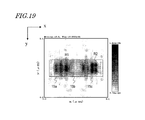
- FIG. 18 shows a cross-sectional intensity distribution of light when, in the structure of FIG. 17 , red light with an Airy disk diameter of 2.2 ⁇ m is incident on the spectroscopic portion 3 .
- FIG. 19 shows a light intensity distribution at the light-receiving surface 15 a , 15 b , 15 c of the photodetectors in FIG. 17 . It can be seen that the diffracted light R 2 is incident astride the photodetectors 15 b and 15 c .
- the high refractive index member 6 by disposing the high refractive index member 6 at a position which is closer to the spectroscopic portion 3 than to the light-receiving surface along the optical axis direction (e.g., near the lower end of the spectroscopic portion 3 ), there is provided an effect of widening the diffraction angles of the ⁇ 1 st order diffracted light. This makes it possible to narrow the interspace between the spectroscopic portion and the photodetectors that are disposed at predetermined interspaces, thereby reducing the thickness of the imaging device.
- Embodiments 1 to 4 above illustrate that the high refractive index members 6 have rectangular cross-sectional shapes, the effects of the present invention will be attained so long as a higher refractive index than that of the surroundings is available, even if shape alterations may occur due to the formation process of the high refractive index members 6 (e.g., the cross-sectional shape becoming trapezoidal, or having rounded corners).
- the imaging apparatus according to the present invention may be applied to both CMOS-type imaging devices and CCD-type imaging devices. Moreover, the imaging apparatus according to the present invention may be applied to imaging devices of a rear-irradiation type having interconnects embedded within Si, and to imaging devices in which an organic photoelectric conversion film is used.
- An imaging apparatus is especially useful in technological fields where imaging devices are employed, e.g., digital cameras, digital movie cameras, and imaging sensors.
Abstract
Description
- [Patent Document 1] the pamphlet of International Publication No. 2009/019818
- [Patent Document 2] Japanese Laid-Open Patent Publication No. 2011-103349
- [Patent Document 3] Japanese Laid-Open Patent Publication No. 2006-222270
D=∈0×E+P.
Herein, ∈0 represents the dielectric constant in a vacuum. Moreover, when a polarization P and an electric field E is expressible by a linear relationship, the electric flux density D can be expressed as, by using a relative dielectric constant and the vacuum dielectric constant ∈0:
D=∈×∈0×E
∈≡1+χ
Herein, χ represents electric susceptibility.
This permits the following expression:
P=∈0×χ×E.
On the other hand, the relative dielectric constant and the refractive index n are of the relationship:
∈=n2.
Therefore, the refractive index being large means the polarization P being large. Since polarization has a physical meaning of inducing light, light will concentrate in a region of a large refractive index n.
-
- 1, 10, 11, 12 imaging apparatus
- 2 transparent layer
- 2 a light-entering surface
- 3 spectroscopic portion
- 4 light shielding portion
- 5 a, 5 b photodetector
- 6 high refractive index transparent member
- 6 a high refractive index layer
- 8 on-chip lens
- 15 a, 15 b light-receiving surface
Claims (8)
Applications Claiming Priority (3)
| Application Number | Priority Date | Filing Date | Title |
|---|---|---|---|
| JP2011-233303 | 2011-10-24 | ||
| JP2011233303 | 2011-10-24 | ||
| PCT/JP2012/003647 WO2013061489A1 (en) | 2011-10-24 | 2012-06-04 | Color imaging device |
Publications (2)
| Publication Number | Publication Date |
|---|---|
| US20140263968A1 US20140263968A1 (en) | 2014-09-18 |
| US9257469B2 true US9257469B2 (en) | 2016-02-09 |
Family
ID=48167347
Family Applications (1)
| Application Number | Title | Priority Date | Filing Date |
|---|---|---|---|
| US14/353,113 Expired - Fee Related US9257469B2 (en) | 2011-10-24 | 2012-06-04 | Color imaging device |
Country Status (3)
| Country | Link |
|---|---|
| US (1) | US9257469B2 (en) |
| JP (1) | JP5975229B2 (en) |
| WO (1) | WO2013061489A1 (en) |
Families Citing this family (3)
| Publication number | Priority date | Publication date | Assignee | Title |
|---|---|---|---|---|
| KR102159166B1 (en) | 2014-05-09 | 2020-09-23 | 삼성전자주식회사 | Color separation device and image sensor including the color separation device |
| JP6602763B2 (en) * | 2014-07-25 | 2019-11-06 | 株式会社半導体エネルギー研究所 | Imaging device |
| CN117546293A (en) * | 2021-08-06 | 2024-02-09 | 索尼半导体解决方案公司 | Imaging element |
Citations (10)
| Publication number | Priority date | Publication date | Assignee | Title |
|---|---|---|---|---|
| JP2006222270A (en) | 2005-02-10 | 2006-08-24 | Sony Corp | Solid-state image sensor and its manufacturing method |
| US20080315074A1 (en) | 2007-06-21 | 2008-12-25 | Kabushiki Kaisha Toshiba | Array-type light receiving device and light collection method |
| WO2009019818A1 (en) | 2007-08-06 | 2009-02-12 | Panasonic Corporation | Light detecting device for imaging |
| US20090303371A1 (en) | 2008-06-09 | 2009-12-10 | Sony Corporation | Solid-state imaging device, drive method thereof and electronic apparatus |
| WO2009153937A1 (en) | 2008-06-18 | 2009-12-23 | パナソニック株式会社 | Solid-state imaging device |
| WO2010016195A1 (en) | 2008-08-05 | 2010-02-11 | パナソニック株式会社 | Photo-detection device used for image pickup |
| US20100289100A1 (en) | 2009-05-15 | 2010-11-18 | Sony Corporation | Solid-state image pickup device, method of manufacturing solid-state image pickup device, and electronic apparatus |
| JP2010287627A (en) | 2009-06-09 | 2010-12-24 | Canon Inc | Solid-state imaging apparatus |
| US20110096210A1 (en) | 2009-10-27 | 2011-04-28 | Sony Corporation | Solid-state imaging device, method of manufacturing solid-state imaging device, and electronic equipment |
| JP2011103349A (en) | 2009-11-10 | 2011-05-26 | Panasonic Corp | Solid-state imaging device and method of manufacturing the same |
Family Cites Families (3)
| Publication number | Priority date | Publication date | Assignee | Title |
|---|---|---|---|---|
| JP5013660B2 (en) * | 2004-03-29 | 2012-08-29 | キヤノン株式会社 | Image sensor |
| JP5055643B2 (en) * | 2008-07-28 | 2012-10-24 | 株式会社リコー | Image pickup device and image pickup apparatus |
| JPWO2011010455A1 (en) * | 2009-07-24 | 2012-12-27 | パナソニック株式会社 | Imaging apparatus and solid-state imaging device |
-
2012
- 2012-06-04 WO PCT/JP2012/003647 patent/WO2013061489A1/en active Application Filing
- 2012-06-04 JP JP2013540615A patent/JP5975229B2/en not_active Expired - Fee Related
- 2012-06-04 US US14/353,113 patent/US9257469B2/en not_active Expired - Fee Related
Patent Citations (15)
| Publication number | Priority date | Publication date | Assignee | Title |
|---|---|---|---|---|
| JP2006222270A (en) | 2005-02-10 | 2006-08-24 | Sony Corp | Solid-state image sensor and its manufacturing method |
| US20080315074A1 (en) | 2007-06-21 | 2008-12-25 | Kabushiki Kaisha Toshiba | Array-type light receiving device and light collection method |
| JP2009004533A (en) | 2007-06-21 | 2009-01-08 | Toshiba Corp | Array photodetector and light converging method |
| WO2009019818A1 (en) | 2007-08-06 | 2009-02-12 | Panasonic Corporation | Light detecting device for imaging |
| US20100176473A1 (en) | 2007-08-06 | 2010-07-15 | Panasonic Corporation | Imaging photodetection device |
| US20090303371A1 (en) | 2008-06-09 | 2009-12-10 | Sony Corporation | Solid-state imaging device, drive method thereof and electronic apparatus |
| US20100188537A1 (en) | 2008-06-18 | 2010-07-29 | Panasonic Corporation | Solid-state imaging device |
| WO2009153937A1 (en) | 2008-06-18 | 2009-12-23 | パナソニック株式会社 | Solid-state imaging device |
| WO2010016195A1 (en) | 2008-08-05 | 2010-02-11 | パナソニック株式会社 | Photo-detection device used for image pickup |
| US20110192962A1 (en) * | 2008-08-05 | 2011-08-11 | Panasonic Corporation | Imaging photodetection device |
| US20100289100A1 (en) | 2009-05-15 | 2010-11-18 | Sony Corporation | Solid-state image pickup device, method of manufacturing solid-state image pickup device, and electronic apparatus |
| JP2010267828A (en) | 2009-05-15 | 2010-11-25 | Sony Corp | Solid-state image pickup device, method of manufacturing solid-state image pickup device, and electronic device |
| JP2010287627A (en) | 2009-06-09 | 2010-12-24 | Canon Inc | Solid-state imaging apparatus |
| US20110096210A1 (en) | 2009-10-27 | 2011-04-28 | Sony Corporation | Solid-state imaging device, method of manufacturing solid-state imaging device, and electronic equipment |
| JP2011103349A (en) | 2009-11-10 | 2011-05-26 | Panasonic Corp | Solid-state imaging device and method of manufacturing the same |
Non-Patent Citations (2)
| Title |
|---|
| Form PCT/IPEA/409 for corresponding International Application No. PCT/JP2012/003647 mailed May 21, 2013. |
| International Search Report for corresponding International Application No. PCT/JP2012/003647 mailed Aug. 7, 2012. |
Also Published As
| Publication number | Publication date |
|---|---|
| JP5975229B2 (en) | 2016-08-23 |
| US20140263968A1 (en) | 2014-09-18 |
| WO2013061489A1 (en) | 2013-05-02 |
| JPWO2013061489A1 (en) | 2015-04-02 |
Similar Documents
| Publication | Publication Date | Title |
|---|---|---|
| KR102389008B1 (en) | Color imaging device and imaging device | |
| EP2320462B1 (en) | Image sensor having waveguides formed in color filters | |
| US7586530B2 (en) | Solid-state imaging device including pixels arranged in a two-dimensional array | |
| US9261769B2 (en) | Imaging apparatus and imaging system | |
| US10403664B2 (en) | Photoelectric conversion apparatus and imaging system | |
| US7157690B2 (en) | Imaging device with triangular photodetector array for use in imaging | |
| WO2013080872A1 (en) | Solid-state image pickup device and electronic device | |
| US20150228687A1 (en) | Solid-state image sensor and imaging device | |
| US10490586B2 (en) | Solid-state imaging device with light shielding films, method of manufacturing the same, and electronic apparatus | |
| JP2008192771A (en) | Solid-state imaging element and manufacturing method therefor | |
| WO2005059607A1 (en) | Collective element and solid-state imaging device | |
| KR20170037452A (en) | Image sensor including color separation element and image pickup apparatus including the image sensor | |
| JP2014138142A (en) | Solid-state image sensor and imaging apparatus | |
| CN106899790B (en) | Image pickup device and camera | |
| KR20160106337A (en) | Image sensor including color filter and method of fabricating the same | |
| US9257469B2 (en) | Color imaging device | |
| JP5013660B2 (en) | Image sensor | |
| EP4037299A1 (en) | Image capture element and image capture device | |
| JP2009124053A (en) | Photoelectric converter and method of manufacturing the same | |
| JP2009170562A (en) | Solid-state imaging apparatus, and manufacturing method of solid-state imaging apparatus | |
| JP2008016722A (en) | Solid-state imaging device and digital camera | |
| WO2013046531A1 (en) | Solid-state image pickup device | |
| EP4242702A1 (en) | Optical element, imaging element, and imaging device | |
| WO2022113363A1 (en) | Optical element, imaging element, and imaging device | |
| WO2022079757A1 (en) | Optical element, imaging element, and imaging device |
Legal Events
| Date | Code | Title | Description |
|---|---|---|---|
| AS | Assignment |
Owner name: PANASONIC CORPORATION, JAPAN Free format text: ASSIGNMENT OF ASSIGNORS INTEREST;ASSIGNORS:NAKAMURA, TATSUYA;NISHIWAKI, SEIJI;WAKABAYASHI, SHINICHI;REEL/FRAME:033243/0385 Effective date: 20140226 |
|
| AS | Assignment |
Owner name: PANASONIC INTELLECTUAL PROPERTY MANAGEMENT CO., LTD., JAPAN Free format text: ASSIGNMENT OF ASSIGNORS INTEREST;ASSIGNOR:PANASONIC CORPORATION;REEL/FRAME:034194/0143 Effective date: 20141110 Owner name: PANASONIC INTELLECTUAL PROPERTY MANAGEMENT CO., LT Free format text: ASSIGNMENT OF ASSIGNORS INTEREST;ASSIGNOR:PANASONIC CORPORATION;REEL/FRAME:034194/0143 Effective date: 20141110 |
|
| STCF | Information on status: patent grant |
Free format text: PATENTED CASE |
|
| AS | Assignment |
Owner name: SOVEREIGN PEAK VENTURES, LLC, TEXAS Free format text: ASSIGNMENT OF ASSIGNORS INTEREST;ASSIGNOR:PANASONIC INTELLECTUAL PROPERTY MANAGEMENT CO., LTD.;REEL/FRAME:048268/0916 Effective date: 20181012 |
|
| FEPP | Fee payment procedure |
Free format text: MAINTENANCE FEE REMINDER MAILED (ORIGINAL EVENT CODE: REM.); ENTITY STATUS OF PATENT OWNER: LARGE ENTITY |
|
| LAPS | Lapse for failure to pay maintenance fees |
Free format text: PATENT EXPIRED FOR FAILURE TO PAY MAINTENANCE FEES (ORIGINAL EVENT CODE: EXP.); ENTITY STATUS OF PATENT OWNER: LARGE ENTITY |
|
| STCH | Information on status: patent discontinuation |
Free format text: PATENT EXPIRED DUE TO NONPAYMENT OF MAINTENANCE FEES UNDER 37 CFR 1.362 |
|
| FP | Lapsed due to failure to pay maintenance fee |
Effective date: 20200209 |
|
| AS | Assignment |
Owner name: PANASONIC INTELLECTUAL PROPERTY MANAGEMENT CO., LTD., JAPAN Free format text: CORRECTIVE ASSIGNMENT TO CORRECT THE ERRONEOUSLY FILED APPLICATION NUMBERS 13/384239, 13/498734, 14/116681 AND 14/301144 PREVIOUSLY RECORDED ON REEL 034194 FRAME 0143. ASSIGNOR(S) HEREBY CONFIRMS THE ASSIGNMENT;ASSIGNOR:PANASONIC CORPORATION;REEL/FRAME:056788/0362 Effective date: 20141110 |