EP1892646B1 - Fingerabdruckerkennungsvorrichtung - Google Patents
Fingerabdruckerkennungsvorrichtung Download PDFInfo
- Publication number
- EP1892646B1 EP1892646B1 EP07252825A EP07252825A EP1892646B1 EP 1892646 B1 EP1892646 B1 EP 1892646B1 EP 07252825 A EP07252825 A EP 07252825A EP 07252825 A EP07252825 A EP 07252825A EP 1892646 B1 EP1892646 B1 EP 1892646B1
- Authority
- EP
- European Patent Office
- Prior art keywords
- image
- finger
- fingerprint
- detection apparatus
- fingerprint detection
- Prior art date
- Legal status (The legal status is an assumption and is not a legal conclusion. Google has not performed a legal analysis and makes no representation as to the accuracy of the status listed.)
- Expired - Fee Related
Links
Images




Classifications
-
- G—PHYSICS
- G06—COMPUTING OR CALCULATING; COUNTING
- G06V—IMAGE OR VIDEO RECOGNITION OR UNDERSTANDING
- G06V40/00—Recognition of biometric, human-related or animal-related patterns in image or video data
- G06V40/10—Human or animal bodies, e.g. vehicle occupants or pedestrians; Body parts, e.g. hands
- G06V40/12—Fingerprints or palmprints
Definitions
- the present invention generally relates to a fingerprint detection apparatus, and more particularly to a fingerprint detection apparatus including a light source for irradiating light to a finger and an image detecting part for detecting an image of a fingerprint for detecting a fingerprint based on a detection signal output from the image detecting part.
- one fingerprint detection apparatus that obtains images of fingerprints by activating a fingerprint detection apparatus using software that controls a system for reducing power consumption
- another fingerprint detection apparatus that obtains images of fingerprints by activating software upon detecting a finger contacting the fingerprint detection apparatus. From the aspect of operability and low power consumption, the latter may be chosen more often in a case of a battery operated system.
- an optical type fingerprint detection apparatus may have, for example, an electromagnetic detecting part that detects changes of resistance or capacitance.
- the optical type fingerprint detection apparatus may have an optical detecting part that is mounted outside of the fingerprint detection apparatus.
- such detecting parts exhibit difficulty in operating consistently due to, for example, the condition of a finger (moist finger, dry finger) or climate.
- the resistance change detection type or the capacitance change detection type has an electrode provided to its finger-contact area, static electricity having greater energy than the electrode may be applied to the detection apparatus due to discharge of static electricity created from chemical fiber clothing of the user, thereby damaging the electronic circuits inside the detection apparatus.
- the detecting part may be adversely affected by factors such as surrounding brightness or disturbance by sunlight.
- Such a type of apparatus is required to detect concavo/convexo parts of a fingerprint image obtained when contacting a finger under various atmospheric conditions (for example, see Japanese Laid-Open Patent Application No.2005-202694 ).
- optical type fingerprint detection apparatus is difficult to use for a battery-operated apparatus such as a mobile phone since its light source is required to be lit up when performing fingerprint detection.
- EP 1 610 210 A1 discloses a display device which can be used to detect the coordinate position of a finger.
- WO 97/26752 discloses a vision system and proximity detector in the form of an occluding mask with multiple high aspect light pathways positioned over a light detecting surface. Proximity is measured with a triangulating beam.
- US 5,781,651 discloses a fingerprint recognizing apparatus.
- US 6,628,377 B1 discloses a narrow array optical fingerprint detector that measures the speed of a finger moving over the array and scans the array at a rate determined by the speed of movement of the finger.
- the present invention provides a fingerprint detection apparatus that substantially obviates one or more of the problems caused by the limitations and disadvantages of the related art.
- the present invention provides a fingerprint detection apparatus for obtaining an image of a fingerprint of a finger by using a light source for emitting a light to the finger and an image obtaining part for outputting electric signals in correspondence with received light, chararacterised in that the fingerprint detection apparatus comprises: a system controller for determining whether the finger is in contact with or in the vicinity of the image obtaining part by comparing a threshold with a difference between a value of the electric signal when the light source is lit and a value of the electric signal when the light source is not lit; wherein the system controller is adapted to set the threshold to one of at least a first value and a second value, higher than the first value, wherein the sensitivity for determining contact of a finger is lower when the threshold is set to said second value than when the threshold is set to said first value.
- the image obtaining part may include an image guide for guiding the received light and an image sensor for detecting the light guided from the image guide.
- the system controller may intermittently determine whether the finger is in contact with or in the vicinity of the image obtaining part.
- the system controller may switch from a finger detection mode to a fingerprint image obtaining mode when determining that the finger is in contact with or in the vicinity of the image obtaining part.
- Fig. 1 is a perspective view showing a fingerprint detection apparatus 100 according to an embodiment of the present invention.
- Fig.2 is a cross-sectional view of the fingerprint detection apparatus 100 according to an embodiment of the present invention.
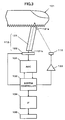
- Fig.3 is a schematic diagram for describing the operation of the fingerprint detection apparatus 100 according to an embodiment of the present invention.
- the fingerprint detection apparatus 100 has a circuit board 111 on which one or more light emitting diodes 112, an image obtaining part 113, and various electronic devices 114 are mounted and sealed with a sealing resin 115.
- the fingerprint detection apparatus 100 uses the light emitting diodes 112 (which are lit mainly for detecting a fingerprint of a finger 101) and the image obtaining part 113 to conducting a finger detection operation (hereinafter also referred to as "finger contact detection operation").
- the finger detection operation includes an operation of detecting a finger being in contact with the image obtaining part 113 and an operation of detecting a finger being in the vicinity of the image obtaining part.
- a fingerprint detection operation (fingerprint image obtaining operation) is conducted by the image obtaining part 113.
- the data of the detected fingerprint are output to an upper level apparatus. Therefore, the fingerprint detection apparatus 100 according to an embodiment of the present invention requires no other additional components for performing a finger detection operation. That is, with the fingerprint detection apparatus 100 according to an embodiment of the present invention, finger detection can be achieved by simply changing the control system.
- the light emitting diode 112 which is driven by a driver 133, emits light onto a finger 101 via the sealing resin 115.
- a resin material that blocks light may alternatively be used as the sealing resin 115.
- a block(s) of light transmitting resin may be embedded in the sealing resin 115 at an area between the light emitting diode 112 and a ceiling plane of the sealing resin 115.
- the light incident on the finger 101 diffuses in the finger and is directed to the image obtaining part 113.
- the image obtaining part 113 includes an image guide 121 and an image sensor 122.
- the image guide 121 includes plural optical fibers gathered and attached together.
- the image guide 121 having such a configuration is tilted to an angle of ⁇ degrees with respect to the circuit board 111.
- the planes on both ends (end planes) of the circuit board 111 are diced and polished so that end planes become parallel to the circuit board 111.
- first end plane 121a The light, which is incident on one end plane of the image guide 121 (hereinafter also referred to as "first end plane 121a") from an object having low refractive index (e.g., air), is not guided to the other end plane of the image guide 121 (hereinafter also referred to as “second end plane 121b"), but is instead reflected from the first end plane 121a.
- the light from the ridge points of the fingerprint is guided to the second end plane 121b and transmitted from the second plane 121b.
- the image guide 121 according to this embodiment of the present invention is tilted toward the lateral direction of the image sensor 122, the image guide 121 may be tilted toward the longitudinal direction of the image sensor 122.
- Fig.4 is a plane view of the image sensor 122 according to an embodiment of the present invention.
- the image sensor 122 has one or more imaging devices 142 arranged in a line on a semiconductor substrate 141.
- the image guide 121 and the image sensor 122 are positioned so that the direction in which the imaging devices 142 are arranged is in a manner substantially matching the longitudinal direction of the image guide 121.
- a system controller 132 controls operations of the image sensor 122 by generating sensor control signals and supplying the sensor control signals to the image sensor 122.
- the image sensor 122 converts the light transmitted from the second end plane 121b of the image guide 121 into electric signals (charges).
- the image sensor 122 supplies the converted electric signals as analog image signals to an analog/digital converter (ADC) 131.
- ADC analog/digital converter
- the analog image signals supplied from the image sensor 122 are converted into digital data (e.g., 8 bit digital data having 256 tones, 4 bit digital data having 16 tones) by the analog/digital converter 131.
- the digital data converted by the analog/digital converter 131 are supplied to the system controller 132.
- the system controller 132 processes (data processing) the digital data supplied from the analog/digital converter 131 and supplies the processed digital data to an interface circuit (IF) 134.
- the interface circuit 134 is connected to a host system (not shown) via a connector 135 for transferring the digital data processed by the system controller 132 to the host system.
- the connector 135 may be, for example, a BGA (Ball Grid Array) socket terminal often used in packaged integrated circuits or a solder connector such as lead frame terminal.
- the system controller 132 generates ADC control signals and supplies the generated ADC control signals to the analog/digital converter 131 for controlling operations of the analog/digital converter 131. Furthermore, the system controller 132 generates light control signals and supplies the generated light control signals to the driver 133 for driving and controlling the light emitting diodes 112.
- the system controller 132 in this embodiment of the present invention has two modes for operating (operation mode).
- one operation mode is a fingerprint image obtaining mode for enabling the image obtaining part 113 to obtain an image of a fingerprint of a finger
- the other operation mode is a finger detecting (finger contacting detecting) mode for enabling the image obtaining part to detect a finger being in contact with or in the vicinity of the image obtaining part 113.
- the system controller 132 may also have a complete system stop mode.
- the power consumption of the system controller 132 is substantially proportional to its clock (operating clock) and circuit scale. For example, in a case of operating in a finger contact detecting mode where low power consumption is desired, the system controller 132 is desired to operate with few circuits for reducing the clocks.
- a signal indicating the detection is used for switching the operation mode of the system controller 132.
- the signal may be used for communicating with the host system and allow the host system to control the system controller 132.
- the image sensor 122 is described with reference to Fig.5 .
- Fig.5 is a block diagram of the image sensor 122 according to an embodiment of the present invention.
- the image sensor 122 in this embodiment of the present invention includes an array of photodiodes 201 (photodiode array), an array of image transfer switches (image hold switches) 202 (image transfer switch array (image hold switch array)), an array of image storage devices 203 (image storage device array), and an image transfer interface 204.
- the photodiode array 201 is connected to the image storage device array 203 via the image transfer switch array 202.
- the image data stored in the image storage devices 203 are extracted from outside of the image sensor 122 via the image transfer interface 204.
- the electric charges stored in the photodiode array 201 by photoelectric conversion are transferred to the image storage device array 203 via the image transfer switch array 202 in accordance with image hold signals transmitted to the image transfer switch array 202 from the system controller 132.
- the transferred charges are extracted from outside of the image sensor 122 via the image transfer interface 204 in accordance with image transfer clocks from the system controller 132.
- Figs.6 and 7 are schematic diagrams for describing operations of the image sensor 122 according to an embodiment of the present invention. It is to be noted that Figs.6(A) and 7(A) indicate an image hold signal, Fig.6(B) indicates a charge stored in the image sensor 122, Fig.6(C) indicates a charge stored in the image storage device 203, Fig.6(D) indicates an image transfer clock, Figs.6(E) and 7(C) indicate an output signal, and Fig.7(B) indicates an LED control signal.
- a charge Q-1 stored in the photodiode array 201 is transferred to the image storage device array 203 with an image hold signal between the interval 1 and interval 2 as shown in Fig.6(A) .
- the transferred charge Q-1 is then transferred outside of the image sensor 122 during interval 2 by the image transfer clock as shown in Fig.6(D) .
- the light emitting diode 112 is lit on when an LED control signal of Fig.7(B) indicating "ON" is output in the interval 5 of Fig.7(A) .
- the charge stored in the photodiode array 201 in the interval 4 is output as a voltage proportional to the amount of charge with the output signal output in the interval 5 as shown in Fig.7(C) .
- the image signal output in this interval serves as background data when the light emitting diode 112 is not lit.
- the data output in the interval 6 are image data stored in the interval 5 and serve as image data when the light emitting diode 112 is lit.
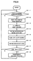
- Fig.8 is a flowchart showing an operation of the system controller 132 during finger contact detection according to an embodiment of the present invention.
- Step S1-1 After a predetermined period elapses (Step S1-1), the system controller 132 outputs an image hold signal in synchronization with a fingerprint detection pulse generated therein and waits until the next image hold signal (Step S1-2).
- the system controller 132 controls the driver 133 in synchronization with the image hold signal and lights (illuminate) the light emitting diode 112 (Step S1-3). Then, the system controller 132 reads an image and obtains digital data of the read out image by controlling the image sensor 122 and the analog/digital converter 131 (Step S1-4). In this step, the obtained digital data are background image data BK obtained by the imaging devices 142 positioned in the center or areas surrounding the center. The obtained image data in this step are image data obtained when the light emitting diode 112 is turned off.
- an added value or average value of the data of plural pixels may be used for noise removal.
- the pixels used for noise removal in this example are powers of two for simplifying the arithmetic circuit. Therefore, the pixels do not need to be powers of two depending on the circuit. It is however preferable to perform detection by using a small number of pixels for reducing power consumption.
- the system controller 132 After or during the obtaining of the background image data BK, the system controller 132 turns off the light emitting diode 112 by controlling the driver 133 (Step S1-5). The light emitting diode 112 is lit for a predetermined period. Then, the system controller 132, in synchronization with the image hold signal, reads an image and obtains digital data of the read out image by controlling the image sensor 122 and the analog/digital converter 131 (Step S1-6). For example, the obtained digital data are image data SG obtained by the imaging devices 142 positioned in the center or areas surrounding the center.
- the system controller 132 detects finger contact by determining whether (SG - BK) is greater than a threshold TH (Step S1-7).
- the threshold value may range from, for example, 10 to 100.
- the threshold value is low, the sensitivity for finger contact detection is high, and malfunction with respect to light disturbance (e.g., sunlight) tends to easily occur.
- the threshold value is high, the sensitivity for finger contact detection is low, and malfunction with respect to light disturbance hardly occurs. Accordingly, it is desired to set the value according to the environment in which the fingerprint detection apparatus is used.
- Step S1-7 the amount of light guided to the second end plane 121b of the image guide 121 increases when a finger is in contact with or in the vicinity of the first end plane 121a of the image guide 121. Accordingly, the system controller 132 determines detection of a finger being in contact with or in the vicinity of the first plane 121a of the image guide 121, to thereby initiate a fingerprint imaging process (fingerprint image obtaining process) (Step S1-8).
- Step S1-7 In a case where (SG - BK) is less than the threshold TH (No in Step S1-7), there is little difference (change) between the image data SG and the background data BK. Accordingly, the system controller 132 determines no detection of a finger being in contact with or in the vicinity of the first plane 121a of the image guide 121, to thereby return to Step S1-1 and continue the operation.
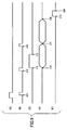
- Fig.9 is a timing chart during fingerprint detection according to an embodiment of the present invention.
- Fig.9(A) indicates a fingerprint detection pulse
- Fig.9(B) indicates an image hold signal
- Fig.9(C) indicates an illumination control signal
- Fig.9(D) indicates a data transfer timing
- Fig.9(E) indicates a finger contact determination signal.
- the system controller 132 In performing fingerprint detection after a predetermined period has elapsed in Step S1-1 of Fig.8 , the system controller 132 begins a regular image reading operation when the fingerprint detection pulse of Fig.9(A) rises, and generates an image hold signal of Fig.9(B) .
- the image sensor 122 receiving the image hold signal, resets the charge stored in the photodiode array 201 in synchronization with the rising pulse t11 of the image hold signal shown in Fig.9(B) and stores background image data (BK) in the photodiode array 201 during a period between pulse rising time t11 and the pulse rising time t12 of the next image hold signal.
- the background image data (BK) stored in the photodiode array 201 are transferred to the image storage device array 203 in synchronization with the pulse rise time t12 of the image hold signal. Then, the charge stored in the photodiode array 201 is reset.
- the system controller 132 outputs an illumination control signal that rises at a timing t13 for controlling the driver 133 to light the light emitting diode 112.
- the light of the light emitting diode 112 becomes incident on the finger 101 and is reflected to the image guide 121. Accordingly, the light from the image guide 121 incident on the image sensor 122 increases.
- the image sensor 122 converts the light into charges (photo-electric conversion) in correspondence with the fingerprint of the finger 101 and stores the charges therein.
- the illumination control signal in this example drops at the timing t15, to thereby turn off the light emitting diode 112.
- the period of lighting the light emitting diode 112 is set beforehand in the system controller 132 (in this example, from t13 to t15).
- the system controller 132 converts the charges stored in the image sensor 122 into voltage values from the timing t14 and allows voltage values to be supplied in the form of electric signals (analog signals) to the analog/digital converter 131 in synchronization with the image hold signal (system operation signal) of Fig.9(B) .
- the analog/digital converter (ADC) 131 converts the analog signals into digital image data.
- These digital image data are background image data (BK) stored in the image sensor 122 during the period between the pulse rise time t11 and the pulse rise time t12.
- electric signals corresponding to image data (SG) obtained by illumination by the light emitting diode 112 during the period between timing t17 and t18 are also supplied from the image sensor 122 to the analog/digital converter (ADC) 131.
- ADC analog/digital converter
- a single finger contact detection operation is conducted in three consecutive scanning intervals. That is, although a regular operation of obtaining an image of a fingerprint is performed consecutively as shown in the diagram of Fig.3 , the finger detection operation is intermittently conducted in a predetermined period (e.g., once every 100 milliseconds). Thereby, power consumption can be reduced significantly.
- the light emitting diodes 112 positioned in the surrounding areas need not to be lit up, but only the light emitting diode 112 positioned in the center is lit up. Thereby, power consumption of the light emitting diodes 112 can be reduced to approximately 1/3 compared to the power consumed during a fingerprint detection operation.
- an image is obtained by the imaging devices 142 only when a finger contacts the image guide 121. Nevertheless, depending on the surface roughness of the image guide 121 or the angle of the tilted optical fibers of the image guide 121, an image may be obtained without any contact simply by positioning a finger in the vicinity of the surface of the fingerprint detection apparatus 100.
- the image obtaining part 113 includes the image guide 121 and the image sensor 122, the image obtaining part 113 may be configured without using the image guide 121. With this configuration, the distance between the finger and the imaging devices 142 can be measured without being affected by disturbance light.
- the overall image can be acquired by laterally sliding a finger against the first plane 121a of the image guide 121.
- the image can be sufficiently obtained at a finger sliding rate of 42.3 cm/sec (42.3 ⁇ m (pixel pitch in 600 dpi) ⁇ 100 ⁇ seconds).
- the interval of the fingerprint detection pulse (scanning pulse) during a normal fingerprint detection ranges from 100 ⁇ m seconds to 400 ⁇ seconds.
- the fingerprint detection apparatus uses an image obtaining part for detecting a finger being in contact with or in the vicinity of the image obtaining part by referring to a difference between a image data signal (detection signal) and a background signal obtained when no finger is in the vicinity of the image obtaining part. Accordingly, with the above-described configuration and algorithm of the fingerprint detection apparatus of the present invention, a finger being contacting with or in the vicinity of the image obtaining part can be satisfactorily detected without having to use any additional component for finger detection.
Landscapes
- Engineering & Computer Science (AREA)
- Human Computer Interaction (AREA)
- Physics & Mathematics (AREA)
- General Physics & Mathematics (AREA)
- Multimedia (AREA)
- Theoretical Computer Science (AREA)
- Measurement Of The Respiration, Hearing Ability, Form, And Blood Characteristics Of Living Organisms (AREA)
- Image Input (AREA)
- Collating Specific Patterns (AREA)
Claims (4)
- Fingerabdruck-Detektiervorrichtung (100) zum Gewinnen eines Bildes eines Fingerabdrucks eines Fingers (101) durch Verwendung einer Lichtquelle (112) zur Abgabe eines Lichtes an den Finger und eines Bildgewinnungsteiles (113) zur Abgabe von elektrischen Signalen entsprechend empfangenem Licht,
dadurch gekennzeichnet,
dass die Fingerabdruck-Detektiervorrichtung (100) umfasst:eine System-Steuereinrichtung (132) zum Bestimmen, ob der Finger (101) mit dem Bildgewinnungsteil (113) in Kontakt ist oder sich in dessen Nähe befindet, durch Vergleichen eines Schwellenwertes mit einer Differenz zwischen einem Wert des elektrischen Signals, wenn die Lichtquelle (112) leuchtet, und einem Wert des elektrischen Signals, wenn die Lichtquelle (112) nicht leuchtet;wobei die System-Steuereinrichtung (132) dazu geeignet ist, den Schwellenwert auf einen von zumindest einem ersten Wert und einem zweiten Wert, welcher höher ist als der erste Wert, festzulegen,wobei die Empfindlichkeit zum Bestimmen eines Kontakts eines Fingers (101) geringer ist, wenn der Schwellenwert auf den zweiten Wert festgelegt ist, als dann, wenn der Schwellenwert auf den ersten Wert festgelegt ist. - Fingerabdruck-Detektiervorrichtung (100) nach Anspruch 1, wobei der Bildgewinnungsteil (113) eine Bild-Leiteinrichtung (121) zum Leiten des empfangenen Lichts und einen Bildsensor (122) zum Detektieren des von der Bild-Leiteinrichtung (121) geleiteten Lichtes enthält.
- Fingerabdruck-Detektiervorrichtung (100) nach Anspruch 1, wobei die System-Steuereinrichtung (132) intermittierend bzw. periodisch bestimmt, ob der Finger (101) mit dem Bildgewinnungsteil (113) in Kontakt ist oder sich in dessen Nähe befindet.
- Fingerabdruck-Detektiervorrichtung (100) nach Anspruch 1, wobei die System-Steuereinrichtung (132) von einem Finger-Detektiermodus in einen Fingerabdruck-Bildgewinnungsmodus umschaltet, wenn bestimmt wird, dass der Finger (101) mit dem Bildgewinnungsteil (113 in Kontakt ist oder sich in dessen Nähe befindet.
Applications Claiming Priority (1)
| Application Number | Priority Date | Filing Date | Title |
|---|---|---|---|
| JP2006228168A JP4162023B2 (ja) | 2006-08-24 | 2006-08-24 | 指紋検出装置 |
Publications (2)
| Publication Number | Publication Date |
|---|---|
| EP1892646A1 EP1892646A1 (de) | 2008-02-27 |
| EP1892646B1 true EP1892646B1 (de) | 2010-09-29 |
Family
ID=38543598
Family Applications (1)
| Application Number | Title | Priority Date | Filing Date |
|---|---|---|---|
| EP07252825A Expired - Fee Related EP1892646B1 (de) | 2006-08-24 | 2007-07-17 | Fingerabdruckerkennungsvorrichtung |
Country Status (5)
| Country | Link |
|---|---|
| US (1) | US8131025B2 (de) |
| EP (1) | EP1892646B1 (de) |
| JP (1) | JP4162023B2 (de) |
| CN (1) | CN101131732A (de) |
| DE (1) | DE602007009457D1 (de) |
Cited By (1)
| Publication number | Priority date | Publication date | Assignee | Title |
|---|---|---|---|---|
| CN108206809A (zh) * | 2016-12-16 | 2018-06-26 | 北京振兴计量测试研究所 | 一种涉密人员身份识别系统及方法 |
Families Citing this family (64)
| Publication number | Priority date | Publication date | Assignee | Title |
|---|---|---|---|---|
| US8358815B2 (en) * | 2004-04-16 | 2013-01-22 | Validity Sensors, Inc. | Method and apparatus for two-dimensional finger motion tracking and control |
| US8229184B2 (en) * | 2004-04-16 | 2012-07-24 | Validity Sensors, Inc. | Method and algorithm for accurate finger motion tracking |
| US8131026B2 (en) | 2004-04-16 | 2012-03-06 | Validity Sensors, Inc. | Method and apparatus for fingerprint image reconstruction |
| US8447077B2 (en) | 2006-09-11 | 2013-05-21 | Validity Sensors, Inc. | Method and apparatus for fingerprint motion tracking using an in-line array |
| US8175345B2 (en) | 2004-04-16 | 2012-05-08 | Validity Sensors, Inc. | Unitized ergonomic two-dimensional fingerprint motion tracking device and method |
| US8165355B2 (en) * | 2006-09-11 | 2012-04-24 | Validity Sensors, Inc. | Method and apparatus for fingerprint motion tracking using an in-line array for use in navigation applications |
| WO2005106774A2 (en) | 2004-04-23 | 2005-11-10 | Validity Sensors, Inc. | Methods and apparatus for acquiring a swiped fingerprint image |
| DE602005022900D1 (de) * | 2004-10-04 | 2010-09-23 | Validity Sensors Inc | Fingerabdruckerfassende konstruktionen mit einem substrat |
| US8107212B2 (en) * | 2007-04-30 | 2012-01-31 | Validity Sensors, Inc. | Apparatus and method for protecting fingerprint sensing circuitry from electrostatic discharge |
| US20110002461A1 (en) * | 2007-05-11 | 2011-01-06 | Validity Sensors, Inc. | Method and System for Electronically Securing an Electronic Biometric Device Using Physically Unclonable Functions |
| US8204281B2 (en) * | 2007-12-14 | 2012-06-19 | Validity Sensors, Inc. | System and method to remove artifacts from fingerprint sensor scans |
| US8276816B2 (en) * | 2007-12-14 | 2012-10-02 | Validity Sensors, Inc. | Smart card system with ergonomic fingerprint sensor and method of using |
| US8116540B2 (en) | 2008-04-04 | 2012-02-14 | Validity Sensors, Inc. | Apparatus and method for reducing noise in fingerprint sensing circuits |
| EP2321764A4 (de) * | 2008-07-22 | 2012-10-10 | Validity Sensors Inc | System, vorrichtung und verfahren zur sicherung einer gerätekomponente |
| US8391568B2 (en) * | 2008-11-10 | 2013-03-05 | Validity Sensors, Inc. | System and method for improved scanning of fingerprint edges |
| US8600122B2 (en) * | 2009-01-15 | 2013-12-03 | Validity Sensors, Inc. | Apparatus and method for culling substantially redundant data in fingerprint sensing circuits |
| US20100180136A1 (en) * | 2009-01-15 | 2010-07-15 | Validity Sensors, Inc. | Ultra Low Power Wake-On-Event Mode For Biometric Systems |
| US20100176892A1 (en) * | 2009-01-15 | 2010-07-15 | Validity Sensors, Inc. | Ultra Low Power Oscillator |
| US8278946B2 (en) | 2009-01-15 | 2012-10-02 | Validity Sensors, Inc. | Apparatus and method for detecting finger activity on a fingerprint sensor |
| US8487914B2 (en) * | 2009-06-18 | 2013-07-16 | Avago Technologies General Ip (Singapore) Pte. Ltd. | Optical fingerprint navigation device with light guide film |
| US8797298B2 (en) * | 2009-01-23 | 2014-08-05 | Avago Technologies General Ip (Singapore) Pte. Ltd. | Optical fingerprint navigation device with light guide film |
| US8374407B2 (en) | 2009-01-28 | 2013-02-12 | Validity Sensors, Inc. | Live finger detection |
| US20100208953A1 (en) * | 2009-02-17 | 2010-08-19 | Validity Sensors, Inc. | Illuminated Fingerprint Sensor and Method |
| US8188988B2 (en) * | 2009-05-12 | 2012-05-29 | Avago Technologies Ecbu Ip (Singapore) Pte. Ltd. | Finger navigation device |
| US8406487B2 (en) | 2009-09-16 | 2013-03-26 | General Electric Company | Method and system for contactless fingerprint detection and verification |
| US9336428B2 (en) | 2009-10-30 | 2016-05-10 | Synaptics Incorporated | Integrated fingerprint sensor and display |
| US9274553B2 (en) | 2009-10-30 | 2016-03-01 | Synaptics Incorporated | Fingerprint sensor and integratable electronic display |
| US9400911B2 (en) | 2009-10-30 | 2016-07-26 | Synaptics Incorporated | Fingerprint sensor and integratable electronic display |
| GB0921644D0 (en) * | 2009-12-10 | 2010-01-27 | St Microelectronics Res & Dev | Improvements in or relating to optical navigation devices |
| US8791792B2 (en) * | 2010-01-15 | 2014-07-29 | Idex Asa | Electronic imager using an impedance sensor grid array mounted on or about a switch and method of making |
| US8866347B2 (en) | 2010-01-15 | 2014-10-21 | Idex Asa | Biometric image sensing |
| US8421890B2 (en) | 2010-01-15 | 2013-04-16 | Picofield Technologies, Inc. | Electronic imager using an impedance sensor grid array and method of making |
| US9666635B2 (en) | 2010-02-19 | 2017-05-30 | Synaptics Incorporated | Fingerprint sensing circuit |
| US8716613B2 (en) * | 2010-03-02 | 2014-05-06 | Synaptics Incoporated | Apparatus and method for electrostatic discharge protection |
| US9001040B2 (en) | 2010-06-02 | 2015-04-07 | Synaptics Incorporated | Integrated fingerprint sensor and navigation device |
| US8331096B2 (en) | 2010-08-20 | 2012-12-11 | Validity Sensors, Inc. | Fingerprint acquisition expansion card apparatus |
| US8600123B2 (en) | 2010-09-24 | 2013-12-03 | General Electric Company | System and method for contactless multi-fingerprint collection |
| US8538097B2 (en) | 2011-01-26 | 2013-09-17 | Validity Sensors, Inc. | User input utilizing dual line scanner apparatus and method |
| US8594393B2 (en) | 2011-01-26 | 2013-11-26 | Validity Sensors | System for and method of image reconstruction with dual line scanner using line counts |
| GB2489100A (en) | 2011-03-16 | 2012-09-19 | Validity Sensors Inc | Wafer-level packaging for a fingerprint sensor |
| US8971588B2 (en) | 2011-03-30 | 2015-03-03 | General Electric Company | Apparatus and method for contactless high resolution handprint capture |
| US20130100043A1 (en) * | 2011-10-24 | 2013-04-25 | General Electric Company | Method for determining valid touch screen inputs |
| US10043052B2 (en) | 2011-10-27 | 2018-08-07 | Synaptics Incorporated | Electronic device packages and methods |
| US9195877B2 (en) | 2011-12-23 | 2015-11-24 | Synaptics Incorporated | Methods and devices for capacitive image sensing |
| US9785299B2 (en) | 2012-01-03 | 2017-10-10 | Synaptics Incorporated | Structures and manufacturing methods for glass covered electronic devices |
| US9137438B2 (en) | 2012-03-27 | 2015-09-15 | Synaptics Incorporated | Biometric object sensor and method |
| US9268991B2 (en) | 2012-03-27 | 2016-02-23 | Synaptics Incorporated | Method of and system for enrolling and matching biometric data |
| US9251329B2 (en) | 2012-03-27 | 2016-02-02 | Synaptics Incorporated | Button depress wakeup and wakeup strategy |
| US9600709B2 (en) | 2012-03-28 | 2017-03-21 | Synaptics Incorporated | Methods and systems for enrolling biometric data |
| US9152838B2 (en) | 2012-03-29 | 2015-10-06 | Synaptics Incorporated | Fingerprint sensor packagings and methods |
| WO2013155224A1 (en) | 2012-04-10 | 2013-10-17 | Picofield Technologies Inc. | Biometric sensing |
| US9665762B2 (en) | 2013-01-11 | 2017-05-30 | Synaptics Incorporated | Tiered wakeup strategy |
| CN103886297B (zh) * | 2014-03-26 | 2017-01-11 | 浙江大学 | 真假指纹的动态光学检测方法 |
| USD776664S1 (en) * | 2015-05-20 | 2017-01-17 | Chaya Coleena Hendrick | Smart card |
| KR101657005B1 (ko) * | 2015-06-11 | 2016-09-12 | 전문석 | 심전도 생체 인증 방법 |
| US9811708B2 (en) * | 2015-10-02 | 2017-11-07 | Fingerprint Cards Ab | Method and fingerprint sensing device with finger lost detection |
| CN105426876A (zh) * | 2015-12-22 | 2016-03-23 | 关仲泉 | 一种指纹读取装置及其控制模块 |
| KR101886035B1 (ko) * | 2017-06-08 | 2018-08-08 | 주식회사 센소니아 | 주변광의 영향을 감소시키는 지문 센싱 방법 |
| CN107247948A (zh) * | 2017-07-26 | 2017-10-13 | 苏州迈瑞微电子有限公司 | 一种接近程度检测装置和方法 |
| CN109670367A (zh) * | 2017-10-13 | 2019-04-23 | 深圳芯启航科技有限公司 | 一种光学图像传感系统 |
| WO2019071559A1 (zh) * | 2017-10-13 | 2019-04-18 | 深圳芯启航科技有限公司 | 一种光学图像传感系统 |
| CN107918768B (zh) * | 2017-11-28 | 2020-07-10 | Oppo广东移动通信有限公司 | 光学指纹识别方法、装置及电子设备 |
| CN109767714B (zh) * | 2019-03-08 | 2021-01-22 | 京东方科技集团股份有限公司 | 光电转换电路及其驱动方法、感光装置、显示装置 |
| KR20210132372A (ko) * | 2020-04-27 | 2021-11-04 | 삼성전자주식회사 | 광학적 객체 인식을 위한 참조 영상 획득 방법 및 이를 이용한 광학적 객체 인식 방법 |
Family Cites Families (6)
| Publication number | Priority date | Publication date | Assignee | Title |
|---|---|---|---|---|
| US5726443A (en) * | 1996-01-18 | 1998-03-10 | Chapman Glenn H | Vision system and proximity detector |
| US5781651A (en) | 1996-04-15 | 1998-07-14 | Aetex Biometric Corporation | Compact fingerprint recognizing apparatus illuminated with electroluminescent device |
| US6628377B1 (en) | 2000-04-04 | 2003-09-30 | Stmicroelectronics, Inc. | Scanning optical semiconductor fingerprint detector |
| JP2004021471A (ja) | 2002-06-14 | 2004-01-22 | Mitsubishi Electric Corp | 指紋照合装置 |
| JP4257221B2 (ja) | 2003-03-31 | 2009-04-22 | 東芝松下ディスプレイテクノロジー株式会社 | 表示装置および情報端末装置 |
| JP2005202694A (ja) | 2004-01-15 | 2005-07-28 | Mitsumi Electric Co Ltd | 検出装置 |
-
2006
- 2006-08-24 JP JP2006228168A patent/JP4162023B2/ja not_active Expired - Fee Related
-
2007
- 2007-06-11 CN CNA2007101091012A patent/CN101131732A/zh active Pending
- 2007-07-17 DE DE602007009457T patent/DE602007009457D1/de active Active
- 2007-07-17 US US11/778,769 patent/US8131025B2/en not_active Expired - Fee Related
- 2007-07-17 EP EP07252825A patent/EP1892646B1/de not_active Expired - Fee Related
Cited By (1)
| Publication number | Priority date | Publication date | Assignee | Title |
|---|---|---|---|---|
| CN108206809A (zh) * | 2016-12-16 | 2018-06-26 | 北京振兴计量测试研究所 | 一种涉密人员身份识别系统及方法 |
Also Published As
| Publication number | Publication date |
|---|---|
| EP1892646A1 (de) | 2008-02-27 |
| US20080049989A1 (en) | 2008-02-28 |
| JP2008048903A (ja) | 2008-03-06 |
| JP4162023B2 (ja) | 2008-10-08 |
| US8131025B2 (en) | 2012-03-06 |
| DE602007009457D1 (de) | 2010-11-11 |
| CN101131732A (zh) | 2008-02-27 |
Similar Documents
| Publication | Publication Date | Title |
|---|---|---|
| US8131025B2 (en) | Fingerprint detection apparatus | |
| US9103658B2 (en) | Optical navigation module with capacitive sensor | |
| CN100533252C (zh) | 图像捕获装置 | |
| TWI321287B (en) | Display device having optical input function | |
| US20100220900A1 (en) | Fingerprint sensing device | |
| EP1830123B1 (de) | Lichtleiterbauteil-Beleuchtungsvorrichtung und Bildaufnahmevorrichtung damit | |
| US8025519B2 (en) | Electro-optical reader with cable connector release | |
| US10732777B2 (en) | System and method for interference mitigation in a sensing device | |
| CN101398887A (zh) | 手指离开检测装置和方法及使用它的指纹读取装置和方法 | |
| KR20110121566A (ko) | 광학 핑거 내비게이션 장치, 광 가이드 조립체, 및 컴퓨터화 장치 | |
| JP2005295399A (ja) | タッチパネル入力装置 | |
| GB2353656A (en) | Hand held scanner having plural position detectors or navigators | |
| TW201502884A (zh) | 具有熱感應器之導航裝置 | |
| JP2008198130A (ja) | 画像読取装置、及び、画像読取方法、並びに、指紋読取装置 | |
| US20070291002A1 (en) | Laser mouse and control method thereof | |
| KR101872757B1 (ko) | 광학 센서 장치 및 광학 센싱 방법 | |
| KR101898067B1 (ko) | 광학 센서 모듈 및 광학 센싱 방법 | |
| US7701503B2 (en) | Method for controlling light source and optical input device using the same | |
| CN112800808A (zh) | 一种指纹识别方法和电子设备 | |
| CN105426876A (zh) | 一种指纹读取装置及其控制模块 | |
| KR20060076530A (ko) | 지문 인식 기능을 갖는 이동통신 단말기 | |
| US20070024586A1 (en) | Pen like optical mouse | |
| US20090294636A1 (en) | Optical movement detection device | |
| KR200182615Y1 (ko) | 초소형 광학 지문입력 장치 | |
| US8558818B1 (en) | Optical touch system with display screen |
Legal Events
| Date | Code | Title | Description |
|---|---|---|---|
| PUAI | Public reference made under article 153(3) epc to a published international application that has entered the european phase |
Free format text: ORIGINAL CODE: 0009012 |
|
| AK | Designated contracting states |
Kind code of ref document: A1 Designated state(s): AT BE BG CH CY CZ DE DK EE ES FI FR GB GR HU IE IS IT LI LT LU LV MC MT NL PL PT RO SE SI SK TR |
|
| AX | Request for extension of the european patent |
Extension state: AL BA HR MK YU |
|
| 17P | Request for examination filed |
Effective date: 20080424 |
|
| AKX | Designation fees paid |
Designated state(s): DE FR GB |
|
| 17Q | First examination report despatched |
Effective date: 20090205 |
|
| GRAP | Despatch of communication of intention to grant a patent |
Free format text: ORIGINAL CODE: EPIDOSNIGR1 |
|
| GRAS | Grant fee paid |
Free format text: ORIGINAL CODE: EPIDOSNIGR3 |
|
| GRAA | (expected) grant |
Free format text: ORIGINAL CODE: 0009210 |
|
| AK | Designated contracting states |
Kind code of ref document: B1 Designated state(s): DE FR GB |
|
| REG | Reference to a national code |
Ref country code: GB Ref legal event code: FG4D |
|
| REF | Corresponds to: |
Ref document number: 602007009457 Country of ref document: DE Date of ref document: 20101111 Kind code of ref document: P |
|
| PLBE | No opposition filed within time limit |
Free format text: ORIGINAL CODE: 0009261 |
|
| STAA | Information on the status of an ep patent application or granted ep patent |
Free format text: STATUS: NO OPPOSITION FILED WITHIN TIME LIMIT |
|
| PGFP | Annual fee paid to national office [announced via postgrant information from national office to epo] |
Ref country code: GB Payment date: 20110613 Year of fee payment: 5 |
|
| REG | Reference to a national code |
Ref country code: DE Ref legal event code: R097 Ref document number: 602007009457 Country of ref document: DE Effective date: 20110630 |
|
| PGFP | Annual fee paid to national office [announced via postgrant information from national office to epo] |
Ref country code: FR Payment date: 20110729 Year of fee payment: 5 |
|
| PGFP | Annual fee paid to national office [announced via postgrant information from national office to epo] |
Ref country code: DE Payment date: 20110722 Year of fee payment: 5 |
|
| GBPC | Gb: european patent ceased through non-payment of renewal fee |
Effective date: 20120717 |
|
| REG | Reference to a national code |
Ref country code: FR Ref legal event code: ST Effective date: 20130329 |
|
| PG25 | Lapsed in a contracting state [announced via postgrant information from national office to epo] |
Ref country code: GB Free format text: LAPSE BECAUSE OF NON-PAYMENT OF DUE FEES Effective date: 20120717 Ref country code: DE Free format text: LAPSE BECAUSE OF NON-PAYMENT OF DUE FEES Effective date: 20130201 Ref country code: FR Free format text: LAPSE BECAUSE OF NON-PAYMENT OF DUE FEES Effective date: 20120731 |
|
| REG | Reference to a national code |
Ref country code: DE Ref legal event code: R119 Ref document number: 602007009457 Country of ref document: DE Effective date: 20130201 |