EP1892459B1 - Lighting device for a liquid crystal display device - Google Patents
Lighting device for a liquid crystal display device Download PDFInfo
- Publication number
- EP1892459B1 EP1892459B1 EP06731034A EP06731034A EP1892459B1 EP 1892459 B1 EP1892459 B1 EP 1892459B1 EP 06731034 A EP06731034 A EP 06731034A EP 06731034 A EP06731034 A EP 06731034A EP 1892459 B1 EP1892459 B1 EP 1892459B1
- Authority
- EP
- European Patent Office
- Prior art keywords
- light
- illumination light
- crystal display
- emitting
- illumination
- Prior art date
- Legal status (The legal status is an assumption and is not a legal conclusion. Google has not performed a legal analysis and makes no representation as to the accuracy of the status listed.)
- Ceased
Links
- 239000004973 liquid crystal related substance Substances 0.000 title description 31
- 238000005286 illumination Methods 0.000 claims description 52
- 230000003287 optical effect Effects 0.000 claims description 21
- 239000000463 material Substances 0.000 claims description 14
- 239000011347 resin Substances 0.000 description 8
- 229920005989 resin Polymers 0.000 description 8
- 239000011521 glass Substances 0.000 description 4
- 229920000515 polycarbonate Polymers 0.000 description 4
- 239000004417 polycarbonate Substances 0.000 description 4
- 238000009792 diffusion process Methods 0.000 description 3
- JNDMLEXHDPKVFC-UHFFFAOYSA-N aluminum;oxygen(2-);yttrium(3+) Chemical compound [O-2].[O-2].[O-2].[Al+3].[Y+3] JNDMLEXHDPKVFC-UHFFFAOYSA-N 0.000 description 2
- 238000012856 packing Methods 0.000 description 2
- 229910019901 yttrium aluminum garnet Inorganic materials 0.000 description 2
- -1 acryl Chemical group 0.000 description 1
- 239000002390 adhesive tape Substances 0.000 description 1
- 229910052782 aluminium Inorganic materials 0.000 description 1
- XAGFODPZIPBFFR-UHFFFAOYSA-N aluminium Chemical compound [Al] XAGFODPZIPBFFR-UHFFFAOYSA-N 0.000 description 1
- 230000000295 complement effect Effects 0.000 description 1
- 239000000428 dust Substances 0.000 description 1
- 230000000694 effects Effects 0.000 description 1
- 238000001704 evaporation Methods 0.000 description 1
- 229910052751 metal Inorganic materials 0.000 description 1
- 239000002184 metal Substances 0.000 description 1
- 229920002379 silicone rubber Polymers 0.000 description 1
- 239000004945 silicone rubber Substances 0.000 description 1
- 239000000758 substrate Substances 0.000 description 1
Images


Classifications
-
- G—PHYSICS
- G02—OPTICS
- G02B—OPTICAL ELEMENTS, SYSTEMS OR APPARATUS
- G02B27/00—Optical systems or apparatus not provided for by any of the groups G02B1/00 - G02B26/00, G02B30/00
- G02B27/01—Head-up displays
- G02B27/0101—Head-up displays characterised by optical features
-
- G—PHYSICS
- G02—OPTICS
- G02F—OPTICAL DEVICES OR ARRANGEMENTS FOR THE CONTROL OF LIGHT BY MODIFICATION OF THE OPTICAL PROPERTIES OF THE MEDIA OF THE ELEMENTS INVOLVED THEREIN; NON-LINEAR OPTICS; FREQUENCY-CHANGING OF LIGHT; OPTICAL LOGIC ELEMENTS; OPTICAL ANALOGUE/DIGITAL CONVERTERS
- G02F1/00—Devices or arrangements for the control of the intensity, colour, phase, polarisation or direction of light arriving from an independent light source, e.g. switching, gating or modulating; Non-linear optics
- G02F1/01—Devices or arrangements for the control of the intensity, colour, phase, polarisation or direction of light arriving from an independent light source, e.g. switching, gating or modulating; Non-linear optics for the control of the intensity, phase, polarisation or colour
- G02F1/13—Devices or arrangements for the control of the intensity, colour, phase, polarisation or direction of light arriving from an independent light source, e.g. switching, gating or modulating; Non-linear optics for the control of the intensity, phase, polarisation or colour based on liquid crystals, e.g. single liquid crystal display cells
- G02F1/133—Constructional arrangements; Operation of liquid crystal cells; Circuit arrangements
- G02F1/1333—Constructional arrangements; Manufacturing methods
- G02F1/1335—Structural association of cells with optical devices, e.g. polarisers or reflectors
- G02F1/1336—Illuminating devices
- G02F1/133602—Direct backlight
- G02F1/133603—Direct backlight with LEDs
-
- G—PHYSICS
- G02—OPTICS
- G02B—OPTICAL ELEMENTS, SYSTEMS OR APPARATUS
- G02B27/00—Optical systems or apparatus not provided for by any of the groups G02B1/00 - G02B26/00, G02B30/00
- G02B27/01—Head-up displays
- G02B27/0101—Head-up displays characterised by optical features
- G02B2027/0112—Head-up displays characterised by optical features comprising device for genereting colour display
-
- G—PHYSICS
- G02—OPTICS
- G02F—OPTICAL DEVICES OR ARRANGEMENTS FOR THE CONTROL OF LIGHT BY MODIFICATION OF THE OPTICAL PROPERTIES OF THE MEDIA OF THE ELEMENTS INVOLVED THEREIN; NON-LINEAR OPTICS; FREQUENCY-CHANGING OF LIGHT; OPTICAL LOGIC ELEMENTS; OPTICAL ANALOGUE/DIGITAL CONVERTERS
- G02F1/00—Devices or arrangements for the control of the intensity, colour, phase, polarisation or direction of light arriving from an independent light source, e.g. switching, gating or modulating; Non-linear optics
- G02F1/01—Devices or arrangements for the control of the intensity, colour, phase, polarisation or direction of light arriving from an independent light source, e.g. switching, gating or modulating; Non-linear optics for the control of the intensity, phase, polarisation or colour
- G02F1/13—Devices or arrangements for the control of the intensity, colour, phase, polarisation or direction of light arriving from an independent light source, e.g. switching, gating or modulating; Non-linear optics for the control of the intensity, phase, polarisation or colour based on liquid crystals, e.g. single liquid crystal display cells
- G02F1/133—Constructional arrangements; Operation of liquid crystal cells; Circuit arrangements
- G02F1/1333—Constructional arrangements; Manufacturing methods
- G02F1/1335—Structural association of cells with optical devices, e.g. polarisers or reflectors
- G02F1/1336—Illuminating devices
- G02F1/133602—Direct backlight
- G02F1/133606—Direct backlight including a specially adapted diffusing, scattering or light controlling members
- G02F1/133607—Direct backlight including a specially adapted diffusing, scattering or light controlling members the light controlling member including light directing or refracting elements, e.g. prisms or lenses
-
- H—ELECTRICITY
- H10—SEMICONDUCTOR DEVICES; ELECTRIC SOLID-STATE DEVICES NOT OTHERWISE PROVIDED FOR
- H10H—INORGANIC LIGHT-EMITTING SEMICONDUCTOR DEVICES HAVING POTENTIAL BARRIERS
- H10H20/00—Individual inorganic light-emitting semiconductor devices having potential barriers, e.g. light-emitting diodes [LED]
- H10H20/80—Constructional details
- H10H20/85—Packages
- H10H20/855—Optical field-shaping means, e.g. lenses
Definitions
- the present invention relates to an illuminating device and liquid-crystal display panel having light-emitting elements, such as light-emitting diodes, and to a liquid-crystal display apparatus having illumination means for illuminating the liquid-crystal panel transmissively.
- Patent Document 1 Japanese Unexamined Patent Application No. 2003-295105
- the liquid-crystal display apparatus 4 has a liquid-crystal display panel 6 and light-emitting elements 7, 8, such as light-emitting diodes, that illuminates the liquid-crystal panel 6 transmissively.
- the light-emitting elements 7, 8 each have a base 7a, 8a, a light-emitting diode chip 7c, 8c provided in a recess 7b, 8b formed in the base 7a, 8a, a fluorescent material 7d, 8d such as of YAG (Yttrium Aluminum Garnet) for wavelength-converting the light emitted by the light-emitting diode chip 7c, 8c, and a lens 7e, 8e formed of a light-transmissive resin in a generally semispherical form (see Fig.
- the light-emitting diode chip 7c, 8c is to emit blue light while the fluorescent material 7d, 8d is to convert part of the light emitted from the light-emitting diode chip 7c, 8c into yellow, a complementary color of blue.
- the beams of illumination light L1, L2, emitted by the light-emitting elements 7, 8, are mixed with the blue emitted by the light-emitting diodes chip 7c, 8c and with the yellow converted by the fluorescent materials 7d, 8d, thus being turned into generally white in color.
- the beams of illumination light L1, L2, emitted by the light-emitting diodes 7, 8, have a light portion Lw white in color at a center whereas a light portion Ly obliquely emitted by the light-emitting diodes 7, 8 is somewhat yellowish.
- the passage length D1 the light obliquely emitted from the light-emitting diode chips 7c, 8c passes through the fluorescent materials 7d, 8d, is greater than the length D2 the light emitted nearly parallel with the optical axis passes through the fluorescent material 7d.
- the obliquely emitted portion of light is in a color somewhat yellowish.
- the present invention has been made in view of the problem and is to provide an illuminating device that possibly causes less irregularity of color.
- the present invention comprises, as described in claim 1, a first light-emitting element 23 for emitting a first illuminating light L1, a second light-emitting element 24 provided juxtaposed with the first light-emitting element 23 and for emitting a second illuminating light L2, and an optical member 26 formed of a light-transmissive material and having a first slant surface 26a for refracting the first beam of illumination light L1 and a second slant surface 26b for refracting the second beam of illumination light L2 in a manner overlapping part of the first beam of illumination light L1 and part of the second beam of illumination light L2 together.
- the optical member 26 has a first incident surface 26a formed by the first slant surface on which the first beam of illumination light L1 is to be incident, a first exit surface 26c formed by a convex lens surface through which the first beam of illumination light L1 is to exit, a second incident surface 26b formed by the second slant surface on which the second beam of illumination light L2 is to be incident and a second exit surface 26d, 55d formed by a convex lens surface through which the second beam of illumination light L2 is to exit.
- the first light-emitting element 23 and the second light-emitting element 24 each have a light-emitting diode chip 23c, 24c and a fluorescent body 23d, 24d for wavelength-converting the beam of light emitted by the light-emitting diode chip 23c, 24c, as described in claim 2.
- a circuit board 25 is provided which is mounted with a plurality of the first light-emitting elements 23 and a plurality of the second light-emitting elements 24, as described in claim 3.
- FIG. 1 to 5 show the embodiment.
- a head-up display 11 is arranged in a dashboard 12 of a vehicle (see Fig. 2 ).
- the display light L, projected by the head-up display 11, is reflected by a front glass 13 toward an observer 14.
- the observer 14 is allowed to view a virtual image V superposed on a scene.
- the head-up display 11 contains a liquid-crystal display apparatus 15 and a reflector 16 in its housing 17.
- the liquid-crystal display apparatus 15 has a liquid-crystal display panel 19, a light-diffusion plate 20, illumination means 21 and a case 22.
- the liquid-crystal display panel 19 is bonded with polarizer films at front and rear surfaces of a liquid-crystal cell that a liquid crystal is filled between a pair of glass substrates formed with transparent electrodes, thus being fixed on the case 22.
- the light diffusion plate 20 is arranged on a backside of the liquid-crystal display panel 19 and fixed on the case 22.
- the illumination means 21 has a light-emitting diode 23 (first light-emitting element), a light-emitting diode 24 (second light-emitting element), a circuit board 25 and an optical element 26.
- the illumination means 21 is arranged in back of the liquid-crystal display panel 19 and for illuminating the liquid-crystal display panel 19 transmissively.
- the case 22 is formed in a nearly rectangularly cylindrical form so that the liquid-crystal display panel 19 and the light diffusion plate 20 are held at the front end of the case 21.
- the case 22 has a rear end fixed on a heat sink member, referred later.
- the reflector 16 has a concave mirror 30, a support member 31 and a stepping motor 32.
- the concave mirror 30 has a reflection surface 30a formed by evaporating a metal (e.g. aluminum) over a resin (e.g. polycarbonate).
- the reflection surface 30a is made as a concave surface so that a virtual image V can be displayed by enlarging the display light L caused by the liquid-crystal display apparatus 15.
- the concave mirror 30 is bonded on the support member 31 by means of a double-sided adhesive tape.
- the support member 31 is formed of a resin (e.g. ABS) and integral with a gear 34 and a shaft 35.
- the shaft 35 of the support member 31 is pivotally supported by the housing 17.
- a gear 37 is attached on the rotary shaft of the stepping motor 32.
- the gear 37 is in mesh with the gear 34 of the support member 31.
- the concave mirror 30 is supported rotatably together with the support member 31.
- the stepping motor 32 can rotate the concave mirror 30, to adjust the projecting direction of display light L.
- the observer 14 is to operate a push button switch (not shown) and adjust the angle of the concave mirror 30 so that display light L can be reflected to the position of the eye (i.e. so that a virtual image V can be visually perceived).
- the heat sink member 40 is a heat sink member, which heat sink member 40 is arranged in an opening 17a of the housing 17.
- the heat sink member 40 at its flange 40a is fixed on the housing 17 by means of not-shown screws.
- the heat sink member 40 is for releasing the heat of the light-emitting diodes 23, 24 to the outside of the housing 17 through a heat conductive sheet 41 formed of an elastic body, such as of silicone rubber.
- the heat sink member 40 has a multiplicity of plate-like fins 40b.
- the heat sink member 40 is formed with a convex 40c in a rectangular parallelepiped form.
- the heat conductive sheet 41 has a concave 41a corresponding to the convex 40c of the heat sink member 40, thus increasing the contact area of between the heat conductive sheet 41 and the heat sink member 40.
- 42 is a packing member in a rectangular annular form, which packing member 42 closes between the heat sink member 40 and the opening 17a of the housing 17, thereby preventing the intrusion of dust into the housing 17.
- the housing 17 accommodates therein the liquid-crystal display apparatus 15 and the reflector 16.
- the housing 17 is provided with a window 44 allowing display light L to exit.
- the window 44 is formed of a light-transmissive resin (e.g. acryl) and made in a curved form.
- the housing 17 is provided with a light-shield wall 17c, thus preventing the phenomenon (washout) that ambient light, such as solar light, enters the liquid-crystal display apparatus 15 and makes it not easy to view the virtual image V.
- the light-shield wall 17c is in a plate form and formed obliquely extending downwardly from the upper part of the housing 17.
- the illumination means 21 having the light-emitting diodes 23, 24, the circuit board 25 and the optical member 26 each have a base 23a, 24a, a light-emitting diode chip 23c, 24c, a yellow fluorescent material 23d, 24d for waveform-converting the light emitted from the light-emitting diode chip 23c, 24c, and a lens made of a light-transmissive resin.
- the light-emitting diode chip 23c, 24c are to emit blue light while the fluorescent material 23d, 24d is to convert part of the light emitted by the light-emitting diode chip 23c, 24c into yellow.
- the beams of illumination light L1, L2 emitted from the light-emitted diodes 23, 24, are immixed with the blue emitted by the light-emitting diode chip 23c, 24c and with the yellow converted by the fluorescent material 23d, 24d, thus being changed into nearly white in color.
- the light-emitting diodes 23, 24 are juxtaposed four on each (totally eight) on the circuit board 24 (see Fig. 4 ).
- a wiring pattern (not shown) is provided to supply power to the light-emitting diodes 23, 24.
- the optical member 26 formed of a light-transmissive resin such as polycarbonate, has a first slant surface 26a upon which is to be incident the first beam of illumination light L1 emitted by the light-emitting diode 23, a second slant surface 26b upon which is to be incident the second beam of illumination light L2 emitted by the light-emitting diode 24, a convex lens surface 26c allowing the first beam of illumination light L1 to exit, and a convex lens surface 26d allowing the second beam of illumination light L2 to exit.
- the first and second slant surfaces 26a, 26b of the optical member 26, are finished as flat surfaces while the convex lens surfaces 26c, 26d are as spherical surfaces.
- the first beam of illumination light L1, emitted by the light-emitting diode 23, is refracted at the first slant surface 26a and incident upon the optical member 26, and further refracted at the convex lens 26c and allowed to exit from the optical member 26, thus illuminated to the liquid-crystal display panel 19.
- the second beam of illumination light L2, emitted by the light-emitting diode 24, is refracted at the second slant surface 26b and incident upon the optical member 26, and further refracted at the convex lens 26d and allowed to exit from the optical member 26, thus illuminated Lo the liquid-crystal display panel 19.
- Fig. 6 shows an example wich is not part of the claimed invention. It is different only in respect of its optical members 55, 56 wherein the other structures are similar to the embodiment.
- the optical member 55 is formed of a light-transmissive resin, such as polycarbonate. This has an incident surface 55a upon which are to be incident the first beam of illumination light L1 and the second beam of illumination light L2 that are emitted by the light-emitting diodes 23, 24, a convex lens surface 55c through which the first beam of illumination light L1 is to exit, and a convex lens surface 55d through which the second beam of illumination light L2 is to exit.
- the optical member 56 is formed of a light-transmissive resin, such as polycarbonate. This has a first slant surface 56a upon which the first beam of illumination light L1 exited from the convex lens surface 55c is to be incident, a second slant surface 56b upon which the second beam of illumination light L2 exited from the convex lens surface 55d is to be incident, and an exit surface 56c through which the first beam of illumination light L1 and second beam of illumination light L2 is to exit.
- a light-transmissive resin such as polycarbonate
- the first beam of illumination light L1, emitted by the light-emitting diode 23, is refracted at the incident surface 55a, the convex lens surface 55c and the first slant surface 56a, and allowed to exit through the exit surface 56c and illuminated to the liquid-crystal display panel 19.
- the second beam of illumination light L2, emitted by the light-emitting diode 24, is refracted at the incident surface 55a, the convex lens surface 55d and the second slant surface 56b, and allowed to exit through the exit surface 56c and illuminated to the liquid-crystal display panel 19.
- the first beam of illumination light L1 and the second beam of illumination light L2, that are obliquely illuminated by the light-emitting diodes 23, 24, are partly in a color somewhat yellowish but is less in color irregularity because those overlap with white portions of the second and first illumination light L2, L1 that are illuminated nearly parallel with the optical axis by the light-emitting diodes 24, 23.
- the present invention is applicable to a liquid-crystal display apparatus having illumination means for illuminating a liquid-crystal display panel transmissively.
Landscapes
- Physics & Mathematics (AREA)
- Nonlinear Science (AREA)
- General Physics & Mathematics (AREA)
- Optics & Photonics (AREA)
- Mathematical Physics (AREA)
- Chemical & Material Sciences (AREA)
- Crystallography & Structural Chemistry (AREA)
- Liquid Crystal (AREA)
- Fittings On The Vehicle Exterior For Carrying Loads, And Devices For Holding Or Mounting Articles (AREA)
- Instrument Panels (AREA)
- Led Device Packages (AREA)
Description
- The present invention relates to an illuminating device and liquid-crystal display panel having light-emitting elements, such as light-emitting diodes, and to a liquid-crystal display apparatus having illumination means for illuminating the liquid-crystal panel transmissively.
- Traditionally, a variety of vehicular head-up displays, using liquid-crystal display apparatuses, have been proposed and disclosed in
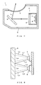
Patent Document 1, for example. Such a vehicular head-up display 1 is to project display light L onto a vehicular front glass or a translucent plate called combiner and display a virtual image. A vehicular head-up display 1 contains a liquid-crystal display apparatus 4 and a reflection mirror 5, in ahousing 3 having a light-transmissive window 2. The display light L, emitted by the liquid-crystal display apparatus 4, is reflected by the reflection mirror 5 and projected onto the front glass or the translucent plate (seeFig. 7 ).
Patent Document 1: Japanese Unexamined Patent Application No.2003-295105 - The liquid-
crystal display apparatus 4 has a liquid-crystal display panel 6 and light-emittingelements crystal panel 6 transmissively. The light-emittingelements diode chip 7c, 8c provided in arecess fluorescent material diode chip 7c, 8c, and alens 7e, 8e formed of a light-transmissive resin in a generally semispherical form (seeFig. 9 ). The light-emittingdiode chip 7c, 8c is to emit blue light while thefluorescent material diode chip 7c, 8c into yellow, a complementary color of blue. The beams of illumination light L1, L2, emitted by the light-emittingelements diodes chip 7c, 8c and with the yellow converted by thefluorescent materials - Japanese patent application nos.
2001-135121 2000-261034 - However, the beams of illumination light L1, L2, emitted by the light-emitting
diodes diodes crystal display panel 6 being illuminated transmissively with the beams of illumination light L1, L2. This problem can be considered because of the reason that the beams of light, emitted by the light-emittingdiode chips 7c, 8c, are different in passage length through thefluorescent materials diode chips 7c, 8c passes through thefluorescent materials fluorescent material 7d. Thus, the obliquely emitted portion of light is in a color somewhat yellowish.
The present invention has been made in view of the problem and is to provide an illuminating device that possibly causes less irregularity of color. - The present invention comprises, as described in
claim 1, a first light-emittingelement 23 for emitting a first illuminating light L1, a second light-emittingelement 24 provided juxtaposed with the first light-emittingelement 23 and for emitting a second illuminating light L2, and anoptical member 26 formed of a light-transmissive material and having afirst slant surface 26a for refracting the first beam of illumination light L1 and asecond slant surface 26b for refracting the second beam of illumination light L2 in a manner overlapping part of the first beam of illumination light L1 and part of the second beam of illumination light L2 together. Theoptical member 26 has afirst incident surface 26a formed by the first slant surface on which the first beam of illumination light L1 is to be incident, afirst exit surface 26c formed by a convex lens surface through which the first beam of illumination light L1 is to exit, asecond incident surface 26b formed by the second slant surface on which the second beam of illumination light L2 is to be incident and asecond exit surface - Meanwhile, in the invention, the first light-emitting
element 23 and the second light-emittingelement 24 each have a light-emittingdiode chip fluorescent body diode chip claim 2. - Meanwhile, in the invention, a
circuit board 25 is provided which is mounted with a plurality of the first light-emittingelements 23 and a plurality of the second light-emitting elements 24, as described inclaim 3. - By overlapping part of the first beam of illumination light emitted from the first light-emitting element and part of the second beam of illumination light emitted from the second light-emitting element together, the possibility of color irregularity occurrence can be reduced.
-
- [
Fig. 1 ] A sectional view showing an embodiment of the present invention. - [
Fig. 2 ] An overview of a head-up display showing the embodiment. - [
Fig. 3 ] A magnifying sectional view of illuminating means showing the embodiment. - [
Fig. 4 ] A front view of a circuit board showing the embodiment. - [
Fig. 5 ] A sectional view of illuminating means showing the embodiment. - [
Fig. 6 ] A sectional view showing an example. - [
Fig. 7 ] A sectional view showing a prior art. - [
Fig. 8 ] A magnifying sectional view of a light-emitting diode showing the prior art. - [
Fig. 9 ] A sectional view showing the prior art. -
- 19
- Liquid-crystal display panel
- 21
- Illuminating means
- 23
- Light-emitting diode (first light-emitting element)
- 23c
- Light-emitting diode chip
- 23d
- Fluorescent material
- 24c
- Light-emitting diode chip
- 24d
- Fluorescent material
- 25
- Circuit board
- 26
- Optical member
- 26a
- First slant surface (first incident surface)
- 26b
- Second slant surface (second incident surface)
- 26c
- Convex lens surface (first exit surface)
- 26d
- Convex lens surface (second exit surface)
- 55c
- Convex lens surface (first exit surface)
- 55d
- Convex lens surface (second exit surface)
- 56
- Optical member
- 56a
- First slant surface (first incident surface)
- 56b
- Second slant surface (second incident surface)
- L1
- First beam of illumination light
- L2
- Second beam of illumination light
- Based on the attached drawings, explanation will be made below on one embodiment the invention is applied to a head-up display.
Figs. 1 to 5 show the embodiment. - A head-up
display 11 is arranged in adashboard 12 of a vehicle (seeFig. 2 ). The display light L, projected by the head-updisplay 11, is reflected by afront glass 13 toward anobserver 14. Theobserver 14 is allowed to view a virtual image V superposed on a scene. - The head-up
display 11 contains a liquid-crystal display apparatus 15 and areflector 16 in itshousing 17. The liquid-crystal display apparatus 15 has a liquid-crystal display panel 19, a light-diffusion plate 20, illumination means 21 and acase 22.
The liquid-crystal display panel 19 is bonded with polarizer films at front and rear surfaces of a liquid-crystal cell that a liquid crystal is filled between a pair of glass substrates formed with transparent electrodes, thus being fixed on thecase 22. Thelight diffusion plate 20 is arranged on a backside of the liquid-crystal display panel 19 and fixed on thecase 22. - The illumination means 21 has a light-emitting diode 23 (first light-emitting element), a light-emitting diode 24 (second light-emitting element), a
circuit board 25 and anoptical element 26. The illumination means 21 is arranged in back of the liquid-crystal display panel 19 and for illuminating the liquid-crystal display panel 19 transmissively.
Thecase 22 is formed in a nearly rectangularly cylindrical form so that the liquid-crystal display panel 19 and thelight diffusion plate 20 are held at the front end of thecase 21. Thecase 22 has a rear end fixed on a heat sink member, referred later. - The
reflector 16 has aconcave mirror 30, asupport member 31 and a steppingmotor 32. Theconcave mirror 30 has areflection surface 30a formed by evaporating a metal (e.g. aluminum) over a resin (e.g. polycarbonate). Thereflection surface 30a is made as a concave surface so that a virtual image V can be displayed by enlarging the display light L caused by the liquid-crystal display apparatus 15. Theconcave mirror 30 is bonded on thesupport member 31 by means of a double-sided adhesive tape. Thesupport member 31 is formed of a resin (e.g. ABS) and integral with agear 34 and ashaft 35. Theshaft 35 of thesupport member 31 is pivotally supported by thehousing 17. - A
gear 37 is attached on the rotary shaft of the steppingmotor 32. Thegear 37 is in mesh with thegear 34 of thesupport member 31. Theconcave mirror 30 is supported rotatably together with thesupport member 31. The steppingmotor 32 can rotate theconcave mirror 30, to adjust the projecting direction of display light L. Theobserver 14 is to operate a push button switch (not shown) and adjust the angle of theconcave mirror 30 so that display light L can be reflected to the position of the eye (i.e. so that a virtual image V can be visually perceived). - 40 is a heat sink member, which
heat sink member 40 is arranged in an opening 17a of thehousing 17. Theheat sink member 40 at itsflange 40a is fixed on thehousing 17 by means of not-shown screws. Theheat sink member 40 is for releasing the heat of the light-emittingdiodes housing 17 through a heatconductive sheet 41 formed of an elastic body, such as of silicone rubber. Theheat sink member 40 has a multiplicity of plate-like fins 40b. Theheat sink member 40 is formed with a convex 40c in a rectangular parallelepiped form. The heatconductive sheet 41 has a concave 41a corresponding to the convex 40c of theheat sink member 40, thus increasing the contact area of between the heatconductive sheet 41 and theheat sink member 40. 42 is a packing member in a rectangular annular form, which packingmember 42 closes between theheat sink member 40 and the opening 17a of thehousing 17, thereby preventing the intrusion of dust into thehousing 17. - The
housing 17 accommodates therein the liquid-crystal display apparatus 15 and thereflector 16. Thehousing 17 is provided with awindow 44 allowing display light L to exit. Thewindow 44 is formed of a light-transmissive resin (e.g. acryl) and made in a curved form. Thehousing 17 is provided with a light-shield wall 17c, thus preventing the phenomenon (washout) that ambient light, such as solar light, enters the liquid-crystal display apparatus 15 and makes it not easy to view the virtual image V. The light-shield wall 17c is in a plate form and formed obliquely extending downwardly from the upper part of thehousing 17. - Next, description is made in detail on the illumination means 21 having the light-emitting
diodes circuit board 25 and theoptical member 26.
As shown inFig. 3 , the light-emittingdiodes base diode chip yellow fluorescent material diode chip diode chip fluorescent material diode chip diodes diode chip fluorescent material diodes Fig. 4 ). On thecircuit board 25, a wiring pattern (not shown) is provided to supply power to the light-emittingdiodes - The
optical member 26, formed of a light-transmissive resin such as polycarbonate, has afirst slant surface 26a upon which is to be incident the first beam of illumination light L1 emitted by the light-emittingdiode 23, asecond slant surface 26b upon which is to be incident the second beam of illumination light L2 emitted by the light-emittingdiode 24, aconvex lens surface 26c allowing the first beam of illumination light L1 to exit, and aconvex lens surface 26d allowing the second beam of illumination light L2 to exit. The first andsecond slant surfaces optical member 26, are finished as flat surfaces while theconvex lens surfaces - The first beam of illumination light L1, emitted by the light-emitting
diode 23, is refracted at thefirst slant surface 26a and incident upon theoptical member 26, and further refracted at theconvex lens 26c and allowed to exit from theoptical member 26, thus illuminated to the liquid-crystal display panel 19.
The second beam of illumination light L2, emitted by the light-emittingdiode 24, is refracted at thesecond slant surface 26b and incident upon theoptical member 26, and further refracted at theconvex lens 26d and allowed to exit from theoptical member 26, thus illuminated Lo the liquid-crystal display panel 19. -
Fig. 6 shows an example wich is not part of the claimed invention. It is different only in respect of itsoptical members
Theoptical member 55 is formed of a light-transmissive resin, such as polycarbonate. This has anincident surface 55a upon which are to be incident the first beam of illumination light L1 and the second beam of illumination light L2 that are emitted by the light-emittingdiodes convex lens surface 55c through which the first beam of illumination light L1 is to exit, and aconvex lens surface 55d through which the second beam of illumination light L2 is to exit. - The
optical member 56 is formed of a light-transmissive resin, such as polycarbonate. This has afirst slant surface 56a upon which the first beam of illumination light L1 exited from theconvex lens surface 55c is to be incident, asecond slant surface 56b upon which the second beam of illumination light L2 exited from theconvex lens surface 55d is to be incident, and anexit surface 56c through which the first beam of illumination light L1 and second beam of illumination light L2 is to exit. - The first beam of illumination light L1, emitted by the light-emitting
diode 23, is refracted at theincident surface 55a, theconvex lens surface 55c and thefirst slant surface 56a, and allowed to exit through theexit surface 56c and illuminated to the liquid-crystal display panel 19.
The second beam of illumination light L2, emitted by the light-emittingdiode 24, is refracted at theincident surface 55a, theconvex lens surface 55d and thesecond slant surface 56b, and allowed to exit through theexit surface 56c and illuminated to the liquid-crystal display panel 19. - According to the embodiment and the example, the first beam of illumination light L1 and the second beam of illumination light L2, that are obliquely illuminated by the light-emitting
diodes diodes - The present invention is applicable to a liquid-crystal display apparatus having illumination means for illuminating a liquid-crystal display panel transmissively.
Claims (3)
- An illuminating device comprising:a first light-emitting element (23) for emitting a first beam of illumination light (L1);a second light-emitting element (24) provided juxtaposed with the first light-emitting element and for emitting a second beam of illumination light (L2); andan optical member (26) formed of a light-transmissive material and having a first slant surface (26a) for refracting the first beam of illumination light and a second slant surface (26b) for refracting the second beam of illumination light in a manner overlapping part of the first beam of illumination light and part of the second beam of illumination light together;wherein the optical member (26a) has a first incident surface (26a) formed by the first slant surface on which the first beam of illumination light (L1) is to be incident, and a second incident surface (26b) formed by the second slant surface on which the second beam of illumination light (L2) is to be incident,
characterised in that the optical member (26a) further has a first exit surface (26c) formed by a convex lens surface through which the first beam of illumination light (L1) is to exit, and a second exit surface (26d) formed by a convex lens surface through which the second beam of illumination light (L2) is to exit. - An illuminating device according to claim 1, wherein the first light-emitting element and the second light-emitting element each have a light-emitting diode chip (23c, 24c) and a fluorescent material (23d, 24d) for wavelength-converting the beam of light emitted by the light-emitting diode chip.
- An illuminating device according to claim 1, wherein a circuit board (25) is provided which is mounted with a plurality of the first light-emitting elements (23) and a plurality of the second light-emitting elements (24).
Applications Claiming Priority (2)
| Application Number | Priority Date | Filing Date | Title |
|---|---|---|---|
| JP2005127874A JP4962685B2 (en) | 2005-04-26 | 2005-04-26 | LIGHTING DEVICE AND LIQUID CRYSTAL DISPLAY DEVICE HAVING THE LIGHTING DEVICE |
| PCT/JP2006/307086 WO2006117960A1 (en) | 2005-04-26 | 2006-04-04 | Lighting device and liquid crystal display device provided with such lighting device |
Publications (3)
| Publication Number | Publication Date |
|---|---|
| EP1892459A1 EP1892459A1 (en) | 2008-02-27 |
| EP1892459A4 EP1892459A4 (en) | 2009-06-03 |
| EP1892459B1 true EP1892459B1 (en) | 2010-06-30 |
Family
ID=37307766
Family Applications (1)
| Application Number | Title | Priority Date | Filing Date |
|---|---|---|---|
| EP06731034A Ceased EP1892459B1 (en) | 2005-04-26 | 2006-04-04 | Lighting device for a liquid crystal display device |
Country Status (7)
| Country | Link |
|---|---|
| US (1) | US20090027589A1 (en) |
| EP (1) | EP1892459B1 (en) |
| JP (1) | JP4962685B2 (en) |
| KR (1) | KR20080009272A (en) |
| CN (1) | CN100510506C (en) |
| DE (1) | DE602006015188D1 (en) |
| WO (1) | WO2006117960A1 (en) |
Families Citing this family (35)
| Publication number | Priority date | Publication date | Assignee | Title |
|---|---|---|---|---|
| JP5353203B2 (en) * | 2007-12-18 | 2013-11-27 | 日本精機株式会社 | Head-up display device |
| JP4811744B2 (en) * | 2008-04-21 | 2011-11-09 | 日本精機株式会社 | Head-up display lighting device |
| KR20100116883A (en) * | 2009-04-23 | 2010-11-02 | 아이피씨코리아 주식회사 | Light emitting device |
| JP5640457B2 (en) * | 2009-05-25 | 2014-12-17 | 日本精機株式会社 | Vehicle display device |
| JP5532683B2 (en) * | 2009-05-29 | 2014-06-25 | 日本精機株式会社 | Liquid crystal display |
| CN101988646A (en) * | 2009-08-05 | 2011-03-23 | 富士迈半导体精密工业(上海)有限公司 | Lamp |
| JP2011146367A (en) * | 2009-10-26 | 2011-07-28 | Nippon Seiki Co Ltd | Lighting system |
| CN101876407A (en) * | 2010-05-17 | 2010-11-03 | 中山大学佛山研究院 | LED light source module |
| JP2012063524A (en) * | 2010-09-15 | 2012-03-29 | Nippon Seiki Co Ltd | Vehicular head-up display device |
| CN102645717A (en) * | 2011-02-17 | 2012-08-22 | 一诠精密工业股份有限公司 | The method of using UV glue to fix the optical lens |
| TWI435481B (en) * | 2011-02-18 | 2014-04-21 | Genesis Photonics Inc | Light emitting diode device |
| JP5678715B2 (en) * | 2011-02-23 | 2015-03-04 | 日本精機株式会社 | Lighting device |
| JP5674032B2 (en) * | 2011-03-25 | 2015-02-18 | 日本精機株式会社 | Head-up display device |
| US8759854B2 (en) * | 2011-05-24 | 2014-06-24 | Tsmc Solid State Lighting Ltd. | Bat-wing lens design with multi-die |
| JP5955739B2 (en) * | 2012-10-16 | 2016-07-20 | カルソニックカンセイ株式会社 | Light guide device |
| JP6229261B2 (en) * | 2012-11-22 | 2017-11-15 | 岩崎電気株式会社 | Light emitting element unit |
| JP6060691B2 (en) * | 2013-01-11 | 2017-01-18 | オムロン株式会社 | Illuminated pushbutton device |
| KR102031549B1 (en) * | 2013-03-28 | 2019-10-14 | 엘지이노텍 주식회사 | Light diffusion device, and light emitting device array unit having the same |
| JP2015087411A (en) * | 2013-10-28 | 2015-05-07 | 三菱電機株式会社 | Display device |
| TWI485432B (en) * | 2013-12-12 | 2015-05-21 | Au Optronics Corp | Display module and head up display |
| KR102127448B1 (en) * | 2014-05-29 | 2020-06-26 | 엘지이노텍 주식회사 | Light Emitting Device package |
| FR3029353B1 (en) * | 2014-11-28 | 2016-12-23 | Valeo Comfort & Driving Assistance | BACKLIGHT DEVICE, IN PARTICULAR FOR HIGH HEAD DISPLAY AND HIGH HEAD DISPLAY FOR MOTOR VEHICLE |
| JP5866644B1 (en) * | 2014-12-26 | 2016-02-17 | パナソニックIpマネジメント株式会社 | Head-up display and moving body with head-up display |
| JP6354667B2 (en) * | 2015-06-05 | 2018-07-11 | 株式会社デンソー | Head-up display device |
| CN106549088B (en) * | 2015-09-17 | 2018-11-16 | 光宝光电(常州)有限公司 | Light emitting display device |
| JP6319355B2 (en) * | 2016-02-23 | 2018-05-09 | 株式会社デンソー | Head-up display device |
| JP6481649B2 (en) * | 2016-03-29 | 2019-03-13 | 株式会社デンソー | Head-up display device |
| JP6658249B2 (en) * | 2016-04-20 | 2020-03-04 | 株式会社Jvcケンウッド | Virtual image display device and virtual image display method |
| JP2018095157A (en) * | 2016-12-15 | 2018-06-21 | アルプス電気株式会社 | On-vehicle display device |
| JP6735476B2 (en) * | 2017-05-31 | 2020-08-05 | パナソニックIpマネジメント株式会社 | Display device |
| JP6663896B2 (en) * | 2017-11-02 | 2020-03-13 | 矢崎総業株式会社 | Head-up display device |
| TW201925827A (en) * | 2017-11-22 | 2019-07-01 | 英錡科技股份有限公司 | Vehicular head-up display using geometrical optical structure to shield ambient light |
| JP7143153B2 (en) * | 2018-09-03 | 2022-09-28 | Nsウエスト株式会社 | DISPLAY AND HEAD-UP DISPLAY DEVICE INCLUDING DISPLAY |
| JP7253717B2 (en) * | 2019-05-30 | 2023-04-07 | パナソニックIpマネジメント株式会社 | Projection device and head-up display |
| EP3876021B1 (en) * | 2020-03-05 | 2023-12-06 | Lumileds LLC | Micro-optic for micro-led projection unit |
Family Cites Families (11)
| Publication number | Priority date | Publication date | Assignee | Title |
|---|---|---|---|---|
| JP3950254B2 (en) * | 1999-03-10 | 2007-07-25 | 住友電気工業株式会社 | Light emitting device |
| JP2001135121A (en) * | 1999-11-08 | 2001-05-18 | Nidec Copal Corp | Lighting device and light guide plate for the device |
| JP2002062818A (en) * | 2000-08-16 | 2002-02-28 | Sony Corp | Microlens and image display device manufacturing method |
| JP2003110146A (en) * | 2001-07-26 | 2003-04-11 | Matsushita Electric Works Ltd | Light emitting device |
| TW552726B (en) * | 2001-07-26 | 2003-09-11 | Matsushita Electric Works Ltd | Light emitting device in use of LED |
| JP2003295105A (en) | 2002-03-29 | 2003-10-15 | Optrex Corp | Head up display |
| US7320531B2 (en) * | 2003-03-28 | 2008-01-22 | Philips Lumileds Lighting Company, Llc | Multi-colored LED array with improved brightness profile and color uniformity |
| JP2005062692A (en) * | 2003-08-19 | 2005-03-10 | Internatl Business Mach Corp <Ibm> | Color display device, optical element, and method for manufacturing color display device |
| TWI364600B (en) * | 2004-04-12 | 2012-05-21 | Kuraray Co | An illumination device an image display device using the illumination device and a light diffusing board used by the devices |
| JP4471729B2 (en) * | 2004-04-30 | 2010-06-02 | シチズン電子株式会社 | Light emitting device with liquid crystal lens |
| US20060087866A1 (en) * | 2004-10-22 | 2006-04-27 | Ng Kee Y | LED backlight |
-
2005
- 2005-04-26 JP JP2005127874A patent/JP4962685B2/en not_active Expired - Fee Related
-
2006
- 2006-04-04 KR KR1020077024706A patent/KR20080009272A/en not_active Ceased
- 2006-04-04 CN CNB2006800134601A patent/CN100510506C/en not_active Expired - Fee Related
- 2006-04-04 DE DE602006015188T patent/DE602006015188D1/en not_active Expired - Lifetime
- 2006-04-04 EP EP06731034A patent/EP1892459B1/en not_active Ceased
- 2006-04-04 WO PCT/JP2006/307086 patent/WO2006117960A1/en not_active Ceased
- 2006-04-04 US US11/887,840 patent/US20090027589A1/en not_active Abandoned
Also Published As
| Publication number | Publication date |
|---|---|
| US20090027589A1 (en) | 2009-01-29 |
| KR20080009272A (en) | 2008-01-28 |
| CN100510506C (en) | 2009-07-08 |
| DE602006015188D1 (en) | 2010-08-12 |
| WO2006117960A1 (en) | 2006-11-09 |
| EP1892459A4 (en) | 2009-06-03 |
| EP1892459A1 (en) | 2008-02-27 |
| JP2006310367A (en) | 2006-11-09 |
| JP4962685B2 (en) | 2012-06-27 |
| CN101163916A (en) | 2008-04-16 |
Similar Documents
| Publication | Publication Date | Title |
|---|---|---|
| EP1892459B1 (en) | Lighting device for a liquid crystal display device | |
| JP2006310367A5 (en) | ||
| JP7135166B2 (en) | Reflector, head-up display with reflector, and vehicle equipped with head-up display | |
| CN114730044B (en) | Directional lighting and privacy displays | |
| US10690962B2 (en) | Illumination device | |
| JP5353203B2 (en) | Head-up display device | |
| US11841582B2 (en) | Display device | |
| JP2024054112A (en) | Lighting equipment | |
| US20070064174A1 (en) | Illuminating device, and light source unit incorporating same | |
| US10793003B2 (en) | Head-up display device | |
| JP2018026292A (en) | Lighting unit and head-up display device | |
| JP4437675B2 (en) | Lighting device | |
| WO2020225963A1 (en) | Virtual image display device | |
| JP2007333995A (en) | Display device | |
| JP2007086387A (en) | On-vehicle display device | |
| JP2006011168A (en) | Head-up display device for vehicle | |
| JP5146908B2 (en) | Head-up display device | |
| JP2006019027A (en) | Lighting device | |
| JP2002297047A (en) | Display device | |
| JP2008003355A (en) | Display apparatus | |
| JP2008262039A (en) | Light emitting device | |
| KR101902395B1 (en) | illumination unit | |
| KR20220030352A (en) | Edge type backlight unit mini LED | |
| TW202006450A (en) | Display device having light guide plate | |
| JP2009157298A (en) | Liquid crystal display device |
Legal Events
| Date | Code | Title | Description |
|---|---|---|---|
| PUAI | Public reference made under article 153(3) epc to a published international application that has entered the european phase |
Free format text: ORIGINAL CODE: 0009012 |
|
| 17P | Request for examination filed |
Effective date: 20071116 |
|
| AK | Designated contracting states |
Kind code of ref document: A1 Designated state(s): DE FR GB IT |
|
| DAX | Request for extension of the european patent (deleted) | ||
| RBV | Designated contracting states (corrected) |
Designated state(s): DE FR GB IT |
|
| A4 | Supplementary search report drawn up and despatched |
Effective date: 20090508 |
|
| 17Q | First examination report despatched |
Effective date: 20090826 |
|
| GRAP | Despatch of communication of intention to grant a patent |
Free format text: ORIGINAL CODE: EPIDOSNIGR1 |
|
| RTI1 | Title (correction) |
Free format text: LIGHTING DEVICE FOR A LIQUID CRYSTAL DISPLAY DEVICE |
|
| RIC1 | Information provided on ipc code assigned before grant |
Ipc: B60R 11/02 20060101ALI20100223BHEP Ipc: F21S 2/00 20060101AFI20100223BHEP Ipc: F21Y 101/02 20060101ALI20100223BHEP Ipc: F21V 5/04 20060101ALI20100223BHEP Ipc: G02B 27/01 20060101ALI20100223BHEP Ipc: H01L 33/00 20100101ALI20100223BHEP Ipc: G02F 1/13357 20060101ALI20100223BHEP Ipc: B60K 35/00 20060101ALI20100223BHEP |
|
| RIN1 | Information on inventor provided before grant (corrected) |
Inventor name: YAMAZOE, TAKASHI Inventor name: TAKAHASHI, YUICHI Inventor name: NAGANO, KEIICHI |
|
| GRAS | Grant fee paid |
Free format text: ORIGINAL CODE: EPIDOSNIGR3 |
|
| GRAA | (expected) grant |
Free format text: ORIGINAL CODE: 0009210 |
|
| AK | Designated contracting states |
Kind code of ref document: B1 Designated state(s): DE FR GB IT |
|
| REG | Reference to a national code |
Ref country code: GB Ref legal event code: FG4D |
|
| REF | Corresponds to: |
Ref document number: 602006015188 Country of ref document: DE Date of ref document: 20100812 Kind code of ref document: P |
|
| PLBE | No opposition filed within time limit |
Free format text: ORIGINAL CODE: 0009261 |
|
| STAA | Information on the status of an ep patent application or granted ep patent |
Free format text: STATUS: NO OPPOSITION FILED WITHIN TIME LIMIT |
|
| 26N | No opposition filed |
Effective date: 20110331 |
|
| REG | Reference to a national code |
Ref country code: DE Ref legal event code: R097 Ref document number: 602006015188 Country of ref document: DE Effective date: 20110330 |
|
| REG | Reference to a national code |
Ref country code: FR Ref legal event code: PLFP Year of fee payment: 11 |
|
| REG | Reference to a national code |
Ref country code: FR Ref legal event code: PLFP Year of fee payment: 12 |
|
| REG | Reference to a national code |
Ref country code: FR Ref legal event code: PLFP Year of fee payment: 13 |
|
| PGFP | Annual fee paid to national office [announced via postgrant information from national office to epo] |
Ref country code: GB Payment date: 20180329 Year of fee payment: 13 |
|
| PGFP | Annual fee paid to national office [announced via postgrant information from national office to epo] |
Ref country code: FR Payment date: 20180315 Year of fee payment: 13 |
|
| PGFP | Annual fee paid to national office [announced via postgrant information from national office to epo] |
Ref country code: IT Payment date: 20180420 Year of fee payment: 13 |
|
| GBPC | Gb: european patent ceased through non-payment of renewal fee |
Effective date: 20190404 |
|
| PG25 | Lapsed in a contracting state [announced via postgrant information from national office to epo] |
Ref country code: GB Free format text: LAPSE BECAUSE OF NON-PAYMENT OF DUE FEES Effective date: 20190404 |
|
| PG25 | Lapsed in a contracting state [announced via postgrant information from national office to epo] |
Ref country code: FR Free format text: LAPSE BECAUSE OF NON-PAYMENT OF DUE FEES Effective date: 20190430 |
|
| PG25 | Lapsed in a contracting state [announced via postgrant information from national office to epo] |
Ref country code: IT Free format text: LAPSE BECAUSE OF NON-PAYMENT OF DUE FEES Effective date: 20190404 |
|
| PGFP | Annual fee paid to national office [announced via postgrant information from national office to epo] |
Ref country code: DE Payment date: 20210316 Year of fee payment: 16 |
|
| REG | Reference to a national code |
Ref country code: DE Ref legal event code: R119 Ref document number: 602006015188 Country of ref document: DE |
|
| PG25 | Lapsed in a contracting state [announced via postgrant information from national office to epo] |
Ref country code: DE Free format text: LAPSE BECAUSE OF NON-PAYMENT OF DUE FEES Effective date: 20221103 |