EP1887331A1 - Infrared sensor and its manufacturing process - Google Patents
Infrared sensor and its manufacturing process Download PDFInfo
- Publication number
- EP1887331A1 EP1887331A1 EP06745522A EP06745522A EP1887331A1 EP 1887331 A1 EP1887331 A1 EP 1887331A1 EP 06745522 A EP06745522 A EP 06745522A EP 06745522 A EP06745522 A EP 06745522A EP 1887331 A1 EP1887331 A1 EP 1887331A1
- Authority
- EP
- European Patent Office
- Prior art keywords
- optical filter
- infrared sensor
- package
- grooves
- filter
- Prior art date
- Legal status (The legal status is an assumption and is not a legal conclusion. Google has not performed a legal analysis and makes no representation as to the accuracy of the status listed.)
- Withdrawn
Links
Images








Classifications
-
- G—PHYSICS
- G01—MEASURING; TESTING
- G01J—MEASUREMENT OF INTENSITY, VELOCITY, SPECTRAL CONTENT, POLARISATION, PHASE OR PULSE CHARACTERISTICS OF INFRARED, VISIBLE OR ULTRAVIOLET LIGHT; COLORIMETRY; RADIATION PYROMETRY
- G01J5/00—Radiation pyrometry, e.g. infrared or optical thermometry
- G01J5/02—Constructional details
- G01J5/04—Casings
-
- G—PHYSICS
- G01—MEASURING; TESTING
- G01J—MEASUREMENT OF INTENSITY, VELOCITY, SPECTRAL CONTENT, POLARISATION, PHASE OR PULSE CHARACTERISTICS OF INFRARED, VISIBLE OR ULTRAVIOLET LIGHT; COLORIMETRY; RADIATION PYROMETRY
- G01J1/00—Photometry, e.g. photographic exposure meter
- G01J1/02—Details
-
- G—PHYSICS
- G01—MEASURING; TESTING
- G01J—MEASUREMENT OF INTENSITY, VELOCITY, SPECTRAL CONTENT, POLARISATION, PHASE OR PULSE CHARACTERISTICS OF INFRARED, VISIBLE OR ULTRAVIOLET LIGHT; COLORIMETRY; RADIATION PYROMETRY
- G01J1/00—Photometry, e.g. photographic exposure meter
- G01J1/02—Details
- G01J1/0271—Housings; Attachments or accessories for photometers
-
- G—PHYSICS
- G01—MEASURING; TESTING
- G01J—MEASUREMENT OF INTENSITY, VELOCITY, SPECTRAL CONTENT, POLARISATION, PHASE OR PULSE CHARACTERISTICS OF INFRARED, VISIBLE OR ULTRAVIOLET LIGHT; COLORIMETRY; RADIATION PYROMETRY
- G01J5/00—Radiation pyrometry, e.g. infrared or optical thermometry
- G01J5/02—Constructional details
-
- G—PHYSICS
- G01—MEASURING; TESTING
- G01J—MEASUREMENT OF INTENSITY, VELOCITY, SPECTRAL CONTENT, POLARISATION, PHASE OR PULSE CHARACTERISTICS OF INFRARED, VISIBLE OR ULTRAVIOLET LIGHT; COLORIMETRY; RADIATION PYROMETRY
- G01J5/00—Radiation pyrometry, e.g. infrared or optical thermometry
- G01J5/02—Constructional details
- G01J5/06—Arrangements for eliminating effects of disturbing radiation; Arrangements for compensating changes in sensitivity
- G01J5/068—Arrangements for eliminating effects of disturbing radiation; Arrangements for compensating changes in sensitivity by controlling parameters other than temperature
-
- G—PHYSICS
- G01—MEASURING; TESTING
- G01J—MEASUREMENT OF INTENSITY, VELOCITY, SPECTRAL CONTENT, POLARISATION, PHASE OR PULSE CHARACTERISTICS OF INFRARED, VISIBLE OR ULTRAVIOLET LIGHT; COLORIMETRY; RADIATION PYROMETRY
- G01J5/00—Radiation pyrometry, e.g. infrared or optical thermometry
- G01J5/02—Constructional details
- G01J5/08—Optical arrangements
-
- G—PHYSICS
- G01—MEASURING; TESTING
- G01J—MEASUREMENT OF INTENSITY, VELOCITY, SPECTRAL CONTENT, POLARISATION, PHASE OR PULSE CHARACTERISTICS OF INFRARED, VISIBLE OR ULTRAVIOLET LIGHT; COLORIMETRY; RADIATION PYROMETRY
- G01J5/00—Radiation pyrometry, e.g. infrared or optical thermometry
- G01J5/02—Constructional details
- G01J5/08—Optical arrangements
- G01J5/0801—Means for wavelength selection or discrimination
- G01J5/0802—Optical filters
-
- G—PHYSICS
- G01—MEASURING; TESTING
- G01J—MEASUREMENT OF INTENSITY, VELOCITY, SPECTRAL CONTENT, POLARISATION, PHASE OR PULSE CHARACTERISTICS OF INFRARED, VISIBLE OR ULTRAVIOLET LIGHT; COLORIMETRY; RADIATION PYROMETRY
- G01J5/00—Radiation pyrometry, e.g. infrared or optical thermometry
- G01J5/02—Constructional details
- G01J5/08—Optical arrangements
- G01J5/0875—Windows; Arrangements for fastening thereof
-
- H—ELECTRICITY
- H10—SEMICONDUCTOR DEVICES; ELECTRIC SOLID-STATE DEVICES NOT OTHERWISE PROVIDED FOR
- H10F—INORGANIC SEMICONDUCTOR DEVICES SENSITIVE TO INFRARED RADIATION, LIGHT, ELECTROMAGNETIC RADIATION OF SHORTER WAVELENGTH OR CORPUSCULAR RADIATION
- H10F77/00—Constructional details of devices covered by this subclass
- H10F77/50—Encapsulations or containers
-
- G—PHYSICS
- G01—MEASURING; TESTING
- G01J—MEASUREMENT OF INTENSITY, VELOCITY, SPECTRAL CONTENT, POLARISATION, PHASE OR PULSE CHARACTERISTICS OF INFRARED, VISIBLE OR ULTRAVIOLET LIGHT; COLORIMETRY; RADIATION PYROMETRY
- G01J1/00—Photometry, e.g. photographic exposure meter
- G01J1/02—Details
- G01J2001/0276—Protection
-
- G—PHYSICS
- G01—MEASURING; TESTING
- G01J—MEASUREMENT OF INTENSITY, VELOCITY, SPECTRAL CONTENT, POLARISATION, PHASE OR PULSE CHARACTERISTICS OF INFRARED, VISIBLE OR ULTRAVIOLET LIGHT; COLORIMETRY; RADIATION PYROMETRY
- G01J5/00—Radiation pyrometry, e.g. infrared or optical thermometry
- G01J5/02—Constructional details
- G01J5/04—Casings
- G01J5/041—Mountings in enclosures or in a particular environment
- G01J5/045—Sealings; Vacuum enclosures; Encapsulated packages; Wafer bonding structures; Getter arrangements
-
- G—PHYSICS
- G01—MEASURING; TESTING
- G01J—MEASUREMENT OF INTENSITY, VELOCITY, SPECTRAL CONTENT, POLARISATION, PHASE OR PULSE CHARACTERISTICS OF INFRARED, VISIBLE OR ULTRAVIOLET LIGHT; COLORIMETRY; RADIATION PYROMETRY
- G01J5/00—Radiation pyrometry, e.g. infrared or optical thermometry
- G01J5/02—Constructional details
- G01J5/04—Casings
- G01J5/046—Materials; Selection of thermal materials
Definitions
- the present invention relates to an infrared sensor and its manufacturing method, the infrared sensor having a configuration in which an infrared sensor element is accommodated in a package. More particularly, the present invention relates to an infrared sensor and its manufacturing method, the infrared sensor having a configuration in which an infrared sensor element is accommodated in a sealed space defined by a package and an optical filter which also serves as a cover.
- the infrared sensor has a configuration in which an infrared sensor element 54 is accommodated in a sealed space 53 defined by a container body 51 and a stem 52, and a filter (window member) 57 is disposed at an upper surface of the container body 51.
- the filter (window member) 57 has a substrate 55 and infrared filter layers 56a and 56b on upper and lower primary surfaces of the substrate 55 so as to transmit infrared radiation with a predetermined wavelength.
- a step 57a is provided at a peripheral portion of a lower surface of the filter 57.
- the step 57a is engaged with an opening 58 formed at the upper surface of the container body 51, and then, a metal thin film 59 which is provided on a surface of the step 57a of the filter 57 by sputtering is joined to the opening 58 of the container body 51 by using a solder 60, so that the filter 57 is attached to the opening 58 of the container body 51.
- the metal thin film 59 is required to be provided on the surface of the step 57a by sputtering or the like after the step 57a is formed at the peripheral portion of the filter 57. This may cause the manufacturing procedure to be complicated, resulting in an increase in cost.
- the solder 60 when the metal thin film 59 provided on the step 57a of the filter 57 is joined to the opening 58 of the container body 51 by using the solder 60, it is difficult to distribute the solder 60 so as to be continuously located in the peripheral portion of the opening 58 of the container body 51 for reliably joining the filter 57 to the container body 51. If the solder 60 is distributed unevenly at a gap between the step 57a and the opening 58 of the container body 51, the solder 60 may flow to the infrared filter layer 56b provided at the lower surface of the filter 57 (namely, to a center region of the infrared filter layer 56a), thereby degrading its reliability, such as that a field of view is narrowed.
- the infrared sensor has a configuration in which a step 63 is formed to be continuously located in a circumferential portion of an opening 62 of a ceramic package 61, and a cover 65 is fitted to the step 63.
- the cover 65 has an infrared sensor element 64 attached to a lower surface, and an infrared-insulating film 68 attached to an upper surface in a region not occupied by a window 67 so that only a portion (the window) 67 can transmit the infrared radiation.
- a filler 66 such as epoxy resin is injected to a gap between the cover 65 and the opening 62 of the ceramic package 61, and then the cover 65 is attached to the ceramic package 61.
- the filler 66 may flow to a central region at the lower surface of the cover 65.
- an object of the present invention is to provide a highly reliable infrared sensor and its manufacturing method, the infrared sensor having a configuration capable of enhancing a reliability of joining an optical filter to a package without requiring a complicated structure or a complicated manufacturing procedure, and without causing a problem that an adhesive flows to a region interfering with the field of view of the optical filter. Further, another object of the present invention is to provide an infrared sensor and its manufacturing method, the infrared sensor having an excellent electromagnetic-shielding performance and a reliable electromagnetic-wave-proof characteristic.
- an infrared sensor includes an infrared sensor element; a package for surface mounting and having a box-like shape with an opening formed at a surface, the package being configured to accommodate the infrared sensor element therein; and an optical filter configured to transmit infrared radiation with a predetermined wavelength, the optical filter being arranged to cover the opening of the package, a peripheral portion of the optical filter being joined to a circumferential region of the opening of the package by an adhesive, the optical filter providing a function of allowing the infrared sensor element to receive the infrared radiation with the predetermined wavelength and a function as a cover to seal the opening.
- a groove is formed at the peripheral portion of the optical filter in a region opposed to the circumferential region of the opening of the package so as to surround the optical filter.
- the optical filter has a resistance of 1 M ⁇ /cm or less
- the package is mainly composed of a metal material
- the adhesive for joining the optical filter to the package is a conductive adhesive
- the optical filter is electrically connected to the package with the conductive adhesive interposed therebetween.
- the optical filter has a filter body and a thin film, the filter body providing the function of allowing the infrared sensor element to receive the infrared radiation with the predetermined wavelength and the function as the cover to seal the opening, the thin film being made of an insulating material and provided on a surface of the filter body.
- the groove continuously located in the peripheral portion of the optical filter extends from the surface provided with the thin film made of the insulating material to the filter body.
- a method of manufacturing an infrared sensor according to claim 5 is a method of manufacturing the infrared sensor described in any one of claims 1 to 3.
- the method includes the steps of forming a plurality of grooves at a mother optical filter that contains a plurality of the optical filters corresponding to a plurality of the infrared sensors, the grooves becoming a plurality of the grooves continuously located in a plurality of the peripheral portions of the optical filters after being divided; applying the adhesive at the grooves and the vicinities thereof; placing a plurality of the packages that accommodate a plurality of the infrared sensor elements on the mother optical filter such that a plurality of the circumferential regions of a plurality of the openings come into contact with the adhesive applied at the grooves and the vicinities thereof, and bonding and fixing the packages to the mother optical filter by the adhesive; and dividing the mother optical filter at predetermined positions so as to obtain the individual infrared sensors.
- a method of manufacturing an infrared sensor according to claim 6 is a method of manufacturing the infrared sensor described in claim 4.
- the method includes the steps of forming a plurality of grooves at a mother optical filter that contains a plurality of the optical filters corresponding to a plurality of the infrared sensors, the grooves becoming a plurality of the grooves continuously located in a plurality of the peripheral portions of the optical filters after being divided; placing a plurality of the packages that accommodate a plurality of the infrared sensor elements on the mother optical filter such that a plurality of the circumferential regions of a plurality of the openings are fitted to the grooves that become the grooves continuously located in the peripheral portions of the optical filters, and in this state, bonding and fixing the packages to the mother optical filter by the adhesive; and dividing the mother optical filter at predetermined positions so as to obtain the individual infrared sensors.
- the infrared sensor according to claim 1 includes the infrared sensor element, the package for surface mounting and having the box-like shape with the opening formed at the surface, the package being configured to accommodate the infrared sensor element therein, and the optical filter configured to transmit the infrared radiation with the predetermined wavelength, the optical filter being arranged to cover the opening of the package, the peripheral portion of the optical filter being joined to the circumferential region of the opening of the package by the adhesive, the optical filter providing the function of allowing the infrared sensor element to receive the infrared radiation with the predetermined wavelength and the function as the cover to seal the opening.
- the groove is formed at the peripheral portion of the optical filter in the region opposed to the circumferential region of the opening of the package so as to be continuously located in the peripheral portion of the optical filter. Accordingly, the peripheral portion of the optical filter is reliably joined to the circumferential region of the opening of the package by the adhesive held at the groove.
- the adhesive may be reliably inhibited and prevented from flowing to the central region from the peripheral portion of the optical filter.
- the adhesive may be prevented from flowing to an unwanted region of the optical filter and from narrowing the field of view, while the optical filter may be reliably joined to the package, without requiring a complicated structure or a complicated manufacturing procedure, thereby providing an infrared sensor which is economically efficient and highly reliable.
- the optical filter has the resistance of 1 M ⁇ /cm or less
- the package is mainly composed of the metal material
- the adhesive for joining the optical filter to the package is the conductive adhesive
- the optical filter is electrically connected to the package with the conductive adhesive interposed therebetween.
- the infrared sensor element is accommodated in the sealed space defined by the optical filter and the package electrically connected to each other, thereby providing an infrared sensor with an excellent electromagnetic-shielding performance and a reliable electromagnetic-wave-proof characteristic.
- the optical filter has the filter body and the thin film, the filter body providing the function of allowing the infrared sensor element to receive the infrared radiation with the predetermined wavelength and the function as the cover to seal the opening, the thin film being made of the insulating material and provided on the surface of the filter body.
- the groove continuously located in the peripheral portion of the optical filter extends from the surface provided with the thin film made of the insulating material to the filter body. In this case, the peripheral portion of the optical filter is reliably joined to the circumferential region of the opening of the package by the adhesive held at the groove.
- the adhesive may be prevented from flowing to an unwanted region of the optical filter and from narrowing the field of view, while the optical filter may be reliably joined to the package, without requiring a complicated structure or a complicated manufacturing procedure, thereby providing an infrared sensor which is economically efficient and highly reliable.
- the optical filter may be electrically connected to the package with the conductive adhesive interposed therebetween. Accordingly, the infrared sensor element may be accommodated in the sealed space defined by the optical filter and the package electrically connected to each other, thereby providing a highly reliable infrared sensor having an excellent electromagnetic-shielding performance.
- the filter body that may be applied to the present invention may be made of various materials, such as monocrystal silicon, quartz, sapphire, barium fluoride, and spinel. In the present invention, however, the filter body may employ other material.
- the insulating material for the thin film may be ZnS, Ge, or the like.
- the circumferential region of the opening of the package is fitted to the groove continuously located in the peripheral portion of the optical filter. Accordingly, the positional accuracy may be enhanced when the optical filter is mounted on the package, moreover the positional shift after mounting may be prevented, thereby enhancing the reliability.
- the method of manufacturing an infrared sensor according to claim 5 is the method of manufacturing the infrared sensor described in any one of claims 1 to 3.
- the method includes forming the grooves at the mother optical filter that contains the optical filters corresponding to the infrared sensors, the grooves becoming the grooves continuously located in the peripheral portions of the optical filters after being divided, applying the adhesive at the grooves and the vicinities thereof, placing the packages that accommodate the infrared sensor elements on the mother optical filter such that the circumferential regions of the openings come into contact with the adhesive applied at the grooves and the vicinities thereof, and bonding and fixing the packages to the mother optical filter by the adhesive and dividing the mother optical filter at the predetermined positions so as to obtain the individual infrared sensors.
- the mother optical filter serves as a tray or as a substrate for conveying the packages. Accordingly, the plurality of infrared sensors can be manufactured efficiently at a time by dividing the mother optical filter after the bonding and fixing of the packages.
- the method of manufacturing the infrared sensor according to claim 6 is the method of manufacturing the infrared sensor described in claim 4.
- the method includes forming the grooves at the mother optical filter that contains the optical filters corresponding to the infrared sensors, the grooves becoming the grooves continuously located in the peripheral portions of the optical filters after being divided, placing the packages that accommodate the infrared sensor elements on the mother optical filter such that the circumferential regions of the openings are fitted to the grooves that become the grooves continuously located in the peripheral portions of the optical filters, and in this state, bonding and fixing the packages to the mother optical filter by the adhesive, and dividing the mother optical filter at the predetermined positions so as to obtain the individual infrared sensors.
- the mother optical filter serves as a tray or as a substrate for conveying the packages. Accordingly, the plurality of infrared sensors can be manufactured efficiently at a time by dividing the mother optical filter after the bonding and fixing of the packages.
- the plurality of packages are mounted on the mother optical filter such that the circumferential regions of the openings of the packages are fitted to the grooves formed at the mother optical filter, the grooves becoming grooves continuously located in the peripheral portion of the optical filter, the positional shift may be reduced in the subsequent procedure. Accordingly, the plurality of infrared sensors can be further reliably manufactured efficiently at a time.
- the packages are placed on the mother optical filter such that the circumferential regions of the openings of the packages are fitted to the grooves that become the grooves continuously located in the peripheral portions of the optical filters. Therefore, the positional shift may be reduced.
- the adhesive can be applied before the packages are mounted, but also the adhesive can be applied after the packages are mounted and then the packages are bonded and fixed to the mother optical filter. This may allow the manufacturing procedure to be designed freely, and to be rationalized, thereby reducing the cost.
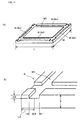
- Part (a) of Fig. 1 is a cross-sectional view schematically showing an infrared sensor according to an embodiment (a first embodiment) of the present invention.
- Part (b) of Fig. 1 is a perspective view of the same.
- Part (a) of Fig. 2 is a perspective view showing a configuration of an optical filter used for the infrared sensor of the first embodiment.
- Part (b) of Fig. 2 is an enlarged view of a primary portion of the same.
- This infrared sensor includes an infrared sensor element 1, a package 2, and an optical filter 3.
- the package 2 in which the infrared sensor element is accommodated is made of metal for surface mounting, and has a box-like shape with an opening 2a formed at a surface (an upper surface shown in part (b) of Fig. 1 ) so as to have an inner space (a sealed space) 2b in which the infrared sensor element 1 is accommodated.
- the package 2 also has a wiring pattern 11 therein.
- the optical filter 3 covers the entire area of the opening 2a of the package 2.
- the optical filter 3 provides a function of allowing the infrared sensor element 1 to receive infrared radiation with a predetermined wavelength, and also, a function as a cover to seal the opening 2a of the package 2.
- the infrared sensor element 1 is a so-called dual type infrared sensor element having a pyroelectric element 1a polarized in a thickness direction, and two electrodes (light-receiving electrodes) 10a and 10b disposed on a surface of the pyroelectric element 1a.
- the electrodes 10a and 10b are connected in series to have reversed polarities, so that external noises (e.g., temperature variation of surrounding environment) concurrently input to the two light-receiving electrodes 10a and 10b are canceled with each other.
- the package 2 has a box-like shape and is made of metal (for example, 42-Ni, phosphor bronze, brass, nickel silver, or iron) with a substantially entire area of an upper surface thereof being open. A part of the inner side and a part of the outer side of the package 2 are lined with an insulating material 4, such as glass or LCP resin (liquid crystal polymer). A wiring pattern 11, which is required for the configuration of the infrared sensor, is provided on the surface of the insulating material 4.
- metal for example, 42-Ni, phosphor bronze, brass, nickel silver, or iron
- the opening 2a of the package 2 has a rectangular profile in plan view.
- Supporting portions (bases) 12 are disposed on the bottom surface of the package 2, for supporting the infrared sensor element 1.
- the infrared sensor element 1 is supported on the supporting portions (bases) 12.
- outer connection terminals (outer electrodes) 5 are provided at predetermined positions of the package 2 made of metal.
- the outer connection terminals 5 are insulated by an insulator (glass in the first embodiment) so as not to conduct to the package 2.
- the infrared sensor element 1 disposed in the package 2 is electrically connected to external devices through the wiring pattern provided in the package 2 and the outer connection terminals (outer electrodes) 5.
- the optical filter 3 employs an optical filter having a resistance of 1 M ⁇ /cm or less and made of monocrystal silicon which transmits infrared radiation with a predetermined wavelength.
- the optical filter 3 has a rectangular shape in plan view substantially corresponding to the shape of the opening 2a formed at the upper surface of the package 2.
- the optical filter 3 employed in the first embodiment measures 8.8 mm in length (L), 6.8 mm in width (W), and 0.5 mm in thickness (T).
- grooves 8 (8a, 8b, 8c, 8d) are formed at a peripheral portion of the optical filter 3 in a region opposed to a circumferential region of the opening 2a of the package 2.
- the grooves 8 extend in parallel to the edges of the optical filter 3.
- An annular groove 80 continuously located in the peripheral portion of the optical filter 3 is defined by portions (inner portions) of the grooves 8, excluding outer portions (near the edges) of the grooves 8 with respect to the intersections of the grooves 8.
- the grooves 8 are formed by half-cutting the optical filter 3 using a dicing blade with a thickness of 0.30 mm.
- Each groove 8 (80) measures 0.1 mm in depth (D1) and 0.30 mm in width (W1, width of the blade).
- a distance (L1) from an edge of the optical filter 3 to the center in a width direction of the groove 8 (80) is 0.24 mm.
- the region of the optical filter 3 including the annular groove 80 at the surface opposed to the opening 2a of the package 2 is mechanically joined to the circumferential region of the opening 2a of the package 2 by a conductive adhesive 7. Accordingly, the opening 2a of the package 2 is reliably sealed with the optical filter 3, and the optical filter 3 is electrically connected to the package 2 reliably via the conductive adhesive 7.
- the annular groove 80 is formed at the peripheral portion of the optical filter 3 in the region opposed to the circumferential region of the opening 2a of the package 2 to be continuously located in the peripheral portion of the optical filter 3, and the peripheral portion of the optical filter 3 is joined to the circumferential region of the opening 2a of the package 2 by the conductive adhesive 7 held in the annular groove 80 continuously located in the peripheral portion of the optical filter 3. Accordingly, the optical filter 3 is reliably connected to the package 2 mechanically and electrically.
- the infrared sensor element 1 Since a reliability of joining the optical filter 3 to the package 2 is enhanced without requiring a complicated structure or a complicated manufacturing procedure, and the infrared sensor element 1 is accommodated in the sealed space 2b defined by the electrically connected optical filter 3 and package 2, the infrared sensor having a high electromagnetic-shielding performance and a reliable electromagnetic-wave-proof characteristic can be provided.
- the annular groove 80 continuously located in the peripheral portion of the optical filter 3 holds the conductive adhesive 7, the conductive adhesive 7 can be prevented from flowing to a central region from the peripheral portion of the optical filter 3, thereby providing a sufficient field of view and a high detection reliability.
- the optical filter body of the optical filter 3 is made of a low-resistance material.
- the optical filter 3 can be reliably joined to the package 2 without requiring a complicated manufacturing procedure, and also the conductive adhesive 7 can be restricted and prevented from flowing to the central region from the peripheral portion of the optical filter 3, thereby providing the sufficient field of view (namely, infrared radiation with a predetermined wavelength can be reliably transmitted through the central region). Therefore, the infrared sensor with a high reliability can be provided, which is the principal advantage of the present invention.
- the present invention may be applied to various optical filters regardless of the configuration of the optical filter.
- the present invention may be applied to any of the following cases:
- the package 2 since the package 2 has the wiring pattern 11, wiring patterns required to be formed at other members may be reduced, thereby reducing the size of a product and reducing the number of components.
- the optical filter 3 can be joined to the package 2 without other components interposed therebetween, the size of the product can be reduced and the manufacturing procedure can be simplified, thereby reducing the cost.
- the package 2 has the supporting portions (bases) 12 for supporting the infrared sensor element 1, additional supporting members are not required, and thus, the number of components can be reduced and the size of the product can be reduced.
- the size of the product can be further reduced.
- Part (a) of Fig. 4 is a cross-sectional view schematically showing an infrared sensor according to another embodiment (a second embodiment) of the present invention.
- Part (b) of Fig. 4 is a perspective view of the same.
- Part (a) of Fig. 5 is a perspective view showing a configuration of an optical filter used for the infrared sensor of the second embodiment.
- Part (b) of Fig. 5 is an enlarged view of a primary portion of the same.
- the infrared sensor of the second embodiment has the following configurations.
- W2 represents the width of the groove formed at the optical filter 3
- L2 represents a distance from the edge of the optical filter 3 to the center in the width direction of the groove 8 (80).
- the annular groove 80 is formed at the peripheral portion of the optical filter 3, at the surface provided with the thin film 34 made of the insulating material in the region opposed to the circumferential region of the opening 2a of the package 2 to be continuously located in the peripheral portion of the optical filter 3.
- the peripheral portion of the optical filter 3 can be reliably joined to the circumferential region of the opening 2a of the package 2 by the conductive adhesive 7 held in the annular groove 80 formed at the optical filter 3, in a manner similar to the infrared sensor of the above-described first embodiment.
- the optical filter 3 has the thin film 34 made of the insulating material at the surface of the optical filter 3.
- the annular groove 80 is formed to extend from the surface provided with the thin film 34 made of the insulating material to the filter body 33, the optical filter 3 can be electrically reliably connected to the package 2 by the conductive adhesive 7 held in the annular groove 80.
- the infrared sensor element 1 is accommodated in the sealed space 2b defined by the optical filter 3 and the package 2 which are electrically connected to each other, thereby providing an infrared sensor having a high electromagnetic-shielding performance.
- the conductive adhesive 7 since the conductive adhesive 7 is held at the annular groove 80 formed to be continuously located in the peripheral portion of the optical filter 3, the conductive adhesive 7 can be prevented from flowing to the central region from the peripheral portion of the optical filter 3, thereby providing a sufficient field of view and a high detection reliability.
- the package 2 has the wiring pattern 11, wiring patterns required to be provided at other members may be reduced, thereby reducing the size of the product and the number of components. Also, since the optical filter 3 can be joined to the package 2 without other components interposed therebetween, the size of the product can be reduced and the manufacturing procedure can be simplified, thereby reducing the cost. Further, since the package 2 has the supporting portions (bases) 12 for supporting the infrared sensor element 1, additional supporting members are not required, and thus, the number of components can be reduced and the size of the product can be reduced.
- the infrared sensor element is the dual type using the pyroelectric elements
- the infrared sensor element of the present invention is not limited to that type, and may be single type or quad type, or the present invention may be applied to an infrared sensor using various types of infrared sensor elements such as a thermopile and a photodiode.
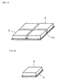
- Figs. 7 to 9 are illustrations showing a method of manufacturing the infrared sensor according to still another embodiment (a third embodiment) of the present invention (in the third embodiment, the method corresponding to the manufacturing method of the infrared sensor described in the first embodiment).
- the method of manufacturing the infrared sensor according to the third embodiment relates to a method of manufacturing an infrared sensor in which a plurality of packages that accommodate infrared sensor elements are disposed on a mother optical filter, and the plurality of packages are bonded and fixed thereto and then divided into individual infrared sensors, thereby manufacturing a plurality of infrared sensors at a time.
- grooves 80a which become grooves 80 continuously located in peripheral portions of optical filters 3 after being divided are formed at a mother optical filter 43 which contains the optical filters 3 corresponding to the plurality of infrared sensors.
- the conductive adhesive 7 is applied to the grooves 80a which become the grooves 80 continuously located in the peripheral portions of the optical filters 3 and to the vicinities of the grooves 80a.
- the plurality of packages 2 that accommodate the infrared sensor elements are placed on the mother optical filter 43 such that the circumferential regions of the openings of the packages 2 come into contact with the conductive adhesive 7 applied at the grooves 80a and the vicinities thereof.
- the plurality of packages 2 are bonded and fixed to the mother optical filter 43 by curing the conductive adhesive 7.
- the mother optical filter 43 is divided at predetermined positions to obtain the individual infrared sensors ( Fig. 9 ).
- the plurality of infrared sensors can be manufactured efficiently at a time.
- Part (a) of Fig. 10 is a cross-sectional view schematically showing an infrared sensor according to yet another embodiment (a fourth embodiment) of the present invention.
- Part (b) of Fig. 10 is a perspective view of the same.
- Part (a) of Fig. 11 is a perspective view showing a configuration of an optical filter used for the infrared sensor of the fourth embodiment.
- Part (b) of Fig. 11 is an enlarged view of a primary portion of the same.
- Fig. 12 is an illustration showing a state where the circumferential region of the opening of the package is fitted to the grove continuously located in the peripheral portion of the optical filter.
- the circumferential region (an end portion) 22 of the opening 2a of the package 2 is fitted to the annular groove 80 defined by the grooves 8a, 8b, 8c to be continuously located in the peripheral portion of the optical filter 3, and 8d.
- the end portion 22 of the package 2 is fixed to the groove 80 of the optical filter 3 by the conductive adhesive 7.
- the annular groove 80 is formed to be larger than the circumferential region (the end portion) 22 of the package 2 such that the width of the groove 80 is larger than the width of the circumferential region (the end portion) 22 of the package 2.
- the circumferential region (the end portion) 22 is fitted to the groove 80 of the optical filter 3.
- Each groove 8 (80) measures 0.1 mm in depth (D3) and 0.04 mm in width (W3, width of the blade).
- a distance (L3) from the edge of the optical filter 3 to the center in the width direction of the groove 8 (80) is 0.24 mm.
- the infrared sensor of the fourth embodiment has the configuration in which the circumferential region (the end portion) 22 of the opening 2a of the package 2 is fitted to the groove 80 continuously located in the peripheral portion of the optical filter 2, when the optical filter 3 is mounted on the package 2, the positional accuracy can be enhanced, and the positional shift of the optical filter 3 can be prevented after mounting, thereby providing a highly reliable infrared sensor.
- the optical filter having the two-layer structure that is composed of the filter body and the thin film made of the insulating material may be employed as the optical filter 2.
- Figs. 13 to 15 are illustrations showing a method of manufacturing the infrared sensor according to still another embodiment (a fifth embodiment) of the present invention (in the fifth embodiment, the method corresponding to the manufacturing method of the infrared sensor described in the fourth embodiment).
- the method of manufacturing the infrared sensor according to the fifth embodiment relates to a method of manufacturing an infrared sensor in which a plurality of packages that accommodate infrared sensor elements are disposed on a mother optical filter, and the plurality of packages are bonded and fixed thereto and then divided into individual infrared sensors, thereby manufacturing a plurality of infrared sensors at a time.
- grooves 80a which become grooves 80 continuously located in peripheral portions of optical filters 3 after being divided are formed at the mother optical filter 43 including the optical filters 3 corresponding to the plurality of infrared sensors.
- the grooves 80a are formed to have a width that allows the circumferential regions (the end portions) 22 of the openings 2a of the packages 2 to be fitted to the grooves 80a.
- the conductive adhesive 7 is applied to the grooves 80a which become the grooves 80 continuously located in the peripheral portions of the optical filters 3.
- the plurality of packages 2 that accommodate the infrared sensor elements are placed on the mother optical filter 43 such that the circumferential regions of the openings of the packages 2 are fitted to the grooves 80a and come into contact with the conductive adhesive 7 applied at the grooves 80a.
- the plurality of packages 2 are bonded and fixed to the mother optical filter 43 by curing the conductive adhesive 7.
- the mother optical filter 43 is divided at predetermined positions to obtain the individual infrared sensors ( Fig. 15 ).
- the plurality of infrared sensors can be manufactured efficiently at a time.
- the packages 2 are placed on the mother optical filter 43 such that the circumferential regions (the end portions) 22 of the openings 2a of the packages 2 are fitted to the grooves 80a that become the grooves continuously located in the peripheral portions of the optical filters. Therefore, the positional shift may be reduced.
- the adhesive can be applied before the packages 2 are mounted, but also the adhesive can be applied after the packages 2 are mounted and then the packages 2 are bonded and fixed to the mother optical filter 43. This may allow the manufacturing procedure to be designed freely, and to be rationalized.
- the optical filter is made of monocrystal silicon in the first to fifth embodiments, it is not limited to the monocrystal silicon.
- the optical filter body may be made of various materials that transmit infrared radiation, such as quartz, sapphire, barium fluoride, and spinel.
- the filter body is made of an insulator such as quartz
- a metal film is deposited on the surface of the body so as to be conductive.
- the adhesive may be prevented from flowing to an unwanted region of the optical filter and reducing the field of view, and also the optical filter may be reliably joined to the package, without requiring a complicated structure or a complicated manufacturing procedure.
- the configuration may be easily and reliably provided that the infrared sensor element is accommodated in the sealed space defined by the optical filter and the package electrically connected to each other, thereby having a high electromagnetic-shielding performance.
- the present invention may be applied to general purpose infrared sensors used for human detection, security apparatuses, and the like.
Landscapes
- Physics & Mathematics (AREA)
- General Physics & Mathematics (AREA)
- Spectroscopy & Molecular Physics (AREA)
- Photometry And Measurement Of Optical Pulse Characteristics (AREA)
Abstract
Description
- The present invention relates to an infrared sensor and its manufacturing method, the infrared sensor having a configuration in which an infrared sensor element is accommodated in a package. More particularly, the present invention relates to an infrared sensor and its manufacturing method, the infrared sensor having a configuration in which an infrared sensor element is accommodated in a sealed space defined by a package and an optical filter which also serves as a cover.
- As shown in parts (a) and (b) of
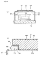
Fig. 16 , a known infrared sensor is disclosed (see Patent Document 1). The infrared sensor has a configuration in which aninfrared sensor element 54 is accommodated in a sealedspace 53 defined by acontainer body 51 and astem 52, and a filter (window member) 57 is disposed at an upper surface of thecontainer body 51. The filter (window member) 57 has asubstrate 55 andinfrared filter layers substrate 55 so as to transmit infrared radiation with a predetermined wavelength. - In such an infrared sensor, as shown in part (b) of
Fig. 16 , astep 57a is provided at a peripheral portion of a lower surface of thefilter 57. Thestep 57a is engaged with anopening 58 formed at the upper surface of thecontainer body 51, and then, a metalthin film 59 which is provided on a surface of thestep 57a of thefilter 57 by sputtering is joined to the opening 58 of thecontainer body 51 by using asolder 60, so that thefilter 57 is attached to the opening 58 of thecontainer body 51. - However, with the method described in
Patent Document 1, as shown in part (b) ofFig. 16 , the metalthin film 59 is required to be provided on the surface of thestep 57a by sputtering or the like after thestep 57a is formed at the peripheral portion of thefilter 57. This may cause the manufacturing procedure to be complicated, resulting in an increase in cost. - In addition, when the metal
thin film 59 provided on thestep 57a of thefilter 57 is joined to the opening 58 of thecontainer body 51 by using thesolder 60, it is difficult to distribute thesolder 60 so as to be continuously located in the peripheral portion of the opening 58 of thecontainer body 51 for reliably joining thefilter 57 to thecontainer body 51. If thesolder 60 is distributed unevenly at a gap between thestep 57a and theopening 58 of thecontainer body 51, thesolder 60 may flow to theinfrared filter layer 56b provided at the lower surface of the filter 57 (namely, to a center region of theinfrared filter layer 56a), thereby degrading its reliability, such as that a field of view is narrowed. - As shown in
Fig. 17 , another infrared sensor is suggested (see Patent Document 2). The infrared sensor has a configuration in which astep 63 is formed to be continuously located in a circumferential portion of an opening 62 of aceramic package 61, and acover 65 is fitted to thestep 63. Thecover 65 has aninfrared sensor element 64 attached to a lower surface, and an infrared-insulating film 68 attached to an upper surface in a region not occupied by awindow 67 so that only a portion (the window) 67 can transmit the infrared radiation. Afiller 66 such as epoxy resin is injected to a gap between thecover 65 and the opening 62 of theceramic package 61, and then thecover 65 is attached to theceramic package 61. - However, with the method of
Patent Document 2, thefiller 66 is not applied sufficiently to the gap between opposed surfaces of thecover 65 andceramic package 61, resulting in unstable sealing. - If the
filler 66 is sufficiently applied to the gap between the opposed surfaces of thecover 65 andceramic package 61, thefiller 66 may flow to a central region at the lower surface of thecover 65. - Patent Document 1:
Japanese Unexamined Patent Application Publication No. 6-201454 - Patent Document 2:
Japanese Unexamined Patent Application Publication No. 10-318829 - The present invention is made for solving the above-mentioned problems. Accordingly, an object of the present invention is to provide a highly reliable infrared sensor and its manufacturing method, the infrared sensor having a configuration capable of enhancing a reliability of joining an optical filter to a package without requiring a complicated structure or a complicated manufacturing procedure, and without causing a problem that an adhesive flows to a region interfering with the field of view of the optical filter. Further, another object of the present invention is to provide an infrared sensor and its manufacturing method, the infrared sensor having an excellent electromagnetic-shielding performance and a reliable electromagnetic-wave-proof characteristic.
- To solve the above-mentioned problems, an infrared sensor according to
claim 1 includes an infrared sensor element; a package for surface mounting and having a box-like shape with an opening formed at a surface, the package being configured to accommodate the infrared sensor element therein; and an optical filter configured to transmit infrared radiation with a predetermined wavelength, the optical filter being arranged to cover the opening of the package, a peripheral portion of the optical filter being joined to a circumferential region of the opening of the package by an adhesive, the optical filter providing a function of allowing the infrared sensor element to receive the infrared radiation with the predetermined wavelength and a function as a cover to seal the opening. A groove is formed at the peripheral portion of the optical filter in a region opposed to the circumferential region of the opening of the package so as to surround the optical filter. - Based on the invention described in
claim 1, in an infrared sensor according toclaim 2, the optical filter has a resistance of 1 MΩ/cm or less, the package is mainly composed of a metal material, and the adhesive for joining the optical filter to the package is a conductive adhesive, and the optical filter is electrically connected to the package with the conductive adhesive interposed therebetween. - Based on the invention described in
claim claim 3, the optical filter has a filter body and a thin film, the filter body providing the function of allowing the infrared sensor element to receive the infrared radiation with the predetermined wavelength and the function as the cover to seal the opening, the thin film being made of an insulating material and provided on a surface of the filter body. The groove continuously located in the peripheral portion of the optical filter extends from the surface provided with the thin film made of the insulating material to the filter body. - Based on the invention described in any one of
claims 1 to 3, in an infrared sensor according toclaim 4, the circumferential region of the opening of the package is fitted to the groove continuously located in the peripheral portion of the optical filter. - A method of manufacturing an infrared sensor according to
claim 5 is a method of manufacturing the infrared sensor described in any one ofclaims 1 to 3. The method includes the steps of forming a plurality of grooves at a mother optical filter that contains a plurality of the optical filters corresponding to a plurality of the infrared sensors, the grooves becoming a plurality of the grooves continuously located in a plurality of the peripheral portions of the optical filters after being divided; applying the adhesive at the grooves and the vicinities thereof; placing a plurality of the packages that accommodate a plurality of the infrared sensor elements on the mother optical filter such that a plurality of the circumferential regions of a plurality of the openings come into contact with the adhesive applied at the grooves and the vicinities thereof, and bonding and fixing the packages to the mother optical filter by the adhesive; and dividing the mother optical filter at predetermined positions so as to obtain the individual infrared sensors. - A method of manufacturing an infrared sensor according to
claim 6 is a method of manufacturing the infrared sensor described inclaim 4. The method includes the steps of forming a plurality of grooves at a mother optical filter that contains a plurality of the optical filters corresponding to a plurality of the infrared sensors, the grooves becoming a plurality of the grooves continuously located in a plurality of the peripheral portions of the optical filters after being divided; placing a plurality of the packages that accommodate a plurality of the infrared sensor elements on the mother optical filter such that a plurality of the circumferential regions of a plurality of the openings are fitted to the grooves that become the grooves continuously located in the peripheral portions of the optical filters, and in this state, bonding and fixing the packages to the mother optical filter by the adhesive; and dividing the mother optical filter at predetermined positions so as to obtain the individual infrared sensors. Advantages - The infrared sensor according to
claim 1 includes the infrared sensor element, the package for surface mounting and having the box-like shape with the opening formed at the surface, the package being configured to accommodate the infrared sensor element therein, and the optical filter configured to transmit the infrared radiation with the predetermined wavelength, the optical filter being arranged to cover the opening of the package, the peripheral portion of the optical filter being joined to the circumferential region of the opening of the package by the adhesive, the optical filter providing the function of allowing the infrared sensor element to receive the infrared radiation with the predetermined wavelength and the function as the cover to seal the opening. The groove is formed at the peripheral portion of the optical filter in the region opposed to the circumferential region of the opening of the package so as to be continuously located in the peripheral portion of the optical filter. Accordingly, the peripheral portion of the optical filter is reliably joined to the circumferential region of the opening of the package by the adhesive held at the groove. - Since the groove formed to be continuously located in the peripheral portion of the optical filter holds the adhesive, the adhesive may be reliably inhibited and prevented from flowing to the central region from the peripheral portion of the optical filter.
- Therefore, the adhesive may be prevented from flowing to an unwanted region of the optical filter and from narrowing the field of view, while the optical filter may be reliably joined to the package, without requiring a complicated structure or a complicated manufacturing procedure, thereby providing an infrared sensor which is economically efficient and highly reliable.
- Based on the invention described in
claim 1, in the infrared sensor according toclaim 2, the optical filter has the resistance of 1 MΩ/cm or less, the package is mainly composed of the metal material, and the adhesive for joining the optical filter to the package is the conductive adhesive, and the optical filter is electrically connected to the package with the conductive adhesive interposed therebetween. In this case, the infrared sensor element is accommodated in the sealed space defined by the optical filter and the package electrically connected to each other, thereby providing an infrared sensor with an excellent electromagnetic-shielding performance and a reliable electromagnetic-wave-proof characteristic. - Based on the invention described in
claim claim 3, the optical filter has the filter body and the thin film, the filter body providing the function of allowing the infrared sensor element to receive the infrared radiation with the predetermined wavelength and the function as the cover to seal the opening, the thin film being made of the insulating material and provided on the surface of the filter body. Also, the groove continuously located in the peripheral portion of the optical filter extends from the surface provided with the thin film made of the insulating material to the filter body. In this case, the peripheral portion of the optical filter is reliably joined to the circumferential region of the opening of the package by the adhesive held at the groove. - Therefore, in the case where the optical filter has the filter body and the thin film made of the insulating material provided on the surface of the filter body, the adhesive may be prevented from flowing to an unwanted region of the optical filter and from narrowing the field of view, while the optical filter may be reliably joined to the package, without requiring a complicated structure or a complicated manufacturing procedure, thereby providing an infrared sensor which is economically efficient and highly reliable.
- In addition, since the conductive adhesive is sufficiently held at the groove having the depth extending from the surface provided with the thin film made of the insulating material to the filter body, the optical filter may be electrically connected to the package with the conductive adhesive interposed therebetween. Accordingly, the infrared sensor element may be accommodated in the sealed space defined by the optical filter and the package electrically connected to each other, thereby providing a highly reliable infrared sensor having an excellent electromagnetic-shielding performance.
- For example, the filter body that may be applied to the present invention may be made of various materials, such as monocrystal silicon, quartz, sapphire, barium fluoride, and spinel. In the present invention, however, the filter body may employ other material.
- In the present invention, the insulating material for the thin film may be ZnS, Ge, or the like.
- Based on the invention described in any one of
claims 1 to 3, in the infrared sensor according toclaim 4, the circumferential region of the opening of the package is fitted to the groove continuously located in the peripheral portion of the optical filter. Accordingly, the positional accuracy may be enhanced when the optical filter is mounted on the package, moreover the positional shift after mounting may be prevented, thereby enhancing the reliability. - The method of manufacturing an infrared sensor according to
claim 5 is the method of manufacturing the infrared sensor described in any one ofclaims 1 to 3. The method includes forming the grooves at the mother optical filter that contains the optical filters corresponding to the infrared sensors, the grooves becoming the grooves continuously located in the peripheral portions of the optical filters after being divided, applying the adhesive at the grooves and the vicinities thereof, placing the packages that accommodate the infrared sensor elements on the mother optical filter such that the circumferential regions of the openings come into contact with the adhesive applied at the grooves and the vicinities thereof, and bonding and fixing the packages to the mother optical filter by the adhesive and dividing the mother optical filter at the predetermined positions so as to obtain the individual infrared sensors. In the manufacturing procedure, the mother optical filter serves as a tray or as a substrate for conveying the packages. Accordingly, the plurality of infrared sensors can be manufactured efficiently at a time by dividing the mother optical filter after the bonding and fixing of the packages. - The method of manufacturing the infrared sensor according to
claim 6 is the method of manufacturing the infrared sensor described inclaim 4. The method includes forming the grooves at the mother optical filter that contains the optical filters corresponding to the infrared sensors, the grooves becoming the grooves continuously located in the peripheral portions of the optical filters after being divided, placing the packages that accommodate the infrared sensor elements on the mother optical filter such that the circumferential regions of the openings are fitted to the grooves that become the grooves continuously located in the peripheral portions of the optical filters, and in this state, bonding and fixing the packages to the mother optical filter by the adhesive, and dividing the mother optical filter at the predetermined positions so as to obtain the individual infrared sensors. In the manufacturing procedure, the mother optical filter serves as a tray or as a substrate for conveying the packages. Accordingly, the plurality of infrared sensors can be manufactured efficiently at a time by dividing the mother optical filter after the bonding and fixing of the packages. - In addition, since the plurality of packages are mounted on the mother optical filter such that the circumferential regions of the openings of the packages are fitted to the grooves formed at the mother optical filter, the grooves becoming grooves continuously located in the peripheral portion of the optical filter, the positional shift may be reduced in the subsequent procedure. Accordingly, the plurality of infrared sensors can be further reliably manufactured efficiently at a time.
- In the case of the method of manufacturing the infrared sensor according to
claim 6, the packages are placed on the mother optical filter such that the circumferential regions of the openings of the packages are fitted to the grooves that become the grooves continuously located in the peripheral portions of the optical filters. Therefore, the positional shift may be reduced. Thus, not only the adhesive can be applied before the packages are mounted, but also the adhesive can be applied after the packages are mounted and then the packages are bonded and fixed to the mother optical filter. This may allow the manufacturing procedure to be designed freely, and to be rationalized, thereby reducing the cost. -
- Part (a) of
Fig. 1 is a cross-sectional view schematically showing an infrared sensor according to an embodiment (a first embodiment) of the present invention. Part (b) ofFig. 1 is a perspective view of the same. - Part (a) of
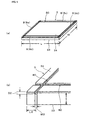
Fig. 2 is a perspective view showing a configuration of an optical filter used for the infrared sensor of the first embodiment. Part (b) ofFig. 2 is an enlarged view of a primary portion of the same. -
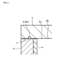
Fig. 3 is an illustration showing an essential structure of the infrared sensor according to the embodiment (the first embodiment) of the present invention. - Part (a) of
Fig. 4 is a cross-sectional view schematically showing an infrared sensor according to another embodiment (a second embodiment) of the present invention. Part (b) ofFig. 4 is a perspective view of the same. - Part (a) of
Fig. 5 is a perspective view showing a configuration of an optical filter used for the infrared sensor of the second embodiment. Part (b) ofFig. 5 is an enlarged view of a primary portion of the same. -
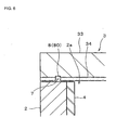
Fig. 6 is an illustration showing an essential structure of the infrared sensor according to the second embodiment of the present invention. -
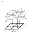
Fig. 7 is an illustration showing a procedure of manufacturing an infrared sensor according to a third embodiment of the present invention. -
Fig. 8 is an illustration showing another procedure of manufacturing the infrared sensor according to the third embodiment of the present invention. -
Fig. 9 is an illustration showing still another procedure of manufacturing the infrared sensor according to the third embodiment of the present invention. - Part (a) of
Fig. 10 is a cross-sectional view schematically showing an infrared sensor according to an embodiment (a fourth embodiment) of the present invention. Part (b) ofFig. 10 is a perspective view of the same. - Part (a) of
Fig. 11 is a perspective view showing a configuration of an optical filter used for the infrared sensor of the fourth embodiment. Part (b) ofFig. 11 is an enlarged view of a primary portion of the same. -
Fig. 12 is an illustration showing an essential structure of the infrared sensor according to the embodiment (the fourth embodiment) of the present invention. -
Fig. 13 is an illustration showing a procedure of manufacturing an infrared sensor according to a fifth embodiment of the present invention. -
Fig. 14 is an illustration showing another procedure of manufacturing the infrared sensor according to the fifth embodiment of the present invention. -
Fig. 15 is an illustration showing still another procedure of manufacturing the infrared sensor according to the fifth embodiment of the present invention. - Parts (a) and (b) of
Fig. 16 are illustrations each showing a configuration of a known infrared sensor. -
Fig. 17 is an illustration showing a configuration of another known infrared sensor. -
- 1
- infrared sensor element
- 1a
- pyroelectric element
- 2
- package
- 2a
- opening of package
- 2b
- inner space (sealed space)
- 3
- optical filter
- 4
- insulating material
- 5
- outer connection terminal (outer electrode)
- 6
- insulator (glass)
- 7
- conductive adhesive
- 8 (8a, 8b, 8c, 8d)
- groove
- 10a, 10b
- electrode (light-receiving electrode)
- 11
- wiring pattern
- 12
- supporting portion (base)
- 13
- by-pass capacitor
- 14
- FET
- 15
- resistance
- 22
- circumferential region (end portion) of opening
- 33
- filter body
- 34
- thin film made of insulating material
- 43
- mother optical filter
- 80
- annular groove
- 80a
- groove
- D1, D2, D3
- depth of groove
- L
- length of optical filter
- L1, L2, L3
- distance from edge of optical filter to center in width direction of groove
- T
- thickness of optical filter
- W
- width of optical filter
- W1, W2, W3
- width of groove
- Features of the present invention are described below in detail with reference to embodiments of the present invention.
- Part (a) of
Fig. 1 is a cross-sectional view schematically showing an infrared sensor according to an embodiment (a first embodiment) of the present invention. Part (b) ofFig. 1 is a perspective view of the same. Part (a) ofFig. 2 is a perspective view showing a configuration of an optical filter used for the infrared sensor of the first embodiment. Part (b) ofFig. 2 is an enlarged view of a primary portion of the same. - This infrared sensor includes an
infrared sensor element 1, apackage 2, and anoptical filter 3. Thepackage 2 in which the infrared sensor element is accommodated is made of metal for surface mounting, and has a box-like shape with anopening 2a formed at a surface (an upper surface shown in part (b) ofFig. 1 ) so as to have an inner space (a sealed space) 2b in which theinfrared sensor element 1 is accommodated. Thepackage 2 also has awiring pattern 11 therein. Theoptical filter 3 covers the entire area of theopening 2a of thepackage 2. Theoptical filter 3 provides a function of allowing theinfrared sensor element 1 to receive infrared radiation with a predetermined wavelength, and also, a function as a cover to seal theopening 2a of thepackage 2. - The
infrared sensor element 1 is a so-called dual type infrared sensor element having a pyroelectric element 1a polarized in a thickness direction, and two electrodes (light-receiving electrodes) 10a and 10b disposed on a surface of the pyroelectric element 1a. Theelectrodes electrodes - The
package 2 has a box-like shape and is made of metal (for example, 42-Ni, phosphor bronze, brass, nickel silver, or iron) with a substantially entire area of an upper surface thereof being open. A part of the inner side and a part of the outer side of thepackage 2 are lined with an insulatingmaterial 4, such as glass or LCP resin (liquid crystal polymer). Awiring pattern 11, which is required for the configuration of the infrared sensor, is provided on the surface of the insulatingmaterial 4. - The
opening 2a of thepackage 2 has a rectangular profile in plan view. Supporting portions (bases) 12 are disposed on the bottom surface of thepackage 2, for supporting theinfrared sensor element 1. Theinfrared sensor element 1 is supported on the supporting portions (bases) 12. - A by-
pass capacitor 13, anFET 14, and aresistance 15, which are required for the configuration of the infrared sensor, are disposed in thepackage 2 so as to conduct to electrodes and wiring (not shown). - In the infrared sensor of the first embodiment, outer connection terminals (outer electrodes) 5 are provided at predetermined positions of the
package 2 made of metal. Theouter connection terminals 5 are insulated by an insulator (glass in the first embodiment) so as not to conduct to thepackage 2. Thus, theinfrared sensor element 1 disposed in thepackage 2 is electrically connected to external devices through the wiring pattern provided in thepackage 2 and the outer connection terminals (outer electrodes) 5. - The
optical filter 3 employs an optical filter having a resistance of 1 MΩ/cm or less and made of monocrystal silicon which transmits infrared radiation with a predetermined wavelength. Theoptical filter 3 has a rectangular shape in plan view substantially corresponding to the shape of theopening 2a formed at the upper surface of thepackage 2. Theoptical filter 3 employed in the first embodiment measures 8.8 mm in length (L), 6.8 mm in width (W), and 0.5 mm in thickness (T). - As shown in parts (a) and (b) of
Fig. 2 , grooves 8 (8a, 8b, 8c, 8d) are formed at a peripheral portion of theoptical filter 3 in a region opposed to a circumferential region of theopening 2a of thepackage 2. Thegrooves 8 extend in parallel to the edges of theoptical filter 3. Anannular groove 80 continuously located in the peripheral portion of theoptical filter 3 is defined by portions (inner portions) of thegrooves 8, excluding outer portions (near the edges) of thegrooves 8 with respect to the intersections of thegrooves 8. - In this embodiment, the
grooves 8 are formed by half-cutting theoptical filter 3 using a dicing blade with a thickness of 0.30 mm. - Each groove 8 (80) measures 0.1 mm in depth (D1) and 0.30 mm in width (W1, width of the blade). A distance (L1) from an edge of the
optical filter 3 to the center in a width direction of the groove 8 (80) is 0.24 mm. - As shown in
Fig. 3 , the region of theoptical filter 3 including theannular groove 80 at the surface opposed to theopening 2a of thepackage 2 is mechanically joined to the circumferential region of theopening 2a of thepackage 2 by aconductive adhesive 7. Accordingly, theopening 2a of thepackage 2 is reliably sealed with theoptical filter 3, and theoptical filter 3 is electrically connected to thepackage 2 reliably via theconductive adhesive 7. - In the infrared sensor with the above-described configuration, the
annular groove 80 is formed at the peripheral portion of theoptical filter 3 in the region opposed to the circumferential region of theopening 2a of thepackage 2 to be continuously located in the peripheral portion of theoptical filter 3, and the peripheral portion of theoptical filter 3 is joined to the circumferential region of theopening 2a of thepackage 2 by theconductive adhesive 7 held in theannular groove 80 continuously located in the peripheral portion of theoptical filter 3. Accordingly, theoptical filter 3 is reliably connected to thepackage 2 mechanically and electrically. - Since a reliability of joining the
optical filter 3 to thepackage 2 is enhanced without requiring a complicated structure or a complicated manufacturing procedure, and theinfrared sensor element 1 is accommodated in the sealedspace 2b defined by the electrically connectedoptical filter 3 andpackage 2, the infrared sensor having a high electromagnetic-shielding performance and a reliable electromagnetic-wave-proof characteristic can be provided. - Also, in the infrared sensor of the first embodiment, since the
annular groove 80 continuously located in the peripheral portion of theoptical filter 3 holds theconductive adhesive 7, theconductive adhesive 7 can be prevented from flowing to a central region from the peripheral portion of theoptical filter 3, thereby providing a sufficient field of view and a high detection reliability. - In the first embodiment, the optical filter body of the
optical filter 3 is made of a low-resistance material. However, even when the optical filter body is made of an insulating material, theoptical filter 3 can be reliably joined to thepackage 2 without requiring a complicated manufacturing procedure, and also theconductive adhesive 7 can be restricted and prevented from flowing to the central region from the peripheral portion of theoptical filter 3, thereby providing the sufficient field of view (namely, infrared radiation with a predetermined wavelength can be reliably transmitted through the central region). Therefore, the infrared sensor with a high reliability can be provided, which is the principal advantage of the present invention. - The present invention may be applied to various optical filters regardless of the configuration of the optical filter. For example, the present invention may be applied to any of the following cases:
- (1) a case where an optical filter is made of a low-resistance material (the case of the first embodiment),
- (2) a case where an optical filter is formed such that a low-resistance material (layer) is arranged on the surface of a filter body (layer) made of an insulating material,
- (3) a case where an optical filter is formed such that a low-resistance material (layer) is arranged on the surface of a filter body (layer) made of a low-resistance material, and
- (4) a case where an optical filter is formed such that an insulating material (layer) is arranged on the surface of a filter body (layer) made of a low-resistance material (the case of a second embodiment described below).
- In the infrared sensor of the first embodiment, since the
package 2 has thewiring pattern 11, wiring patterns required to be formed at other members may be reduced, thereby reducing the size of a product and reducing the number of components. - Since the
optical filter 3 can be joined to thepackage 2 without other components interposed therebetween, the size of the product can be reduced and the manufacturing procedure can be simplified, thereby reducing the cost. - Since the
package 2 has the supporting portions (bases) 12 for supporting theinfrared sensor element 1, additional supporting members are not required, and thus, the number of components can be reduced and the size of the product can be reduced. - Since the bottom of the
package 2 serves as a stem of the infrared sensor in a manner similar to the known infrared sensor, the size of the product can be further reduced. - Part (a) of
Fig. 4 is a cross-sectional view schematically showing an infrared sensor according to another embodiment (a second embodiment) of the present invention. Part (b) ofFig. 4 is a perspective view of the same. Part (a) ofFig. 5 is a perspective view showing a configuration of an optical filter used for the infrared sensor of the second embodiment. Part (b) ofFig. 5 is an enlarged view of a primary portion of the same. - The infrared sensor of the second embodiment has the following configurations.
- (a) The
optical filter 3 has a two-layer structure composed of afilter body 33 and athin film 34. Thefilter body 33 has a resistance of 1 MΩ/cm or less and transmits infrared radiation with a predetermined wavelength. Thethin film 34 is made of an insulating material and provided by depositing on a surface (a lower surface shown in part (b) ofFig. 4 ) to be joined to the circumferential region of theopening 2a formed at thepackage 2. - (b) The
annular groove 80 is formed at the surface provided with thethin film 34 made of the insulating material in the region opposed to the circumferential region of theopening 2a of thepackage 2 to be continuously located in the peripheral portion of theoptical filter 3. Theannular groove 80 has a depth (D2) (shown in part (b) ofFig. 5 ) extending from the surface provided with thethin film 34 to thefilter body 33. - The above-mentioned configurations are different from those of the first embodiment. However, other configurations are similar to those of the infrared sensor of the first embodiment.
- In the second embodiment, it is assumed that W2 represents the width of the groove formed at the
optical filter 3, and L2 represents a distance from the edge of theoptical filter 3 to the center in the width direction of the groove 8 (80). - Similar reference numerals in parts (a) and (b) of
Fig. 4 , parts (a) and (b) ofFig. 5 , andFig. 6 refer similar or corresponding components as shown in parts (a) and (b) ofFig. 1 , parts (a) and (b) ofFig. 2 , andFig. 3 . - In the infrared sensor of the second embodiment, as shown in parts (a) and (b) of
Fig. 4 , parts (a) and (b) ofFig. 5 , andFig. 6 , theannular groove 80 is formed at the peripheral portion of theoptical filter 3, at the surface provided with thethin film 34 made of the insulating material in the region opposed to the circumferential region of theopening 2a of thepackage 2 to be continuously located in the peripheral portion of theoptical filter 3. The thickness of which extends from the surface provided with thethin film 34 made of the insulating material to thefilter body 33. Accordingly, the peripheral portion of theoptical filter 3 can be reliably joined to the circumferential region of theopening 2a of thepackage 2 by theconductive adhesive 7 held in theannular groove 80 formed at theoptical filter 3, in a manner similar to the infrared sensor of the above-described first embodiment. - In the infrared sensor of the second embodiment, the
optical filter 3 has thethin film 34 made of the insulating material at the surface of theoptical filter 3. In this case, since theannular groove 80 is formed to extend from the surface provided with thethin film 34 made of the insulating material to thefilter body 33, theoptical filter 3 can be electrically reliably connected to thepackage 2 by theconductive adhesive 7 held in theannular groove 80. Thus, theinfrared sensor element 1 is accommodated in the sealedspace 2b defined by theoptical filter 3 and thepackage 2 which are electrically connected to each other, thereby providing an infrared sensor having a high electromagnetic-shielding performance. - Also, in the infrared sensor of the second embodiment, since the
conductive adhesive 7 is held at theannular groove 80 formed to be continuously located in the peripheral portion of theoptical filter 3, theconductive adhesive 7 can be prevented from flowing to the central region from the peripheral portion of theoptical filter 3, thereby providing a sufficient field of view and a high detection reliability. - In the infrared sensor of the second embodiment, other advantages similar to those of first embodiment can be provided. In particular, since the
package 2 has thewiring pattern 11, wiring patterns required to be provided at other members may be reduced, thereby reducing the size of the product and the number of components. Also, since theoptical filter 3 can be joined to thepackage 2 without other components interposed therebetween, the size of the product can be reduced and the manufacturing procedure can be simplified, thereby reducing the cost. Further, since thepackage 2 has the supporting portions (bases) 12 for supporting theinfrared sensor element 1, additional supporting members are not required, and thus, the number of components can be reduced and the size of the product can be reduced. - In the first and second embodiments, while the infrared sensor element is the dual type using the pyroelectric elements, the infrared sensor element of the present invention is not limited to that type, and may be single type or quad type, or the present invention may be applied to an infrared sensor using various types of infrared sensor elements such as a thermopile and a photodiode.
-
Figs. 7 to 9 are illustrations showing a method of manufacturing the infrared sensor according to still another embodiment (a third embodiment) of the present invention (in the third embodiment, the method corresponding to the manufacturing method of the infrared sensor described in the first embodiment). - The method of manufacturing the infrared sensor according to the third embodiment relates to a method of manufacturing an infrared sensor in which a plurality of packages that accommodate infrared sensor elements are disposed on a mother optical filter, and the plurality of packages are bonded and fixed thereto and then divided into individual infrared sensors, thereby manufacturing a plurality of infrared sensors at a time.
- In the method of the third embodiment, for example, as shown in
Fig. 7 ,grooves 80a which becomegrooves 80 continuously located in peripheral portions ofoptical filters 3 after being divided are formed at a motheroptical filter 43 which contains theoptical filters 3 corresponding to the plurality of infrared sensors. - The
conductive adhesive 7 is applied to thegrooves 80a which become thegrooves 80 continuously located in the peripheral portions of theoptical filters 3 and to the vicinities of thegrooves 80a. - As shown in
Fig. 8 , the plurality ofpackages 2 that accommodate the infrared sensor elements are placed on the motheroptical filter 43 such that the circumferential regions of the openings of thepackages 2 come into contact with theconductive adhesive 7 applied at thegrooves 80a and the vicinities thereof. - The plurality of
packages 2 are bonded and fixed to the motheroptical filter 43 by curing theconductive adhesive 7. - The mother
optical filter 43 is divided at predetermined positions to obtain the individual infrared sensors (Fig. 9 ). - With the method of the third embodiment, the plurality of infrared sensors can be manufactured efficiently at a time.
- Part (a) of
Fig. 10 is a cross-sectional view schematically showing an infrared sensor according to yet another embodiment (a fourth embodiment) of the present invention. Part (b) ofFig. 10 is a perspective view of the same. Part (a) ofFig. 11 is a perspective view showing a configuration of an optical filter used for the infrared sensor of the fourth embodiment. Part (b) ofFig. 11 is an enlarged view of a primary portion of the same.Fig. 12 is an illustration showing a state where the circumferential region of the opening of the package is fitted to the grove continuously located in the peripheral portion of the optical filter. - As shown in
Figs. 10 to 12 , in the infrared sensor of the fourth embodiment, the circumferential region (an end portion) 22 of theopening 2a of thepackage 2 is fitted to theannular groove 80 defined by thegrooves optical filter end portion 22 of thepackage 2 is fixed to thegroove 80 of theoptical filter 3 by theconductive adhesive 7. - In the infrared sensor of the fourth embodiment, the
annular groove 80 is formed to be larger than the circumferential region (the end portion) 22 of thepackage 2 such that the width of thegroove 80 is larger than the width of the circumferential region (the end portion) 22 of thepackage 2. Thus, when thepackage 2 is placed on theoptical filter 3, the circumferential region (the end portion) 22 is fitted to thegroove 80 of theoptical filter 3. - Each groove 8 (80) measures 0.1 mm in depth (D3) and 0.04 mm in width (W3, width of the blade). A distance (L3) from the edge of the
optical filter 3 to the center in the width direction of the groove 8 (80) is 0.24 mm. - Other configurations are similar to those of the first embodiment.
- Similar reference numerals in parts (a) and (b) of
Fig. 10 , parts (a) and (b) ofFig. 11 , andFig. 12 refer similar or corresponding components as shown in parts (a) and (b) ofFig. 1 , parts (a) and (b) ofFig. 2 , andFig. 3 . - As described above, since the infrared sensor of the fourth embodiment has the configuration in which the circumferential region (the end portion) 22 of the
opening 2a of thepackage 2 is fitted to thegroove 80 continuously located in the peripheral portion of theoptical filter 2, when theoptical filter 3 is mounted on thepackage 2, the positional accuracy can be enhanced, and the positional shift of theoptical filter 3 can be prevented after mounting, thereby providing a highly reliable infrared sensor. - In other configurations of the infrared sensor of the fourth embodiment, advantages similar to those obtained by the infrared sensor of the first and second embodiments can be obtained.
- In the infrared sensor of the fourth embodiment, in a manner similar to the second embodiment, the optical filter having the two-layer structure that is composed of the filter body and the thin film made of the insulating material may be employed as the
optical filter 2. Fifth Embodiment -
Figs. 13 to 15 are illustrations showing a method of manufacturing the infrared sensor according to still another embodiment (a fifth embodiment) of the present invention (in the fifth embodiment, the method corresponding to the manufacturing method of the infrared sensor described in the fourth embodiment). - The method of manufacturing the infrared sensor according to the fifth embodiment relates to a method of manufacturing an infrared sensor in which a plurality of packages that accommodate infrared sensor elements are disposed on a mother optical filter, and the plurality of packages are bonded and fixed thereto and then divided into individual infrared sensors, thereby manufacturing a plurality of infrared sensors at a time.
- In the method of the fifth embodiment, for example, as shown in
Fig. 13 ,grooves 80a which becomegrooves 80 continuously located in peripheral portions ofoptical filters 3 after being divided are formed at the motheroptical filter 43 including theoptical filters 3 corresponding to the plurality of infrared sensors. - In this case, the
grooves 80a are formed to have a width that allows the circumferential regions (the end portions) 22 of theopenings 2a of thepackages 2 to be fitted to thegrooves 80a. - Then, the
conductive adhesive 7 is applied to thegrooves 80a which become thegrooves 80 continuously located in the peripheral portions of the optical filters 3. - As shown in
Fig. 14 , the plurality ofpackages 2 that accommodate the infrared sensor elements are placed on the motheroptical filter 43 such that the circumferential regions of the openings of thepackages 2 are fitted to thegrooves 80a and come into contact with theconductive adhesive 7 applied at thegrooves 80a. - The plurality of
packages 2 are bonded and fixed to the motheroptical filter 43 by curing theconductive adhesive 7. - The mother
optical filter 43 is divided at predetermined positions to obtain the individual infrared sensors (Fig. 15 ). - With the method of the fifth embodiment, the plurality of infrared sensors can be manufactured efficiently at a time.
- In the case of the method of manufacturing the infrared sensor according to the fifth embodiment, the
packages 2 are placed on the motheroptical filter 43 such that the circumferential regions (the end portions) 22 of theopenings 2a of thepackages 2 are fitted to thegrooves 80a that become the grooves continuously located in the peripheral portions of the optical filters. Therefore, the positional shift may be reduced. Thus, not only the adhesive can be applied before thepackages 2 are mounted, but also the adhesive can be applied after thepackages 2 are mounted and then thepackages 2 are bonded and fixed to the motheroptical filter 43. This may allow the manufacturing procedure to be designed freely, and to be rationalized. - While the optical filter is made of monocrystal silicon in the first to fifth embodiments, it is not limited to the monocrystal silicon. For example, the optical filter body may be made of various materials that transmit infrared radiation, such as quartz, sapphire, barium fluoride, and spinel.
- In the case where the filter body is made of an insulator such as quartz, a metal film is deposited on the surface of the body so as to be conductive.
- Other configurations of the present invention are not limited to those described in the first to fifth embodiments, and various applications and modifications may be made for the structure and shape of the package, the type of the adhesive (the conductive adhesive) for joining the optical filter to the package, and the like, within the scope of the present invention.
- Accordingly, with the above-described present invention, the adhesive may be prevented from flowing to an unwanted region of the optical filter and reducing the field of view, and also the optical filter may be reliably joined to the package, without requiring a complicated structure or a complicated manufacturing procedure.
- Also, with the present invention, the configuration may be easily and reliably provided that the infrared sensor element is accommodated in the sealed space defined by the optical filter and the package electrically connected to each other, thereby having a high electromagnetic-shielding performance.
- Therefore, the present invention may be applied to general purpose infrared sensors used for human detection, security apparatuses, and the like.
Claims (6)
- An infrared sensor comprising:an infrared sensor element;a package for surface mounting and having a box-like shape with an opening formed at a surface, the package being configured to accommodate the infrared sensor element therein; andan optical filter configured to transmit infrared radiation with a predetermined wavelength, the optical filter being arranged to cover the opening of the package, a peripheral portion of the optical filter being joined to a circumferential region of the opening of the package by an adhesive, the optical filter providing a function of allowing the infrared sensor element to receive the infrared radiation with the predetermined wavelength and a function as a cover to seal the opening,wherein a groove is formed at the peripheral portion of the optical filter in a region opposed to the circumferential region of the opening of the package so as to be continuously located in the peripheral portion of the optical filter.
- The infrared sensor according to claim 1,
wherein the optical filter has a resistance of 1 MΩ/cm or less,
wherein the package is mainly composed of a metal material, and
wherein the adhesive for joining the optical filter to the package is a conductive adhesive, and the optical filter is electrically connected to the package with the conductive adhesive interposed therebetween. - The infrared sensor according to claim 1 or 2,
wherein the optical filter has a filter body and a thin film, the filter body providing the function of allowing the infrared sensor element to receive the infrared radiation with the predetermined wavelength and the function as a cover to seal the opening, the thin film being made of an insulating material and provided on a surface of the filter body, and
wherein the groove continuously located in the peripheral portion of the optical filter extends from the surface provided with the thin film made of the insulating material to the filter body. - The infrared sensor according to any one of claims 1 to 3, wherein the circumferential region of the opening of the package is fitted to the groove continuously located in the peripheral portion of the optical filter.
- A method of manufacturing the infrared sensor described in any one of claims 1 to 3, the method comprising the steps of:forming a plurality of grooves at a mother optical filter that contains a plurality of the optical filters corresponding to a plurality of the infrared sensors, the grooves becoming a plurality of the grooves continuously located in a plurality of the peripheral portions of the optical filters after being divided;applying the adhesive at the grooves and the vicinities thereof;placing a plurality of the packages that accommodate a plurality of the infrared sensor elements on the mother optical filter such that a plurality of the circumferential regions of a plurality of the openings come into contact with the adhesive applied at the grooves and the vicinities thereof, and bonding and fixing the packages to the mother optical filter by the adhesive; anddividing the mother optical filter at predetermined positions so as to obtain the individual infrared sensors.
- A method of manufacturing the infrared sensor described in claim 4, the method comprising the steps of:forming a plurality of grooves at a mother optical filter that contains a plurality of the optical filters corresponding to a plurality of the infrared sensors, the grooves becoming a plurality of the grooves continuously located in a plurality of the peripheral portions of the optical filters after being divided;placing a plurality of the packages that accommodate a plurality of the infrared sensor elements on the mother optical filter such that a plurality of the circumferential regions of a plurality of the openings are fitted to the grooves that become the grooves continuously located in the peripheral portions of the optical filters, and in this state, bonding and fixing the packages to the mother optical filter by the adhesive; anddividing the mother optical filter at predetermined positions so as to obtain the individual infrared sensors.
Applications Claiming Priority (3)
| Application Number | Priority Date | Filing Date | Title |
|---|---|---|---|
| JP2005138986 | 2005-05-11 | ||
| JP2006043010 | 2006-02-20 | ||
| PCT/JP2006/308341 WO2006120862A1 (en) | 2005-05-11 | 2006-04-20 | Infrared sensor and its manufacturing process |
Publications (2)
| Publication Number | Publication Date |
|---|---|
| EP1887331A1 true EP1887331A1 (en) | 2008-02-13 |
| EP1887331A4 EP1887331A4 (en) | 2011-12-07 |
Family
ID=37396375
Family Applications (1)
| Application Number | Title | Priority Date | Filing Date |
|---|---|---|---|
| EP06745522A Withdrawn EP1887331A4 (en) | 2005-05-11 | 2006-04-20 | INFRARED SENSOR AND METHOD FOR MANUFACTURING SAME |
Country Status (5)
| Country | Link |
|---|---|
| US (1) | US7566874B2 (en) |
| EP (1) | EP1887331A4 (en) |
| JP (1) | JPWO2006120862A1 (en) |
| CN (1) | CN101175978B (en) |
| WO (1) | WO2006120862A1 (en) |
Cited By (1)
| Publication number | Priority date | Publication date | Assignee | Title |
|---|---|---|---|---|
| WO2010008892A1 (en) * | 2008-07-15 | 2010-01-21 | Aptina Imaging Corporation | Microelectronic imager packages with covers having non-planar surface features |
Families Citing this family (17)
| Publication number | Priority date | Publication date | Assignee | Title |
|---|---|---|---|---|
| CN101175977B (en) * | 2005-05-11 | 2010-07-14 | 株式会社村田制作所 | Infrared sensor |
| CN101405872B (en) * | 2006-03-22 | 2011-04-20 | 株式会社村田制作所 | Infrared sensor and method for manufacturing infrared sensor |
| CN102575983A (en) * | 2009-06-25 | 2012-07-11 | 松下电器产业株式会社 | Infrared gas detector and infrared gas measuring device |
| KR101346054B1 (en) * | 2009-08-17 | 2013-12-31 | 파나소닉 주식회사 | Infrared sensor |
| JP5793679B2 (en) * | 2009-12-18 | 2015-10-14 | パナソニックIpマネジメント株式会社 | Infrared sensor module |
| JP2012103206A (en) * | 2010-11-12 | 2012-05-31 | Panasonic Corp | Infrared sensor module and method of manufacturing the same |
| JP6471959B2 (en) * | 2014-12-25 | 2019-02-20 | パナソニックIpマネジメント株式会社 | Infrared application equipment |
| CN108027277B (en) * | 2015-07-15 | 2020-06-30 | 英弘精机株式会社 | Solar radiation intensity meter |
| TWI619932B (en) * | 2015-11-12 | 2018-04-01 | 原相科技股份有限公司 | Thermal pile sensing structure integrated with capacitor |
| TWI571619B (en) * | 2015-11-12 | 2017-02-21 | 原相科技股份有限公司 | Thermal Pile Sensing Structure Integrated with Capacitor |
| WO2017220381A1 (en) * | 2016-06-21 | 2017-12-28 | Heimann Sensor Gmbh | Thermopile infrared individual sensor for measuring temperature or detecting gas |
| TW201814321A (en) * | 2016-09-23 | 2018-04-16 | 原相科技股份有限公司 | Optical module packaging structure and packaging method thereof |
| JP2018146263A (en) * | 2017-03-01 | 2018-09-20 | 浜松ホトニクス株式会社 | Photodetector |
| JP2021042956A (en) * | 2017-12-28 | 2021-03-18 | アルプスアルパイン株式会社 | Humidity detection device |
| USD994513S1 (en) * | 2021-11-01 | 2023-08-08 | SimpliSafe, Inc. | Infrared sensor |
| USD994512S1 (en) * | 2021-11-01 | 2023-08-08 | SimpliSafe, Inc. | Infrared sensor |
| USD993049S1 (en) * | 2021-11-01 | 2023-07-25 | SimpliSafe, Inc. | Infrared sensor |
Family Cites Families (19)
| Publication number | Priority date | Publication date | Assignee | Title |
|---|---|---|---|---|
| JPS5764709A (en) * | 1980-10-09 | 1982-04-20 | Matsushita Electric Ind Co Ltd | Color filter |
| JPS58175878A (en) * | 1982-04-08 | 1983-10-15 | Matsushita Electric Ind Co Ltd | Package for optical semiconductor device |
| JPS62280627A (en) * | 1986-05-30 | 1987-12-05 | Toray Ind Inc | Array type pyroelectric sensor |
| JPH04127530U (en) * | 1991-05-16 | 1992-11-20 | 株式会社村田製作所 | Pyroelectric infrared detector |
| JPH051946A (en) * | 1991-06-25 | 1993-01-08 | Murata Mfg Co Ltd | Manufacture of pyroelectric infrared sensor |
| JPH05248941A (en) * | 1992-03-03 | 1993-09-28 | Fujitsu Ltd | Electronic cooling type infrared detector |
| JPH0618654A (en) * | 1992-06-30 | 1994-01-28 | Matsushita Electric Works Ltd | Light reception device |
| JPH06201454A (en) * | 1992-12-30 | 1994-07-19 | Horiba Ltd | Infrared detector |
| JP2603384Y2 (en) * | 1993-04-27 | 2000-03-06 | 株式会社大真空 | Pyroelectric infrared detector |
| JP3191540B2 (en) * | 1993-12-24 | 2001-07-23 | 松下電器産業株式会社 | Infrared sensor |
| JP3144279B2 (en) * | 1995-09-18 | 2001-03-12 | 株式会社村田製作所 | Sensor manufacturing pallet and infrared sensor manufacturing method |
| JPH09126882A (en) * | 1995-11-02 | 1997-05-16 | Mitsubishi Electric Corp | Infrared image detector, manufacturing method thereof, and die bonding jig |
| EP0775895A1 (en) * | 1995-11-27 | 1997-05-28 | Everspring Industry Co. Ltd. | Thermal-isolation frequency transferable pyroelectric infrared radiation detector and manufacturing process thereof |
| US5962854A (en) | 1996-06-12 | 1999-10-05 | Ishizuka Electronics Corporation | Infrared sensor and infrared detector |
| JPH10318829A (en) | 1997-05-20 | 1998-12-04 | Ishizuka Denshi Kk | Infrared sensor |
| JP2003163342A (en) * | 2001-11-29 | 2003-06-06 | Olympus Optical Co Ltd | Solid-state imaging device and manufacturing method thereof |
| JP2004170214A (en) * | 2002-11-19 | 2004-06-17 | Denso Corp | Sensor device and method of manufacturing the same |
| US6982470B2 (en) * | 2002-11-27 | 2006-01-03 | Seiko Epson Corporation | Semiconductor device, method of manufacturing the same, cover for semiconductor device, and electronic equipment |
| TW551611U (en) | 2002-12-13 | 2003-09-01 | Kingpak Tech Inc | Improved structure of photo sensor package |
-
2006
- 2006-04-20 CN CN2006800163591A patent/CN101175978B/en not_active Expired - Lifetime
- 2006-04-20 JP JP2007528193A patent/JPWO2006120862A1/en active Pending
- 2006-04-20 EP EP06745522A patent/EP1887331A4/en not_active Withdrawn
- 2006-04-20 WO PCT/JP2006/308341 patent/WO2006120862A1/en not_active Ceased
-
2007
- 2007-11-08 US US11/937,261 patent/US7566874B2/en not_active Expired - Lifetime
Cited By (1)
| Publication number | Priority date | Publication date | Assignee | Title |
|---|---|---|---|---|
| WO2010008892A1 (en) * | 2008-07-15 | 2010-01-21 | Aptina Imaging Corporation | Microelectronic imager packages with covers having non-planar surface features |
Also Published As
| Publication number | Publication date |
|---|---|
| CN101175978A (en) | 2008-05-07 |
| US7566874B2 (en) | 2009-07-28 |
| US20080251722A1 (en) | 2008-10-16 |
| CN101175978B (en) | 2011-01-26 |
| WO2006120862A1 (en) | 2006-11-16 |
| EP1887331A4 (en) | 2011-12-07 |
| JPWO2006120862A1 (en) | 2008-12-18 |
Similar Documents
| Publication | Publication Date | Title |
|---|---|---|
| US7566874B2 (en) | Infrared sensor and its manufacturing method | |
| US10895501B2 (en) | Light-detecting device | |
| CN105683726B (en) | Light detection device | |
| JP4107347B2 (en) | Infrared sensor and method of manufacturing infrared sensor | |
| US20050146632A1 (en) | Solid image-pickup device and method for manufacturing the solid image pickup device | |
| CN102738250B (en) | Optical sensor and manufacturing method of optical sensor | |
| WO2006120863A1 (en) | Infrared sensor | |
| US10139700B2 (en) | Optical device | |
| EP3304578B1 (en) | Photoresistor on silicon-on-insulator substrate and photodetectors incorporating same | |
| EP0781982A1 (en) | Infrared detector | |
| JP6913709B2 (en) | Photodetector | |
| JP6279857B2 (en) | Electronic device, multi-cavity frame and multi-cavity electronic device | |
| US20070048905A1 (en) | Method for encapsulating a component, especially an electric or electronic component, by means of an improved solder seam | |
| JP2006084231A (en) | Capacitive humidity sensor and manufacturing method thereof | |
| US10573677B2 (en) | Semiconductor device on which a transparent plate is disposed for exposing an element region | |
| WO2006112122A1 (en) | Infrared sensor | |
| JP7015686B2 (en) | Optical device and manufacturing method of optical device | |
| JPH07280653A (en) | Infrared detector | |
| JP2004264228A (en) | Package for pressure detector | |
| JP2015099046A (en) | Electronic device and manufacturing method thereof | |
| JP2004245788A (en) | Package for pressure detector |
Legal Events
| Date | Code | Title | Description |
|---|---|---|---|
| PUAI | Public reference made under article 153(3) epc to a published international application that has entered the european phase |
Free format text: ORIGINAL CODE: 0009012 |
|
| 17P | Request for examination filed |
Effective date: 20071210 |
|
| AK | Designated contracting states |
Kind code of ref document: A1 Designated state(s): AT BE BG CH CY CZ DE DK EE ES FI FR GB GR HU IE IS IT LI LT LU LV MC NL PL PT RO SE SI SK TR |
|
| DAX | Request for extension of the european patent (deleted) | ||
| A4 | Supplementary search report drawn up and despatched |
Effective date: 20111108 |
|
| RIC1 | Information provided on ipc code assigned before grant |
Ipc: G01J 1/04 20060101ALI20111103BHEP Ipc: G01J 1/02 20060101AFI20111103BHEP |
|
| 17Q | First examination report despatched |
Effective date: 20121207 |
|
| STAA | Information on the status of an ep patent application or granted ep patent |
Free format text: STATUS: THE APPLICATION HAS BEEN WITHDRAWN |
|
| 18W | Application withdrawn |
Effective date: 20150408 |