EP1885080B1 - Apparatus and method for synchronizing signal analyzer - Google Patents
Apparatus and method for synchronizing signal analyzer Download PDFInfo
- Publication number
- EP1885080B1 EP1885080B1 EP07015119A EP07015119A EP1885080B1 EP 1885080 B1 EP1885080 B1 EP 1885080B1 EP 07015119 A EP07015119 A EP 07015119A EP 07015119 A EP07015119 A EP 07015119A EP 1885080 B1 EP1885080 B1 EP 1885080B1
- Authority
- EP
- European Patent Office
- Prior art keywords
- signal
- time point
- trigger
- digital
- control unit
- Prior art date
- Legal status (The legal status is an assumption and is not a legal conclusion. Google has not performed a legal analysis and makes no representation as to the accuracy of the status listed.)
- Active
Links
Images


Classifications
-
- G—PHYSICS
- G01—MEASURING; TESTING
- G01R—MEASURING ELECTRIC VARIABLES; MEASURING MAGNETIC VARIABLES
- G01R23/00—Arrangements for measuring frequencies; Arrangements for analysing frequency spectra
-
- H—ELECTRICITY
- H04—ELECTRIC COMMUNICATION TECHNIQUE
- H04L—TRANSMISSION OF DIGITAL INFORMATION, e.g. TELEGRAPHIC COMMUNICATION
- H04L7/00—Arrangements for synchronising receiver with transmitter
- H04L7/04—Speed or phase control by synchronisation signals
- H04L7/041—Speed or phase control by synchronisation signals using special codes as synchronising signal
-
- G—PHYSICS
- G01—MEASURING; TESTING
- G01R—MEASURING ELECTRIC VARIABLES; MEASURING MAGNETIC VARIABLES
- G01R23/00—Arrangements for measuring frequencies; Arrangements for analysing frequency spectra
- G01R23/16—Spectrum analysis; Fourier analysis
-
- H—ELECTRICITY
- H04—ELECTRIC COMMUNICATION TECHNIQUE
- H04J—MULTIPLEX COMMUNICATION
- H04J3/00—Time-division multiplex systems
- H04J3/16—Time-division multiplex systems in which the time allocation to individual channels within a transmission cycle is variable, e.g. to accommodate varying complexity of signals, to vary number of channels transmitted
Definitions
- the present invention relates generally to an apparatus and method for synchronizing a signal analyzer and, more particularly, to an apparatus and method for synchronizing a signal analyzer, which, when the signal analyzer analyzes a signal input from the outside, can achieve the synchronization of the input signal in a short period without receiving a trigger signal from the outside.
- the term 'signal analyzer' refers to a measuring instrument that resolves the frequencies of an arbitrary input signal into sine waves and analyzes the components thereof, and may be classified as a spectrum analyzer, a network analyzer, a digital analyzer, a frequency analyzer and a wave analyzer according to the purpose of use.
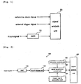
- FIG. 1 is a block diagram showing the construction of a conventional signal analyzer.
- a signal analysis unit 20 receives an input signal that is converted in digital form via an Analog-to-Digital Converter (ADC) 10, and receives reference clock signals and external trigger signals from the outside, that is, from the transmitter that transmitted the input signal, in order to analyze the input signal.
- the external trigger signals are signals that are used to acquire the synchronization of the input signal, and are signals that are input in conformity with the respective start positions of frames that constitute the input signal.
- Each of the reference clock signals is a signal that is input for use as a reference clock when various types of clocks to be used in a system are generated. That is, the signal analysis unit 20 analyzes a given number of frames of the input signal based on the external trigger signals and the reference clock signals.
- the synchronization of the input signal cannot be acquired in an environment in which the external trigger signals cannot be received, for example, in a mobile communication base station, and thus there is a problem in that accurate signal analysis cannot be performed.
- each frame can be calculated by installing a synchronization acquisition algorithm in the signal analyzer itself, rather than using the external trigger signals.
- each of the calculation intervals for synchronization acquisition is longer than a single frame, so that it takes a lot of time to acquire the synchronization of the input signal, therefore a problem exists in that the usefulness of the signal analyzer is limited.
- EP 0 981 054 A2 is considered as closest prior art forming the basis for the preamble of independent claims 1 and 3.
- EP 0 969 608 A2 discloses a channel estimation device for digital telecommunication stations.
- Said device comprises a first channel estimation means providing a time error estimate in accordance with the correlation between a central group of bits of a received training sequence with the corresponding bits of an expected training sequence, an averaging means to average each bit of a first subgroup to a corresponding bit of a second subgroup and a second estimator means operating to recalculate the timing error estimate.
- US 2005/0 282 568 A1 discloses a time synchronisation method in a communication system by use of spectral estimation.
- a receiver obtains a frequency response estimate for pilot symbols received on each set of frequency subbands used for pilot transmission.
- the receiver obtains a measured arrival time for a transmission from a transmitter.
- a time error between a measured arrival time and a desired arrival time is computed, and a time adjustment is then generated using linear or non-linear functions. The time adjustment is used to adjust the transmit timing at the transmitter.
- an object of the present invention is to provide an apparatus and method for synchronizing a signal analyzer, which internally generates a trigger signal, which is used as a reference point for signal acquisition, for each predetermined period, and enables both the acquisition of synchronization and tracking to be performed on the basis of the trigger signal.
- the present invention provides an apparatus for synchronizing a signal analyzer, the apparatus being applied to the signal analyzer for analyzing an input signal, the input signal being input from outside and having a frame structure, the apparatus including an Analog-to-Digital Converter (ADC) for converting the input signal into a corresponding digital signal; a signal storage unit for storing the digital signal received from the ADC; a trigger signal generation unit for generating a trigger signal for each predetermined period; a signal acquisition control unit for acquiring the digital signal, stored in the signal storage unit, from a signal acquisition time point that is preset on the basis of a trigger signal received from the trigger signal generation unit; a signal analysis unit for calculating the start position of a frame from the digital signal, which is received from the signal acquisition control unit; and a time error control unit for calculating a time error between the time point at which each trigger signal is generated and the start position of the digital signal in consideration of the start position, which is calculated by the signal analysis unit, and a clock error between a transmitter,
- ADC Analog-
- the present invention provides a method of synchronizing a signal analyzer, the method being performed in the signal analyzer for analyzing an input signal, the input signal being input from an outside and having a frame structure, the method including the steps of (a) converting the input signal into a digital signal; (b) storing the digital signal; (c) generating trigger signals for respective predetermined periods; (d) acquiring the digital signal, which is stored at the step (b), from an arbitrary time point on the basis of the time point at which each trigger signal is generated; (e) calculating the start position of a frame from the digital signal acquired at step (d); and (f) setting an acquisition time point for the digital signal acquired at step (d), based on the start position of each frame calculated at the step (e).
- FIG. 2 is a block diagram showing the construction of an apparatus for synchronizing a signal analyzer according to an embodiment of the present invention.
- the apparatus 100 for synchronizing a signal analyzer includes an ADC 110 for converting an analog input signal into a digital signal, a signal storage unit 140 for storing the digital signal received from the ADC 110, a trigger signal generation unit 150 for generating a trigger signal, which is used as a reference point for signal acquisition for each predetermined period, for example, for a period of 5 ⁇ , which corresponds to a single frame of a Wireless Broadband (WiBro) system developed by South Korea, a signal acquisition control unit 120 for acquiring the signal of the signal storage unit 140 from a 'signal acquisition time point,' which is preset on the basis of a trigger signal received from the trigger signal generation unit 150, a signal analysis unit 160 for calculating the start position of a frame from the digital signal, which is received from the signal acquisition control unit 120, and analyzing the frame, and a time error control unit 130 for calculating a 'time error' between the time point at which each trigger signal is generated and the start position of a the digital signal in
- the time error control unit 130 sets a signal acquisition time point for each frame.
- the signal acquisition control unit 120 acquires the signal of the signal storage unit 140 from the signal acquisition time point, which is set by the time error control unit 130, based on the trigger signal received from the trigger signal generation unit 150.
- a tracking process of acquiring the synchronization of an input signal is performed between the time error control unit 130 and the signal acquisition control unit 120.
- the signal analysis unit 160 can rapidly perform the acquisition of synchronization and tracking on the digital signal, which is input from the signal acquisition control unit 120, through the tracking process.
- the signal analysis unit 160 includes a synchronization acquisition algorithm for calculating the start location of a frame received from the signal acquisition control unit 120, a series of algorithms for signal analysis, and a part for transmitting a signal acquisition command to the signal acquisition control unit 120 to read data to be analyzed.
- the time error control unit 130 includes a part for notifying the signal acquisition control unit 120 of the start position from which the next frame is acquired based on the set 'signal acquisition time point.' Accordingly, when a signal acquisition command is received from the signal analysis unit 160, the signal acquisition control unit 120 outputs the data of the signal storage unit 140 to the signal analysis unit 160 from the start position, which is received from the time error control unit 130, on the basis of a trigger signal corresponding to this command.
- the apparatus 100 for synchronizing a signal analyzer be applied to a Time Division Duplexing (TDD) system, which transmits and receives signals in a duplex manner, or an Orthogonal Frequency Division Multiple (OFDM) system, which transmits and receives signals in a multiple access manner.
- TDD Time Division Duplexing
- OFDM Orthogonal Frequency Division Multiple
- FIG. 3 is a chart showing the structure of transmission frames in an OFDM-based WiBro system.
- data information is represented in the time domain (transversal axis) and in the frequency domain (longitudinal axis).
- An uplink region and a downlink region, that is, a left region and a right region, are distinguished from each other using the time, as shown in the drawing.
- the uplink region may be divided into a preamble section, a Frame Control Header (FCH) section, a DownLink-MAP (DL-MAP) section, an UpLink-MAP (UL-MAP) section, and a data transmission section.
- data transmitted during the preamble section includes a signal for synchronization and a signal for cell division, and is information that must be first considered when a WiBro terminal receives data.
- codes that are transmitted in the preamble section are classified into a total of 114 types. The WiBro terminal selects the preamble code having the highest correlation from among the 114 preamble codes and then uses information of the selected preamble code, so that it can access the FCH section.
- data in the FCH section includes information that is necessary to demodulate the DL-MAP data, such as the method that is used to modulate the data of DL-MAP and the encoding method that is used.
- the DL-MAP data designates a data section and a modulation method, which are assigned to each WiBro terminal in the UL-MAP section and the data transmission section.
- the DL-MAP data includes information about the IDentification (ID) number of a base station selected by the WiBro terminal.
- FIG. 4 is a flowchart illustrating a method of synchronizing a signal analyzer according to an embodiment of the present invention
- FIG. 5 is a diagram showing an example of signal waveforms for illustrating a process of synchronizing an input signal based on the present invention.
- the ADC 110 converts an analog input signal into a digital signal and then outputs the digital signal, and at step 13, the trigger signal generation unit 150 generates a trigger signal for each predetermined period, for example, for a period of 5 ⁇ , which is the period of the input signal.
- the signal acquisition control unit 120 acquires the signal, which is stored in the storage unit 140, by a desired length from a 'signal acquisition time point,' which is preset on the basis of a corresponding input trigger signal, and outputs the acquired signal to the signal analysis unit 160.
- the signal analysis unit 160 calculates the start position of a frame from the digital signal, which is received from the signal acquisition control unit 120, based on an installed synchronization acquisition algorithm. For example, in the case where the input signal is a frame that is transmitted from the WiBro system, the signal analysis unit 160 detects a preamble section from the digital signal, which is received from the signal acquisition control unit 120, on the basis of the time point at which each trigger signal is generated.
- the time error control unit 130 sets a 'signal acquisition time point,' which will be applied at the time of acquiring the next frame signal, using a time value for which a clock error, which may occur between the transmitter and the receiver for which clock synchronization is not performed, and the start position of the frame, which is calculated at step S17, are considered. That is, as shown in FIG. 5 , the time error control unit 130 obtains the time error 't', which is generated due to mismatching between the start position of the trigger signal and the start position of the digital signal.
- the signal acquisition control unit 140 acquires the signal of the signal storage unit 140 by a desired length from the 'signal acquisition time point,' which is set at step S19, on the basis of the input trigger signal, and outputs the acquired signal to the signal analysis unit 160. Accordingly, the signal analysis unit 160 can perform the acquisition of synchronization and tracking without receiving the trigger signal or a reference clock signal from the outside.
- the apparatus and method for synchronizing a signal analyzer according to the present invention is not limited only to the above-described embodiments, and may be modified and implemented in various ways within the range permitted by the technological spirit of the present invention.
- the range of use of the signal analyzer is widened due to the effect in which a trigger signal is internally generated for each predetermined period and the input signal seems to be synchronized with the trigger signals. That is, the present invention is appropriate for a wireless environment, so that it has an effect in that signal analysis can be performed regardless of place and time using only the signal analyzer, rather than using any external trigger signal or any clock synchronization signal.
- the signal analysis unit receives the digital signal from the signal acquisition control unit from a location for which the start position of each preamble is considered, so that the calculation time necessary for the acquisition of synchronization is greatly reduced, therefore the signal analysis unit can directly analyze the input digital signal.
- tracking can be performed while maintaining synchronization time without receiving the trigger signal or the reference clock signal from the outside, through a process of setting a time error value, which will be applied at the time of acquiring the next frame signal using a time value, for which a clock error, which may occur between the transmitter and the receiver on which clock synchronization is not performed, and the start value of the preamble are considered.
Landscapes
- Physics & Mathematics (AREA)
- General Physics & Mathematics (AREA)
- Mathematical Physics (AREA)
- Engineering & Computer Science (AREA)
- Computer Networks & Wireless Communication (AREA)
- Signal Processing (AREA)
- Synchronisation In Digital Transmission Systems (AREA)
- Time-Division Multiplex Systems (AREA)
- Analogue/Digital Conversion (AREA)
Abstract
Description
- The present invention relates generally to an apparatus and method for synchronizing a signal analyzer and, more particularly, to an apparatus and method for synchronizing a signal analyzer, which, when the signal analyzer analyzes a signal input from the outside, can achieve the synchronization of the input signal in a short period without receiving a trigger signal from the outside.
- Generally, the term 'signal analyzer' refers to a measuring instrument that resolves the frequencies of an arbitrary input signal into sine waves and analyzes the components thereof, and may be classified as a spectrum analyzer, a network analyzer, a digital analyzer, a frequency analyzer and a wave analyzer according to the purpose of use.
-
FIG. 1 is a block diagram showing the construction of a conventional signal analyzer. - As shown in
FIG. 1 , asignal analysis unit 20 receives an input signal that is converted in digital form via an Analog-to-Digital Converter (ADC) 10, and receives reference clock signals and external trigger signals from the outside, that is, from the transmitter that transmitted the input signal, in order to analyze the input signal. In this case, the external trigger signals are signals that are used to acquire the synchronization of the input signal, and are signals that are input in conformity with the respective start positions of frames that constitute the input signal. Each of the reference clock signals is a signal that is input for use as a reference clock when various types of clocks to be used in a system are generated. That is, thesignal analysis unit 20 analyzes a given number of frames of the input signal based on the external trigger signals and the reference clock signals. - However, in accordance with the conventional signal analyzer described above, the synchronization of the input signal cannot be acquired in an environment in which the external trigger signals cannot be received, for example, in a mobile communication base station, and thus there is a problem in that accurate signal analysis cannot be performed.
- Furthermore, the start position of each frame can be calculated by installing a synchronization acquisition algorithm in the signal analyzer itself, rather than using the external trigger signals. In this case, each of the calculation intervals for synchronization acquisition is longer than a single frame, so that it takes a lot of time to acquire the synchronization of the input signal, therefore a problem exists in that the usefulness of the signal analyzer is limited.
-
EP 0 981 054 A2 is considered as closest prior art forming the basis for the preamble of independent claims 1 and 3. - The article "DECT measurements with a microwave spectrum analyzer" by M.A.Elo published in the "Hewlett Packard Journal", vol. 44, no. 6 at December 1st, 1993, on pages 98 to 106, discloses a method similar to the method and apparatus discussed in above-mentioned
EP 0 981 054 A2 . -
EP 0 969 608 A2 discloses a channel estimation device for digital telecommunication stations. Said device comprises a first channel estimation means providing a time error estimate in accordance with the correlation between a central group of bits of a received training sequence with the corresponding bits of an expected training sequence, an averaging means to average each bit of a first subgroup to a corresponding bit of a second subgroup and a second estimator means operating to recalculate the timing error estimate. -
US 2005/0 282 568 A1 discloses a time synchronisation method in a communication system by use of spectral estimation. To this purpose a receiver obtains a frequency response estimate for pilot symbols received on each set of frequency subbands used for pilot transmission. The receiver obtains a measured arrival time for a transmission from a transmitter. A time error between a measured arrival time and a desired arrival time is computed, and a time adjustment is then generated using linear or non-linear functions. The time adjustment is used to adjust the transmit timing at the transmitter. - Accordingly, the present invention has been made keeping in mind the above problems occurring in the prior art, and an object of the present invention is to provide an apparatus and method for synchronizing a signal analyzer, which internally generates a trigger signal, which is used as a reference point for signal acquisition, for each predetermined period, and enables both the acquisition of synchronization and tracking to be performed on the basis of the trigger signal.
- In order to accomplish the above object, the present invention provides an apparatus for synchronizing a signal analyzer, the apparatus being applied to the signal analyzer for analyzing an input signal, the input signal being input from outside and having a frame structure, the apparatus including an Analog-to-Digital Converter (ADC) for converting the input signal into a corresponding digital signal; a signal storage unit for storing the digital signal received from the ADC; a trigger signal generation unit for generating a trigger signal for each predetermined period; a signal acquisition control unit for acquiring the digital signal, stored in the signal storage unit, from a signal acquisition time point that is preset on the basis of a trigger signal received from the trigger signal generation unit; a signal analysis unit for calculating the start position of a frame from the digital signal, which is received from the signal acquisition control unit; and a time error control unit for calculating a time error between the time point at which each trigger signal is generated and the start position of the digital signal in consideration of the start position, which is calculated by the signal analysis unit, and a clock error between a transmitter, which is used to transmit the input signal, and the signal analyzer, and setting a subsequent signal acquisition time point based on the calculated time errors. In this case, the apparatus for synchronizing a signal analyzer is applied to a Time Division Duplexing (TDD) system.
- In addition, the present invention provides a method of synchronizing a signal analyzer, the method being performed in the signal analyzer for analyzing an input signal, the input signal being input from an outside and having a frame structure, the method including the steps of (a) converting the input signal into a digital signal; (b) storing the digital signal; (c) generating trigger signals for respective predetermined periods; (d) acquiring the digital signal, which is stored at the step (b), from an arbitrary time point on the basis of the time point at which each trigger signal is generated; (e) calculating the start position of a frame from the digital signal acquired at step (d); and (f) setting an acquisition time point for the digital signal acquired at step (d), based on the start position of each frame calculated at the step (e).
- The above and other objects, features and advantages of the present invention will be more clearly understood from the following detailed description taken in conjunction with the accompanying drawings, in which:
-
FIG. 1 is a block diagram showing the construction of a conventional signal analyzer; -
FIG. 2 is a block diagram showing the construction of an apparatus for synchronizing a signal analyzer according to an embodiment of the present invention; -
FIG. 3 is a chart showing the structure of transmission frames in an OFDM-based WiBro system; -
FIG. 4 is a flowchart illustrating a method of synchronizing a signal analyzer according to an embodiment of the present invention; and -
FIG. 5 is a diagram showing an example of signal waveforms for illustrating a process of synchronizing an input signal based on the present invention. - The apparatus and method for synchronizing a signal analyzer according to preferred embodiments of the present invention are described in detail with reference to the accompanying drawings below.
-
FIG. 2 is a block diagram showing the construction of an apparatus for synchronizing a signal analyzer according to an embodiment of the present invention. - As shown in
FIG. 2 , theapparatus 100 for synchronizing a signal analyzer includes anADC 110 for converting an analog input signal into a digital signal, asignal storage unit 140 for storing the digital signal received from theADC 110, a triggersignal generation unit 150 for generating a trigger signal, which is used as a reference point for signal acquisition for each predetermined period, for example, for a period of 5 □, which corresponds to a single frame of a Wireless Broadband (WiBro) system developed by South Korea, a signalacquisition control unit 120 for acquiring the signal of thesignal storage unit 140 from a 'signal acquisition time point,' which is preset on the basis of a trigger signal received from the triggersignal generation unit 150, asignal analysis unit 160 for calculating the start position of a frame from the digital signal, which is received from the signalacquisition control unit 120, and analyzing the frame, and a timeerror control unit 130 for calculating a 'time error' between the time point at which each trigger signal is generated and the start position of a the digital signal in consideration of the start position, which is received from thesignal analysis unit 160, and a clock error, which may occur between a transmitter and a receiver, and setting a 'signal acquisition time point,' which will be applied at the time of acquiring the next frame, based on the calculated time error. That is, the timeerror control unit 130 sets a signal acquisition time point for each frame. The signalacquisition control unit 120 acquires the signal of thesignal storage unit 140 from the signal acquisition time point, which is set by the timeerror control unit 130, based on the trigger signal received from the triggersignal generation unit 150. In this manner, a tracking process of acquiring the synchronization of an input signal is performed between the timeerror control unit 130 and the signalacquisition control unit 120. Accordingly, thesignal analysis unit 160 can rapidly perform the acquisition of synchronization and tracking on the digital signal, which is input from the signalacquisition control unit 120, through the tracking process. - In the above-described construction, the
signal analysis unit 160 includes a synchronization acquisition algorithm for calculating the start location of a frame received from the signalacquisition control unit 120, a series of algorithms for signal analysis, and a part for transmitting a signal acquisition command to the signalacquisition control unit 120 to read data to be analyzed. The timeerror control unit 130 includes a part for notifying the signalacquisition control unit 120 of the start position from which the next frame is acquired based on the set 'signal acquisition time point.' Accordingly, when a signal acquisition command is received from thesignal analysis unit 160, the signalacquisition control unit 120 outputs the data of thesignal storage unit 140 to thesignal analysis unit 160 from the start position, which is received from the timeerror control unit 130, on the basis of a trigger signal corresponding to this command. - Here, it is preferred that the
apparatus 100 for synchronizing a signal analyzer be applied to a Time Division Duplexing (TDD) system, which transmits and receives signals in a duplex manner, or an Orthogonal Frequency Division Multiple (OFDM) system, which transmits and receives signals in a multiple access manner. -
FIG. 3 is a chart showing the structure of transmission frames in an OFDM-based WiBro system. As shown inFIG. 3 , in the OFDM-based WiBro system, data information is represented in the time domain (transversal axis) and in the frequency domain (longitudinal axis). An uplink region and a downlink region, that is, a left region and a right region, are distinguished from each other using the time, as shown in the drawing. - In the above-described structure, the uplink region may be divided into a preamble section, a Frame Control Header (FCH) section, a DownLink-MAP (DL-MAP) section, an UpLink-MAP (UL-MAP) section, and a data transmission section. In this case, data transmitted during the preamble section includes a signal for synchronization and a signal for cell division, and is information that must be first considered when a WiBro terminal receives data. According to a standard, codes that are transmitted in the preamble section are classified into a total of 114 types. The WiBro terminal selects the preamble code having the highest correlation from among the 114 preamble codes and then uses information of the selected preamble code, so that it can access the FCH section.
- Subsequently, data in the FCH section includes information that is necessary to demodulate the DL-MAP data, such as the method that is used to modulate the data of DL-MAP and the encoding method that is used. In contrast, the DL-MAP data designates a data section and a modulation method, which are assigned to each WiBro terminal in the UL-MAP section and the data transmission section. In addition, the DL-MAP data includes information about the IDentification (ID) number of a base station selected by the WiBro terminal.
-
FIG. 4 is a flowchart illustrating a method of synchronizing a signal analyzer according to an embodiment of the present invention, andFIG. 5 is a diagram showing an example of signal waveforms for illustrating a process of synchronizing an input signal based on the present invention. - First, at step S11, the ADC 110 converts an analog input signal into a digital signal and then outputs the digital signal, and at step 13, the trigger
signal generation unit 150 generates a trigger signal for each predetermined period, for example, for a period of 5 □, which is the period of the input signal. - Thereafter, at step S15, the signal
acquisition control unit 120 acquires the signal, which is stored in thestorage unit 140, by a desired length from a 'signal acquisition time point,' which is preset on the basis of a corresponding input trigger signal, and outputs the acquired signal to thesignal analysis unit 160. - Thereafter, at step S17, the
signal analysis unit 160 calculates the start position of a frame from the digital signal, which is received from the signalacquisition control unit 120, based on an installed synchronization acquisition algorithm. For example, in the case where the input signal is a frame that is transmitted from the WiBro system, thesignal analysis unit 160 detects a preamble section from the digital signal, which is received from the signalacquisition control unit 120, on the basis of the time point at which each trigger signal is generated. - Thereafter, at step S19, the time
error control unit 130 sets a 'signal acquisition time point,' which will be applied at the time of acquiring the next frame signal, using a time value for which a clock error, which may occur between the transmitter and the receiver for which clock synchronization is not performed, and the start position of the frame, which is calculated at step S17, are considered. That is, as shown inFIG. 5 , the timeerror control unit 130 obtains the time error 't', which is generated due to mismatching between the start position of the trigger signal and the start position of the digital signal. - Accordingly, the signal
acquisition control unit 140 acquires the signal of thesignal storage unit 140 by a desired length from the 'signal acquisition time point,' which is set at step S19, on the basis of the input trigger signal, and outputs the acquired signal to thesignal analysis unit 160. Accordingly, thesignal analysis unit 160 can perform the acquisition of synchronization and tracking without receiving the trigger signal or a reference clock signal from the outside. - The apparatus and method for synchronizing a signal analyzer according to the present invention is not limited only to the above-described embodiments, and may be modified and implemented in various ways within the range permitted by the technological spirit of the present invention.
- As described above, in accordance with the apparatus and method for synchronizing a signal analyzer according to the present invention, the range of use of the signal analyzer is widened due to the effect in which a trigger signal is internally generated for each predetermined period and the input signal seems to be synchronized with the trigger signals. That is, the present invention is appropriate for a wireless environment, so that it has an effect in that signal analysis can be performed regardless of place and time using only the signal analyzer, rather than using any external trigger signal or any clock synchronization signal.
- Furthermore, the signal analysis unit receives the digital signal from the signal acquisition control unit from a location for which the start position of each preamble is considered, so that the calculation time necessary for the acquisition of synchronization is greatly reduced, therefore the signal analysis unit can directly analyze the input digital signal.
- In addition, when each frame is analyzed by the time error control unit, tracking can be performed while maintaining synchronization time without receiving the trigger signal or the reference clock signal from the outside, through a process of setting a time error value, which will be applied at the time of acquiring the next frame signal using a time value, for which a clock error, which may occur between the transmitter and the receiver on which clock synchronization is not performed, and the start value of the preamble are considered.
Claims (3)
- An apparatus (100) for synchronizing a signal analyzer, the apparatus (100) comprising:an Analog-to-Digital Converter (110) for converting an input signal being input from the outside and having a frame structure into a corresponding digital signal;a signal storage unit (140) for storing the digital signal received from the Analog-to-Digital Converter (110); characterized by further comprisinga trigger signal generation unit (150) for generating a trigger signal for each predetermined period;a signal acquisition control unit (120) for acquiring the digital signal, stored in the signal storage unit (140), from a signal acquisition time point that is preset on a basis of a trigger signal received from the trigger signal generation unit (150) by a desired length from the signal acquisition time point;signal analysis means (160) for calculating a start position of a frame from the digital signal, which is received from the signal acquisition control unit (120); anda time error control unit (130) for calculating a time error between a time point at which each trigger signal is generated and the start position of the frame, which is calculated by the signal analysis means (160), and setting a subsequent signal acquisition time point based on the calculated time error.
- The apparatus (100) as set forth in claim 1, wherein the apparatus (100) for synchronizing a signal analyzer is applied to a Time Division Duplexing system.
- A method of synchronizing a signal analyzer, the method comprising the steps of:(a) converting an input signal being input from the outside and having a frame structure into a corresponding digital signal;(b) storing the digital signal;
the method characterized by further comprising the steps of(c) generating a trigger signal for each predetermined period;(d) acquiring the digital signal, which is stored at step (b), from a signal acquisition time point that is preset on a basis of the trigger signal which is generated at step (c) by a desired length from the signal acquisition time point;(e) calculating a start position of a frame from the digital signal acquired at step (d); and(f) calculating a time error between a time point at which each trigger signal is generated and the start position of the frame which is calculated at step (e), and setting a subsequent signal acquisition time point based on the calculated time error.
Applications Claiming Priority (1)
| Application Number | Priority Date | Filing Date | Title |
|---|---|---|---|
| KR1020060073018A KR100791823B1 (en) | 2006-08-02 | 2006-08-02 | Synchronization Device and Method of Signal Analyzer |
Publications (2)
| Publication Number | Publication Date |
|---|---|
| EP1885080A1 EP1885080A1 (en) | 2008-02-06 |
| EP1885080B1 true EP1885080B1 (en) | 2011-09-28 |
Family
ID=38556393
Family Applications (1)
| Application Number | Title | Priority Date | Filing Date |
|---|---|---|---|
| EP07015119A Active EP1885080B1 (en) | 2006-08-02 | 2007-08-01 | Apparatus and method for synchronizing signal analyzer |
Country Status (5)
| Country | Link |
|---|---|
| US (1) | US8130884B2 (en) |
| EP (1) | EP1885080B1 (en) |
| JP (1) | JP5086712B2 (en) |
| KR (1) | KR100791823B1 (en) |
| AT (1) | ATE526749T1 (en) |
Cited By (1)
| Publication number | Priority date | Publication date | Assignee | Title |
|---|---|---|---|---|
| US10965441B1 (en) | 2019-10-10 | 2021-03-30 | Rohde & Schwarz Gmbh & Co. Kg | Frame trigger recreation method and frame trigger recreator |
Families Citing this family (7)
| Publication number | Priority date | Publication date | Assignee | Title |
|---|---|---|---|---|
| KR100765818B1 (en) * | 2006-05-08 | 2007-10-10 | 주식회사 이노와이어리스 | Signal quality measuring device and method of portable internet system |
| US8223820B2 (en) * | 2007-12-31 | 2012-07-17 | Silicon Laboratories Inc. | Method and apparatus for symbol synchronization for an 802.15.4 radio platform |
| CN104635047B (en) * | 2013-11-08 | 2019-01-08 | 苏州普源精电科技有限公司 | A kind of spectrum analyzer with calibration function |
| US10798668B2 (en) | 2016-03-28 | 2020-10-06 | Anritsu Corporation | Synchronization circuit, synchronization method, signal generating device, signal generating method, and recording medium |
| JP6473429B2 (en) * | 2016-03-30 | 2019-02-20 | アンリツ株式会社 | Synchronization circuit and synchronization method |
| KR101768392B1 (en) | 2016-09-27 | 2017-08-16 | (주) 소암컨설턴트 | Microearthquake measuring system and method improved the accuracy of time synchronization |
| JP7372950B2 (en) * | 2021-03-17 | 2023-11-01 | アンリツ株式会社 | Signal analysis device and signal analysis result display method |
Family Cites Families (13)
| Publication number | Priority date | Publication date | Assignee | Title |
|---|---|---|---|---|
| JP2778191B2 (en) * | 1990-03-27 | 1998-07-23 | ソニー株式会社 | TV camera with integrated recording device |
| US5162723A (en) * | 1991-02-11 | 1992-11-10 | Hewlett-Packard Company | Sampling signal analyzer |
| DE4231175C1 (en) * | 1992-09-17 | 1994-01-13 | Siemens Ag | Arrangement for clock recovery |
| KR960013758B1 (en) * | 1994-08-26 | 1996-10-10 | 엘지전자 주식회사 | External synchronous circuit for chip test |
| JP3359251B2 (en) * | 1996-12-11 | 2002-12-24 | ソニー・テクトロニクス株式会社 | Real-time signal analyzer |
| GB2339120B (en) * | 1998-06-30 | 2003-03-19 | Nec Technologies | Channel estimation device for digital telecommunications stations |
| US6356067B1 (en) | 1998-08-10 | 2002-03-12 | Sony/Tektronix Corporation | Wide band signal analyzer with wide band and narrow band signal processors |
| JP3431544B2 (en) * | 1998-08-10 | 2003-07-28 | テクトロニクス・インターナショナル・セールス・ゲーエムベーハー | Wideband signal analyzer |
| KR100358371B1 (en) * | 2000-10-12 | 2002-10-25 | 엘지이노텍 주식회사 | A Control Signal Generating Device and A Method |
| US7106709B2 (en) * | 2000-11-29 | 2006-09-12 | Telefonaktiebologet Lm Ericsson (Publ) | Timing drift compensation in wireless packet-based systems |
| US7492828B2 (en) * | 2004-06-18 | 2009-02-17 | Qualcomm Incorporated | Time synchronization using spectral estimation in a communication system |
| US7225093B1 (en) * | 2005-11-21 | 2007-05-29 | Agilent Technologies, Inc. | System and method for generating triggers based on predetermined trigger waveform and a measurement signal |
| US7480839B2 (en) * | 2005-12-08 | 2009-01-20 | Tektronix, Inc. | Qualified anomaly detection |
-
2006
- 2006-08-02 KR KR1020060073018A patent/KR100791823B1/en active Active
-
2007
- 2007-07-11 JP JP2007182303A patent/JP5086712B2/en active Active
- 2007-08-01 EP EP07015119A patent/EP1885080B1/en active Active
- 2007-08-01 AT AT07015119T patent/ATE526749T1/en not_active IP Right Cessation
- 2007-08-02 US US11/832,706 patent/US8130884B2/en active Active
Cited By (1)
| Publication number | Priority date | Publication date | Assignee | Title |
|---|---|---|---|---|
| US10965441B1 (en) | 2019-10-10 | 2021-03-30 | Rohde & Schwarz Gmbh & Co. Kg | Frame trigger recreation method and frame trigger recreator |
Also Published As
| Publication number | Publication date |
|---|---|
| JP2008042898A (en) | 2008-02-21 |
| EP1885080A1 (en) | 2008-02-06 |
| KR100791823B1 (en) | 2008-01-04 |
| US8130884B2 (en) | 2012-03-06 |
| ATE526749T1 (en) | 2011-10-15 |
| US20080031392A1 (en) | 2008-02-07 |
| JP5086712B2 (en) | 2012-11-28 |
Similar Documents
| Publication | Publication Date | Title |
|---|---|---|
| EP0829988B1 (en) | Symbol synchronization and sampling frequency adjustment in an OFDM receiver | |
| CN102089997B (en) | Signal transmission parameter control using channel sounding | |
| US8130884B2 (en) | Apparatus and method for synchronizing signal analyzer | |
| US7321563B2 (en) | Apparatus and method for estimating a channel condition of a forward link in a mobile communication system | |
| US6700875B1 (en) | System, device, and method for selecting a channel in a multichannel communication network | |
| AU656487B2 (en) | Method and apparatus of estimating channel quality in a receiver | |
| US20090003494A1 (en) | Radio communication system and apparatus | |
| KR20100051787A (en) | Terminal device and base station device | |
| KR20020020792A (en) | Method and apparatus for sequentially synchronized network | |
| EP2088688B1 (en) | Technique for performing a random access procedure in a mobile device | |
| JPH11275035A (en) | Mobile station communication device, base station communication device, and wireless communication system | |
| US20170214477A1 (en) | Method of calibrating power for mimo-ofdm transmitter | |
| EP2066068A1 (en) | Receiving apparatus, communication system, receiving method and program | |
| EP0931390B1 (en) | Improved synchronization of a receiver with a transmitter using nonlinear transformation metrics | |
| CN100401655C (en) | Device and method for adjusting transmission time of continuous transmission signal | |
| JP2002368664A (en) | Communication apparatus and transmission array antenna calibration method thereof | |
| JP2021083009A (en) | Adaptive equalizer, optical receiver using the same, and optical transfer system | |
| US20110053629A1 (en) | Base station apparatus, antenna device, terminal device, communication system, and communication method | |
| US20080032651A1 (en) | Relay For Multi-Carrier Wireless Communications System | |
| JP2006279901A (en) | Communication device and calibration weight estimation method | |
| KR200425602Y1 (en) | Automatic Gain Control Device and Transceiver in Wireless Communication System Using TD System | |
| JPH01133441A (en) | Clock synchronizing system | |
| KR101031874B1 (en) | How to Synchronize Data in Wireless Communication Devices Using Short Wave Frequencies | |
| JPH11163779A (en) | Radio equipment | |
| HK1119330A (en) | Automatic frequency offset compensation in a tdd wireless ofdm communication system |
Legal Events
| Date | Code | Title | Description |
|---|---|---|---|
| PUAI | Public reference made under article 153(3) epc to a published international application that has entered the european phase |
Free format text: ORIGINAL CODE: 0009012 |
|
| AK | Designated contracting states |
Kind code of ref document: A1 Designated state(s): AT BE BG CH CY CZ DE DK EE ES FI FR GB GR HU IE IS IT LI LT LU LV MC MT NL PL PT RO SE SI SK TR |
|
| AX | Request for extension of the european patent |
Extension state: AL BA HR MK YU |
|
| 17P | Request for examination filed |
Effective date: 20080527 |
|
| 17Q | First examination report despatched |
Effective date: 20080626 |
|
| AKX | Designation fees paid |
Designated state(s): AT BE BG CH CY CZ DE DK EE ES FI FR GB GR HU IE IS IT LI LT LU LV MC MT NL PL PT RO SE SI SK TR |
|
| GRAP | Despatch of communication of intention to grant a patent |
Free format text: ORIGINAL CODE: EPIDOSNIGR1 |
|
| GRAS | Grant fee paid |
Free format text: ORIGINAL CODE: EPIDOSNIGR3 |
|
| RIN1 | Information on inventor provided before grant (corrected) |
Inventor name: PARK, JUNWAN Inventor name: HA, KYEONGMIN Inventor name: JOUNG, JINSOUP Inventor name: JANG, BYUNGKWAN |
|
| GRAA | (expected) grant |
Free format text: ORIGINAL CODE: 0009210 |
|
| AK | Designated contracting states |
Kind code of ref document: B1 Designated state(s): AT BE BG CH CY CZ DE DK EE ES FI FR GB GR HU IE IS IT LI LT LU LV MC MT NL PL PT RO SE SI SK TR |
|
| REG | Reference to a national code |
Ref country code: GB Ref legal event code: FG4D |
|
| REG | Reference to a national code |
Ref country code: CH Ref legal event code: EP |
|
| REG | Reference to a national code |
Ref country code: IE Ref legal event code: FG4D |
|
| REG | Reference to a national code |
Ref country code: DE Ref legal event code: R096 Ref document number: 602007017456 Country of ref document: DE Effective date: 20111124 |
|
| REG | Reference to a national code |
Ref country code: NL Ref legal event code: VDEP Effective date: 20110928 |
|
| PG25 | Lapsed in a contracting state [announced via postgrant information from national office to epo] |
Ref country code: FI Free format text: LAPSE BECAUSE OF FAILURE TO SUBMIT A TRANSLATION OF THE DESCRIPTION OR TO PAY THE FEE WITHIN THE PRESCRIBED TIME-LIMIT Effective date: 20110928 Ref country code: SE Free format text: LAPSE BECAUSE OF FAILURE TO SUBMIT A TRANSLATION OF THE DESCRIPTION OR TO PAY THE FEE WITHIN THE PRESCRIBED TIME-LIMIT Effective date: 20110928 Ref country code: LT Free format text: LAPSE BECAUSE OF FAILURE TO SUBMIT A TRANSLATION OF THE DESCRIPTION OR TO PAY THE FEE WITHIN THE PRESCRIBED TIME-LIMIT Effective date: 20110928 |
|
| LTIE | Lt: invalidation of european patent or patent extension |
Effective date: 20110928 |
|
| PG25 | Lapsed in a contracting state [announced via postgrant information from national office to epo] |
Ref country code: GR Free format text: LAPSE BECAUSE OF FAILURE TO SUBMIT A TRANSLATION OF THE DESCRIPTION OR TO PAY THE FEE WITHIN THE PRESCRIBED TIME-LIMIT Effective date: 20111229 Ref country code: AT Free format text: LAPSE BECAUSE OF FAILURE TO SUBMIT A TRANSLATION OF THE DESCRIPTION OR TO PAY THE FEE WITHIN THE PRESCRIBED TIME-LIMIT Effective date: 20110928 Ref country code: CY Free format text: LAPSE BECAUSE OF FAILURE TO SUBMIT A TRANSLATION OF THE DESCRIPTION OR TO PAY THE FEE WITHIN THE PRESCRIBED TIME-LIMIT Effective date: 20110928 Ref country code: SI Free format text: LAPSE BECAUSE OF FAILURE TO SUBMIT A TRANSLATION OF THE DESCRIPTION OR TO PAY THE FEE WITHIN THE PRESCRIBED TIME-LIMIT Effective date: 20110928 Ref country code: LV Free format text: LAPSE BECAUSE OF FAILURE TO SUBMIT A TRANSLATION OF THE DESCRIPTION OR TO PAY THE FEE WITHIN THE PRESCRIBED TIME-LIMIT Effective date: 20110928 |
|
| REG | Reference to a national code |
Ref country code: AT Ref legal event code: MK05 Ref document number: 526749 Country of ref document: AT Kind code of ref document: T Effective date: 20110928 |
|
| PG25 | Lapsed in a contracting state [announced via postgrant information from national office to epo] |
Ref country code: BE Free format text: LAPSE BECAUSE OF FAILURE TO SUBMIT A TRANSLATION OF THE DESCRIPTION OR TO PAY THE FEE WITHIN THE PRESCRIBED TIME-LIMIT Effective date: 20110928 |
|
| PG25 | Lapsed in a contracting state [announced via postgrant information from national office to epo] |
Ref country code: SK Free format text: LAPSE BECAUSE OF FAILURE TO SUBMIT A TRANSLATION OF THE DESCRIPTION OR TO PAY THE FEE WITHIN THE PRESCRIBED TIME-LIMIT Effective date: 20110928 Ref country code: CZ Free format text: LAPSE BECAUSE OF FAILURE TO SUBMIT A TRANSLATION OF THE DESCRIPTION OR TO PAY THE FEE WITHIN THE PRESCRIBED TIME-LIMIT Effective date: 20110928 Ref country code: IS Free format text: LAPSE BECAUSE OF FAILURE TO SUBMIT A TRANSLATION OF THE DESCRIPTION OR TO PAY THE FEE WITHIN THE PRESCRIBED TIME-LIMIT Effective date: 20120128 |
|
| PG25 | Lapsed in a contracting state [announced via postgrant information from national office to epo] |
Ref country code: IT Free format text: LAPSE BECAUSE OF FAILURE TO SUBMIT A TRANSLATION OF THE DESCRIPTION OR TO PAY THE FEE WITHIN THE PRESCRIBED TIME-LIMIT Effective date: 20110928 Ref country code: NL Free format text: LAPSE BECAUSE OF FAILURE TO SUBMIT A TRANSLATION OF THE DESCRIPTION OR TO PAY THE FEE WITHIN THE PRESCRIBED TIME-LIMIT Effective date: 20110928 Ref country code: PT Free format text: LAPSE BECAUSE OF FAILURE TO SUBMIT A TRANSLATION OF THE DESCRIPTION OR TO PAY THE FEE WITHIN THE PRESCRIBED TIME-LIMIT Effective date: 20120130 Ref country code: EE Free format text: LAPSE BECAUSE OF FAILURE TO SUBMIT A TRANSLATION OF THE DESCRIPTION OR TO PAY THE FEE WITHIN THE PRESCRIBED TIME-LIMIT Effective date: 20110928 Ref country code: RO Free format text: LAPSE BECAUSE OF FAILURE TO SUBMIT A TRANSLATION OF THE DESCRIPTION OR TO PAY THE FEE WITHIN THE PRESCRIBED TIME-LIMIT Effective date: 20110928 |
|
| PG25 | Lapsed in a contracting state [announced via postgrant information from national office to epo] |
Ref country code: DK Free format text: LAPSE BECAUSE OF FAILURE TO SUBMIT A TRANSLATION OF THE DESCRIPTION OR TO PAY THE FEE WITHIN THE PRESCRIBED TIME-LIMIT Effective date: 20110928 |
|
| PLBE | No opposition filed within time limit |
Free format text: ORIGINAL CODE: 0009261 |
|
| STAA | Information on the status of an ep patent application or granted ep patent |
Free format text: STATUS: NO OPPOSITION FILED WITHIN TIME LIMIT |
|
| PG25 | Lapsed in a contracting state [announced via postgrant information from national office to epo] |
Ref country code: PL Free format text: LAPSE BECAUSE OF FAILURE TO SUBMIT A TRANSLATION OF THE DESCRIPTION OR TO PAY THE FEE WITHIN THE PRESCRIBED TIME-LIMIT Effective date: 20110928 |
|
| 26N | No opposition filed |
Effective date: 20120629 |
|
| REG | Reference to a national code |
Ref country code: DE Ref legal event code: R097 Ref document number: 602007017456 Country of ref document: DE Effective date: 20120629 |
|
| REG | Reference to a national code |
Ref country code: CH Ref legal event code: PL |
|
| PG25 | Lapsed in a contracting state [announced via postgrant information from national office to epo] |
Ref country code: MC Free format text: LAPSE BECAUSE OF NON-PAYMENT OF DUE FEES Effective date: 20120831 |
|
| GBPC | Gb: european patent ceased through non-payment of renewal fee |
Effective date: 20120801 |
|
| PG25 | Lapsed in a contracting state [announced via postgrant information from national office to epo] |
Ref country code: ES Free format text: LAPSE BECAUSE OF FAILURE TO SUBMIT A TRANSLATION OF THE DESCRIPTION OR TO PAY THE FEE WITHIN THE PRESCRIBED TIME-LIMIT Effective date: 20120108 Ref country code: LI Free format text: LAPSE BECAUSE OF NON-PAYMENT OF DUE FEES Effective date: 20120831 Ref country code: CH Free format text: LAPSE BECAUSE OF NON-PAYMENT OF DUE FEES Effective date: 20120831 |
|
| REG | Reference to a national code |
Ref country code: FR Ref legal event code: ST Effective date: 20130430 |
|
| REG | Reference to a national code |
Ref country code: IE Ref legal event code: MM4A |
|
| PG25 | Lapsed in a contracting state [announced via postgrant information from national office to epo] |
Ref country code: BG Free format text: LAPSE BECAUSE OF FAILURE TO SUBMIT A TRANSLATION OF THE DESCRIPTION OR TO PAY THE FEE WITHIN THE PRESCRIBED TIME-LIMIT Effective date: 20111228 |
|
| PG25 | Lapsed in a contracting state [announced via postgrant information from national office to epo] |
Ref country code: IE Free format text: LAPSE BECAUSE OF NON-PAYMENT OF DUE FEES Effective date: 20120801 Ref country code: GB Free format text: LAPSE BECAUSE OF NON-PAYMENT OF DUE FEES Effective date: 20120801 |
|
| PG25 | Lapsed in a contracting state [announced via postgrant information from national office to epo] |
Ref country code: FR Free format text: LAPSE BECAUSE OF NON-PAYMENT OF DUE FEES Effective date: 20120831 |
|
| PG25 | Lapsed in a contracting state [announced via postgrant information from national office to epo] |
Ref country code: MT Free format text: LAPSE BECAUSE OF FAILURE TO SUBMIT A TRANSLATION OF THE DESCRIPTION OR TO PAY THE FEE WITHIN THE PRESCRIBED TIME-LIMIT Effective date: 20110928 |
|
| PG25 | Lapsed in a contracting state [announced via postgrant information from national office to epo] |
Ref country code: TR Free format text: LAPSE BECAUSE OF FAILURE TO SUBMIT A TRANSLATION OF THE DESCRIPTION OR TO PAY THE FEE WITHIN THE PRESCRIBED TIME-LIMIT Effective date: 20110928 |
|
| PG25 | Lapsed in a contracting state [announced via postgrant information from national office to epo] |
Ref country code: LU Free format text: LAPSE BECAUSE OF NON-PAYMENT OF DUE FEES Effective date: 20120801 |
|
| PG25 | Lapsed in a contracting state [announced via postgrant information from national office to epo] |
Ref country code: HU Free format text: LAPSE BECAUSE OF FAILURE TO SUBMIT A TRANSLATION OF THE DESCRIPTION OR TO PAY THE FEE WITHIN THE PRESCRIBED TIME-LIMIT Effective date: 20070801 |
|
| PGFP | Annual fee paid to national office [announced via postgrant information from national office to epo] |
Ref country code: DE Payment date: 20250702 Year of fee payment: 19 |