EP0981054A2 - Wide band signal analyzer - Google Patents
Wide band signal analyzer Download PDFInfo
- Publication number
- EP0981054A2 EP0981054A2 EP99115116A EP99115116A EP0981054A2 EP 0981054 A2 EP0981054 A2 EP 0981054A2 EP 99115116 A EP99115116 A EP 99115116A EP 99115116 A EP99115116 A EP 99115116A EP 0981054 A2 EP0981054 A2 EP 0981054A2
- Authority
- EP
- European Patent Office
- Prior art keywords
- signal
- digital
- wide band
- band
- frequency
- Prior art date
- Legal status (The legal status is an assumption and is not a legal conclusion. Google has not performed a legal analysis and makes no representation as to the accuracy of the status listed.)
- Granted
Links
Images

Classifications
-
- G—PHYSICS
- G01—MEASURING; TESTING
- G01R—MEASURING ELECTRIC VARIABLES; MEASURING MAGNETIC VARIABLES
- G01R23/00—Arrangements for measuring frequencies; Arrangements for analysing frequency spectra
- G01R23/16—Spectrum analysis; Fourier analysis
Definitions
- the present invention relates to a wide band signal analyzer, especially, to a wide band signal analyzer suitable for analyzing the frequency domain of a signal under test.
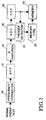
- Fig. 1 shows a schematic block diagram of a conventional signal analyzer for analyzing the frequency domain of a signal under test.
- a frequency converter 10 which has a mixer and a local oscillator etc. converts a signal under test into an IF (Intermediate Frequency) signal.
- a band pass filter (BPF) 12 makes the IF signal have a suitable bandwidth.
- An IF amplifier 14 amplifies the output signal of the BPF 12 and an analog to digital converter (ADC) 16 converts it into a digital signal.
- a digital signal processor (DSP) 18 transforms the output signal of the ADC 16 into the frequency domain data by the Fast Fourier Transformation (FFT) process.
- a memory 20 sequentially stores the frequency domain data.
- FFT Fast Fourier Transformation
- a trigger detector 21 detects whether the frequency domain data satisfies a predetermined trigger condition or not. That is, the trigger detector 21 compares the data set as the trigger condition with the frequency domain data of the signal under test and generates a trigger signal if the condition is satisfied.
- the data of the trigger condition is decided like that an operator specifies a zone in a measuring region on a display screen (not shown) as the trigger condition, on which the horizontal and vertical axes indicate frequency and amplitude, respectively.
- a memory controller 23 controls the storage operation of the memory 20 according to the trigger signal generation. In more detail, it can control the time up to the stop of the storage operation of the memory 20 after the time of the trigger generation. If the memory 20 stops the storage operation soon from the trigger signal generation, it stores the data up to the time of the trigger signal generation. This operation provides a pretrigger function. On the other hand, if the memory 20 stops the storage operation after continuing the storage for some period from the trigger signal generation, it stores the data mainly after the time of the trigger signal generation. This provides a post-trigger function.
- the data stored in the memory 20 in such a way as described above are displayed on a suitable display like a cathode ray tube or a liquid crystal display etc. for the frequency domain analysis of the signal.
- the present invention provides a wide band analyzer as specified in claim 1.
- Preferred embodiments of the invention are described in the subclaims.
- the present invention provides a wide band signal analyzer suitable for analyzing the frequency domain of a signal under test at low cost with controlling the characteristics degradation.
- a signal conversion means converts a signal under test into an intermediate frequency signal.
- a narrow band signal processing means receives the intermediate frequency signal for producing a first digital signal representing a specific frequency band of the intermediate frequency signal.
- the narrow band signal processing means has a usual configuration similar to the conventional one and is used for measuring the narrow band side.
- a wide band signal processing means receives the intermediate frequency signal for producing a second digital signal representing a wider frequency band including said specific frequency band of the intermediate frequency signal.
- the optimum devices can be selected for both the narrow and wide signal processing means that provides an advantage from technical and economical viewpoints.
- a decelerating means decelerates the transfer rate of the second digital data so that the following devices are not required in the high speed operation.
- a selecting means selects the first digital signal or the output signal of the decelerating means.
- a processing means processes the output signal of the selecting means by some process such as the FFT process.
- a memory means stores the processed output of the processing means. The data in the memory means is used for displaying the measurement result or another analysis.
- a trigger detecting means detects whether the output signal of the processing means satisfies a predetermined trigger condition.
- a control means controls the decelerating means according to the output signal of the trigger detecting means if the measurement frequency band of the signal under test is over said specific frequency band.
- the output signal of the processing means is derived from the narrow band signal processing means for detecting whether it satisfies the predetermined trigger condition. Therefore, the trigger function concerning the wide bandwidth is realized by a slight modification relative to the conventional narrow one.
- Fig. 2 shows a schematic block diagram of one preferred embodiment according to the present invention.
- the elements corresponding to those of Fig. 1 have the same reference symbols, respectively.
- a frequency converter 10 converts a signal under test into a suitable IF (Intermediate Frequency) signal.
- the frequency converter 10 may have a mixer and a local oscillator etc. as usual.
- the frequency converter 10 provides the IF signal to both band pass filter (BPF) 12 and wide band pass filter 22.
- BPF 12 could be a filter similar to the conventional one as shown in Fig. 1, and has a narrow band pass width, such as 5MHz, then can be the input of a signal pass for a narrow band side.
- the wide BPF 22 has a wider bandwidth than that of the BPF 12 and can be the input of a signal pass for a wide band side.
- the output of the BPF 12 is connected to an IF amplifier 14 and the output of the IF amplifier 14 is connected to an ADC (Analog To Digital Converter) 16 as usual.
- This signal pass of the narrow band side, having the BPF 12, the IF amplifier 14 and the ADC 16, is the same as the conventional one as shown in Fig. 1.
- the wide BPF 22 has a wider bandwidth, such as 30MHz. Therefore, the output signal of the wide BPF 22 has wider bandwidth and the maximum frequency is higher than that of the output signal of the BPF 12.
- a wide band IF amplifier 24 appropriately amplifies the output signal of the wide BPF 22 and a fast ADC 26 converts it into a digital signal.
- the sampling theorem as is well known to the man skilled in the art tells that the sampling frequency in the analog to digital conversion needs at least two times of the maximum frequency of the analog input signal. Then the sampling frequency of the fast ADC 26 should have two or over times of the maximum frequency of the output signal of the wide band IF amplifier 24. This leads it to that the transfer rate of the output data of the fast ADC 26 is higher than that of the ADC 16 in the narrow band side.
- a FIFO (First In First Out) memory 28 stores the output data of the fast ADC 26 sequentially.
- the FIFO, or first in first out memory 28 provides sequential storage and read out of the data. If the FIFO memory 28 becomes full before the storage operation stops, it stores the latest data with deleting the oldest data.
- the FIFO memory 28 also works as a means for reducing the data transfer rate and makes it possible that the speed of reading the data is slower than that of the data storage. This allows that the data transfer rate of the output data of the FIFO memory 28 meets that of the ADC 16.
- a multiplexer (MPX) 30 receives the output signals of both the ADC 16 and the FIFO memory 28 and works as a means for selecting one of them.
- a DSP (Digital Signal Processor) 18 receives the output signal of the multiplexer 30 and conducts a necessary process, such as FFT, similar to the conventional one. If the DSP 18 conducts the FFT process, it produces the frequency domain data corresponding to the output data of the multiplexer 30.
- a memory 20 stores the output data of the DSP 18. The data stored in the memory 20 could be used for displaying the measurement result on a display (not shown), such as CRT, or for another analysis.
- the DSP 18 provides the output data to a trigger detector 32 as well as the memory 20.
- the trigger detector 32 compares the frequency domain data from the DSP 18 with a preset trigger condition data and generates a trigger signal if the trigger condition is satisfied.
- the memory controller 34 receives the trigger signal and controls the memory 20 and/or the FIFO memory 28 according to the trigger signal.
- the analyzer In use of the analyzer, the operator selects the narrow band or wide band for measurement. If the operator selects a relatively narrow bandwidth for analysis, the memory controller 34 controls the storage operation of the memory 20 for the trigger function, and the operation is the same as that of the conventional analyzer shown in Fig. 1.
- the analyzer realizes the pre-trigger and post-trigger functions as described above. In this case, the FIFO memory 28 is not used.
- the memory controller 34 controls the storage operation of the FIFO memory 28, containing the digital data produced by the wide band signal processor.
- the memory controller 34 controls the data remaining in the FIFO memory according to the trigger function, such as pre-trigger or post-trigger function, with reference to the trigger signal generated by the trigger detector 32 based on the frequency domain data acquired by the narrow band signal processor.
- the control of the FIFO memory 28 realizes an effective event trigger operation in the wide band signal process.
- the memory 20 may store the data derived from the output signal of the ADC 16 via the DSP 18.
- the frequency domain data output from the DSP 18 for detecting a trigger event are such data as produced by a narrow band processing means which has the BPF 12, the IF amplifier 14 and the ADC 16.
- the trigger detector 32 detects the trigger by using the frequency domain data acquired in the narrow band signal processing, while the memory controller 34 controls the data produced in the wide band signal process and stored in the FIFO memory 28. Therefore, it can realize the trigger function useful enough with slight modification relative to the conventional one and with the minimum cost up while it also realizes the wide band signal processing.
- it can also easily realize the pre-trigger and post-trigger functions as usual event trigger functions by controlling the storage operation of the FIFO memory 28.
- the multiplexer 30 selects the data read out from the FIFO memory 28 to provide them to the DSP 18.
- the DSP 18 transforms the data by the FFT process to produce the frequency domain data of the wide band signal process.
- the memory 20 stores the frequency domain data of the wide band signal process, which are used for displaying the measurement result on the CRT etc. or for another analysis.
- the data previously stored in the memory 20 from the narrow band processing means may be transferred to another memory, such as a magnetic disk, if the memory 20 has insufficient capacity.
- the trigger function may not be used.
- the data is continuously acquired from one of the narrow and wide band signal processing paths and displayed.
- the data derived from the wide band signal processing path sometimes requires suspend time of the data acquisition because of the decelerated data output.
- a wide band signal analyzer can use the construction similar to the conventional one. Therefore it does not cause the spurious characteristics worse or noise because of the wider band.
- Both the signal passes of the narrow and wide band sides can be constructed from the optimum devices of filters, amplifiers and ADCs, respectively, according to the measurement band so that it is favorable from technical and economical viewpoints. Because it has a means for decelerating the data transfer rate of the output data of the fast analog to digital converter, the operation speed of the DSP 18 or memory 20 can be slow, which reduces the cost increase at the minimum. It can easily realize an event trigger function in the wide band signal process with slight modification relative to the conventional one and with the minimum cost increase. It will also be apparent for the man skilled in the art that there are additional embodiments which are not described above but which are clearly within the scope and principle of the present invention, as defined in the claims.
Landscapes
- Physics & Mathematics (AREA)
- Mathematical Physics (AREA)
- General Physics & Mathematics (AREA)
- Monitoring And Testing Of Transmission In General (AREA)
- Measurement Of Resistance Or Impedance (AREA)
- Measurement Of Mechanical Vibrations Or Ultrasonic Waves (AREA)
- Measuring Frequencies, Analyzing Spectra (AREA)
Abstract
Description
Claims (13)
- A wide band signal analyzer comprising:a frequency converter (10) for converting a signal under test to an intermediate frequency signal,a narrow band signal processor (12, 14, 16) for receiving the intermediate frequency signal and producing a first digital signal representing a first frequency band of the intermediate frequency signal,a wide band signal processor (22, 24, 26) for receiving the intermediate frequency signal and producing a second digital signal representing a second frequency band of the intermediate frequency signal,a transfer rate decelerator (28) for decelerating the transfer rate of the second digital signal,a digital processor (18, 30) for processing selectively the first digital signal or the output signal of the transfer rate decelerator (28), anda memory (20) for storing the processed output of the digital processor (18, 30).
- A wide band signal analyzer according to claim 1, further comprising:a trigger detector (32) for detecting whether the output signal of the digital processor (18, 30) satisfies a predetermined trigger condition, anda controller (34) for controlling the transfer rate decelerator (28) according to the output signal of the trigger detector (32) if the measurement frequency band of the signal under test is wider than the first frequency band.
- A wide band signal analyzer according to claim 1 or 2, wherein the second frequency band includes the first frequency band, and the output signal of the digital processor (18, 30) is derived from the narrow band signal processor (12, 14, 16) for detecting whether it satisfies the predetermined trigger condition.
- A wide band signal analyzer according to any one of claims 1 to 3, wherein the transfer rate decelerator (28) temporarily stores the second digital signal and the controller (34) is operable to adjust the interval between the time that occurrence of the trigger condition is detected and the time at which storing of the second digital signal by the transfer rate decelerator (28) terminates.
- A wide band signal analyzer according to claim 1, wherein the digital processor (18, 30) selects to process the first digital signal if the measurement frequency band of the signal under test is within said first frequency band and selects to process the output signal of the transfer rate decelerator (28) if the measurement frequency band of the signal under test is wider than the first frequency band.
- A wide band signal analyzer according to any one of claims 1 to 5, wherein the narrow band signal processor (12, 14, 16) includes a band pass filter (12) for passing the first frequency band of the intermediate frequency signal, and an analog to digital converter (16) for converting the output signal of the band pass filter (12) to produce the first digital signal.
- A wide band signal analyzer according to claim 6, wherein the narrow band signal processor (12, 14, 16) includes an intermediate frequency amplifier (14) between the output of the band pass filter (12) and the input of the analog to digital converter (16).
- A wide band signal analyzer according to any one of claims 1 to 7, wherein the wide band signal processor (22, 24, 26) includes a wide band pass filter (22) for passing the second frequency band of the intermediate frequency signal, and a fast analog to digital converter (26) for converting the output signal of the wide band pass filter (22) to produce the second digital signal.
- A wide band signal analyzer according to claim 8, wherein the wide band signal processor (22, 24, 26) includes a wide band intermediate frequency amplifier (24) between the output of the wide band pass filter (22) and the input of the fast analog to digital converter (26).
- A wide band signal analyzer according to any one of claims 1 to 9, wherein the transfer rate decelerator (28) includes a FIFO memory (28) for sequentially storing the output signal of narrow band signal processor (12, 14, 16), of which the read out rate is slower than the storage rate.
- A wide band signal analyzer according to any one of claims 1 to 10, wherein the digital processor (18, 30) performs an FFT process for producing the frequency domain data of the selected signal.
- A wide band signal analyzer according to any one of claims 1 to 11, wherein the transfer rate decelerator (28) temporarily stores the second digital signal and if the transfer rate decelerator (28) becomes full before the storage operation terminates, it stores the most recent data and deletes the oldest data.
- A wide band signal analyzer according to any one of claims 1 to 12, wherein the digital processor (18, 30) includes a selector (30) for selecting the first digital signal or the output signal of the transfer rate decelerator (28) and a digital signal processor (18) for processing the signal selected by the selector (30).
Applications Claiming Priority (4)
| Application Number | Priority Date | Filing Date | Title |
|---|---|---|---|
| JP22625498 | 1998-08-10 | ||
| JP22625498 | 1998-08-10 | ||
| JP23683898 | 1998-08-24 | ||
| JP23683898 | 1998-08-24 |
Publications (3)
| Publication Number | Publication Date |
|---|---|
| EP0981054A2 true EP0981054A2 (en) | 2000-02-23 |
| EP0981054A3 EP0981054A3 (en) | 2001-08-22 |
| EP0981054B1 EP0981054B1 (en) | 2006-08-30 |
Family
ID=26527084
Family Applications (1)
| Application Number | Title | Priority Date | Filing Date |
|---|---|---|---|
| EP99115116A Expired - Lifetime EP0981054B1 (en) | 1998-08-10 | 1999-08-10 | Wide band signal analyzer |
Country Status (3)
| Country | Link |
|---|---|
| US (1) | US6356067B1 (en) |
| EP (1) | EP0981054B1 (en) |
| DE (1) | DE69932981T2 (en) |
Cited By (4)
| Publication number | Priority date | Publication date | Assignee | Title |
|---|---|---|---|---|
| EP1885080A1 (en) | 2006-08-02 | 2008-02-06 | Innowireless Co., Ltd. | Apparatus and method for synchronizing signal analyzer |
| CN103837725A (en) * | 2012-11-20 | 2014-06-04 | 特克特朗尼克公司 | Combinatorial mask triggering in time or frequency domain |
| CN110361999A (en) * | 2019-06-13 | 2019-10-22 | 南京理工大学 | Active optics micro-displacement sensor signal processing system and method based on DSP |
| EP3671232A1 (en) * | 2018-12-19 | 2020-06-24 | Thales | Device for analysing a signal and associated method |
Families Citing this family (14)
| Publication number | Priority date | Publication date | Assignee | Title |
|---|---|---|---|---|
| US6507624B1 (en) * | 1999-04-21 | 2003-01-14 | Tektronix, Inc. | Bandpass sampling architecture for wide-frequency band signal analysis |
| JP3962785B2 (en) * | 2003-07-02 | 2007-08-22 | テクトロニクス・インターナショナル・セールス・ゲーエムベーハー | Signal analyzer and frequency domain data generation method |
| US7519330B2 (en) * | 2004-03-08 | 2009-04-14 | Tektronix, Inc. | Simultaneous ACLR measurement |
| US7352827B2 (en) * | 2004-03-18 | 2008-04-01 | Tektronix, Inc. | Multichannel simultaneous real time spectrum analysis with offset frequency trigger |
| US7292985B2 (en) * | 2004-12-02 | 2007-11-06 | Janus Development Group | Device and method for reducing stuttering |
| JP2008010909A (en) * | 2006-06-27 | 2008-01-17 | Niigata Seimitsu Kk | Automatic gain control circuit |
| JP5085105B2 (en) * | 2006-11-24 | 2012-11-28 | テクトロニクス・インターナショナル・セールス・ゲーエムベーハー | Signal analyzer |
| US8514919B2 (en) * | 2009-08-26 | 2013-08-20 | Bae Systems National Security Solutions Inc. | Synthetic instrument unit |
| CN102412916B (en) * | 2011-11-17 | 2015-11-11 | 大唐移动通信设备有限公司 | A kind of VSA |
| US9008235B2 (en) | 2013-02-19 | 2015-04-14 | Broadcom Corporation | Receiver with reduced wake-up time |
| WO2016201453A1 (en) | 2015-06-12 | 2016-12-15 | Bird Technologies Group, Inc. | Channel-selective rf power sensor |
| US10608916B2 (en) * | 2017-03-23 | 2020-03-31 | Rohde & Schwarz Gmbh & Co. Kg | Measuring device and method for dynamically selecting a channel bandwidth |
| US10365301B2 (en) * | 2017-05-01 | 2019-07-30 | Rohde & Schwarz Gmbh & Co. Kg | Oscilloscope acquisition system |
| EP3486678B1 (en) * | 2017-11-17 | 2023-08-30 | Rohde & Schwarz GmbH & Co. KG | Multi-signal instantaneous frequency measurement system |
Family Cites Families (31)
| Publication number | Priority date | Publication date | Assignee | Title |
|---|---|---|---|---|
| US3984769A (en) * | 1956-07-26 | 1976-10-05 | American Standard, Inc. | Mixed-base intercept receiver |
| US3631339A (en) * | 1970-08-13 | 1971-12-28 | Nasa | Method and apparatus for high-resolution spectral analysis |
| US3743783A (en) * | 1971-02-22 | 1973-07-03 | J Agnello | Apparatus for simultaneously recording speech spectra and physiological data |
| US3831088A (en) * | 1973-08-01 | 1974-08-20 | Us Navy | Pulsed signal phase lock spectral purity measuring apparatus |
| US3876946A (en) * | 1973-10-31 | 1975-04-08 | Singer Co | Radio frequency digital fourier analyzer |
| US4181822A (en) * | 1978-03-07 | 1980-01-01 | Bell & Howell Company | Bandsplitter systems |
| US4257119A (en) * | 1978-12-29 | 1981-03-17 | Wescom Switching, Inc. | PCM switching system for wide and narrow band signals |
| US4535286A (en) * | 1979-11-02 | 1985-08-13 | Raytheon Company | Radio frequency receiver |
| NL8203599A (en) * | 1982-09-17 | 1984-04-16 | Philips Nv | MAIN END AND RECEIVER FOR A SIGNAL DISTRIBUTION SYSTEM. |
| GB2134269B (en) * | 1983-01-22 | 1986-07-02 | Marconi Instruments Ltd | Frequency counting |
| JPS59157575A (en) * | 1983-02-27 | 1984-09-06 | Anritsu Corp | Spectrum analyzer |
| DE3330233A1 (en) * | 1983-08-22 | 1985-03-21 | Deutsche Forschungs- und Versuchsanstalt für Luft- und Raumfahrt e.V., 5000 Köln | METHOD AND DEVICE FOR ADJUSTING THE PID BEHAVIOR OF REGULATOR COMPENSATION NETWORKS, ESPECIALLY IN HYDROPULSE MACHINES |
| US4839582A (en) * | 1987-07-01 | 1989-06-13 | Anritsu Corporation | Signal analyzer apparatus with automatic frequency measuring function |
| US4975633A (en) | 1988-04-11 | 1990-12-04 | Anritsu Corporation | Spectrum analyzer having means for displaying spectrum data together with power value thereof |
| CA1312656C (en) * | 1989-08-24 | 1993-01-12 | Steven Messenger | Wireless communications systems |
| US4994740A (en) * | 1989-09-25 | 1991-02-19 | The United States Of America As Represented By The Secretary Of The Army | High resolution, wide band Chirp-Z signal analyzer |
| JPH03117076A (en) * | 1989-09-28 | 1991-05-17 | Matsushita Electric Ind Co Ltd | Sub-sample signal processor |
| JP2891497B2 (en) | 1990-01-25 | 1999-05-17 | アンリツ株式会社 | Spectrum analyzer |
| US5061930A (en) * | 1990-06-12 | 1991-10-29 | Westinghouse Electric Corp. | Multi-mode missile seeker system |
| JP2591864B2 (en) * | 1991-01-30 | 1997-03-19 | 日本電気アイシーマイコンシステム株式会社 | Digital filter |
| JPH04302501A (en) * | 1991-03-29 | 1992-10-26 | Anritsu Corp | Signal selection device |
| DE69227824T2 (en) * | 1991-09-02 | 1999-06-10 | Advantest Corp., Tokio/Tokyo | SPECTRUM ANALYZER |
| US5706385A (en) * | 1993-12-08 | 1998-01-06 | Hitachi, Ltd. | Rotary head type magnetic recording and reproducing apparatus |
| US5424631A (en) * | 1994-01-03 | 1995-06-13 | Itt Corporation | Hybrid instantaneous frequency measurement compressive receiver apparatus and method |
| JP2751840B2 (en) * | 1994-09-12 | 1998-05-18 | 日本電気株式会社 | Signal detection device |
| US5530373A (en) | 1995-01-20 | 1996-06-25 | Fluke Corporation | Method and apparatus for determining and selectively displaying valid measurement information |
| US5761190A (en) * | 1995-02-20 | 1998-06-02 | Pioneer Electronic Corporation | OFDM broadcast wave receiver |
| US5598288A (en) * | 1995-07-31 | 1997-01-28 | Northrop Grumman Corporation | RF fiber optic transmission utilizing dither |
| US5731699A (en) | 1996-02-12 | 1998-03-24 | Gte Laboratories Incorporated | Apparatus and method for simultaneous measuring of narrow and wideband RF transmission statistics |
| US5982819A (en) * | 1996-09-23 | 1999-11-09 | Motorola, Inc. | Modulation format adaptive messaging receiver and method thereof |
| GB2326546B (en) * | 1997-06-20 | 2001-01-03 | Nokia Mobile Phones Ltd | Gain control |
-
1999
- 1999-08-05 US US09/370,785 patent/US6356067B1/en not_active Expired - Fee Related
- 1999-08-10 DE DE69932981T patent/DE69932981T2/en not_active Expired - Lifetime
- 1999-08-10 EP EP99115116A patent/EP0981054B1/en not_active Expired - Lifetime
Cited By (7)
| Publication number | Priority date | Publication date | Assignee | Title |
|---|---|---|---|---|
| EP1885080A1 (en) | 2006-08-02 | 2008-02-06 | Innowireless Co., Ltd. | Apparatus and method for synchronizing signal analyzer |
| CN103837725A (en) * | 2012-11-20 | 2014-06-04 | 特克特朗尼克公司 | Combinatorial mask triggering in time or frequency domain |
| CN103837725B (en) * | 2012-11-20 | 2018-09-07 | 特克特朗尼克公司 | Test and sensing device and the method triggered for the template on test and sensing device |
| EP3671232A1 (en) * | 2018-12-19 | 2020-06-24 | Thales | Device for analysing a signal and associated method |
| FR3090886A1 (en) * | 2018-12-19 | 2020-06-26 | Thales | Signal analysis device and associated method |
| AU2019283797B2 (en) * | 2018-12-19 | 2025-01-16 | Thales | Device for analyzing a signal and associated method |
| CN110361999A (en) * | 2019-06-13 | 2019-10-22 | 南京理工大学 | Active optics micro-displacement sensor signal processing system and method based on DSP |
Also Published As
| Publication number | Publication date |
|---|---|
| EP0981054A3 (en) | 2001-08-22 |
| DE69932981D1 (en) | 2006-10-12 |
| EP0981054B1 (en) | 2006-08-30 |
| US6356067B1 (en) | 2002-03-12 |
| DE69932981T2 (en) | 2007-03-15 |
Similar Documents
| Publication | Publication Date | Title |
|---|---|---|
| EP0981054B1 (en) | Wide band signal analyzer | |
| US6198427B1 (en) | Doppler complex FFT police radar with direction sensing capability | |
| JP4762382B2 (en) | Spectrum analyzer | |
| JP2002506525A5 (en) | ||
| JP3431544B2 (en) | Wideband signal analyzer | |
| JPH0769365B2 (en) | Spectrum analyzer | |
| CN110221261B (en) | Radar waveform generation module test analysis method and device | |
| CN108303587A (en) | Improve the spectrum analyzer that bottom is made an uproar | |
| KR19990045594A (en) | Speed measuring device | |
| US6166673A (en) | Data acquisition system and method with a selectable sampling rate | |
| JPH11271183A (en) | Vibration data-collecting device | |
| EP2073027A1 (en) | Methods and systems for determining a received signal frequency | |
| EP0019398A1 (en) | Monitoring apparatus for rotating machinery | |
| JPH09178547A (en) | Multipoint simultaneous measurement system | |
| JP2985579B2 (en) | Signal processing device for ultrasonic flaw detector | |
| JP2662406B2 (en) | Data collection device for partial discharge measurement device | |
| JP3672834B2 (en) | Receiver | |
| SU558224A1 (en) | Device for automatically measuring the amplitudes of a variable signal | |
| JP2574636Y2 (en) | Waveform analyzer | |
| US8355881B2 (en) | Device and process for machine diagnostics by means of vibration measurement | |
| JP2970816B2 (en) | Ultrasonic measuring device | |
| JPH1151990A (en) | Waveform analyzing device | |
| JPH0772190A (en) | Fast Fourier transform analyzer | |
| JPH0763797A (en) | Fast Fourier transform analyzer | |
| JPH0783971A (en) | Fast Fourier transform analyzer |
Legal Events
| Date | Code | Title | Description |
|---|---|---|---|
| PUAI | Public reference made under article 153(3) epc to a published international application that has entered the european phase |
Free format text: ORIGINAL CODE: 0009012 |
|
| AK | Designated contracting states |
Kind code of ref document: A2 Designated state(s): AT BE CH CY DE DK ES FI FR GB GR IE IT LI LU MC NL PT SE |
|
| AX | Request for extension of the european patent |
Free format text: AL;LT;LV;MK;RO;SI |
|
| 17P | Request for examination filed |
Effective date: 20000720 |
|
| PUAL | Search report despatched |
Free format text: ORIGINAL CODE: 0009013 |
|
| AK | Designated contracting states |
Kind code of ref document: A3 Designated state(s): AT BE CH CY DE DK ES FI FR GB GR IE IT LI LU MC NL PT SE |
|
| AX | Request for extension of the european patent |
Free format text: AL;LT;LV;MK;RO;SI |
|
| AKX | Designation fees paid |
Free format text: DE FR |
|
| RAP1 | Party data changed (applicant data changed or rights of an application transferred) |
Owner name: TEKTRONIX JAPAN, LTD. |
|
| 17Q | First examination report despatched |
Effective date: 20031006 |
|
| GRAP | Despatch of communication of intention to grant a patent |
Free format text: ORIGINAL CODE: EPIDOSNIGR1 |
|
| GRAS | Grant fee paid |
Free format text: ORIGINAL CODE: EPIDOSNIGR3 |
|
| GRAA | (expected) grant |
Free format text: ORIGINAL CODE: 0009210 |
|
| AK | Designated contracting states |
Kind code of ref document: B1 Designated state(s): DE FR |
|
| REF | Corresponds to: |
Ref document number: 69932981 Country of ref document: DE Date of ref document: 20061012 Kind code of ref document: P |
|
| ET | Fr: translation filed | ||
| PLBE | No opposition filed within time limit |
Free format text: ORIGINAL CODE: 0009261 |
|
| STAA | Information on the status of an ep patent application or granted ep patent |
Free format text: STATUS: NO OPPOSITION FILED WITHIN TIME LIMIT |
|
| 26N | No opposition filed |
Effective date: 20070531 |
|
| PGFP | Annual fee paid to national office [announced via postgrant information from national office to epo] |
Ref country code: FR Payment date: 20120906 Year of fee payment: 14 Ref country code: DE Payment date: 20120822 Year of fee payment: 14 |
|
| PG25 | Lapsed in a contracting state [announced via postgrant information from national office to epo] |
Ref country code: DE Free format text: LAPSE BECAUSE OF NON-PAYMENT OF DUE FEES Effective date: 20140301 |
|
| REG | Reference to a national code |
Ref country code: DE Ref legal event code: R119 Ref document number: 69932981 Country of ref document: DE Effective date: 20140301 |
|
| REG | Reference to a national code |
Ref country code: FR Ref legal event code: ST Effective date: 20140430 |
|
| PG25 | Lapsed in a contracting state [announced via postgrant information from national office to epo] |
Ref country code: FR Free format text: LAPSE BECAUSE OF NON-PAYMENT OF DUE FEES Effective date: 20130902 |