EP1876704A2 - Regulation of an amplification apparatus - Google Patents
Regulation of an amplification apparatus Download PDFInfo
- Publication number
- EP1876704A2 EP1876704A2 EP07111332A EP07111332A EP1876704A2 EP 1876704 A2 EP1876704 A2 EP 1876704A2 EP 07111332 A EP07111332 A EP 07111332A EP 07111332 A EP07111332 A EP 07111332A EP 1876704 A2 EP1876704 A2 EP 1876704A2
- Authority
- EP
- European Patent Office
- Prior art keywords
- signal
- amplifier
- supply voltage
- amplification apparatus
- stage
- Prior art date
- Legal status (The legal status is an assumption and is not a legal conclusion. Google has not performed a legal analysis and makes no representation as to the accuracy of the status listed.)
- Granted
Links
- 230000003321 amplification Effects 0.000 title claims abstract description 50
- 238000003199 nucleic acid amplification method Methods 0.000 title claims abstract description 50
- 230000005540 biological transmission Effects 0.000 claims description 35
- 238000000034 method Methods 0.000 claims description 14
- 230000001105 regulatory effect Effects 0.000 claims description 8
- 238000005516 engineering process Methods 0.000 description 5
- 239000003990 capacitor Substances 0.000 description 4
- 238000001914 filtration Methods 0.000 description 4
- 239000004065 semiconductor Substances 0.000 description 4
- 238000004891 communication Methods 0.000 description 2
- 230000001419 dependent effect Effects 0.000 description 2
- 238000013459 approach Methods 0.000 description 1
- 230000000295 complement effect Effects 0.000 description 1
- 229910044991 metal oxide Inorganic materials 0.000 description 1
- 150000004706 metal oxides Chemical class 0.000 description 1
- 238000010295 mobile communication Methods 0.000 description 1
Images


Classifications
-
- H—ELECTRICITY
- H03—ELECTRONIC CIRCUITRY
- H03F—AMPLIFIERS
- H03F1/00—Details of amplifiers with only discharge tubes, only semiconductor devices or only unspecified devices as amplifying elements
- H03F1/02—Modifications of amplifiers to raise the efficiency, e.g. gliding Class A stages, use of an auxiliary oscillation
- H03F1/0205—Modifications of amplifiers to raise the efficiency, e.g. gliding Class A stages, use of an auxiliary oscillation in transistor amplifiers
- H03F1/0261—Modifications of amplifiers to raise the efficiency, e.g. gliding Class A stages, use of an auxiliary oscillation in transistor amplifiers with control of the polarisation voltage or current, e.g. gliding Class A
-
- H—ELECTRICITY
- H03—ELECTRONIC CIRCUITRY
- H03F—AMPLIFIERS
- H03F1/00—Details of amplifiers with only discharge tubes, only semiconductor devices or only unspecified devices as amplifying elements
- H03F1/02—Modifications of amplifiers to raise the efficiency, e.g. gliding Class A stages, use of an auxiliary oscillation
- H03F1/0205—Modifications of amplifiers to raise the efficiency, e.g. gliding Class A stages, use of an auxiliary oscillation in transistor amplifiers
-
- H—ELECTRICITY
- H03—ELECTRONIC CIRCUITRY
- H03F—AMPLIFIERS
- H03F3/00—Amplifiers with only discharge tubes or only semiconductor devices as amplifying elements
- H03F3/20—Power amplifiers, e.g. Class B amplifiers, Class C amplifiers
- H03F3/24—Power amplifiers, e.g. Class B amplifiers, Class C amplifiers of transmitter output stages
-
- H—ELECTRICITY
- H03—ELECTRONIC CIRCUITRY
- H03F—AMPLIFIERS
- H03F2200/00—Indexing scheme relating to amplifiers
- H03F2200/108—A coil being added in the drain circuit of a FET amplifier stage, e.g. for noise reducing purposes
-
- H—ELECTRICITY
- H03—ELECTRONIC CIRCUITRY
- H03F—AMPLIFIERS
- H03F2200/00—Indexing scheme relating to amplifiers
- H03F2200/18—Indexing scheme relating to amplifiers the bias of the gate of a FET being controlled by a control signal
-
- H—ELECTRICITY
- H03—ELECTRONIC CIRCUITRY
- H03F—AMPLIFIERS
- H03F2200/00—Indexing scheme relating to amplifiers
- H03F2200/181—A coil being added in the gate circuit of a FET amplifier stage, e.g. for noise reducing purposes
-
- H—ELECTRICITY
- H03—ELECTRONIC CIRCUITRY
- H03F—AMPLIFIERS
- H03F2200/00—Indexing scheme relating to amplifiers
- H03F2200/318—A matching circuit being used as coupling element between two amplifying stages
Definitions
- the output amplifier may be subject to strict constraints on linearity and efficiency. If the transmitter is using an amplitude modulation such as 8-PSK modulation used in GSM EDGE (Enhanced Data GSM Environment), the output amplifier has to be arranged so that the output signal is linear in relation to the input signal to avoid a distortion of the output signal.
- amplitude modulation such as 8-PSK modulation used in GSM EDGE (Enhanced Data GSM Environment)
- GSM EDGE Enhanced Data GSM Environment
- the efficiency of the output amplifier is defined by the ratio of an outgoing power level at an output of the output amplifier to the power input into the output amplifier. The lower that ratio the more efficient the input power is brought onto the outgoing signal. This is advantageous if the transmitter is part of a mobile terminal having only limited power resources.
- the transmitter illustrated in Figure 1 includes a transformer 101 that produces a first amplitude information signal and a phase information signal.
- the transformer 101 produces these signals according to input signals that in various embodiments might be delivered as Cartesian information such as quadrature modulated information or inphase and quadrature signals.
- the ingoing signals may be provided by a baseband unit that includes a microcontroller, a DSP or by any other suitable processing element.
- the input signals are containing information i.e. data to be transmitted by the transmitter via a transmission channel such as a wireless or wireline channel.
- the amplification apparatus includes a supply voltage circuitry 207 that is coupled to the pre-amplifier stage 204 to provide a supply voltage thereto.
- the supply voltage is variable and is regulated by the supply voltage circuitry 207.
- a collector of the second npn-transistor 304 is connected to a local supply voltage node 308.
- a collector of the third npn-transistor 305 is connected via a first inductor 309 to the local supply voltage node 308.
- the first npn-transistor 303 and the differential pair of the second npn-transistor 304 and the third npn-transistor 305 thus form a differential amplifier with variable gain.
- the gain is set by a gain setting voltage disposed at the first gain setting voltage input 306 and the second gain setting voltage input 307.
- a radio frequency signal to be amplified is received at the signal input 301.
- a first amplified signal being the radio frequency signal amplified by a gain determined by the gain setting voltage is disposed at the collector of the third npn-transistor 305.
- the embodiment is implemented in a bipolar semiconductor technology, while the regulator is realized as the PMOS-transistor 319.
- the amplification apparatus is realized in a CMOS (Complementary Metal-Oxide Semiconductor) technology. Other semiconductor technology may be suitable as well.
- the PMOS-transistor 319 may be replaced by a bipolar transistor, by an NMOS-transistor or a regulation circuitry.
- the PMOS-transistor 319 is replaced by a switched regulator.
- the amplitude information may be imprinted on the outgoing signal by means of the gain setting voltage or by means of a supply voltage control signal received by the supply voltage control input 318. The two of the gain setting voltage or the supply voltage control signal may also be used together or separately for a ramping process or an adjustment of the power level of the outgoing signal during transmission.
- An emitter of the first pnp-transistor 405 is connected via a second resistor 406 to a second constant supply voltage input 407.
- the base of the first pnp-transistor 405 is connected to a base of a second pnp-transistor 408.
- An emitter of the second pnp-transistor 408 is connected via a third resistor 409 to the second constant supply voltage input 407.
- a collector of the second pnp-transistor 408 is connected to a collector of the seventh npn-transistor 404.
Landscapes
- Engineering & Computer Science (AREA)
- Power Engineering (AREA)
- Amplifiers (AREA)
- Control Of Electrical Variables (AREA)
Abstract
Description
- Embodiments of the present invention relate to an amplification apparatus, and more particular to a transmitter having an amplification apparatus, and a method for regulation of the amplification apparatus.
- In any electronic communication system a transmitter includes an output amplifier, i.e. an amplification apparatus that boosts the power of a transmission signal to a level sufficient to allow for a reception of the transmission signal by a receiver. Particularly in a wireless communication system, such as defined by the GSM (Global System for Mobile Communication) standard or defined by UMTS (Universal Mobile Telecommunication Standard), the power level of a mobile unit has to be adjusted according to rules given by a base station.
- In addition the output amplifier may be subject to strict constraints on linearity and efficiency. If the transmitter is using an amplitude modulation such as 8-PSK modulation used in GSM EDGE (Enhanced Data GSM Environment), the output amplifier has to be arranged so that the output signal is linear in relation to the input signal to avoid a distortion of the output signal.
- The efficiency of the output amplifier is defined by the ratio of an outgoing power level at an output of the output amplifier to the power input into the output amplifier. The lower that ratio the more efficient the input power is brought onto the outgoing signal. This is advantageous if the transmitter is part of a mobile terminal having only limited power resources.
- It is therefore a problem to provide an amplification apparatus, a transmitter apparatus and a method for regulating an amplification apparatus to allow for a mobile terminal having low power consumption.
- This problem is solved by an amplification apparatus according to claim 1, a transmission apparatus according to claim 15, and a method according to claim 23.
- Further embodiments of the invention and more detailed arrangements of the invention are shown in the dependent claims.
- Embodiments of the invention will be explained in detail in the following text with reference to the accompanying drawings, in which:
- Figure 1 illustrates an embodiment of a transmitter having an amplification apparatus;
- Figure 2 illustrates an embodiment of an amplification apparatus;
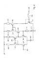
- Figure 3 illustrates an embodiment of an amplification apparatus; and
- Figure 4 illustrates an embodiment of a bias voltage circuitry.
- Figure 1 illustrates an embodiment of a transmitter having an amplification apparatus according to the present invention. It is understood that such amplification apparatus may be used in any application or circuitry to perform signal amplification.
- The transmitter illustrated in Figure 1 includes a
transformer 101 that produces a first amplitude information signal and a phase information signal. Thetransformer 101 produces these signals according to input signals that in various embodiments might be delivered as Cartesian information such as quadrature modulated information or inphase and quadrature signals. In various embodiments, the ingoing signals may be provided by a baseband unit that includes a microcontroller, a DSP or by any other suitable processing element. The input signals are containing information i.e. data to be transmitted by the transmitter via a transmission channel such as a wireless or wireline channel. - In the illustrated transmitter, the first amplitude information signal is fed into a first input of a
mixer 102. The phase information signal is fed into aphase modulator 103. Thephase modulator 103 modulates the phase information signal on a carrier frequency which is defined by the transmission channel. - The illustrated transmitter includes a
ramping control unit 104 that provides a power control signal that represents the ramping up or ramping down procedure for the transmitter. Theramping control unit 104 is connected to a second input of themixer 102. Themixer 102 mixes the first amplitude information signal and the power control signal to produce a second amplitude information signal. The mixing is performed by a digital multiplication of the first amplitude information signal and the power control signal. The second amplitude information signal is provided at an output of saidmixer 102. This signal includes the amplitude information of the signal to be transmitted and information about the ramping up and/or ramping down of the power level of the transmitter. - The output of
mixer 102 is connected to a digital-to-analog converter 105. The digital-to-analog converter 105 converts the second amplitude information signal from a digital form into an analog form of the second amplitude information signal. - An output of the digital-to-
analog converter 105 is connected to amodulator 106. An output of thephase modulator 103 is also connected to themodulator 106. Themodulator 106 modulates the amplitude information signal in its analog form on the phase information signal being shifted on the carrier frequency of the transmission system. Asignal output 107 of themodulator 106 provides an output signal that includes amplitude information, ramping information and/or phase information. In the illustrated transmitter themodulator 106 is an amplification apparatus according to an embodiment of the present invention. - The transmitter illustrated in Figure 1 includes digital signal processing in the transmission path. The ramping information is brought on the signal or combined with the signal to be transmitted in the digital domain of the transmitter. This is performed by means of the
mixer 102. Yet other suitable approaches may be used. - Figure 2 illustrates an embodiment of an amplification apparatus.
- The amplification apparatus includes a
signal input 201 for receiving a radio frequency signal to be transmitted. The radio frequency signal is fed by thesignal input 201 into a variablegain amplifier stage 202. The amplification apparatus includes asecond input 203 connected to thevariable gain amplifier 202. Thesecond input 203 is receiving a gain setting signal fed into the variablegain amplifier stage 202 so as to set a gain of the variablegain amplifier stage 202. An output of the variablegain amplifier stage 202 is connected to an input of apre-amplifier stage 204. An output of thepre-amplifier stage 204 is connected to an input of anoutput stage 205. An output of theoutput stage 205 is connected to asignal output 206. The series of the variablegain amplifier stage 202, thepre-amplifier stage 204, and theoutput stage 205 forms a transmission chain to boost the power of the radio frequency signal received at thesignal input 201 to a power level of an outgoing transmission signal disposed at thesignal output 206. In various embodiments, the transmission chain may include solely a pre-amplifier stage and an output stage. Other embodiments may include one or more additional amplifier stages to boost the signal. - The amplification apparatus includes a
supply voltage circuitry 207 that is coupled to thepre-amplifier stage 204 to provide a supply voltage thereto. The supply voltage is variable and is regulated by thesupply voltage circuitry 207. - In some embodiments the
supply voltage circuitry 207 is disconnected from theoutput stage 205 and theoutput stage 205 receives a constant supply voltage. This is particularly advantageous if most of the power of the transmission chain is realized in theoutput stage 205. The supply voltage circuitry can be regarded as a regulator regulating the output power level. A part of the power input in the amplification apparatus is dissipated in thesupply voltage circuitry 207. If the regulation of the output power level is performed in thepre-amplifier stage 204 and not in theoutput stage 205 the efficiency of the amplification apparatus is higher than compared to an embodiment usingsupply voltage circuitry 207 to regulate the supply voltage of theoutput stage 205. - Yet, in various other embodiments the supply voltage circuitry feeds a first supply voltage to the
pre-amplifier stage 204 and a second supply voltage to theoutput stage 205, and the first supply voltage and the second supply voltage differ in value. This is particularly advantageous if theoutput stage 205 is inserting a larger part of the power level into the transmission chain and regulating the output power level is also performed in the output stage, e.g. so to achieve a larger dynamic range. In other embodiments the first supply voltage and the second supply voltage are identical in value. - The
supply voltage circuitry 207 is connected to abias voltage circuitry 208 that is included in the amplification apparatus. Thebias voltage circuitry 208 is coupled to thepre-amplifier stage 204 and to theoutput stage 205. It feeds a respective bias voltage thereto. In various embodiments this bias voltage sets an operating point of thepre-amplifier stage 204 and/or theoutput stage 205. Thebias voltage circuitry 208 is coupled to thesupply voltage circuitry 207 and receives a supply voltage signal or a signal derived from or being in a relation to the supply voltage signal by thesupply voltage circuitry 207. In accordance with that supply voltage signal thebias voltage circuitry 208 produces the bias voltage fed to theoutput stage 205. In various embodiments the bias voltage fed into thepre-amplifier stage 204 remains unchanged. By this provision the transmission chain is linear. This is particularly advantageous in a transmission system using an amplitude modulation such as GSM-EDGE or UMTS. In other embodiments the bias voltage fed into thepre-amplifier stage 204 is changed as a function of the supply voltage. This might be performed in a transmission system like GSM-GMSK, WDCT or DECT where no linearity is required in the transmission chain. - The amplification apparatus further includes a supply
voltage control input 209 connected to thesupply voltage circuitry 207. In various embodiments a supply voltage control signal is fed into the supplyvoltage control input 209. In some embodiments the supply voltage control signal is provided by a baseband unit that includes a microcontroller, a DSP or any other suitable processing element. In some embodiments the supply voltage control signal is provided by a transformer and/or by a ramping control unit as shown e.g. in the transmitter of Figure 1. The supply voltage control signal may be used to control a ramping up and/or ramping down process of the amplification apparatus. In various embodiments the supply voltage control signal may also be used to imprint an amplitude modulation onto the signal processed by the amplification apparatus. The supply voltage control signal may correspond to the amplitude information signal shown in Figure 1. In some embodiments the supply voltage control signal may be used to regulate the power level of the outgoing signal during a transmission interval. - In various embodiments the gain setting signal fed into the variable
gain amplifier stage 202 is used to imprint an amplitude modulation onto the signal processed by the amplification apparatus. In different embodiments the gain setting signal is used to regulate the power level of the outgoing signal during a transmission interval. In various embodiments the gain setting signal corresponds to the amplitude information signal shown in Figure 1. - Figure 3 is a circuitry representation illustrating one embodiment of an amplification apparatus.
- The amplification apparatus includes a
signal input 301 connected to a first voltage node. The first voltage node is connected to a base of a first npn-transistor 303. An emitter of the first npn-transistor 303 is coupled via afirst resistor 302 to ground. A collector of the first npn-transistor 303 is connected to each of respective emitters of a differential pair of a second npn-transistor 304 and a third npn-transistor 305. A base of the second npn-transistor 304 is connected to a first gain settingvoltage input 306 and a base of the third npn-transistor 305 is connected to a second gain settingvoltage input 307. A collector of the second npn-transistor 304 is connected to a localsupply voltage node 308. A collector of the third npn-transistor 305 is connected via afirst inductor 309 to the localsupply voltage node 308. The first npn-transistor 303 and the differential pair of the second npn-transistor 304 and the third npn-transistor 305 thus form a differential amplifier with variable gain. The gain is set by a gain setting voltage disposed at the first gain settingvoltage input 306 and the second gain settingvoltage input 307. A radio frequency signal to be amplified is received at thesignal input 301. A first amplified signal being the radio frequency signal amplified by a gain determined by the gain setting voltage is disposed at the collector of the third npn-transistor 305. - The collector of the third npn-
transistor 305 is connected via afirst matching network 310 to a base of a fourth npn-transistor 311. An emitter of the fourth npn-transistor 311 is connected to ground. A collector of the fourth npn-transistor 311 is coupled via asecond inductor 312 to the localsupply voltage node 308. At the collector of the fourth npn-transistor 311 a second amplified signal derived from the first amplified signal is disposed. The fourth npn-transistor 311 being a grounded emitter amplifier represents a pre-amplifier stage, which amplifies the first amplified signal to produce the second amplified signal. The gain of the pre-amplifier is set by regulating the voltage disposed at the localsupply voltage node 308. - The
first matching network 310 may be a low pass filtering element comprising a series inductor and a shunt capacitor. In another embodiment thefirst matching network 310 is a high pass filtering element comprising a series capacitor and a shunt inductor. - The collector of the fourth npn-
transistor 311 is connected via asecond matching network 313 to a base of a fifth npn-transistor 314. An emitter of the fifth npn-transistor 314 is connected to ground. A collector of the fifth npn-transistor 314 is connected to asignal output 315. The fifth npn-transistor 314 being a grounded emitter amplifier represents an output stage, which amplifies the second amplified signal to produce an output signal. The collector of the fifth npn-transistor 314 is furthermore connected via athird inductor 316 to asupply voltage input 317. A global supply voltage disposed at thesupply voltage input 317 sets the gain of the fifth npn-transistor 314, i.e. the output stage. - The
second matching network 313 may be a low pass filtering element comprising a series inductor and a shunt capacitor. In an embodiment, thesecond matching network 313 is a high pass filtering element comprising a series capacitor and a shunt inductor. - The amplification apparatus includes a supply
voltage control input 318 connected to a gate of a PMOS-transistor 319. A drain of the PMOS-transistor 319 is connected to thesupply voltage input 317. A source of the PMOS-transistor 319 is connected to the localsupply voltage node 308. The PMOS-transistor 319 thus represents a linear regulator regulating the voltage disposed at the localsupply voltage node 308; said voltage being derived from the supply voltage in dependence of a supply voltage control signal received at the supplyvoltage control input 318. The voltage disposed at the localsupply voltage node 308 represents a supply voltage to the variable gain amplifier stage and the pre-amplifier stage. The PMOS-transistor 319 and the circuitry, which connects it to thesupply voltage input 317, the supplyvoltage control input 318, and to the localsupply voltage node 308 correspond to a supply voltage circuitry. - The amplification apparatus includes a
bias voltage circuitry 320, which is connected to the supplyvoltage control input 318. In some embodiments thebias voltage circuitry 320 is connected via the localsupply voltage node 308 to the supplyvoltage control input 318. Thebias voltage circuitry 320 is connected via afourth inductor 321 and via the first voltage node to the base of the first npn-transistor 303; thebias voltage circuitry 320 is connected via afifth inductor 322 to the base of the fourth npn-transistor 311; and thebias voltage circuitry 320 is connected via asixth inductor 323 to the base of the fifth npn-transistor 314. - As shown in Figure 3, the embodiment is implemented in a bipolar semiconductor technology, while the regulator is realized as the PMOS-
transistor 319. In other embodiments the amplification apparatus is realized in a CMOS (Complementary Metal-Oxide Semiconductor) technology. Other semiconductor technology may be suitable as well. In some embodiments the PMOS-transistor 319 may be replaced by a bipolar transistor, by an NMOS-transistor or a regulation circuitry. In various embodiments the PMOS-transistor 319 is replaced by a switched regulator. As shown in figure 3, the amplitude information may be imprinted on the outgoing signal by means of the gain setting voltage or by means of a supply voltage control signal received by the supplyvoltage control input 318. The two of the gain setting voltage or the supply voltage control signal may also be used together or separately for a ramping process or an adjustment of the power level of the outgoing signal during transmission. - Figure 4 illustrates an embodiment of a bias voltage circuitry.
- The bias voltage circuitry includes a
reference voltage input 401 coupled to a base of a sixth npn-transistor 402. An emitter of the sixth npn-transistor 402 is connected to a constantcurrent source 403. The emitter of the sixth npn-transistor 402 is also connected to an emitter of a seventh npn-transistor 404. A collector of thesixth transistor 402 is connected to a collector and a base of a first pnp-transistor 405. The base and the collector of the first pnp-transistor 405 are directly coupled so that the first pnp-transistor 405 is diode-connected. An emitter of the first pnp-transistor 405 is connected via asecond resistor 406 to a second constantsupply voltage input 407. The base of the first pnp-transistor 405 is connected to a base of a second pnp-transistor 408. An emitter of the second pnp-transistor 408 is connected via athird resistor 409 to the second constantsupply voltage input 407. A collector of the second pnp-transistor 408 is connected to a collector of the seventh npn-transistor 404. - The sixth npn-
transistor 402 and the seventh npn-transistor 404 form a differential pair, while the first pnp-transistor 405 and the second pnp-transistor 408 are current-mirror-coupled. All these elements are connected as a differential amplifier with an active load. The current mirror formed by the first pnp-transistor 405 and the second pnp-transistor 408 may be considered as active load. - The collector of the seventh npn-
transistor 404 and the collector of the second pnp-transistor 408 are both connected to a base of an eighth npn-transistor 410. An emitter of the eighth npn-transistor 410 and a base of the seventh npn-transistor 404 are both connected via afourth resistor 411 and adiode 412 coupled in series to ground. - One could describe the circuitry of Figure 4 illustrated so far as a voltage controlled current source employing a series-series feedback through a resistance defined by said series of the
fourth resistor 411 and thediode 412. The current-source would be the eighth npn-transistor 410 controlled by voltage produced by shown differential amplifier with active load. - A collector of the eighth npn-
transistor 410 is connected to a collector and a base of a third pnp-transistor 413. An emitter of the third pnp-transistor 413 is connected via afifth resistor 414 to the constantsupply voltage input 407. - The base and the collector of the third pnp-
transistor 413 are directly connected so that the third pnp-transistor 413 is diode-connected. The base of the third pnp-transistor 413 is connected to a base of a fourth pnp-transistor 415. The emitter of the fourth pnp-transistor 415 is connected via asixth resistor 416 to the constantsupply voltage input 407. Thus the third pnp-transistor 413 and the fourth pnp-transistor 415 form a current mirror. - A collector of the fourth pnp-
transistor 415 is connected to a collector and a base of a ninth npn-transistor 417. An emitter of the ninth npn-transistor 417 is grounded. The collector and the base of the ninth npn-transistor 417 are directly coupled so that the ninth npn-transistor is diode-connected. The collector and the base of the ninth npn-transistor 417 are connected via aseventh inductor 418 to abias voltage output 419. - The bias voltage circuitry of Figure 4 calculates a bias voltage provided at the
bias voltage output 419 from a reference voltage fed into thereference voltage input 401. The relation of the bias voltage with respect to the reference voltage is taking into account a temperature dependence of thediode 412. In various embodiments thediode 412 is replaced by a diode coupled to thereference voltage input 401 to get a relation between bias voltage and reference voltage that is temperature dependent. In some embodiments thediode 412, i.e. an explicit temperature dependence, is completely omitted. - The reference voltage could be the supply voltage fed into a first amplifier such as the pre-amplifier stage shown in Figure 2 or Figure 3. It could be any derivative thereof or it could correspond to a supply voltage control signal fed into a supply voltage circuitry.
- The bias voltage provided at the
bias voltage output 419 could be fed directly or indirectly via a resistor or an inductor into a second amplifier such as the output stage shown in Figure 2 or Figure 3. It could as well be fed either directly or indirectly in another amplifier, such as the first amplifier. - As in Figure 3 the embodiment of Figure 4 is shown in a bipolar technology. It could be likewise realized in another semiconductor technology such as CMOS.
Claims (30)
- Amplification apparatus (106) comprising:- an amplifier (202, 204, 205);- a bias voltage circuitry (208) coupled to the amplifier (202, 204, 205) to provide a bias voltage thereto;- a supply voltage circuitry (207) coupled to the amplifier (202, 204, 205) to provide a supply voltage thereto;wherein the supply voltage circuitry (207) is coupled to the bias voltage circuitry (208); and
wherein the bias voltage circuitry (208) is configured to provide the bias voltage depending on the supply voltage. - Amplification apparatus (106) according to claim 1, further comprising:- the amplifier (202, 204, 205) comprising a first amplifier stage (204) coupled in series with a second amplifier stage (205);- the bias voltage circuitry (208) coupled to the second amplifier stage (205) to provide the bias voltage thereto;- the supply voltage circuitry (207) coupled to the first amplifier stage (204) to provide the supply voltage thereto.
- Amplification apparatus (106) according to claim 2, the amplifier (202, 204, 205) further comprising a third amplifier stage (202) coupled in series with the first amplifier stage (204) and the second amplifier stage (205).
- Amplification apparatus according to claim 3, wherein the third amplifier stage (202) is a variable gain amplifier (202).
- Amplification apparatus (106) according to claim 2, wherein the bias voltage circuitry (208) is coupled to the first amplifier stage (204) to provide a second bias voltage thereto.
- Amplification apparatus (106) according to claim 1, further comprising a supply voltage control signal input (209) coupled to the supply voltage circuitry (207) to feed a supply voltage control signal to the supply voltage circuitry (207).
- Amplification apparatus (106) according to claim 5, wherein the supply voltage is derived from a global supply voltage in dependence of the supply voltage control signal.
- Amplification apparatus (106) according to claim 1, wherein the supply voltage circuitry (207) comprises a linear regulator (319) to provide a supply voltage derived from a constant supply voltage.
- Amplification apparatus (106) according to claim 1, wherein the bias voltage circuitry (208) comprises a voltage controlled current source (401-412).
- Amplification apparatus (106) according to claim 9, wherein the voltage controlled current source (401-412) receives the supply voltage or a derivative thereof.
- Amplification apparatus (106) according to claim 9, wherein the voltage controlled current source (401-412) receives the supply voltage control signal.
- Amplification apparatus (106) according to claim 9, wherein the voltage controlled current source (401-412) comprises a feedback through a resistance (411, 412).
- Amplification apparatus (106) according to claim 12, wherein the resistance (411, 412) comprises a temperature depending element (412).
- Amplification apparatus (106) according to claim 12, wherein the temperature depending element (412) is a diode (412).
- Transmission apparatus (106), comprising:- a pre-amplifier stage (204), that receives an input signal and provides an output signal;- a power regulator (207) connected to the pre-amplifier stage (204), that provides a power control signal to the pre-amplifier stage (204) to regulate an output power of the output signal;- an output stage (205), that receives the output signal and provides a transmission signal;- a controller (208) connected to the output stage (205), that provides an operation control signal to the output stage (205) to control an operating point thereof;wherein the controller (208) is connected to the power regulator (207) to receive the power control signal; and wherein the controller (208) calculates the operation control signal as function of the power control signal.
- Transmission apparatus (106) according to claim 15, further comprising a voltage gain amplifier (202) that receives a radio frequency signal and provides the input signal.
- Transmission apparatus (106) according to claim 16, wherein the voltage gain amplifier (202) comprises a gain setting input (203) to receive a gain setting signal.
- Transmission apparatus (106) according to claim 17, wherein the gain setting signal represents an amplitude information of the transmission signal.
- Transmission apparatus (106) according to claim 17, wherein the gain setting signal represents a ramping information of the transmission signal.
- Transmission apparatus (106) according to claim 15, wherein the power regulator (207) comprises a linear regulator (319) receiving a second gain setting signal.
- Transmission apparatus (106) according to claim 17, wherein the second gain setting signal represents an amplitude information of the transmission signal.
- Transmission apparatus (106) according to claim 17, wherein the second gain setting signal represents a ramping information of the transmission signal.
- Method for regulating an amplification apparatus (106) having an amplifier (202, 204, 205), comprising:- providing a first signal;- setting a supply voltage of the amplifier (202, 204, 205) in accordance to the first signal;- providing a second signal in dependence of the supply voltage;- setting a bias voltage of the amplifier (202, 204, 205) depending on the second signal.
- Method for regulating an amplification apparatus (106) having a first amplifier (204) coupled in series with a second amplifier (205), comprising:- providing a first signal;- setting a supply voltage of the first amplifier (204) in accordance to the first signal;- providing a second signal in dependence of the supply voltage;- setting a bias voltage of the second amplifier (205) depending on the second signal.
- Method for power adjustment of an amplifier (202, 204, 205) having a serial connection of a pre-amplifier stage (204) and an output stage (205) comprising:- providing a power signal;- setting a gain of the pre-amplifier stage (204) in accordance to the power signal;- calculating an operation control signal in dependence of the power signal;- setting an operating point of the output stage (205) in dependence on the operation control signal.
- Method according to claim 25, further comprising:- setting a second operating point of the pre-amplifier stage (204) in dependence on the operation control signal.
- Method according to claim 25, further comprising:- receiving a first input signal at an input of the pre-amplifier stage (204);- amplifying the first input signal; and- feeding the amplified signal into the output stage (205) to provide a transmission signal.
- Method according to claim 25, wherein the power signal includes an amplitude information of the transmission signal.
- Method according to claim 25, further comprising:- providing the first input signal as outgoing signal of a variable gain amplifier (202).
- Method according to claim 29, further comprising:- setting an amplitude information of the transmission signal by varying the gain of the variable gain amplifier (202) .
Applications Claiming Priority (1)
| Application Number | Priority Date | Filing Date | Title |
|---|---|---|---|
| US11/479,075 US7456693B2 (en) | 2006-06-30 | 2006-06-30 | Regulation of an amplification apparatus |
Publications (3)
| Publication Number | Publication Date |
|---|---|
| EP1876704A2 true EP1876704A2 (en) | 2008-01-09 |
| EP1876704A3 EP1876704A3 (en) | 2008-03-26 |
| EP1876704B1 EP1876704B1 (en) | 2011-03-16 |
Family
ID=38670038
Family Applications (1)
| Application Number | Title | Priority Date | Filing Date |
|---|---|---|---|
| EP07111332A Not-in-force EP1876704B1 (en) | 2006-06-30 | 2007-06-28 | Regulation of an amplification apparatus |
Country Status (4)
| Country | Link |
|---|---|
| US (1) | US7456693B2 (en) |
| EP (1) | EP1876704B1 (en) |
| AT (1) | ATE502437T1 (en) |
| DE (1) | DE602007013144D1 (en) |
Families Citing this family (3)
| Publication number | Priority date | Publication date | Assignee | Title |
|---|---|---|---|---|
| KR101753738B1 (en) * | 2011-09-22 | 2017-07-07 | 한국전자통신연구원 | Analog digital converter and method for saving power thereof |
| WO2017062427A1 (en) * | 2015-10-05 | 2017-04-13 | Skyworks Solutions, Inc. | Power amplification system with adaptive bias control |
| IL284937B2 (en) | 2021-07-15 | 2024-06-01 | Elbit Security Systems Ltd | Modular combat system and method |
Citations (4)
| Publication number | Priority date | Publication date | Assignee | Title |
|---|---|---|---|---|
| EP0539070A1 (en) | 1991-10-22 | 1993-04-28 | Nokia Mobile Phones Ltd. | Transmitter switch-on in a dual-mode mobile phone |
| US6031417A (en) | 1998-04-01 | 2000-02-29 | Rockwell International | Differential amplifier for multiple supply voltages and biasing device therefore |
| US6323731B1 (en) | 2000-10-06 | 2001-11-27 | Tropion, Inc. Corp. | Variable bias control for switch mode RF amplifier |
| WO2005043748A1 (en) | 2003-10-30 | 2005-05-12 | Sige Semiconductor Inc. | Power level controlling of first amplification stage for an integrated rf power amplifier |
Family Cites Families (20)
| Publication number | Priority date | Publication date | Assignee | Title |
|---|---|---|---|---|
| US3619798A (en) | 1969-11-20 | 1971-11-09 | Canadian Patents Dev | Three-port electrical network |
| CA2017904C (en) | 1989-05-31 | 1993-11-16 | Shinichi Miyazaki | High frequency amplifier circuit capable of optimizing a total power consumption |
| JP2570878B2 (en) | 1990-02-01 | 1997-01-16 | 日本電気株式会社 | High frequency power amplifier |
| US5432473A (en) | 1993-07-14 | 1995-07-11 | Nokia Mobile Phones, Limited | Dual mode amplifier with bias control |
| JP2552089B2 (en) | 1994-05-23 | 1996-11-06 | 埼玉日本電気株式会社 | FET amplifier power consumption reduction method |
| JP3688413B2 (en) | 1995-12-21 | 2005-08-31 | 株式会社東芝 | Output circuit |
| US6148220A (en) | 1997-04-25 | 2000-11-14 | Triquint Semiconductor, Inc. | Battery life extending technique for mobile wireless applications |
| US6008698A (en) | 1998-05-18 | 1999-12-28 | Omnipoint Corporation | Amplifier with dynamically adaptable supply current |
| US6081161A (en) * | 1998-05-18 | 2000-06-27 | Omnipoint Corporation | Amplifier with dynamatically adaptable supply voltage |
| JP2001284998A (en) | 2000-03-31 | 2001-10-12 | Mitsubishi Electric Corp | Wireless transmission device |
| US6617928B2 (en) * | 2000-10-06 | 2003-09-09 | Skyworks Solutions, Inc. | Configurable power amplifier and bias control |
| JP3844429B2 (en) * | 2000-12-12 | 2006-11-15 | 富士通テン株式会社 | Scanning radar equipment |
| US6701138B2 (en) | 2001-06-11 | 2004-03-02 | Rf Micro Devices, Inc. | Power amplifier control |
| US20050087308A1 (en) * | 2002-07-24 | 2005-04-28 | Vaughan David M. | Office cubicle door |
| US20040169530A1 (en) | 2002-09-27 | 2004-09-02 | Engim, Inc. | Method and apparatus for robust biasing of bipolar and BiCMOS differential architectures |
| JP2004274433A (en) | 2003-03-10 | 2004-09-30 | Mitsubishi Electric Corp | High frequency integrated circuit device |
| EP1658671A1 (en) | 2003-06-16 | 2006-05-24 | Paragon Communications Ltd. | Method and apparatus for dynamically regulating the supply voltage of a power amplifier |
| EP1499016B1 (en) | 2003-07-17 | 2009-05-13 | Palm, Inc. | Circuit and process for enhancing the efficiency of a power amplifier |
| US7193459B1 (en) * | 2004-06-23 | 2007-03-20 | Rf Micro Devices, Inc. | Power amplifier control technique for enhanced efficiency |
| US7248845B2 (en) | 2004-07-09 | 2007-07-24 | Kyocera Wireless Corp. | Variable-loss transmitter and method of operation |
-
2006
- 2006-06-30 US US11/479,075 patent/US7456693B2/en active Active
-
2007
- 2007-06-28 DE DE602007013144T patent/DE602007013144D1/en active Active
- 2007-06-28 AT AT07111332T patent/ATE502437T1/en not_active IP Right Cessation
- 2007-06-28 EP EP07111332A patent/EP1876704B1/en not_active Not-in-force
Patent Citations (4)
| Publication number | Priority date | Publication date | Assignee | Title |
|---|---|---|---|---|
| EP0539070A1 (en) | 1991-10-22 | 1993-04-28 | Nokia Mobile Phones Ltd. | Transmitter switch-on in a dual-mode mobile phone |
| US6031417A (en) | 1998-04-01 | 2000-02-29 | Rockwell International | Differential amplifier for multiple supply voltages and biasing device therefore |
| US6323731B1 (en) | 2000-10-06 | 2001-11-27 | Tropion, Inc. Corp. | Variable bias control for switch mode RF amplifier |
| WO2005043748A1 (en) | 2003-10-30 | 2005-05-12 | Sige Semiconductor Inc. | Power level controlling of first amplification stage for an integrated rf power amplifier |
Also Published As
| Publication number | Publication date |
|---|---|
| DE602007013144D1 (en) | 2011-04-28 |
| US20080001674A1 (en) | 2008-01-03 |
| US7456693B2 (en) | 2008-11-25 |
| EP1876704B1 (en) | 2011-03-16 |
| EP1876704A3 (en) | 2008-03-26 |
| ATE502437T1 (en) | 2011-04-15 |
Similar Documents
| Publication | Publication Date | Title |
|---|---|---|
| EP1776753B1 (en) | System and method for current-mode amplitude modulation | |
| KR100757371B1 (en) | Power Amplifier Circuit and Method for Envelope Modulation of High Frequency Signals | |
| KR101793733B1 (en) | Apparatus and method for calibration of supply modualtion in transmitter | |
| US6784740B1 (en) | Power amplifier | |
| US6785521B2 (en) | System and method for current-mode amplitude modulation | |
| US6839549B2 (en) | System and method of RF power amplification | |
| US7190935B2 (en) | Amplifier power detection circuitry | |
| US7315211B1 (en) | Sliding bias controller for use with radio frequency power amplifiers | |
| WO2002101944A2 (en) | Power amplifier control | |
| CN100517960C (en) | Amplifiers, and transmitters and communication devices using the amplifiers | |
| CN107294500A (en) | Ecad power amplifier and its radiofrequency launcher | |
| US7616055B2 (en) | Transmitter apparatus with extended gain control | |
| US8791760B2 (en) | Closed loop bias control | |
| US20060057980A1 (en) | Transmitter circuit with modulated power amplifier bias control based on RF carrier envelope tracking | |
| US6321072B1 (en) | Distortion control feedback loop utilizing a non-linear transfer function generator to compensate for non-linearities in a transmitter circuit | |
| CN116508259A (en) | Radio Frequency (RF) amplifier bias circuit | |
| US8346185B2 (en) | Method and system for enhancing efficiency by modulating power amplifier gain | |
| KR100813660B1 (en) | Power Amplifier Circuit for Peak Envelope Modulation of High Frequency Signals | |
| EP1876704B1 (en) | Regulation of an amplification apparatus | |
| JPH03276912A (en) | Linear signal transmitter | |
| US20100052789A1 (en) | Power Amplifier With Output Power Control | |
| US20030169112A1 (en) | Variable gain amplifier with low power consumption | |
| US7821342B2 (en) | Device comprising a feedback-less gain controlled amplifier | |
| EP1416628B1 (en) | Amplification systems and methods using feedback loop | |
| CA2083536A1 (en) | Power-conserving automatic bias control for linear amplifier in radio-telephone transmitter |
Legal Events
| Date | Code | Title | Description |
|---|---|---|---|
| PUAI | Public reference made under article 153(3) epc to a published international application that has entered the european phase |
Free format text: ORIGINAL CODE: 0009012 |
|
| AK | Designated contracting states |
Kind code of ref document: A2 Designated state(s): AT BE BG CH CY CZ DE DK EE ES FI FR GB GR HU IE IS IT LI LT LU LV MC MT NL PL PT RO SE SI SK TR |
|
| AX | Request for extension of the european patent |
Extension state: AL BA HR MK YU |
|
| PUAL | Search report despatched |
Free format text: ORIGINAL CODE: 0009013 |
|
| AK | Designated contracting states |
Kind code of ref document: A3 Designated state(s): AT BE BG CH CY CZ DE DK EE ES FI FR GB GR HU IE IS IT LI LT LU LV MC MT NL PL PT RO SE SI SK TR |
|
| AX | Request for extension of the european patent |
Extension state: AL BA HR MK YU |
|
| 17P | Request for examination filed |
Effective date: 20080424 |
|
| 17Q | First examination report despatched |
Effective date: 20080523 |
|
| AKX | Designation fees paid |
Designated state(s): AT BE BG CH CY CZ DE DK EE ES FI FR GB GR HU IE IS IT LI LT LU LV MC MT NL PL PT RO SE SI SK TR |
|
| RAP1 | Party data changed (applicant data changed or rights of an application transferred) |
Owner name: INFINEON TECHNOLOGIES AG |
|
| GRAJ | Information related to disapproval of communication of intention to grant by the applicant or resumption of examination proceedings by the epo deleted |
Free format text: ORIGINAL CODE: EPIDOSDIGR1 |
|
| GRAP | Despatch of communication of intention to grant a patent |
Free format text: ORIGINAL CODE: EPIDOSNIGR1 |
|
| GRAS | Grant fee paid |
Free format text: ORIGINAL CODE: EPIDOSNIGR3 |
|
| GRAA | (expected) grant |
Free format text: ORIGINAL CODE: 0009210 |
|
| AK | Designated contracting states |
Kind code of ref document: B1 Designated state(s): AT BE BG CH CY CZ DE DK EE ES FI FR GB GR HU IE IS IT LI LT LU LV MC MT NL PL PT RO SE SI SK TR |
|
| REG | Reference to a national code |
Ref country code: GB Ref legal event code: FG4D |
|
| REG | Reference to a national code |
Ref country code: CH Ref legal event code: EP |
|
| REG | Reference to a national code |
Ref country code: IE Ref legal event code: FG4D |
|
| REF | Corresponds to: |
Ref document number: 602007013144 Country of ref document: DE Date of ref document: 20110428 Kind code of ref document: P |
|
| REG | Reference to a national code |
Ref country code: DE Ref legal event code: R096 Ref document number: 602007013144 Country of ref document: DE Effective date: 20110428 |
|
| REG | Reference to a national code |
Ref country code: NL Ref legal event code: VDEP Effective date: 20110316 |
|
| PG25 | Lapsed in a contracting state [announced via postgrant information from national office to epo] |
Ref country code: ES Free format text: LAPSE BECAUSE OF FAILURE TO SUBMIT A TRANSLATION OF THE DESCRIPTION OR TO PAY THE FEE WITHIN THE PRESCRIBED TIME-LIMIT Effective date: 20110627 Ref country code: SE Free format text: LAPSE BECAUSE OF FAILURE TO SUBMIT A TRANSLATION OF THE DESCRIPTION OR TO PAY THE FEE WITHIN THE PRESCRIBED TIME-LIMIT Effective date: 20110316 Ref country code: LV Free format text: LAPSE BECAUSE OF FAILURE TO SUBMIT A TRANSLATION OF THE DESCRIPTION OR TO PAY THE FEE WITHIN THE PRESCRIBED TIME-LIMIT Effective date: 20110316 Ref country code: GR Free format text: LAPSE BECAUSE OF FAILURE TO SUBMIT A TRANSLATION OF THE DESCRIPTION OR TO PAY THE FEE WITHIN THE PRESCRIBED TIME-LIMIT Effective date: 20110617 Ref country code: LT Free format text: LAPSE BECAUSE OF FAILURE TO SUBMIT A TRANSLATION OF THE DESCRIPTION OR TO PAY THE FEE WITHIN THE PRESCRIBED TIME-LIMIT Effective date: 20110316 |
|
| LTIE | Lt: invalidation of european patent or patent extension |
Effective date: 20110316 |
|
| PG25 | Lapsed in a contracting state [announced via postgrant information from national office to epo] |
Ref country code: AT Free format text: LAPSE BECAUSE OF FAILURE TO SUBMIT A TRANSLATION OF THE DESCRIPTION OR TO PAY THE FEE WITHIN THE PRESCRIBED TIME-LIMIT Effective date: 20110316 Ref country code: CY Free format text: LAPSE BECAUSE OF FAILURE TO SUBMIT A TRANSLATION OF THE DESCRIPTION OR TO PAY THE FEE WITHIN THE PRESCRIBED TIME-LIMIT Effective date: 20110316 Ref country code: BG Free format text: LAPSE BECAUSE OF FAILURE TO SUBMIT A TRANSLATION OF THE DESCRIPTION OR TO PAY THE FEE WITHIN THE PRESCRIBED TIME-LIMIT Effective date: 20110616 Ref country code: SI Free format text: LAPSE BECAUSE OF FAILURE TO SUBMIT A TRANSLATION OF THE DESCRIPTION OR TO PAY THE FEE WITHIN THE PRESCRIBED TIME-LIMIT Effective date: 20110316 Ref country code: FI Free format text: LAPSE BECAUSE OF FAILURE TO SUBMIT A TRANSLATION OF THE DESCRIPTION OR TO PAY THE FEE WITHIN THE PRESCRIBED TIME-LIMIT Effective date: 20110316 |
|
| PG25 | Lapsed in a contracting state [announced via postgrant information from national office to epo] |
Ref country code: BE Free format text: LAPSE BECAUSE OF FAILURE TO SUBMIT A TRANSLATION OF THE DESCRIPTION OR TO PAY THE FEE WITHIN THE PRESCRIBED TIME-LIMIT Effective date: 20110316 |
|
| PG25 | Lapsed in a contracting state [announced via postgrant information from national office to epo] |
Ref country code: PT Free format text: LAPSE BECAUSE OF FAILURE TO SUBMIT A TRANSLATION OF THE DESCRIPTION OR TO PAY THE FEE WITHIN THE PRESCRIBED TIME-LIMIT Effective date: 20110718 Ref country code: EE Free format text: LAPSE BECAUSE OF FAILURE TO SUBMIT A TRANSLATION OF THE DESCRIPTION OR TO PAY THE FEE WITHIN THE PRESCRIBED TIME-LIMIT Effective date: 20110316 |
|
| PG25 | Lapsed in a contracting state [announced via postgrant information from national office to epo] |
Ref country code: IS Free format text: LAPSE BECAUSE OF FAILURE TO SUBMIT A TRANSLATION OF THE DESCRIPTION OR TO PAY THE FEE WITHIN THE PRESCRIBED TIME-LIMIT Effective date: 20110716 Ref country code: SK Free format text: LAPSE BECAUSE OF FAILURE TO SUBMIT A TRANSLATION OF THE DESCRIPTION OR TO PAY THE FEE WITHIN THE PRESCRIBED TIME-LIMIT Effective date: 20110316 Ref country code: RO Free format text: LAPSE BECAUSE OF FAILURE TO SUBMIT A TRANSLATION OF THE DESCRIPTION OR TO PAY THE FEE WITHIN THE PRESCRIBED TIME-LIMIT Effective date: 20110316 Ref country code: CZ Free format text: LAPSE BECAUSE OF FAILURE TO SUBMIT A TRANSLATION OF THE DESCRIPTION OR TO PAY THE FEE WITHIN THE PRESCRIBED TIME-LIMIT Effective date: 20110316 |
|
| PG25 | Lapsed in a contracting state [announced via postgrant information from national office to epo] |
Ref country code: MT Free format text: LAPSE BECAUSE OF FAILURE TO SUBMIT A TRANSLATION OF THE DESCRIPTION OR TO PAY THE FEE WITHIN THE PRESCRIBED TIME-LIMIT Effective date: 20110316 Ref country code: NL Free format text: LAPSE BECAUSE OF FAILURE TO SUBMIT A TRANSLATION OF THE DESCRIPTION OR TO PAY THE FEE WITHIN THE PRESCRIBED TIME-LIMIT Effective date: 20110316 |
|
| PLBE | No opposition filed within time limit |
Free format text: ORIGINAL CODE: 0009261 |
|
| STAA | Information on the status of an ep patent application or granted ep patent |
Free format text: STATUS: NO OPPOSITION FILED WITHIN TIME LIMIT |
|
| REG | Reference to a national code |
Ref country code: CH Ref legal event code: PL |
|
| 26N | No opposition filed |
Effective date: 20111219 |
|
| GBPC | Gb: european patent ceased through non-payment of renewal fee |
Effective date: 20110628 |
|
| PG25 | Lapsed in a contracting state [announced via postgrant information from national office to epo] |
Ref country code: DK Free format text: LAPSE BECAUSE OF FAILURE TO SUBMIT A TRANSLATION OF THE DESCRIPTION OR TO PAY THE FEE WITHIN THE PRESCRIBED TIME-LIMIT Effective date: 20110316 Ref country code: PL Free format text: LAPSE BECAUSE OF FAILURE TO SUBMIT A TRANSLATION OF THE DESCRIPTION OR TO PAY THE FEE WITHIN THE PRESCRIBED TIME-LIMIT Effective date: 20110316 |
|
| REG | Reference to a national code |
Ref country code: FR Ref legal event code: ST Effective date: 20120229 |
|
| REG | Reference to a national code |
Ref country code: IE Ref legal event code: MM4A |
|
| REG | Reference to a national code |
Ref country code: DE Ref legal event code: R097 Ref document number: 602007013144 Country of ref document: DE Effective date: 20111219 |
|
| PG25 | Lapsed in a contracting state [announced via postgrant information from national office to epo] |
Ref country code: IE Free format text: LAPSE BECAUSE OF NON-PAYMENT OF DUE FEES Effective date: 20110628 Ref country code: FR Free format text: LAPSE BECAUSE OF NON-PAYMENT OF DUE FEES Effective date: 20110630 Ref country code: LI Free format text: LAPSE BECAUSE OF NON-PAYMENT OF DUE FEES Effective date: 20110630 Ref country code: CH Free format text: LAPSE BECAUSE OF NON-PAYMENT OF DUE FEES Effective date: 20110630 |
|
| PG25 | Lapsed in a contracting state [announced via postgrant information from national office to epo] |
Ref country code: IT Free format text: LAPSE BECAUSE OF FAILURE TO SUBMIT A TRANSLATION OF THE DESCRIPTION OR TO PAY THE FEE WITHIN THE PRESCRIBED TIME-LIMIT Effective date: 20110316 |
|
| PG25 | Lapsed in a contracting state [announced via postgrant information from national office to epo] |
Ref country code: GB Free format text: LAPSE BECAUSE OF NON-PAYMENT OF DUE FEES Effective date: 20110628 |
|
| PG25 | Lapsed in a contracting state [announced via postgrant information from national office to epo] |
Ref country code: MC Free format text: LAPSE BECAUSE OF NON-PAYMENT OF DUE FEES Effective date: 20110630 |
|
| PG25 | Lapsed in a contracting state [announced via postgrant information from national office to epo] |
Ref country code: LU Free format text: LAPSE BECAUSE OF NON-PAYMENT OF DUE FEES Effective date: 20110628 |
|
| PG25 | Lapsed in a contracting state [announced via postgrant information from national office to epo] |
Ref country code: TR Free format text: LAPSE BECAUSE OF FAILURE TO SUBMIT A TRANSLATION OF THE DESCRIPTION OR TO PAY THE FEE WITHIN THE PRESCRIBED TIME-LIMIT Effective date: 20110316 |
|
| PG25 | Lapsed in a contracting state [announced via postgrant information from national office to epo] |
Ref country code: HU Free format text: LAPSE BECAUSE OF FAILURE TO SUBMIT A TRANSLATION OF THE DESCRIPTION OR TO PAY THE FEE WITHIN THE PRESCRIBED TIME-LIMIT Effective date: 20110316 |
|
| REG | Reference to a national code |
Ref country code: DE Ref legal event code: R081 Ref document number: 602007013144 Country of ref document: DE Owner name: INTEL DEUTSCHLAND GMBH, DE Free format text: FORMER OWNER: INFINEON TECHNOLOGIES AG, 85579 NEUBIBERG, DE Ref country code: DE Ref legal event code: R081 Ref document number: 602007013144 Country of ref document: DE Owner name: APPLE INC., CUPERTINO, US Free format text: FORMER OWNER: INFINEON TECHNOLOGIES AG, 85579 NEUBIBERG, DE Ref country code: DE Ref legal event code: R081 Ref document number: 602007013144 Country of ref document: DE Owner name: INTEL MOBILE COMMUNICATIONS GMBH, DE Free format text: FORMER OWNER: INFINEON TECHNOLOGIES AG, 85579 NEUBIBERG, DE |
|
| REG | Reference to a national code |
Ref country code: DE Ref legal event code: R081 Ref document number: 602007013144 Country of ref document: DE Owner name: INTEL DEUTSCHLAND GMBH, DE Free format text: FORMER OWNER: INTEL MOBILE COMMUNICATIONS GMBH, 85579 NEUBIBERG, DE Ref country code: DE Ref legal event code: R081 Ref document number: 602007013144 Country of ref document: DE Owner name: APPLE INC., CUPERTINO, US Free format text: FORMER OWNER: INTEL MOBILE COMMUNICATIONS GMBH, 85579 NEUBIBERG, DE |
|
| REG | Reference to a national code |
Ref country code: DE Ref legal event code: R081 Ref document number: 602007013144 Country of ref document: DE Owner name: APPLE INC., CUPERTINO, US Free format text: FORMER OWNER: INTEL DEUTSCHLAND GMBH, 80336 MUENCHEN, DE |
|
| PGFP | Annual fee paid to national office [announced via postgrant information from national office to epo] |
Ref country code: DE Payment date: 20210602 Year of fee payment: 15 |
|
| REG | Reference to a national code |
Ref country code: DE Ref legal event code: R119 Ref document number: 602007013144 Country of ref document: DE |
|
| PG25 | Lapsed in a contracting state [announced via postgrant information from national office to epo] |
Ref country code: DE Free format text: LAPSE BECAUSE OF NON-PAYMENT OF DUE FEES Effective date: 20230103 |