EP1876647A2 - Back-illuminated image sensor - Google Patents
Back-illuminated image sensor Download PDFInfo
- Publication number
- EP1876647A2 EP1876647A2 EP07111519A EP07111519A EP1876647A2 EP 1876647 A2 EP1876647 A2 EP 1876647A2 EP 07111519 A EP07111519 A EP 07111519A EP 07111519 A EP07111519 A EP 07111519A EP 1876647 A2 EP1876647 A2 EP 1876647A2
- Authority
- EP
- European Patent Office
- Prior art keywords
- layer
- face
- image sensor
- photodiode
- dopant concentration
- Prior art date
- Legal status (The legal status is an assumption and is not a legal conclusion. Google has not performed a legal analysis and makes no representation as to the accuracy of the status listed.)
- Withdrawn
Links
- 239000002019 doping agent Substances 0.000 claims abstract description 26
- 238000004519 manufacturing process Methods 0.000 claims abstract description 8
- 238000000034 method Methods 0.000 claims abstract description 4
- 239000000758 substrate Substances 0.000 claims description 17
- 230000015572 biosynthetic process Effects 0.000 claims description 6
- 239000000463 material Substances 0.000 claims description 5
- 239000004065 semiconductor Substances 0.000 claims description 5
- 238000002955 isolation Methods 0.000 claims description 3
- XUIMIQQOPSSXEZ-UHFFFAOYSA-N Silicon Chemical compound [Si] XUIMIQQOPSSXEZ-UHFFFAOYSA-N 0.000 abstract description 9
- 229910052710 silicon Inorganic materials 0.000 abstract description 9
- 239000010703 silicon Substances 0.000 abstract description 9
- ZOXJGFHDIHLPTG-UHFFFAOYSA-N Boron Chemical compound [B] ZOXJGFHDIHLPTG-UHFFFAOYSA-N 0.000 abstract description 2
- 229910052796 boron Inorganic materials 0.000 abstract description 2
- 238000012546 transfer Methods 0.000 description 8
- 238000009792 diffusion process Methods 0.000 description 6
- 238000000407 epitaxy Methods 0.000 description 4
- 238000010521 absorption reaction Methods 0.000 description 3
- 239000011159 matrix material Substances 0.000 description 3
- 239000002184 metal Substances 0.000 description 3
- VYPSYNLAJGMNEJ-UHFFFAOYSA-N Silicium dioxide Chemical compound O=[Si]=O VYPSYNLAJGMNEJ-UHFFFAOYSA-N 0.000 description 2
- 238000007796 conventional method Methods 0.000 description 2
- 230000005686 electrostatic field Effects 0.000 description 2
- 238000009413 insulation Methods 0.000 description 2
- 239000012212 insulator Substances 0.000 description 2
- 229910021420 polycrystalline silicon Inorganic materials 0.000 description 2
- 229910052814 silicon oxide Inorganic materials 0.000 description 2
- 239000003086 colorant Substances 0.000 description 1
- 238000010586 diagram Methods 0.000 description 1
- 238000002513 implantation Methods 0.000 description 1
- 238000012986 modification Methods 0.000 description 1
- 230000004048 modification Effects 0.000 description 1
- 229910021421 monocrystalline silicon Inorganic materials 0.000 description 1
- 230000003287 optical effect Effects 0.000 description 1
- 230000003071 parasitic effect Effects 0.000 description 1
- 238000007517 polishing process Methods 0.000 description 1
- 230000036316 preload Effects 0.000 description 1
- 238000012545 processing Methods 0.000 description 1
- 230000005855 radiation Effects 0.000 description 1
- 125000006850 spacer group Chemical group 0.000 description 1
Images
Classifications
-
- H—ELECTRICITY
- H01—ELECTRIC ELEMENTS
- H01L—SEMICONDUCTOR DEVICES NOT COVERED BY CLASS H10
- H01L27/00—Devices consisting of a plurality of semiconductor or other solid-state components formed in or on a common substrate
- H01L27/14—Devices consisting of a plurality of semiconductor or other solid-state components formed in or on a common substrate including semiconductor components sensitive to infrared radiation, light, electromagnetic radiation of shorter wavelength or corpuscular radiation and specially adapted either for the conversion of the energy of such radiation into electrical energy or for the control of electrical energy by such radiation
- H01L27/144—Devices controlled by radiation
- H01L27/146—Imager structures
- H01L27/14683—Processes or apparatus peculiar to the manufacture or treatment of these devices or parts thereof
- H01L27/14689—MOS based technologies
-
- H—ELECTRICITY
- H01—ELECTRIC ELEMENTS
- H01L—SEMICONDUCTOR DEVICES NOT COVERED BY CLASS H10
- H01L27/00—Devices consisting of a plurality of semiconductor or other solid-state components formed in or on a common substrate
- H01L27/14—Devices consisting of a plurality of semiconductor or other solid-state components formed in or on a common substrate including semiconductor components sensitive to infrared radiation, light, electromagnetic radiation of shorter wavelength or corpuscular radiation and specially adapted either for the conversion of the energy of such radiation into electrical energy or for the control of electrical energy by such radiation
- H01L27/144—Devices controlled by radiation
- H01L27/146—Imager structures
- H01L27/14601—Structural or functional details thereof
- H01L27/14609—Pixel-elements with integrated switching, control, storage or amplification elements
-
- H—ELECTRICITY
- H01—ELECTRIC ELEMENTS
- H01L—SEMICONDUCTOR DEVICES NOT COVERED BY CLASS H10
- H01L27/00—Devices consisting of a plurality of semiconductor or other solid-state components formed in or on a common substrate
- H01L27/14—Devices consisting of a plurality of semiconductor or other solid-state components formed in or on a common substrate including semiconductor components sensitive to infrared radiation, light, electromagnetic radiation of shorter wavelength or corpuscular radiation and specially adapted either for the conversion of the energy of such radiation into electrical energy or for the control of electrical energy by such radiation
- H01L27/144—Devices controlled by radiation
- H01L27/146—Imager structures
- H01L27/14601—Structural or functional details thereof
- H01L27/1464—Back illuminated imager structures
-
- H—ELECTRICITY
- H01—ELECTRIC ELEMENTS
- H01L—SEMICONDUCTOR DEVICES NOT COVERED BY CLASS H10
- H01L27/00—Devices consisting of a plurality of semiconductor or other solid-state components formed in or on a common substrate
- H01L27/14—Devices consisting of a plurality of semiconductor or other solid-state components formed in or on a common substrate including semiconductor components sensitive to infrared radiation, light, electromagnetic radiation of shorter wavelength or corpuscular radiation and specially adapted either for the conversion of the energy of such radiation into electrical energy or for the control of electrical energy by such radiation
- H01L27/144—Devices controlled by radiation
- H01L27/146—Imager structures
- H01L27/14643—Photodiode arrays; MOS imagers
-
- H—ELECTRICITY
- H01—ELECTRIC ELEMENTS
- H01L—SEMICONDUCTOR DEVICES NOT COVERED BY CLASS H10
- H01L27/00—Devices consisting of a plurality of semiconductor or other solid-state components formed in or on a common substrate
- H01L27/14—Devices consisting of a plurality of semiconductor or other solid-state components formed in or on a common substrate including semiconductor components sensitive to infrared radiation, light, electromagnetic radiation of shorter wavelength or corpuscular radiation and specially adapted either for the conversion of the energy of such radiation into electrical energy or for the control of electrical energy by such radiation
- H01L27/144—Devices controlled by radiation
- H01L27/146—Imager structures
- H01L27/14601—Structural or functional details thereof
- H01L27/1462—Coatings
- H01L27/14621—Colour filter arrangements
-
- H—ELECTRICITY
- H01—ELECTRIC ELEMENTS
- H01L—SEMICONDUCTOR DEVICES NOT COVERED BY CLASS H10
- H01L27/00—Devices consisting of a plurality of semiconductor or other solid-state components formed in or on a common substrate
- H01L27/14—Devices consisting of a plurality of semiconductor or other solid-state components formed in or on a common substrate including semiconductor components sensitive to infrared radiation, light, electromagnetic radiation of shorter wavelength or corpuscular radiation and specially adapted either for the conversion of the energy of such radiation into electrical energy or for the control of electrical energy by such radiation
- H01L27/144—Devices controlled by radiation
- H01L27/146—Imager structures
- H01L27/14601—Structural or functional details thereof
- H01L27/14625—Optical elements or arrangements associated with the device
- H01L27/14627—Microlenses
-
- H—ELECTRICITY
- H01—ELECTRIC ELEMENTS
- H01L—SEMICONDUCTOR DEVICES NOT COVERED BY CLASS H10
- H01L27/00—Devices consisting of a plurality of semiconductor or other solid-state components formed in or on a common substrate
- H01L27/14—Devices consisting of a plurality of semiconductor or other solid-state components formed in or on a common substrate including semiconductor components sensitive to infrared radiation, light, electromagnetic radiation of shorter wavelength or corpuscular radiation and specially adapted either for the conversion of the energy of such radiation into electrical energy or for the control of electrical energy by such radiation
- H01L27/144—Devices controlled by radiation
- H01L27/146—Imager structures
- H01L27/14601—Structural or functional details thereof
- H01L27/14632—Wafer-level processed structures
Definitions
- the present invention relates to the field of image sensors for use in mobile phones, cameras, camcorders or digital cameras. It relates more particularly to image sensors made monolithically based on semiconductor materials.
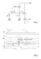
- Figure 1 schematically illustrates an exemplary circuit of a photosensitive cell of a matrix of photosensitive cells of an image sensor.
- Each photosensitive cell of the matrix is associated with a precharging device and a reading device.
- the precharging device consists of an NM channel NM transistor 1 , interposed between a supply rail Vdd and a read node S.
- the gate of the precharge transistor M 1 is adapted to receive a precharge control signal RST .
- the reading device consists of the series connection of first and second MOS transistors with channel NM 2 , M 3 .
- the drain of the first read transistor M 2 is connected to the supply rail Vdd.
- the source of the second read transistor M 3 is connected to an input terminal P of a processing circuit (not shown).
- the gate of the first read transistor M 2 is connected to the read node S.
- the gate of the second read transistor M 3 is adapted to receive a read signal RD.
- the photosensitive cell comprises a charge storage diode D 1 whose anode is connected to a source of a reference potential or ground of the GND circuit and the cathode is connected directly to the node S.
- the photosensitive cell comprises a photodiode D 2 whose anode is connected to the reference supply rail GND and the cathode is connected to the node S via an MOS transistor N-channel charge transfer M 4 .
- the gate of the transfer transistor M 4 is adapted to receive a charge transfer control signal T.
- the signals RD, RST, and T are provided by control circuits not shown in FIG.
- the diode D 1 may not be realized by a specific component.
- the storage function of the charges coming from the photodiode D 2 is then ensured by the apparent capacitance at the reading node S which consists of the capacitances of the sources of the transistors M 1 and M 4 , the input capacitance of the transistor M 2 and than all the parasitic capacitances present at the node S.
- a photodetection cycle begins with a precharge phase during which a reference voltage level is imposed on the diode D 1 .
- This precharging is carried out by passing the precharging transistor M 1 .
- the precharge transistor M 1 is blocked.
- the state is then read at the node S, ie the actual reference state of charge of the diode D 1 .
- the cycle is continued by a transfer to the node S photogenerated charges, that is to say, created and stored in the presence of radiation, in the photodiode D 2 . This transfer is carried out by passing the transfer transistor M 4 .
- FIG. 2 schematically illustrates a photosensitive cell or pixel of a conventional image sensor intended to be illuminated by the front face. Only the photodiode D 2 and the transistor M 4 are represented.
- a substrate 1 of P type - there is provided a region 2 of P-type more highly doped than the substrate 1 and a doped region 3 N pinched between the region 2 and the substrate 1 corresponding to the photodiode D 2 which has a structure said pinch.
- the cell comprises a portion of polycrystalline silicon 4 disposed on an insulating portion 6, spacers 7 being provided on either side of the portions 4, 6.
- the polycrystalline silicon portion 4 corresponds to the gate of the transistor M 4 and the portion insulator 6 corresponds to the gate oxide of transistor M 4 .
- an N-type region 8 corresponding to the reading node of the photosensitive cell.
- Metal interconnections in the form of tracks and metal vias 9, are formed at a stack of insulating layers 11 covering the substrate 1 and are connected to the components of the cell.
- the cell also comprises a color filter 12 covering the stack of insulating layers 11 on which a microlens 13 is disposed.
- the light rays that reach the microlens 13 are focused towards the photodiode D 2 .
- incident light rays can be deflected or blocked by the interconnections 9 and not reach the photodiode D 2 .
- the current trend is to reduce the size of the photosensitive cells, the problem of the presence of metal interconnections 9 becomes even more important. To overcome this problem, it has been imagined a lighting of the photodiode D 2 by the rear face of the substrate 1.
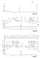
- FIGS. 3A to 3D schematically illustrate steps of an exemplary conventional method of manufacturing an image sensor illuminated by the rear face.
- FIG. 3A shows a strongly doped P-type substrate 14 on which a P-type monocrystalline silicon layer 15 has been epitaxially grown which is less heavily doped than the substrate 14.
- the layer 15 comprises a front face 16 and a, by for example, a thickness of about 3 microns.
- FIG. 3B represents the structure obtained after having made at the level of the layer 15 the components associated with the pixels. In FIG. 3B, two adjacent pixels are represented. The elements common to the pixel represented in FIG. 2 are designated with the same references. To insure the insulation between the two pixels, an insulation zone 17 has been formed in the layer 15, for example made of silicon oxide.
- FIG. 3A shows a strongly doped P-type substrate 14 on which a P-type monocrystalline silicon layer 15 has been epitaxially grown which is less heavily doped than the substrate 14.
- the layer 15 comprises a front face 16 and a, by for
- FIG. 3C represents the structure obtained after having made the levels of interconnections 9 in the stack of insulating layers 11 covering the layer 15 and after having stuck on the stack of insulating layers 11 a second substrate 18 on which it has grown a silicon oxide layer 19.
- FIG. 3D represents the structure obtained after removing the substrate 14, for example by a chemical-mechanical polishing process, to define a rear face 20 of the layer 15 and after having realized on the rear face 20 of the color filters 21 and 22 and microlenses 23 and 24.
- a disadvantage of the image sensor structure shown in FIG. 3D results from the scattering of electrons in the layer 15.
- the incident photons cause the formation in the electron / hole pair layer 15, the electrons forming in a portion of the layer 15 associated with a photosensitive cell to be captured by the photodiode of this cell.
- certain electrons resulting from the absorption of photons in a portion of the layer 15 associated with a cell photosensitive data can be captured by the photodiodes of adjacent photosensitive cells. This results in undesirable noise on the signals measured at the reading nodes whose amplitude varies for each photosensitive cell.
- Such a phenomenon is due to the scattering of electrons forming in a portion of the layer 15 associated with a given photosensitive cell to the photodiodes of adjacent cells rather than to the photodiode of the given photosensitive cell.
- the risk of diffusion of electrons towards adjacent cells is all the more important as the place of formation of the electrons is remote from the photodiodes.
- the photons whose wavelengths correspond to blue or green are mainly absorbed in the first two micrometers of the substrate 1. Due to the focusing of the light rays by the lens 13, the electrons resulting from the absorption of such photons are formed mainly near the photodiode D 2 . The risk that some of these electrons diffuse to the adjacent photosensitive cells is therefore low. Only the photons whose wavelength corresponds to red can be absorbed over a greater thickness of the substrate 1. The risk that some of these electrons diffuse towards the adjacent cells is then greater, but the overall number of electrons likely to spread to adjacent cells remains weak.
- the risk of diffusion of electrons towards the adjacent photosensitive cells is greater.
- the electrons that are most likely to diffuse to the adjacent photosensitive cells are those that form in the first two micrometers of the layer 15 from the rear face 20.
- the number of these electrons is greater than for a sensor images illuminated by the front as they come from the absorption of photons corresponding to blue, green and red colors.
- the disturbance of the signals measured due to the diffusion of electrons towards the adjacent photosensitive cells is therefore more important for a rear-illuminated image sensor.
- An object of the present invention is to provide an image sensor illuminated by the rear face to reduce or eliminate the diffusion of electrons associated with a given pixel to adjacent pixels.
- Another object of the present invention is to provide a method of manufacturing an image sensor illuminated by the rear face to reduce or eliminate the diffusion of electrons associated with a given pixel to adjacent pixels.
- one aspect of the present invention provides an image sensor comprising a layer of a P-type doped semiconductor material having first and second opposing faces; and at least one photodiode formed in the layer on the side of the first face and intended to be illuminated by the second face.
- the dopant concentration of the layer increases from the first face to the second face.
- the increase in the dopant concentration of the layer is substantially continuous.
- the dopant concentration of the layer increases in successive stages.
- the dopant concentration of the layer is substantially constant over a given thickness from the first face.
- the thickness given is 1 ⁇ m.
- the thickness of the layer is between 2 microns and 4 microns.
- Another aspect of the present invention provides a device, in particular a mobile phone, a camera, a camcorder, a digital microscope or a digital camera, comprising an image sensor as previously defined.
- Another aspect of the present invention provides a method of manufacturing an image sensor comprising the steps of forming a layer of a P-type doped semiconductor material having first and second opposing faces, the dopant concentration. the layer increasing from the first face to the second face; and forming in the layer at least one photodiode on the side of the first face and intended to be illuminated by the second face.
- the layer is formed by epitaxy.
- the layer is formed on an insulating layer covering a substrate, the substrate and at least a portion of said insulating layer being removed after forming said photodiode.
- FIG. 4 is a figure similar to FIG. 3D and represents an exemplary embodiment of an image sensor according to the invention.
- the lightly doped P-type layer 15 has been replaced by a p-type doped silicon layer 26 whose dopant concentration increases from the front face 16 of the layer 26 to the 20.
- the thickness of the layer 26 may vary between 2 microns and 6 microns and the dopant concentration may vary from a few 14 atoms / cm 3 near the front face 16 to a few 10 17 atoms / cm 3 near the back face 20.
- the dopant used is of type P, and corresponds, for example, to boron.
- the arrows 27 illustrate the dopant concentration gradient in the layer 26.
- the manufacturing method of the present exemplary embodiment of the image sensor according to the invention can be analogous to the method previously described in relation to FIGS. 3A to 3D, the layer 26 is produced by epitaxy on the substrate 14. It is then expected, simultaneously with the epitaxial growth of the layer 26, to perform a P-type doping whose concentration increases in the direction of the arrows 27.
- the dopant concentration gradient causes the formation of an electrostatic field in the oriented layer 26 as the concentration gradient. This results in the exercise of a force on the electrons forming in the layer 26 oriented in the direction opposite to the arrows 27. The electrons are thus led to the photodiode D 2 associated with the portion of the layer 26 of the pixel in which they are trained. The electrostatic field thus prevents the electrons from diffusing towards the neighboring pixels.
- the increase in the dopant concentration can be carried out continuously and regularly from the front face 16 to the rear face 20 of the layer 26.
- the increase in the concentration can be straight.
- the dopant concentration in the layer 26 may be constant over a given thickness from the front face 16 of the layer 26 and then increase up to the rear face 20.
- the thickness given may be of the order of 1 ⁇ m. This advantageously makes it possible to maintain the dopant concentration constant at the portions of the layer 26 corresponding to the channel regions of the transistors of the photosensitive cells. Indeed, the electrical focusing of a MOS transistor to optimize its operation is very sensitive and is generally performed considering that the silicon portion in which the transistor is formed has a constant dopant concentration. It may therefore be advantageous to have a constant dopant concentration at each transistor of the photosensitive cell so as not to modify the operating point of this transistor and in particular the transistor channel formation conditions.
- the isolation zone 17 may correspond to a P-type region that is more heavily doped than the layer 26.
- the isolation zone 17 may be formed by one or more implantation steps. It can extend from the front face 16 to the given thickness on which the dopant concentration in the layer 26 is constant.
- the layer 26 it is possible to use, for the formation of the layer 26, a structure of the SOI type (acronym for Silicon On Insulator).
- a structure of the SOI type (acronym for Silicon On Insulator).
- the layer of silicon 26 with a variable dopant concentration can be produced by epitaxy on the tie layer.
- variable dopant concentration layer 26 can then be made by strongly doping the bonding layer on the insulating layer of the SOI structure and by epitaxially growing the layer 26 on the tie layer by constant dopant concentration. During the epitaxy, then, an exo-diffusion of the dopants from the tie layer occurs in the layer 26.
- FIG. 5 illustrates an example of use of the image sensor according to the invention.
- FIG. 5 schematically shows a mobile phone 31 comprising a housing 32 at which a screen 33 and a keyboard 34 are arranged.
- the mobile phone also comprises an image acquisition system 36 comprising an optical system controlling the light rays towards an image sensor according to the invention.
- the present invention is susceptible of various variations and modifications which will be apparent to those skilled in the art.
- the present invention also applies to a photosensitive cell for which several photodiodes are connected to the same reading node.
- the present invention has been described for an image sensor cell in which the precharging device and the reading device have a particular structure, the present invention also applies to a cell for which the The preload or the reading device have a different structure, for example comprise a different number of MOS transistors.
Abstract
Description
La présente invention concerne le domaine des capteurs d'images destinés à être utilisés dans des téléphones portables, des caméras, des caméscopes ou des appareils photographiques numériques. Elle concerne plus particulièrement des capteurs d'images réalisés de façon monolithique à base de matériaux semi-conducteurs.The present invention relates to the field of image sensors for use in mobile phones, cameras, camcorders or digital cameras. It relates more particularly to image sensors made monolithically based on semiconductor materials.
La figure 1 illustre schématiquement un exemple de circuit d'une cellule photosensible d'une matrice de cellules photosensibles d'un capteur d'images. A chaque cellule photosensible de la matrice sont associés un dispositif de précharge et un dispositif de lecture. Le dispositif de précharge est constitué d'un transistor MOS à canal N M1, interposé entre un rail d'alimentation Vdd et un noeud de lecture S. La grille du transistor de précharge M1 est propre à recevoir un signal de commande de précharge RST. Le dispositif de lecture est constitué de la connexion en série de premier et second transistors MOS à canal N M2, M3. Le drain du premier transistor de lecture M2 est connecté au rail d'alimentation Vdd. La source du second transistor de lecture M3 est connectée à une borne d'entrée P d'un circuit de traitement (non représenté). La grille du premier transistor de lecture M2 est reliée au noeud de lecture S. La grille du deuxième transistor de lecture M3 est propre à recevoir un signal de lecture RD. La cellule photosensible comprend une diode de stockage de charge D1 dont l'anode est reliée à une source d'un potentiel de référence ou masse du circuit GND et la cathode est reliée directement au noeud S. La cellule photosensible comprend une photodiode D2 dont l'anode est reliée au rail d'alimentation de référence GND et la cathode est reliée au noeud S par l'intermédiaire d'un transistor MOS à canal N de transfert de charges M4. La grille du transistor de transfert M4 est propre à recevoir un signal de commande de transfert de charges T. De façon générale, les signaux RD, RST, et T sont fournis par des circuits de commande non représentés en figure 1 et peuvent être fournis à l'ensemble des cellules photosensibles d'une même rangée de la matrice de cellules. La diode D1 peut ne pas être réalisée par un composant spécifique. La fonction de stockage des charges issues de la photodiode D2 est alors assurée par la capacité apparente au noeud de lecture S qui est constituée des capacités des sources des transistors M1 et M4, de la capacité d'entrée du transistor M2 ainsi que de l'ensemble des capacités parasites présentes au noeud S.Figure 1 schematically illustrates an exemplary circuit of a photosensitive cell of a matrix of photosensitive cells of an image sensor. Each photosensitive cell of the matrix is associated with a precharging device and a reading device. The precharging device consists of an NM channel NM transistor 1 , interposed between a supply rail Vdd and a read node S. The gate of the precharge transistor M 1 is adapted to receive a precharge control signal RST . The reading device consists of the series connection of first and second MOS transistors with channel NM 2 , M 3 . The drain of the first read transistor M 2 is connected to the supply rail Vdd. The source of the second read transistor M 3 is connected to an input terminal P of a processing circuit (not shown). The gate of the first read transistor M 2 is connected to the read node S. The gate of the second read transistor M 3 is adapted to receive a read signal RD. The photosensitive cell comprises a charge storage diode D 1 whose anode is connected to a source of a reference potential or ground of the GND circuit and the cathode is connected directly to the node S. The photosensitive cell comprises a photodiode D 2 whose anode is connected to the reference supply rail GND and the cathode is connected to the node S via an MOS transistor N-channel charge transfer M 4 . The gate of the transfer transistor M 4 is adapted to receive a charge transfer control signal T. In general, the signals RD, RST, and T are provided by control circuits not shown in FIG. 1 and can be provided. to the set of photosensitive cells of the same row of the matrix of cells. The diode D 1 may not be realized by a specific component. The storage function of the charges coming from the photodiode D 2 is then ensured by the apparent capacitance at the reading node S which consists of the capacitances of the sources of the transistors M 1 and M 4 , the input capacitance of the transistor M 2 and than all the parasitic capacitances present at the node S.
Le fonctionnement de ce circuit va maintenant être décrit. Un cycle de photodétection commence par une phase de précharge pendant laquelle on impose à la diode D1 un niveau de tension de référence. Cette précharge s'effectue en rendant passant le transistor de précharge M1. Une fois la précharge effectuée, le transistor de précharge M1 est bloqué. On lit alors l'état au noeud S, c'est à dire l'état de charge de référence réel de la diode D1. Le cycle se poursuit par un transfert vers le noeud S des charges photogénérées, c'est-à-dire créées et stockées en présence d'un rayonnement, dans la photodiode D2. Ce transfert s'effectue en rendant passant le transistor de transfert M4. Le transfert fini, le transistor M4 est bloqué et la photodiode D2 recommence à photogénérer et stocker des charges qui seront ultérieurement transférées vers le noeud S. Simultanément, à la fin du transfert, on lit le nouvel état de charge de la diode D2. Le signal de sortie transmis à la borne P dépend alors du pincement du canal du premier transistor de lecture M2, qui est directement fonction de la charge stockée dans la photodiode.The operation of this circuit will now be described. A photodetection cycle begins with a precharge phase during which a reference voltage level is imposed on the diode D 1 . This precharging is carried out by passing the precharging transistor M 1 . Once the precharging is done, the precharge transistor M 1 is blocked. The state is then read at the node S, ie the actual reference state of charge of the diode D 1 . The cycle is continued by a transfer to the node S photogenerated charges, that is to say, created and stored in the presence of radiation, in the photodiode D 2 . This transfer is carried out by passing the transfer transistor M 4 . The finite transfer, the transistor M 4 is blocked and the photodiode D 2 starts to photogenerate and storing charges which will be subsequently transferred to node S. Simultaneously, at the end of the transfer, we read the new charge state of diode D 2. The output signal transmitted to the terminal P then depends on the pinch of the channel of the first read transistor M 2 , which is a direct function of the charge stored in the photodiode.
La figure 2 illustre schématiquement une cellule photosensible ou pixel d'un capteur d'images classique destiné à être éclairé par la face avant. Seuls la photodiode D2 et le transistor M4 sont représentés. Dans un substrat 1 de type P-, on prévoit une région 2 de type P plus fortement dopée que le substrat 1 et une région 3 dopée N pincée entre la région 2 et le substrat 1 qui correspondent à la photodiode D2 qui a une structure dite pincée. La cellule comprend une portion de silicium polycristallin 4 disposée sur une portion isolante 6, des espaceurs 7 étant prévus de part et d'autre des portions 4, 6. La portion de silicium polycristallin 4 correspond à la grille du transistor M4 et la portion isolante 6 correspond à l'oxyde de grille du transistor M4. On prévoit, dans le substrat 1, une région 8 de type N correspondant au noeud de lecture de la cellule photosensible. Des interconnexions métalliques, sous forme de pistes et de vias métalliques 9, sont formées au niveau d'un empilement de couches isolantes 11 recouvrant le substrat 1 et sont reliées aux composants de la cellule. La cellule comprend également un filtre coloré 12 recouvrant l'empilement de couches isolantes 11 sur lequel une microlentille 13 est disposée.FIG. 2 schematically illustrates a photosensitive cell or pixel of a conventional image sensor intended to be illuminated by the front face. Only the photodiode D 2 and the transistor M 4 are represented. In a
Les rayons lumineux qui atteignent la microlentille 13 sont focalisés vers la photodiode D2. Toutefois, des rayons lumineux incidents peuvent être déviés ou bloqués par les interconnexions 9 et ne pas atteindre la photodiode D2. En outre, la tendance actuelle étant à la réduction des dimensions des cellules photosensibles, le problème de la présence des interconnexions métalliques 9 devient d'autant plus important. Pour pallier à ce problème, il a été imaginé un éclairage de la photodiode D2 par la face arrière du substrat 1.The light rays that reach the
Les figures 3A à 3D illustrent schématiquement des étapes d'un exemple de procédé classique de fabrication d'un capteur d'images éclairé par la face arrière. La figure 3A représente un substrat 14 de type P fortement dopé sur lequel a été réalisée par épitaxie une couche 15 de silicium mono- cristallin de type P moins fortement dopée que le substrat 14. La couche 15 comprend une face avant 16 et a, par exemple, une épaisseur d'environ 3 µm. La figure 3B représente la structure obtenue après avoir réalisé au niveau de la couche 15 les composants associés aux pixels. En figure 3B, on a représenté deux pixels adjacents. Les éléments communs au pixel représenté en figure 2 sont désignés avec les mêmes références. Pour assurer l'isolation entre les deux pixels, on a réalisé dans la couche 15 une zone d'isolation 17, par exemple en oxyde de silicium. La figure 3C représente la structure obtenue après avoir réalisé les niveaux d'interconnexions 9 dans l'empilement de couches isolantes 11 recouvrant la couche 15 et après avoir collé sur l'empilement de couches isolantes 11 un second substrat 18 sur lequel on a fait croître une couche d'oxyde de silicium 19. La figure 3D représente la structure obtenue après avoir retiré le substrat 14, par exemple par un procédé de polissage mécano-chimique, pour définir une face arrière 20 de la couche 15 et après avoir réalisé sur la face arrière 20 des filtres de couleur 21 et 22 et des microlentilles 23 et 24.FIGS. 3A to 3D schematically illustrate steps of an exemplary conventional method of manufacturing an image sensor illuminated by the rear face. FIG. 3A shows a strongly doped P-
Un inconvénient de la structure de capteur d'images représentée sur la figure 3D résulte de la diffusion des électrons dans la couche 15. En effet, de façon générale, les photons incidents entraînent la formation dans la couche 15 de paires électron/trou, les électrons se formant dans une portion de la couche 15 associée à une cellule photosensible devant être capturés par la photodiode de cette cellule. Toutefois, on observe que certains électrons issus de l'absorption des photons dans une portion de la couche 15 associée à une cellule photosensible donnée peuvent être capturés par les photodiodes des cellules photosensibles adjacentes. Ceci se traduit par un bruit indésirable sur les signaux mesurés aux noeuds de lecture dont l'amplitude varie pour chaque cellule photosensible. Un tel phénomène est dû à la diffusion d'électrons se formant dans une portion de la couche 15 associée à une cellule photosensible donnée vers les photodiodes des cellules adjacentes plutôt que vers la photodiode de la cellule photosensible donnée. Le risque de diffusion d'électrons vers les cellules adjacentes est d'autant plus important que le lieu de formation des électrons est éloigné des photodiodes.A disadvantage of the image sensor structure shown in FIG. 3D results from the scattering of electrons in the
Lorsque le capteur d'images est éclairé par la face avant, ce phénomène est relativement peu important. En effet, les photons dont les longueurs d'onde correspondent au bleu ou au vert sont principalement absorbés dans les deux premiers micromètres du substrat 1. En raison de la focalisation des rayons lumineux par la lentille 13, les électrons issus de l'absorption de tels photons se forment principalement à proximité de la photodiode D2. Le risque que certains de ces électrons diffusent vers les cellules photosensibles adjacentes est donc faible. Seuls les photons dont la longueur d'onde correspond au rouge peuvent être absorbés sur une épaisseur plus importante du substrat 1. Le risque que certains de ces électrons diffusent vers les cellules adjacentes est alors plus important, mais le nombre global d'électrons susceptibles de diffuser vers des cellules adjacentes reste faible.When the image sensor is illuminated by the front panel, this phenomenon is relatively unimportant. Indeed, the photons whose wavelengths correspond to blue or green are mainly absorbed in the first two micrometers of the
Au contraire, lorsque le capteur d'images est éclairé par la face arrière, le risque de diffusion d'électrons vers les cellules photosensibles adjacentes est plus important. En effet, les électrons qui ont le plus de risque de diffuser vers les cellules photosensibles adjacentes sont ceux qui se forment dans les deux premiers micromètres de la couche 15 depuis la face arrière 20. Le nombre de ces électrons est plus important que pour un capteur d'images éclairé par la face avant puisqu'ils proviennent de l'absorption de photons correspondant aux couleurs bleue, verte et rouge. La perturbation des signaux mesurés en raison de la diffusion d'électrons vers les cellules photosensibles adjacentes est donc plus importante pour un capteur d'images éclairé par la face arrière.On the contrary, when the image sensor is illuminated by the rear face, the risk of diffusion of electrons towards the adjacent photosensitive cells is greater. Indeed, the electrons that are most likely to diffuse to the adjacent photosensitive cells are those that form in the first two micrometers of the
Un objet de la présente invention est de prévoir un capteur d'images éclairé par la face arrière permettant de réduire, voire de supprimer, la diffusion d'électrons associés à un pixel donné vers les pixels adjacents.An object of the present invention is to provide an image sensor illuminated by the rear face to reduce or eliminate the diffusion of electrons associated with a given pixel to adjacent pixels.
Un autre objet de la présente invention est de prévoir un procédé de fabrication d'un capteur d'images éclairé par la face arrière permettant de réduire, voire de supprimer, la diffusion d'électrons associés à un pixel donné vers les pixels adjacents.Another object of the present invention is to provide a method of manufacturing an image sensor illuminated by the rear face to reduce or eliminate the diffusion of electrons associated with a given pixel to adjacent pixels.
Pour atteindre tout ou partie de ces objets ainsi que d'autres, un aspect de la présente invention prévoit un capteur d'images comprenant une couche d'un matériau semi-conducteur dopée de type P comprenant des première et seconde faces opposées ; et au moins une photodiode formée dans la couche du côté de la première face et destinée à être éclairée par la seconde face. La concentration de dopants de la couche augmente de la première face vers la seconde face.To achieve all or part of these and other objects, one aspect of the present invention provides an image sensor comprising a layer of a P-type doped semiconductor material having first and second opposing faces; and at least one photodiode formed in the layer on the side of the first face and intended to be illuminated by the second face. The dopant concentration of the layer increases from the first face to the second face.
Selon un exemple de réalisation de la présente invention, l'augmentation de la concentration de dopants de la couche est sensiblement continue.According to an exemplary embodiment of the present invention, the increase in the dopant concentration of the layer is substantially continuous.
Selon un exemple de réalisation de la présente invention, la concentration de dopants de la couche augmente par paliers successifs.According to an exemplary embodiment of the present invention, the dopant concentration of the layer increases in successive stages.
Selon un exemple de réalisation de la présente invention, la concentration en dopants de la couche est sensiblement constante sur une épaisseur donnée depuis la première face.According to an exemplary embodiment of the present invention, the dopant concentration of the layer is substantially constant over a given thickness from the first face.
Selon un exemple de réalisation de la présente invention, l'épaisseur donnée est de 1 µm.According to an exemplary embodiment of the present invention, the thickness given is 1 μm.
Selon un exemple de réalisation de la présente invention, l'épaisseur de la couche est comprise entre 2 µm et 4 µm.According to an exemplary embodiment of the present invention, the thickness of the layer is between 2 microns and 4 microns.
Un autre aspect de la présente invention prévoit un dispositif, notamment un téléphone portable, une caméra, un caméscope, un microscope numérique ou un appareil photographique numérique, comprenant un capteur d'images tel que précédemment défini.Another aspect of the present invention provides a device, in particular a mobile phone, a camera, a camcorder, a digital microscope or a digital camera, comprising an image sensor as previously defined.
Un autre aspect de la présente invention prévoit un procédé de fabrication d'un capteur d'images comprenant les étapes consistant à former une couche d'un matériau semi-conducteur dopée de type P comprenant des première et seconde faces opposées, la concentration de dopants de la couche augmentant de la première face vers la seconde face ; et à former dans la couche au moins une photodiode du côté de la première face et destinée à être éclairée par la seconde face.Another aspect of the present invention provides a method of manufacturing an image sensor comprising the steps of forming a layer of a P-type doped semiconductor material having first and second opposing faces, the dopant concentration. the layer increasing from the first face to the second face; and forming in the layer at least one photodiode on the side of the first face and intended to be illuminated by the second face.
Selon un exemple de réalisation de la présente invention, la couche est formée par épitaxie.According to an exemplary embodiment of the present invention, the layer is formed by epitaxy.
Selon un exemple de réalisation de la présente invention, la couche est formée sur une couche isolante recouvrant un substrat, le substrat et au moins une partie de ladite couche isolante étant retirés après formation de ladite photodiode.According to an exemplary embodiment of the present invention, the layer is formed on an insulating layer covering a substrate, the substrate and at least a portion of said insulating layer being removed after forming said photodiode.
Ces objets, caractéristiques et avantages, ainsi que d'autres de la présente invention seront exposés en détail dans la description suivante d'un exemple de réalisation particulier faite à titre non-limitatif en relation avec les figures jointes parmi lesquelles :
- la figure 1, précédemment décrite, représente un schéma électrique d'une cellule photosensible ;
- la figure 2, précédemment décrite, représente un capteur d'images classique éclairé par la face avant ;
- les figures 3A à 3D, précédemment décrites, illustrent les étapes successives d'un procédé classique de fabrication d'un capteur d'images éclairé par la face arrière ;
- la figure 4 représente un exemple de réalisation d'un capteur d'images éclairé par la face arrière selon l'invention ; et
- la figure 5 représente, de façon schématique, un téléphone portable comprenant un capteur d'images selon l'invention.
- Figure 1, previously described, shows an electrical diagram of a photosensitive cell;
- FIG. 2, previously described, represents a conventional image sensor illuminated by the front face;
- FIGS. 3A to 3D, previously described, illustrate the successive steps of a conventional method of manufacturing an image sensor illuminated by the rear face;
- FIG. 4 represents an exemplary embodiment of an image sensor illuminated by the rear face according to the invention; and
- FIG. 5 schematically represents a mobile phone comprising an image sensor according to the invention.
Par souci de clarté, de mêmes éléments ont été désignés par de mêmes références aux différentes figures et, de plus, comme cela est habituel dans la représentation des circuits intégrés, les diverses figures ne sont pas tracées à l'échelle.For the sake of clarity, the same elements have been designated by the same references in the various figures and, moreover, as is customary in the representation of the integrated circuits, the various figures are not drawn to scale.
La figure 4 est une figure analogue à la figure 3D et représente un exemple de réalisation d'un capteur d'images selon l'invention. Par rapport au capteur d'images représenté en figure 3D, la couche 15 de type P faiblement dopée a été remplacée par une couche 26 de silicium dopée de type P dont la concentration en dopants augmente depuis la face avant 16 de la couche 26 jusqu'à la face arrière 20. A titre d'exemple, l'épaisseur de la couche 26 peut varier entre 2 µm et 6 µm et la concentration en dopants peut varier de quelques 1014 atomes/cm3 près de la face avant 16 à quelques 1017 atomes/cm3 près de la face arrière 20. Le dopant utilisé est de type P, et correspond par exemple, au bore. Les flèches 27 illustrent le gradient de concentration de dopants dans la couche 26. Le procédé de fabrication du présent exemple de réalisation du capteur d'images selon l'invention peut être analogue au procédé précédemment décrit en relation aux figures 3A à 3D, la couche 26 étant réalisée par épitaxie sur le substrat 14. On prévoit alors, simultanément à la croissance épitaxiale de la couche 26, de réaliser un dopage de type P dont la concentration augmente dans le sens des flèches 27.FIG. 4 is a figure similar to FIG. 3D and represents an exemplary embodiment of an image sensor according to the invention. With respect to the image sensor shown in FIG. 3D, the lightly doped P-
Le gradient de concentration de dopants entraîne la formation d'un champ électrostatique dans la couche 26 orienté comme le gradient de concentration. Ceci se traduit par l'exercice d'une force sur les électrons se formant dans la couche 26 orientée dans le sens opposé aux flèches 27. Les électrons sont donc conduits vers la photodiode D2 associée à la portion de la couche 26 du pixel dans laquelle ils se sont formés. Le champ électrostatique empêche donc les électrons de diffuser vers les pixels voisins.The dopant concentration gradient causes the formation of an electrostatic field in the oriented
L'augmentation de la concentration de dopants peut être effectuée de manière continue et régulière de la face avant 16 vers la face arrière 20 de la couche 26. A titre d'exemple, l'augmentation de la concentration peut être rectiligne.The increase in the dopant concentration can be carried out continuously and regularly from the
La concentration de dopants dans la couche 26 peut être constante sur une épaisseur donnée depuis la face avant 16 de la couche 26 puis augmenter jusqu'à la face arrière 20. L'épaisseur donnée peut être de l'ordre de 1 µm. Ceci permet avantageusement de maintenir la concentration de dopants constante au niveau des portions de la couche 26 correspondant aux régions de canal des transistors des cellules photosensibles. En effet, la mise au point électrique d'un transistor MOS afin d'optimiser son fonctionnement est très sensible et est généralement réalisée en considérant que la portion de silicium dans laquelle est formé le transistor a une concentration de dopants constante. Il peut donc être avantageux d'avoir une concentration de dopants constante au niveau de chaque transistor de la cellule photosensible pour ne pas modifier le point de fonctionnement de ce transistor et notamment les conditions de formation du canal du transistor.The dopant concentration in the
Selon une variante de la présente invention, la zone d'isolation 17 peut correspondre à une région de type P plus fortement dopée que la couche 26. La zone d'isolation 17 peut être formée par une ou plusieurs étapes d'implantation. Elle peut s'étendre depuis la face avant 16 sur l'épaisseur donnée sur laquelle la concentration de dopants dans la couche 26 est constante.According to a variant of the present invention, the
Selon un mode de mise en oeuvre de la présente invention, on peut utiliser, pour la formation de la couche 26, une structure du type SOI (acronyme anglais pour Silicon On Insulator). On part de la couche de silicium supérieure de la structure SOI, qui constitue une couche d'accroche. La couche de silicium 26 à concentration de dopants variable peut être réalisée par épitaxie sur la couche d'accroche.According to an embodiment of the present invention, it is possible to use, for the formation of the
Selon une variante de mise en oeuvre, on part de la couche de silicium supérieure d'une structure SOI, qui constitue de nouveau une couche d'accroche. La couche 26 à concentration de dopants variable peut alors être réalisée en dopant fortement la couche d'accroche sur la couche isolante de la structure SOI et en faisant croître par épitaxie à concentration de dopants constante la couche 26 sur la couche d'accroche. Il se produit alors, pendant l'épitaxie, une exo-diffusion des dopants, à partir de la couche d'accroche, dans la couche 26.According to an alternative embodiment, one starts from the upper silicon layer of an SOI structure, which again constitutes a tie layer. The variable
La figure 5 illustre un exemple d'utilisation du capteur d'images selon l'invention. La figure 5 représente, de façon schématique, un téléphone portable 31 comprenant un boîtier 32 au niveau duquel sont disposés un écran 33 et un clavier 34. Le téléphone portable comprend également un système d'acquisition d'images 36 comportant un système optique dirigeant les rayons lumineux vers un capteur d'images selon l'invention.FIG. 5 illustrates an example of use of the image sensor according to the invention. FIG. 5 schematically shows a
Bien entendu, la présente invention est susceptible de diverses variantes et modifications qui apparaîtront à l'homme de l'art. En particulier, la présente invention s'applique également à une cellule photosensible pour laquelle plusieurs photodiodes sont reliées à un même noeud de lecture. En outre, bien que la présente invention ait été décrite pour une cellule de capteurs d'images dans laquelle le dispositif de précharge et le dispositif de lecture ont une structure particulière, la présente invention s'applique également à une cellule pour laquelle le dispositif de précharge ou le dispositif de lecture ont une structure différente, par exemple comprennent un nombre différent de transistors MOS.Of course, the present invention is susceptible of various variations and modifications which will be apparent to those skilled in the art. In particular, the present invention also applies to a photosensitive cell for which several photodiodes are connected to the same reading node. Furthermore, although the present invention has been described for an image sensor cell in which the precharging device and the reading device have a particular structure, the present invention also applies to a cell for which the The preload or the reading device have a different structure, for example comprise a different number of MOS transistors.
Claims (10)
Applications Claiming Priority (1)
| Application Number | Priority Date | Filing Date | Title |
|---|---|---|---|
| FR0652817 | 2006-07-05 |
Publications (1)
| Publication Number | Publication Date |
|---|---|
| EP1876647A2 true EP1876647A2 (en) | 2008-01-09 |
Family
ID=37814652
Family Applications (1)
| Application Number | Title | Priority Date | Filing Date |
|---|---|---|---|
| EP07111519A Withdrawn EP1876647A2 (en) | 2006-07-05 | 2007-07-02 | Back-illuminated image sensor |
Country Status (2)
| Country | Link |
|---|---|
| US (1) | US20080017893A1 (en) |
| EP (1) | EP1876647A2 (en) |
Families Citing this family (5)
| Publication number | Priority date | Publication date | Assignee | Title |
|---|---|---|---|---|
| US7888763B2 (en) * | 2008-02-08 | 2011-02-15 | Omnivision Technologies, Inc. | Backside illuminated imaging sensor with improved infrared sensitivity |
| KR20100000161A (en) * | 2008-06-24 | 2010-01-06 | 삼성전자주식회사 | An align key method for cmos image sensor having backside illumination structure |
| JP5269527B2 (en) * | 2008-08-29 | 2013-08-21 | 株式会社東芝 | Semiconductor device |
| US9048162B2 (en) | 2012-05-31 | 2015-06-02 | Taiwan Semiconductor Manufacturing Company, Ltd. | CMOS image sensors and methods for forming the same |
| US9859311B1 (en) | 2016-11-28 | 2018-01-02 | Omnivision Technologies, Inc. | Storage gate protection |
Family Cites Families (5)
| Publication number | Priority date | Publication date | Assignee | Title |
|---|---|---|---|---|
| US6683360B1 (en) * | 2002-01-24 | 2004-01-27 | Fillfactory | Multiple or graded epitaxial wafers for particle or radiation detection |
| JP4211696B2 (en) * | 2004-06-30 | 2009-01-21 | ソニー株式会社 | Method for manufacturing solid-state imaging device |
| US8049293B2 (en) * | 2005-03-07 | 2011-11-01 | Sony Corporation | Solid-state image pickup device, electronic apparatus using such solid-state image pickup device and method of manufacturing solid-state image pickup device |
| US7381603B2 (en) * | 2005-08-01 | 2008-06-03 | Semiconductor Components Industries, L.L.C. | Semiconductor structure with improved on resistance and breakdown voltage performance |
| US20070045682A1 (en) * | 2005-08-31 | 2007-03-01 | Hong Sungkwon C | Imager with gradient doped EPI layer |
-
2007
- 2007-06-29 US US11/824,287 patent/US20080017893A1/en not_active Abandoned
- 2007-07-02 EP EP07111519A patent/EP1876647A2/en not_active Withdrawn
Also Published As
| Publication number | Publication date |
|---|---|
| US20080017893A1 (en) | 2008-01-24 |
Similar Documents
| Publication | Publication Date | Title |
|---|---|---|
| EP1883112B1 (en) | Back illuminated image sensor with an uniform substrate temperature | |
| EP2216817B1 (en) | Back side illuminated image sensor | |
| EP1873836B1 (en) | Back illuminated image sensor | |
| FR2820883A1 (en) | HIGH CAPACITY PHOTODIODE | |
| FR2930676A1 (en) | IMAGE SENSOR WITH VERY LOW DIMENSIONS | |
| EP2786412B1 (en) | Optical detector unit | |
| EP2587539B1 (en) | UTTB CMOS imager | |
| FR2888989A1 (en) | IMAGE SENSOR | |
| EP2355156B1 (en) | Photodiode for image sensor | |
| EP3016141A1 (en) | Image sensor with vertical electrodes | |
| FR2910710A1 (en) | Image sensor controlling device for e.g. digital camera, has bias circuit including switch to connect source of transistor to charge voltage for increasing potential of source of transistor, when photodiode is discharged toward node | |
| FR2974237A1 (en) | REAR-SIDED IMAGE SENSOR WITH TRANSPARENT ELECTRODE | |
| EP1876647A2 (en) | Back-illuminated image sensor | |
| FR2957193A1 (en) | SEOI SUBSTRATE DATA PATH CELL WITH REAR CONTROL GRID BURED UNDER THE INSULATING LAYER | |
| EP1231642A1 (en) | Three-transistor photodetector | |
| EP2312832B1 (en) | Pixel circuit in image sensor | |
| FR2844398A1 (en) | Monolithic photodetector for image sensor for devices, e.g. cameras, comprises first active area of doped single-crystal silicon corresponding to first and second photodiodes | |
| EP2846357A1 (en) | Photodetector device with semiconductor regions divided by a potential barrier | |
| FR2846147A1 (en) | Device and method for controlling a photosensitive cell of an image sensor, comprises generation of charge-transfer control signal with part slopes | |
| EP2947689B1 (en) | Photonic cmos inverter | |
| FR3046295A1 (en) | PIXEL WITH REAR FACE LIGHTING | |
| EP3163622B1 (en) | Photosensitive logic cell for illumination from the front | |
| FR2918795A1 (en) | IMAGE SENSOR WITH IMPROVED SENSITIVITY. | |
| FR2934926A1 (en) | MINIATURE IMAGE SENSOR. | |
| EP2909861A1 (en) | Image sensor having improved quantum efficiency at large wavelengths |
Legal Events
| Date | Code | Title | Description |
|---|---|---|---|
| PUAI | Public reference made under article 153(3) epc to a published international application that has entered the european phase |
Free format text: ORIGINAL CODE: 0009012 |
|
| AK | Designated contracting states |
Kind code of ref document: A2 Designated state(s): AT BE BG CH CY CZ DE DK EE ES FI FR GB GR HU IE IS IT LI LT LU LV MC MT NL PL PT RO SE SI SK TR |
|
| AX | Request for extension of the european patent |
Extension state: AL BA HR MK YU |
|
| STAA | Information on the status of an ep patent application or granted ep patent |
Free format text: STATUS: THE APPLICATION HAS BEEN WITHDRAWN |
|
| 18W | Application withdrawn |
Effective date: 20101105 |