EP1873581A2 - Display substrate and display device having the same - Google Patents
Display substrate and display device having the same Download PDFInfo
- Publication number
- EP1873581A2 EP1873581A2 EP07011550A EP07011550A EP1873581A2 EP 1873581 A2 EP1873581 A2 EP 1873581A2 EP 07011550 A EP07011550 A EP 07011550A EP 07011550 A EP07011550 A EP 07011550A EP 1873581 A2 EP1873581 A2 EP 1873581A2
- Authority
- EP
- European Patent Office
- Prior art keywords
- line
- signal
- pad
- display device
- conductive layer
- Prior art date
- Legal status (The legal status is an assumption and is not a legal conclusion. Google has not performed a legal analysis and makes no representation as to the accuracy of the status listed.)
- Withdrawn
Links
Images




Classifications
-
- G—PHYSICS
- G02—OPTICS
- G02F—OPTICAL DEVICES OR ARRANGEMENTS FOR THE CONTROL OF LIGHT BY MODIFICATION OF THE OPTICAL PROPERTIES OF THE MEDIA OF THE ELEMENTS INVOLVED THEREIN; NON-LINEAR OPTICS; FREQUENCY-CHANGING OF LIGHT; OPTICAL LOGIC ELEMENTS; OPTICAL ANALOGUE/DIGITAL CONVERTERS
- G02F1/00—Devices or arrangements for the control of the intensity, colour, phase, polarisation or direction of light arriving from an independent light source, e.g. switching, gating or modulating; Non-linear optics
- G02F1/01—Devices or arrangements for the control of the intensity, colour, phase, polarisation or direction of light arriving from an independent light source, e.g. switching, gating or modulating; Non-linear optics for the control of the intensity, phase, polarisation or colour
- G02F1/13—Devices or arrangements for the control of the intensity, colour, phase, polarisation or direction of light arriving from an independent light source, e.g. switching, gating or modulating; Non-linear optics for the control of the intensity, phase, polarisation or colour based on liquid crystals, e.g. single liquid crystal display cells
- G02F1/133—Constructional arrangements; Operation of liquid crystal cells; Circuit arrangements
- G02F1/1333—Constructional arrangements; Manufacturing methods
- G02F1/1345—Conductors connecting electrodes to cell terminals
-
- G—PHYSICS
- G02—OPTICS
- G02F—OPTICAL DEVICES OR ARRANGEMENTS FOR THE CONTROL OF LIGHT BY MODIFICATION OF THE OPTICAL PROPERTIES OF THE MEDIA OF THE ELEMENTS INVOLVED THEREIN; NON-LINEAR OPTICS; FREQUENCY-CHANGING OF LIGHT; OPTICAL LOGIC ELEMENTS; OPTICAL ANALOGUE/DIGITAL CONVERTERS
- G02F1/00—Devices or arrangements for the control of the intensity, colour, phase, polarisation or direction of light arriving from an independent light source, e.g. switching, gating or modulating; Non-linear optics
- G02F1/01—Devices or arrangements for the control of the intensity, colour, phase, polarisation or direction of light arriving from an independent light source, e.g. switching, gating or modulating; Non-linear optics for the control of the intensity, phase, polarisation or colour
- G02F1/13—Devices or arrangements for the control of the intensity, colour, phase, polarisation or direction of light arriving from an independent light source, e.g. switching, gating or modulating; Non-linear optics for the control of the intensity, phase, polarisation or colour based on liquid crystals, e.g. single liquid crystal display cells
- G02F1/133—Constructional arrangements; Operation of liquid crystal cells; Circuit arrangements
- G02F1/1333—Constructional arrangements; Manufacturing methods
- G02F1/1345—Conductors connecting electrodes to cell terminals
- G02F1/13458—Terminal pads
-
- G—PHYSICS
- G02—OPTICS
- G02F—OPTICAL DEVICES OR ARRANGEMENTS FOR THE CONTROL OF LIGHT BY MODIFICATION OF THE OPTICAL PROPERTIES OF THE MEDIA OF THE ELEMENTS INVOLVED THEREIN; NON-LINEAR OPTICS; FREQUENCY-CHANGING OF LIGHT; OPTICAL LOGIC ELEMENTS; OPTICAL ANALOGUE/DIGITAL CONVERTERS
- G02F1/00—Devices or arrangements for the control of the intensity, colour, phase, polarisation or direction of light arriving from an independent light source, e.g. switching, gating or modulating; Non-linear optics
- G02F1/01—Devices or arrangements for the control of the intensity, colour, phase, polarisation or direction of light arriving from an independent light source, e.g. switching, gating or modulating; Non-linear optics for the control of the intensity, phase, polarisation or colour
- G02F1/13—Devices or arrangements for the control of the intensity, colour, phase, polarisation or direction of light arriving from an independent light source, e.g. switching, gating or modulating; Non-linear optics for the control of the intensity, phase, polarisation or colour based on liquid crystals, e.g. single liquid crystal display cells
- G02F1/133—Constructional arrangements; Operation of liquid crystal cells; Circuit arrangements
- G02F1/136—Liquid crystal cells structurally associated with a semi-conducting layer or substrate, e.g. cells forming part of an integrated circuit
- G02F1/1362—Active matrix addressed cells
- G02F1/136286—Wiring, e.g. gate line, drain line
-
- G—PHYSICS
- G02—OPTICS
- G02F—OPTICAL DEVICES OR ARRANGEMENTS FOR THE CONTROL OF LIGHT BY MODIFICATION OF THE OPTICAL PROPERTIES OF THE MEDIA OF THE ELEMENTS INVOLVED THEREIN; NON-LINEAR OPTICS; FREQUENCY-CHANGING OF LIGHT; OPTICAL LOGIC ELEMENTS; OPTICAL ANALOGUE/DIGITAL CONVERTERS
- G02F1/00—Devices or arrangements for the control of the intensity, colour, phase, polarisation or direction of light arriving from an independent light source, e.g. switching, gating or modulating; Non-linear optics
- G02F1/01—Devices or arrangements for the control of the intensity, colour, phase, polarisation or direction of light arriving from an independent light source, e.g. switching, gating or modulating; Non-linear optics for the control of the intensity, phase, polarisation or colour
- G02F1/13—Devices or arrangements for the control of the intensity, colour, phase, polarisation or direction of light arriving from an independent light source, e.g. switching, gating or modulating; Non-linear optics for the control of the intensity, phase, polarisation or colour based on liquid crystals, e.g. single liquid crystal display cells
- G02F1/133—Constructional arrangements; Operation of liquid crystal cells; Circuit arrangements
- G02F1/136—Liquid crystal cells structurally associated with a semi-conducting layer or substrate, e.g. cells forming part of an integrated circuit
- G02F1/1362—Active matrix addressed cells
- G02F1/136286—Wiring, e.g. gate line, drain line
- G02F1/13629—Multilayer wirings
Definitions
- Embodiments of the present invention relate to a display substrate and a display device having the display substrate. More particularly, embodiments of the present invention relate to a display substrate and a display device having the display substrate providing a reduced line resistance.
- a liquid crystal display device includes a display panel for displaying an image by using an optical transmittance of a liquid crystal, and a gate driving circuit and a source driving circuit that are electrically connected with the display panel.
- the display panel includes a plurality of pixel parts. Each of the pixel parts includes a switching element and a liquid crystal capacitor electrically connected with the switching element.
- the gate driving circuit outputs a gate signal to turn on the switching element.
- the source driving circuit outputs a data signal to drive the liquid crystal capacitor.
- a gate driving circuit and a source driving circuit formed as a chip may be directly mounted on the display panel for manufacturing a lighter, thinner, shorter, and smaller liquid crystal display device.
- signal lines transmitting driving signals to the chip are formed directly on the display panel.
- a signal delay may be induced due to a line resistance of the signal lines, where the signal delay degrades the display quality.
- a display substrate capable of reducing a line resistance.
- a display device having the display substrate is also provided. More particularly, in a display substrate according to an exemplary embodiment, the display substrate includes a plurality of pixel parts, a signal line part and a signal pad part. The pixel parts are formed in a display area.
- the signal line part is formed in a peripheral area surrounding the display area.
- the signal line part includes a first line formed with a first conductive layer, and a second line formed with a second conductive layer over the first line. The second line overlaps the first line.
- the signal pad part includes a first pad integrally formed with the first line, and a second pad integrally formed with the second line.
- the display device includes a plurality of pixel parts, a signal line part and a signal pad part.
- the pixel parts are formed in a display area.
- the signal line part is formed in a peripheral area surrounding the display area.
- the signal line part includes a first line formed with a first conductive layer, and a second line formed with a second conductive layer over the first line.
- the second line overlaps the first line.
- the signal pad part includes a first pad integrally formed with the first line, and a second pad integrally formed with the second line.
- FIG. 1 is a plan view illustrating a display device according to a first exemplary embodiment of the present invention.
- the display device includes a printed circuit board 100, a display panel 400, a source driving part 510, and a gate driving part 610.
- a main driving circuit 110 is mounted on the printed circuit board 100.
- the printed circuit board 100 is electrically connected with the display panel 400 through the source driving part 510.
- the source driving part 510 includes first, second, third, fourth, fifth, sixth, seventh and eighth source tape carrier packages 511, 512, 513, 514, 515, 516, 517 and 518.
- the gate driving part 610 includes first, second and third gate tape carrier packages 611, 612 and 613.
- the tape carrier package (hereinafter, 'TCP') is a flexible printed circuit board on which a driving chip is mounted.
- a first line part 120 transmits a source driving signal to the source driving part 510.
- a second line part 131 transmits a data signal to the first, second, third and fourth source TCPs 511, 512, 513 and 514 disposed at a left side of the display panel 400.
- a third line part 132 transmits a data signal to the fifth, sixth, seventh and eighth source TCPs 515, 516, 517 and 518 disposed at a right side of the display panel 400.
- the fourth line part 140 transmits a gate driving signal to the first, second and third gate TCPs 611, 612 and 613.
- the display panel 400 includes a display substrate 200 and an opposite substrate 300 to be combined with the display substrate 200 to receive a liquid crystal layer (not illustrated).
- the display panel 400 includes a display area DA displaying an image, and first and second peripheral areas PA1 and PA2 surrounding the display area DA.
- a plurality of source lines DL and a plurality of gate lines GL crossing the source lines DL are formed in the display area DA.
- the source lines DL and the gate lines GL define a plurality of pixel parts 'P'.
- a switching element TFT, a liquid crystal capacitor CLC and a storage capacitor CST are formed in each of the pixel parts 'P'.
- the source driving part 510 is mounted in the first peripheral area PA1.
- the first, second, third and fourth source TCPs 511, 512, 513 and 514 are mounted at a left side of the first peripheral area PA1
- the fifth, sixth, seventh and eighth source TCPs 515, 516, 517 and 518 are mounted at a right side of the first peripheral area PA1.
- a first signal line part 210 applying a source driving signal to the source driving part 510 is formed in the first peripheral area PA1.
- the first signal line part 210 is formed between the neighboring source TCPs.
- the first signal line part 210 transmits the source driving signal to the first, second, third, fourth, fifth, sixth, seventh and eighth source tape carrier packages 511, 512, 513, 514, 515, 516, 517 and 518 in a cascade mode.
- the source driving signal may be a driving voltage VDD or VSS for driving a source driving chip mounted on the source TCP.
- the first signal line part 210 may include a power line and a ground line.
- the first signal line part 210 may include stacked metal layers that are insulated from each other.
- the gate driving part 610 is mounted on the second peripheral area PA2.
- the first, second and third gate TCPs 611, 612 and 613 are mounted on the second peripheral area PA2.
- a second signal line part 220 which transmits a gate driving signal to the first, second and third gate TCPs 611, 612 and 613, is formed in the second peripheral area PA2.
- the second signal line part 220 is formed between the neighboring source TCPs.
- the second signal line part 220 transmits the gate driving signal to the first, second and third gate TCPs 611, 612 and 613 in a cascade mode.
- the gate driving signal may be a gate voltage VON or VOFF.
- the second signal line part 220 may include a power line and a ground line.
- the second signal line part 220 may include stacked metal layers that are insulated from each other.
- FIG. 2A is a partially enlarged plan view illustrating the first peripheral area in FIG. 1.
- FIG. 2B is a partially enlarged plan view illustrating the second peripheral area in FIG. 1.
- the first peripheral area PA1 is sectioned into a first mounting area CA1 and a first separating area IA1 positioned between the neighboring first mounting areas CA1.
- the source TCPs are mounted on the first mounting area CA1.
- a first input-output pad part IOP1 electrically connected with input-output terminals of the source TCPs is formed in the first mounting area CA1.
- the first signal line part 210 for transmitting the source driving signal in a cascade mode is formed in the first separating area IA1.
- the first input-output pad part IOP1 includes a source pad part DP and a first signal pad part SP1.
- the source pad part DP is electrically connected with a first fan out part F01 and applies the data signal to the source lines DL.
- the first signal pad part SP1 is electrically connected with the first signal line part 210.
- the first signal line part 210 includes a power line 211 transmitting a power voltage VDD and a ground line 213 transmitting a ground voltage VSS.
- the first signal line part 210 may have a vertical multiplex or interleaved structure, for example, having a first line and a second line that are stacked such that the first and second lines are insulated from each other.
- the first signal pad part SP1 may have a horizontal multiplex structure that includes a first pad integrally formed with the first line and a second pad integrally formed with the second line.
- the second peripheral area PA2 is sectioned into a second mounting area CA2 and a second separating area IA2.
- the gate TCPs are mounted on the second mounting area CA2.
- a second input-output pad part IOP2 electrically connected with input-output terminals of the gate TCPs is formed in the second mounting area CA2.
- the second signal line part 220 for transmitting the gate driving signal in a cascade mode is formed in the second separating area IA2.
- the second input-output pad part IOP2 includes a gate pad part GP and a second signal pad part SP2.
- the gate pad part GP is electrically connected with a second fan out part FO2 and applies the gate signal to the gate lines GL.
- the second signal pad part SP2 is electrically connected with the second signal line part 220.
- the second signal line part 220 includes a power line 221 transmitting a gate on voltage VON and a ground line 223 transmitting a gate off voltage VOFF.
- the gate signal line part 220 may have a vertical multiplex structure, for example, having a first line and a second line that are stacked such that the first and second lines are insulated from each other.
- the second signal pad part SP2 may have a horizontal multiplex structure that includes a first pad integrally formed with the first line and a second pad integrally formed with the second line.
- the first and second signal line parts 210 and 220 are formed in a structure having a first line and a second line that are stacked such that the first and second lines are insulated from each other.
- Each of the first and second signal pad part SP1 and SP2 that are connected with the first and second signal line parts 210 and 220 respectively includes a first pad connected with the first line and a second pad connected with the second line.
- the exemplary embodiment of the present invention will be explained in more detail with referring to the second signal line part 220 and the second signal pad part SP2.
- FIG. 3 is an enlarged plan view illustrating the second signal line part and the second signal pad part in FIG. 2B.
- FIG. 4 is a partial cross-sectional view taken along a line I-I' and a line II-II' in FIG. 3.
- the signal line part includes the power line 221 and the ground line 223.
- the second signal line part includes a power pad part 222 formed at an end portion of the power line 221, and a ground pad part 224 formed at an end portion of the ground line 223.
- a first line 221 a of the power line 221 and a first pad 222a of the power pad part 222 are formed on a base substrate 201.
- the first pad 222a of the power pad part 222 is formed at an end portion of the first line 221 a.
- the first line 221 a and the first pad 222a are formed with a first conductive layer.
- the first conductive layer may be a gate metal layer forming the gate line GL and a gate electrode of the switching element TFT connected with the gate line GL.
- a gate insulating layer 202 is formed over the first line 221 a and the first pad 222a.
- a second line 221 b of the power line 221 is formed over the gate insulating layer 202 so that the second line 221 b overlaps with the first line 221 a.
- a second pad 222b of the power pad part 222 is formed at an end portion of the second line 221 b.
- the second line 221 b and the second pad 222b are formed with a second conductive layer.
- the second conductive layer may be a source metal layer forming the source line DL, a source electrode and a drain electrode of the switching element TFT.
- a passivation layer 203 is formed over the second line 221 b and the second pad 222b.
- a contact hole exposing the first and second pads 222a and 222b is formed at the passivation layer 203.
- a conductive pattern 222c electrically connected with the first and second pads 222a and 222b via the contact hole is formed on the passivation layer 203.
- the conductive pattern 222c is formed with a third conductive layer.
- the third conductive layer may be a transparent conductive layer forming a pixel electrode of the liquid crystal capacitor CLC electrically connected with the switching element TFT.
- the first line 221 a receives the gate on voltage VON through the first pad 222a
- the second line 221 b receives the gate on voltage VON through the second pad 222b.
- the power line 221 has a parallel connection resistance because the first line 221 a and the second line 221b are formed in parallel with each other. Therefore, the line resistance of the power line 221 may be reduced.
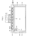
- FIG. 5 is a plan view illustrating a display device according to a second exemplary embodiment of the present invention.
- the display device includes a printed circuit board 100, a display panel 400, and a flexible printed circuit board 530.
- the display panel 400 includes a display substrate 200 and an opposite substrate 300 to be combined with the display substrate 200 to receive a liquid crystal layer (not illustrated).
- the display panel 400 includes a display area DA displaying an image, and first, second and third peripheral areas PA1, PA2 and PA3 surrounding the display area DA.
- a source driving part 520 applying a data signal to a source line DL is mounted on the first peripheral area PA1.
- the source driving part 520 includes first, second, third, fourth, fifth, sixth, seventh and eighth source driving chips LD1, LD2, LD3, LD4, RD1, RD2, RD3 and RD4.
- the first, second, third and fourth source driving chips LD1, LD2, LD3 and LD4 are mounted on a left side of the first peripheral area PA1
- the fifth, sixth, seventh and eighth source driving chips RD1, RD2, RD3 and RD4 are mounted on a right side of the first peripheral area PA1.
- a first signal line part 230, a second signal line part 240 and a connecting line part 250 are formed in the first peripheral area PA1.
- the first signal line part 230 is connected in cascade mode with the first, second, third, fourth, fifth, sixth, seventh and eighth source driving chips LD1, LD2, LD3, LD4, RD1, RD2, RD3 and RD4, to transmit a source driving signal thereto.
- the second signal line part 240 is electrically connected with each of a first gate driving part 620 and a second gate driving part 630, and transmits a gate driving signal thereto.
- the connecting line part 250 electrically connects the neighboring first and second source driving chips LD1 and LD2, and transmits a data signal thereto.
- the source driving signal may include a power voltage VDD and a ground voltage VSS for driving the first, second, third, fourth, fifth, sixth, seventh and eighth source driving chips LD1, LD2, LD3, LD4, RD1, RD2, RD3 and RD4.
- the gate driving signal may include a gate on voltage VON and a gate off voltage VOFF for driving the first and second gate driving parts 620 and 630.
- the first signal line part 230 may have a vertical multiplex structure, for example, having a first line and a second line that are stacked such that the first and second lines are insulated from each other.
- a first signal pad part (not illustrated) electrically connecting the first signal line part 230 with the first driving chip LD1 is formed in the first peripheral area PA1.
- the first signal pad part may have a horizontal multiplex structure that includes a first pad integrally formed with the first line of the first signal line part 230 and a second pad integrally formed with the second line of the first signal line part 230.
- the second signal line part 240 may also have a vertical multiplex structure like in mentioned above.
- a second signal pad part (not illustrated) electrically connecting the second signal line part 240 with the flexible printed circuit board 530 (or a first and a second gate driving parts) may be formed in the horizontal multiplex structure like in mentioned above.
- the first and second gate driving parts 620 and 630 transmitting a gate signal to a gate line GL are formed in the second and third peripheral areas PA2 and PA3, respectively.
- the first and second gate driving parts 620 and 630 are electrically connected with the gate line GL, and transmit a gate signal thereto.
- the first and second gate driving parts 620 and 630 are respectively formed in the second and third peripheral areas PA2 and PA3 that are positioned at each side of the display are DA, but may be formed only in the second peripheral area PA2 in another exemplary embodiment.
- First, second, third, fourth and fifth line parts 531, 532, 533, 534 and 535 electrically connecting the printed circuit board 100 and the display panel 400 are formed at the flexible printed circuit board 530.
- the first line part 531 transmits a source driving signal to the first signal line part 230.
- the source driving signal includes a power voltage and a ground voltage.
- the second line part 532 transmits a data signal to the first, second, third and fourth source driving chips LD1, LD2, LD3 and LD4 mounted on a left side of the first peripheral area PA1.
- the third line part 533 transmits the data signal to the fifth, sixth, seventh and eighth source driving chips RD1, RD2, RD3 and RD4 mounted on a right side of the first peripheral area PA1.
- the fourth line part 534 transmits a gate driving signal to the first gate driving part 620 formed in the second peripheral area PA2, and the fifth line part 535 transmits a gate driving signal to the second gate driving part 630 formed in the third peripheral area PA3.
- FIG. 6 is a partially enlarged plan view illustrating the first peripheral area in FIG. 5.
- the first peripheral area PA1 is sectioned into a mounting area CA and a separating area IA positioned between the neighboring mounting areas CA.
- the source driving chips are mounted on the mounting area CA.
- the first signal line part 230 is formed in the separating area IA.
- a first signal pad part SP1 electrically connecting the first signal line part 230 and the source driving chip is formed on the mounting area CA.
- the first signal line part 230 may be commonly formed in both the mounting area CA and the separating area IA.
- the first signal line part 230 includes a power line 231 transmitting a power voltage VDD and a ground line 233 transmitting a ground voltage VSS.
- the first signal pad part SP1 includes a power pad part 232 electrically connected with the power line 231, and a ground pad part 234 electrically connected with the ground line 233.
- the first signal line part 230 may have a vertical multiplex structure, for example, having a first line and a second line that are stacked such that the first and second lines are insulated from each other.
- the first signal pad part SP1 may have a horizontal multiplex structure that includes a first pad electrically connected with the first line and a second pad electrically connected with the second line.
- the power line 231 includes a first line 231a formed with a first conductive layer and a second line 231 b formed with a second conductive layer.
- the second line 231 b is formed so that the second line 231 b overlaps with the first line 231 a.
- a first pad 232a of the power pad part 232 is integrally formed with the first line 231 a, and a second pad 232b of the power pad part 232 is integrally formed with the second line 231 b.
- the first and second pads 232a and 232b of the power pad part 232 are electrically connected with a conductive pattern 232c formed with a third conductive layer.
- the first and second lines 231 a and 231 b of the power line 231 form a parallelly connected line resistance, so that the line resistance of the power line 231 may be reduced.
- the ground line 233 includes a first line 233a formed with the first conductive layer and a second line 233b formed with the second conductive layer.
- the second line 233b is formed so that the second line 233b overlaps with the first line 233a.
- a first pad 234a of the ground pad part 234 is integrally formed with the first line 233a, and a second pad 234b of the ground pad part 234 is integrally formed with the second line 234b.
- the first and second pads 234a and 234b of the ground pad part 234 are electrically connected with a conductive pattern 234c formed with the third conductive layer.
- the first and second lines 233a and 233b of the ground line 233 form a parallelly connected line resistance, so that the line resistance of the ground line 233 may be reduced.
- FIG. 7 is a partially enlarged plan view illustrating a first peripheral area according to a third exemplary embodiment of the present invention.
- the first peripheral area in FIG. 7 has a substantially same structure as the first peripheral area in FIG. 6 except for a protecting pattern. Therefore, the same reference number will be used to refer to the same parts as those described in FIG. 6, and detailed descriptions of the same elements will be omitted.
- a first signal line part 230 is formed in the first peripheral area PA1.
- the first signal line part 230 includes first lines 231a and 233a formed with a first conductive layer, second lines 231 b and 233b formed with a second conductive layer, and a protecting pattern 235 formed with a third conductive layer.
- the protecting pattern 235 covers the second lines 231 b and 233b formed with the second conductive layer, and formed to be in an electrically floating state.
- a thin passivation layer having a thickness of about 2000 ⁇ (Angstrom, 10 -10 meters) is formed over the second lines 231 b and 233b.
- the thin thickness of the passivation layer causes a pinhole in the air, and the second lines 231 b and 233b may be corroded because of the pinhole.
- the protecting pattern 235 is integrally formed over the power line 231 and the ground line 233, but the protecting pattern may be separately formed to cover the power line 231 and the ground line 233, respectively.
- FIG. 8 is a partially enlarged plan view illustrating a display device according to a fourth exemplary embodiment of the present invention.
- a first peripheral area PA1 of a display panel is sectioned into a mounting area CA and a separating area IA positioned between the neighboring mounting areas CA.
- a source driving chip is mounted in the mounting area CA.
- a connecting line part 250 for transmitting a data signal is formed in the separating area IA.
- a first signal line part 260 and a second signal line part 270 are formed commonly in both the mounting area CA and the separating area IA.
- the first signal line part 260 includes a power line 261 and a ground line 262 that transmit first source driving signals VDD1 and VSS1, respectively.
- the second signal line part 270 includes a power line 271 and a ground line 272 that transmit second source driving signals VDD2 and VSS2, respectively.
- An input pad part IP, an output pad part OP, a first signal pad part SP1 and a second signal pad part SP2 are formed on the mounting area CA.
- the input pad part IP is in contact with an input terminal of the source driving chip
- the output pad part OP is in contact with an output terminal of the source driving chip.
- the first signal pad part SP1 connects the first signal line part 260 with the source driving chip
- the second signal pad part SP2 connects the second signal line part 270 with the source driving chip.
- a fan out part FO is formed in the mounting area CA and the separating area IA. The fan out part FO electrically connects the output pad part OP with a source line DL.
- the first signal line part 260 is extended from a lower portion of the mounting area CA to the separating area IA to cross the fan out part FO.
- the first signal line part 260 and the fan out part FO are formed with conductive layers insulated from each other, and formed to partially overlap. Accordingly, a voltage drop of the driving voltage transmitted via the first signal line part 260 may be prevented. Moreover, a line resistance of the first signal line part 260 may be reduced because another line is formed at another layer over the first signal line part.
- the first signal line part 260 may have a vertical multiplex structure, for example, that includes a first line formed with a first conductive layer and a second line formed with a second conductive layer, where the first line and the second line are insulated from each other and are stacked.
- the fan out part FO is formed with a third conductive layer insulated with the second conductive layer.
- the first signal pad part SP1 may have a horizontal multiplex structure that includes a first pad electrically connected with the first line and a second pad electrically connected with the second line part 260.
- the second signal line part 270 is extended from an upper portion of the mounting area CA to the separating area IA.
- the second signal line part 270 and the connecting line part 250 are formed with conductive layers insulated from each other, and formed to partially overlap.
- the second signal line part 270 may have a vertical multiplex structure, for example, where the first line and the second line are stacked. The first line is formed with the first conductive layer and the second line is formed with the second conductive layer. The connecting line part 250 is formed with the third conductive layer.
- the second signal pad part SP2 may have a horizontal multiplex structure that includes a first pad electrically connected with the first line and a second pad electrically connected with the second line.
- the first portion when the first signal line part 260 is sectioned into a first portion overlapped with the fan out part FO and a second portion not overlapped with the fan out part FO, the first portion may be formed in a single-layer structure, and the second portion may be formed in a multi-layer structure so that the first and second lines are stacked.
- the first signal line part 270 when the first signal line part 270 is sectioned into a third portion overlapped with the connecting line part 250 and a fourth portion not overlapped with the connecting line part 250, the third portion may be formed in a single-layer structure, and the fourth portion may be formed in a multi-layer structure where the first and second lines are stacked.
- the first and third portions are formed with the first conductive layer, and the second and the fourth portions are formed with the second conductive layer.
- the fan out part FO and the connecting line part 250 are formed with the second conductive layer.
- the first conductive layer is a gate metal layer
- the second conductive layer is a source metal layer
- the third conductive layer is a pixel electrode layer.
- FIG. 9 is an enlarged plan view illustrating the first signal line part and the first signal pad part in FIG. 8.
- FIG. 10 is a partial cross-sectional view taken along a line III-III' in FIG. 9.
- the signal line part 260 includes the power line 261 and the ground line 262.
- the first signal pad part SP1 includes a power pad part (not illustrated) electrically connected with the power line 261, and a ground pad part 263 electrically connected with the ground line 262.
- An output line OL of the fan out part FO is formed over the ground line 262 to cross each other.
- the output line OL is electrically connected with the source line DL.
- a first line 262a of the ground line 262 and a first pad 263a of the ground pad part 263 are formed on a base substrate 201.
- the first line 262a is formed with a first conductive layer.
- the first pad 263a is integrally formed with the first line 262a.
- the first conductive layer may be a gate metal layer forming the gate line GL and a gate electrode of a switching element TFT.
- a gate insulating layer 202 is formed over the first line 262a and the first pad 263a.
- a second line 262b of the ground line 262 is formed over the gate insulating layer 202 with a second conductive layer so that the second line 262b overlaps with the first line 262a.
- a second pad 263b of the ground pad part 263 is integrally formed with the second line 262b.
- the second conductive layer may be a source metal layer forming the source line DL, a source electrode and a drain electrode of the switching element TFT.
- a passivation layer 203 is formed over the second line 262b and the second pad 263b.
- a contact hole exposing the first and second pads 263a and 263b is formed at the passivation layer 203.
- a conductive pattern 263c electrically connected with the first and second pads 263a and 263b via the contact hole is formed at the passivation layer 203.
- the conductive pattern 263c is formed with a third conductive layer
- the output line OL is formed with the third conductive layer over the ground line 262. An end portion of the output line OL is electrically connected with the source line DL via the contact hole.
- the third conductive layer may be a transparent conductive layer forming a pixel electrode of the liquid crystal capacitor CLC electrically connected with the switching element TFT.
- the first line 262a receives a ground voltage VSS1 through the first pad 263a
- the second line 262b receives the ground voltage VSS1 through the second pad 263b. Consequently, the ground line 262 has a parallel line resistance because the first line 262a and the second line 262b are formed in parallel with each other. Therefore, the line resistance of the ground line 262 may be reduced.
- a surplus space of the display panel may be efficiently utilized.
- a signal line part directly formed on a display panel has a multiplex structure where a first line and a second line are insulated from each other and are stacked, so that a line resistance may be reduced.
- the signal line part is electrically connected with a signal pad part applying a driving signal thereto.
- the signal pad part includes a first pad applying the driving signal to the first line, and a second pad applying the driving signal to the second line. Accordingly, a first resistance caused by the first line and a second resistance caused by the second line forms a parallelly connected line resistance, so that the line resistance of the signal line part may be reduced.
- another line is formed at another layer over the first signal line part to overlap with each other, so that the line resistance of the signal line part may be minimized and a space of the display panel where lines are to be formed may be more efficiently utilized.
Landscapes
- Physics & Mathematics (AREA)
- Nonlinear Science (AREA)
- Mathematical Physics (AREA)
- Chemical & Material Sciences (AREA)
- Crystallography & Structural Chemistry (AREA)
- General Physics & Mathematics (AREA)
- Optics & Photonics (AREA)
- Devices For Indicating Variable Information By Combining Individual Elements (AREA)
- Liquid Crystal (AREA)
Abstract
Description
- This application relies for priority upon Patent Application No.
2006-60481 filed in the Korean Intellectual Property Office, Republic of Korea, on June 30, 2006 - Embodiments of the present invention relate to a display substrate and a display device having the display substrate. More particularly, embodiments of the present invention relate to a display substrate and a display device having the display substrate providing a reduced line resistance.
- Generally, a liquid crystal display device includes a display panel for displaying an image by using an optical transmittance of a liquid crystal, and a gate driving circuit and a source driving circuit that are electrically connected with the display panel. The display panel includes a plurality of pixel parts. Each of the pixel parts includes a switching element and a liquid crystal capacitor electrically connected with the switching element. The gate driving circuit outputs a gate signal to turn on the switching element. The source driving circuit outputs a data signal to drive the liquid crystal capacitor.
- A gate driving circuit and a source driving circuit formed as a chip may be directly mounted on the display panel for manufacturing a lighter, thinner, shorter, and smaller liquid crystal display device. In a chip on glass structure as mentioned above, signal lines transmitting driving signals to the chip are formed directly on the display panel. When the signal lines are formed directly on the display panel, a signal delay may be induced due to a line resistance of the signal lines, where the signal delay degrades the display quality.
- In accordance with one or more embodiment of the present invention, a display substrate capable of reducing a line resistance is provided. A display device having the display substrate is also provided. More particularly, in a display substrate according to an exemplary embodiment, the display substrate includes a plurality of pixel parts, a signal line part and a signal pad part. The pixel parts are formed in a display area. The signal line part is formed in a peripheral area surrounding the display area. The signal line part includes a first line formed with a first conductive layer, and a second line formed with a second conductive layer over the first line. The second line overlaps the first line. The signal pad part includes a first pad integrally formed with the first line, and a second pad integrally formed with the second line.
- In a display device according to another exemplary embodiment of the present invention, the display device includes a plurality of pixel parts, a signal line part and a signal pad part. The pixel parts are formed in a display area. The signal line part is formed in a peripheral area surrounding the display area. The signal line part includes a first line formed with a first conductive layer, and a second line formed with a second conductive layer over the first line. The second line overlaps the first line. The signal pad part includes a first pad integrally formed with the first line, and a second pad integrally formed with the second line. According to the above mentioned display substrate and display device having the display substrate, a line resistance of a signal line part may be reduced because the signal line part includes a first line and a second line that are insulated from each other and are stacked.
- The scope of the present invention is defined by the claims, which are incorporated into this section by reference. A more complete understanding of embodiments of the present invention will be afforded to those skilled in the art, as well as a realization of additional advantages thereof, by a consideration of the following detailed description. Reference will be made to the appended sheets of drawings that will first be described briefly.
- The above and other features and advantages of the present invention will become more apparent by describing, in detail, exemplary embodiments thereof with reference to the accompanying drawings, in which:
- FIG. 1 is a plan view illustrating a display device according to a first exemplary embodiment of the present invention;
- FIG. 2A is a partially enlarged plan view illustrating the first peripheral area in FIG. 1;
- FIG. 2B is a partially enlarged plan view illustrating the second peripheral area in FIG. 1;
- FIG. 3 is an enlarged plan view illustrating the second signal line part and the second signal pad part in FIG. 2B;
- FIG. 4 is a partial cross-sectional view taken along a line I-I' and a line II-II' in FIG. 3;
- FIG. 5 is a plan view illustrating a display device according to a second exemplary embodiment of the present invention;
- FIG. 6 is a partially enlarged plan view illustrating the first peripheral area in FIG. 5;
- FIG. 7 is a partially enlarged plan view illustrating a first peripheral area according to a third exemplary embodiment of the present invention;
- FIG. 8 is a partially enlarged plan view illustrating a display device according to a fourth exemplary embodiment of the present invention;
- FIG. 9 is an enlarged plan view illustrating the first signal line part and the first signal pad part in FIG. 8; and
- FIG. 10 is a partial cross-sectional view taken along a line III-III' in FIG. 9.
- Embodiments of the present invention and their advantages are best understood by referring to the detailed description that follows. It should be appreciated that like reference numerals are used to identify like elements illustrated in one or more of the figures.
- The present invention now will be described more fully hereinafter with reference to the accompanying drawings, in which embodiments of the invention are shown. This invention may, however, be embodied in many different forms and should not be construed as limited to the embodiments set forth herein; rather, these embodiments are provided so that this disclosure will be thorough and complete, and will fully convey the scope of the invention to those skilled in the art. It will be understood that when an element is referred to as being "on" or "onto" another element, it may be directly on the other element or intervening elements may also be present. In contrast, when an element is referred to as being "directly on" another element, there are no intervening elements present. In the drawings, the thickness of layers, films, panels, regions, etc., may be exaggerated for clarity. Like reference numerals refer to similar or identical elements throughout.
- FIG. 1 is a plan view illustrating a display device according to a first exemplary embodiment of the present invention. Referring to FIG. 1, the display device includes a printed
circuit board 100, adisplay panel 400, asource driving part 510, and agate driving part 610. Amain driving circuit 110 is mounted on the printedcircuit board 100. The printedcircuit board 100 is electrically connected with thedisplay panel 400 through thesource driving part 510. Thesource driving part 510 includes first, second, third, fourth, fifth, sixth, seventh and eighth sourcetape carrier packages gate driving part 610 includes first, second and third gate tape carrier packages 611, 612 and 613. The tape carrier package (hereinafter, 'TCP') is a flexible printed circuit board on which a driving chip is mounted. A plurality ofline parts main driving circuit 110 to thedisplay panel 400, are formed on the printedcircuit board 100. For example, afirst line part 120 transmits a source driving signal to thesource driving part 510. Asecond line part 131 transmits a data signal to the first, second, third andfourth source TCPs display panel 400. Athird line part 132 transmits a data signal to the fifth, sixth, seventh andeighth source TCPs display panel 400. Thefourth line part 140 transmits a gate driving signal to the first, second andthird gate TCPs - The
display panel 400 includes adisplay substrate 200 and anopposite substrate 300 to be combined with thedisplay substrate 200 to receive a liquid crystal layer (not illustrated). Thedisplay panel 400 includes a display area DA displaying an image, and first and second peripheral areas PA1 and PA2 surrounding the display area DA. A plurality of source lines DL and a plurality of gate lines GL crossing the source lines DL are formed in the display area DA. The source lines DL and the gate lines GL define a plurality of pixel parts 'P'. A switching element TFT, a liquid crystal capacitor CLC and a storage capacitor CST are formed in each of the pixel parts 'P'. - The
source driving part 510 is mounted in the first peripheral area PA1. For example, the first, second, third andfourth source TCPs eighth source TCPs signal line part 210 applying a source driving signal to thesource driving part 510 is formed in the first peripheral area PA1. The firstsignal line part 210 is formed between the neighboring source TCPs. The firstsignal line part 210 transmits the source driving signal to the first, second, third, fourth, fifth, sixth, seventh and eighth source tape carrier packages 511, 512, 513, 514, 515, 516, 517 and 518 in a cascade mode. The source driving signal may be a driving voltage VDD or VSS for driving a source driving chip mounted on the source TCP. The firstsignal line part 210 may include a power line and a ground line. The firstsignal line part 210 may include stacked metal layers that are insulated from each other. - The
gate driving part 610 is mounted on the second peripheral area PA2. For example, the first, second andthird gate TCPs signal line part 220, which transmits a gate driving signal to the first, second andthird gate TCPs signal line part 220 is formed between the neighboring source TCPs. The secondsignal line part 220 transmits the gate driving signal to the first, second andthird gate TCPs signal line part 220 may include a power line and a ground line. The secondsignal line part 220 may include stacked metal layers that are insulated from each other. - FIG. 2A is a partially enlarged plan view illustrating the first peripheral area in FIG. 1. FIG. 2B is a partially enlarged plan view illustrating the second peripheral area in FIG. 1. Referring to FIGS. 1 and 2A, the first peripheral area PA1 is sectioned into a first mounting area CA1 and a first separating area IA1 positioned between the neighboring first mounting areas CA1. The source TCPs are mounted on the first mounting area CA1. A first input-output pad part IOP1 electrically connected with input-output terminals of the source TCPs is formed in the first mounting area CA1. The first
signal line part 210 for transmitting the source driving signal in a cascade mode is formed in the first separating area IA1. - The first input-output pad part IOP1 includes a source pad part DP and a first signal pad part SP1. The source pad part DP is electrically connected with a first fan out part F01 and applies the data signal to the source lines DL. The first signal pad part SP1 is electrically connected with the first
signal line part 210. The firstsignal line part 210 includes apower line 211 transmitting a power voltage VDD and aground line 213 transmitting a ground voltage VSS. The firstsignal line part 210 may have a vertical multiplex or interleaved structure, for example, having a first line and a second line that are stacked such that the first and second lines are insulated from each other. The first signal pad part SP1 may have a horizontal multiplex structure that includes a first pad integrally formed with the first line and a second pad integrally formed with the second line. - Referring to FIGS. 1 and 2B, the second peripheral area PA2 is sectioned into a second mounting area CA2 and a second separating area IA2. The gate TCPs are mounted on the second mounting area CA2. A second input-output pad part IOP2 electrically connected with input-output terminals of the gate TCPs is formed in the second mounting area CA2. The second
signal line part 220 for transmitting the gate driving signal in a cascade mode is formed in the second separating area IA2. The second input-output pad part IOP2 includes a gate pad part GP and a second signal pad part SP2. The gate pad part GP is electrically connected with a second fan out part FO2 and applies the gate signal to the gate lines GL. The second signal pad part SP2 is electrically connected with the secondsignal line part 220. The secondsignal line part 220 includes apower line 221 transmitting a gate on voltage VON and aground line 223 transmitting a gate off voltage VOFF. The gatesignal line part 220 may have a vertical multiplex structure, for example, having a first line and a second line that are stacked such that the first and second lines are insulated from each other. The second signal pad part SP2 may have a horizontal multiplex structure that includes a first pad integrally formed with the first line and a second pad integrally formed with the second line. - Referring to FIGS. 2A and 2B, the first and second
signal line parts signal line parts signal line part 220 and the second signal pad part SP2. - FIG. 3 is an enlarged plan view illustrating the second signal line part and the second signal pad part in FIG. 2B. FIG. 4 is a partial cross-sectional view taken along a line I-I' and a line II-II' in FIG. 3. Referring to FIGS. 3 and 4, the signal line part includes the
power line 221 and theground line 223. The second signal line part includes apower pad part 222 formed at an end portion of thepower line 221, and aground pad part 224 formed at an end portion of theground line 223. For example, afirst line 221 a of thepower line 221 and afirst pad 222a of thepower pad part 222 are formed on abase substrate 201. Thefirst pad 222a of thepower pad part 222 is formed at an end portion of thefirst line 221 a. Thefirst line 221 a and thefirst pad 222a are formed with a first conductive layer. The first conductive layer may be a gate metal layer forming the gate line GL and a gate electrode of the switching element TFT connected with the gate line GL. - A
gate insulating layer 202 is formed over thefirst line 221 a and thefirst pad 222a. Asecond line 221 b of thepower line 221 is formed over thegate insulating layer 202 so that thesecond line 221 b overlaps with thefirst line 221 a. Asecond pad 222b of thepower pad part 222 is formed at an end portion of thesecond line 221 b. Thesecond line 221 b and thesecond pad 222b are formed with a second conductive layer. The second conductive layer may be a source metal layer forming the source line DL, a source electrode and a drain electrode of the switching element TFT. Apassivation layer 203 is formed over thesecond line 221 b and thesecond pad 222b. A contact hole exposing the first andsecond pads passivation layer 203. Aconductive pattern 222c electrically connected with the first andsecond pads passivation layer 203. Theconductive pattern 222c is formed with a third conductive layer. The third conductive layer may be a transparent conductive layer forming a pixel electrode of the liquid crystal capacitor CLC electrically connected with the switching element TFT. Thefirst line 221 a receives the gate on voltage VON through thefirst pad 222a, and thesecond line 221 b receives the gate on voltage VON through thesecond pad 222b. Thepower line 221 has a parallel connection resistance because thefirst line 221 a and thesecond line 221b are formed in parallel with each other. Therefore, the line resistance of thepower line 221 may be reduced. - FIG. 5 is a plan view illustrating a display device according to a second exemplary embodiment of the present invention. Referring to FIG. 5, the display device includes a printed
circuit board 100, adisplay panel 400, and a flexible printedcircuit board 530. Thedisplay panel 400 includes adisplay substrate 200 and anopposite substrate 300 to be combined with thedisplay substrate 200 to receive a liquid crystal layer (not illustrated). Thedisplay panel 400 includes a display area DA displaying an image, and first, second and third peripheral areas PA1, PA2 and PA3 surrounding the display area DA. Asource driving part 520 applying a data signal to a source line DL is mounted on the first peripheral area PA1. Thesource driving part 520 includes first, second, third, fourth, fifth, sixth, seventh and eighth source driving chips LD1, LD2, LD3, LD4, RD1, RD2, RD3 and RD4. For example, the first, second, third and fourth source driving chips LD1, LD2, LD3 and LD4 are mounted on a left side of the first peripheral area PA1, and the fifth, sixth, seventh and eighth source driving chips RD1, RD2, RD3 and RD4 are mounted on a right side of the first peripheral area PA1. - A first
signal line part 230, a secondsignal line part 240 and a connectingline part 250 are formed in the first peripheral area PA1. The firstsignal line part 230 is connected in cascade mode with the first, second, third, fourth, fifth, sixth, seventh and eighth source driving chips LD1, LD2, LD3, LD4, RD1, RD2, RD3 and RD4, to transmit a source driving signal thereto. The secondsignal line part 240 is electrically connected with each of a firstgate driving part 620 and a secondgate driving part 630, and transmits a gate driving signal thereto. The connectingline part 250 electrically connects the neighboring first and second source driving chips LD1 and LD2, and transmits a data signal thereto. The source driving signal may include a power voltage VDD and a ground voltage VSS for driving the first, second, third, fourth, fifth, sixth, seventh and eighth source driving chips LD1, LD2, LD3, LD4, RD1, RD2, RD3 and RD4. The gate driving signal may include a gate on voltage VON and a gate off voltage VOFF for driving the first and secondgate driving parts signal line part 230 may have a vertical multiplex structure, for example, having a first line and a second line that are stacked such that the first and second lines are insulated from each other. A first signal pad part (not illustrated) electrically connecting the firstsignal line part 230 with the first driving chip LD1 is formed in the first peripheral area PA1. The first signal pad part may have a horizontal multiplex structure that includes a first pad integrally formed with the first line of the firstsignal line part 230 and a second pad integrally formed with the second line of the firstsignal line part 230. - The second
signal line part 240 may also have a vertical multiplex structure like in mentioned above. A second signal pad part (not illustrated) electrically connecting the secondsignal line part 240 with the flexible printed circuit board 530 (or a first and a second gate driving parts) may be formed in the horizontal multiplex structure like in mentioned above. The first and secondgate driving parts gate driving parts gate driving parts - First, second, third, fourth and
fifth line parts circuit board 100 and thedisplay panel 400 are formed at the flexible printedcircuit board 530. For example, thefirst line part 531 transmits a source driving signal to the firstsignal line part 230. The source driving signal includes a power voltage and a ground voltage. Thesecond line part 532 transmits a data signal to the first, second, third and fourth source driving chips LD1, LD2, LD3 and LD4 mounted on a left side of the first peripheral area PA1. Thethird line part 533 transmits the data signal to the fifth, sixth, seventh and eighth source driving chips RD1, RD2, RD3 and RD4 mounted on a right side of the first peripheral area PA1. Thefourth line part 534 transmits a gate driving signal to the firstgate driving part 620 formed in the second peripheral area PA2, and thefifth line part 535 transmits a gate driving signal to the secondgate driving part 630 formed in the third peripheral area PA3. - FIG. 6 is a partially enlarged plan view illustrating the first peripheral area in FIG. 5. Referring to FIGS. 5 and 6, the first peripheral area PA1 is sectioned into a mounting area CA and a separating area IA positioned between the neighboring mounting areas CA. The source driving chips are mounted on the mounting area CA. The first
signal line part 230 is formed in the separating area IA. A first signal pad part SP1 electrically connecting the firstsignal line part 230 and the source driving chip is formed on the mounting area CA. The firstsignal line part 230 may be commonly formed in both the mounting area CA and the separating area IA. - The first
signal line part 230 includes apower line 231 transmitting a power voltage VDD and aground line 233 transmitting a ground voltage VSS. The first signal pad part SP1 includes apower pad part 232 electrically connected with thepower line 231, and aground pad part 234 electrically connected with theground line 233. The firstsignal line part 230 may have a vertical multiplex structure, for example, having a first line and a second line that are stacked such that the first and second lines are insulated from each other. The first signal pad part SP1 may have a horizontal multiplex structure that includes a first pad electrically connected with the first line and a second pad electrically connected with the second line. Thepower line 231 includes afirst line 231a formed with a first conductive layer and asecond line 231 b formed with a second conductive layer. Thesecond line 231 b is formed so that thesecond line 231 b overlaps with thefirst line 231 a. Afirst pad 232a of thepower pad part 232 is integrally formed with thefirst line 231 a, and asecond pad 232b of thepower pad part 232 is integrally formed with thesecond line 231 b. The first andsecond pads power pad part 232 are electrically connected with aconductive pattern 232c formed with a third conductive layer. The first andsecond lines power line 231 form a parallelly connected line resistance, so that the line resistance of thepower line 231 may be reduced. - The
ground line 233 includes afirst line 233a formed with the first conductive layer and asecond line 233b formed with the second conductive layer. Thesecond line 233b is formed so that thesecond line 233b overlaps with thefirst line 233a. Afirst pad 234a of theground pad part 234 is integrally formed with thefirst line 233a, and asecond pad 234b of theground pad part 234 is integrally formed with thesecond line 234b. The first andsecond pads ground pad part 234 are electrically connected with aconductive pattern 234c formed with the third conductive layer. The first andsecond lines ground line 233 form a parallelly connected line resistance, so that the line resistance of theground line 233 may be reduced. - FIG. 7 is a partially enlarged plan view illustrating a first peripheral area according to a third exemplary embodiment of the present invention. The first peripheral area in FIG. 7 has a substantially same structure as the first peripheral area in FIG. 6 except for a protecting pattern. Therefore, the same reference number will be used to refer to the same parts as those described in FIG. 6, and detailed descriptions of the same elements will be omitted. Referring to FIGS. 6 and 7, a first
signal line part 230 is formed in the first peripheral area PA1. The firstsignal line part 230 includesfirst lines second lines pattern 235 formed with a third conductive layer. The protectingpattern 235 covers thesecond lines second lines second lines pattern 235 to cover thesecond lines signal line part 230 may be improved. In FIG. 7, the protectingpattern 235 is integrally formed over thepower line 231 and theground line 233, but the protecting pattern may be separately formed to cover thepower line 231 and theground line 233, respectively. - FIG. 8 is a partially enlarged plan view illustrating a display device according to a fourth exemplary embodiment of the present invention. Referring to FIGS. 5 and 8, a first peripheral area PA1 of a display panel is sectioned into a mounting area CA and a separating area IA positioned between the neighboring mounting areas CA. A source driving chip is mounted in the mounting area CA. A connecting
line part 250 for transmitting a data signal is formed in the separating area IA. A firstsignal line part 260 and a secondsignal line part 270 are formed commonly in both the mounting area CA and the separating area IA. The firstsignal line part 260 includes apower line 261 and aground line 262 that transmit first source driving signals VDD1 and VSS1, respectively. The secondsignal line part 270 includes apower line 271 and aground line 272 that transmit second source driving signals VDD2 and VSS2, respectively. - An input pad part IP, an output pad part OP, a first signal pad part SP1 and a second signal pad part SP2 are formed on the mounting area CA. The input pad part IP is in contact with an input terminal of the source driving chip, and the output pad part OP is in contact with an output terminal of the source driving chip. The first signal pad part SP1 connects the first
signal line part 260 with the source driving chip, and the second signal pad part SP2 connects the secondsignal line part 270 with the source driving chip. A fan out part FO is formed in the mounting area CA and the separating area IA. The fan out part FO electrically connects the output pad part OP with a source line DL. The firstsignal line part 260 is extended from a lower portion of the mounting area CA to the separating area IA to cross the fan out part FO. The firstsignal line part 260 and the fan out part FO are formed with conductive layers insulated from each other, and formed to partially overlap. Accordingly, a voltage drop of the driving voltage transmitted via the firstsignal line part 260 may be prevented. Moreover, a line resistance of the firstsignal line part 260 may be reduced because another line is formed at another layer over the first signal line part. - The first
signal line part 260 may have a vertical multiplex structure, for example, that includes a first line formed with a first conductive layer and a second line formed with a second conductive layer, where the first line and the second line are insulated from each other and are stacked. The fan out part FO is formed with a third conductive layer insulated with the second conductive layer. The first signal pad part SP1 may have a horizontal multiplex structure that includes a first pad electrically connected with the first line and a second pad electrically connected with thesecond line part 260. The secondsignal line part 270 is extended from an upper portion of the mounting area CA to the separating area IA. The secondsignal line part 270 and the connectingline part 250 are formed with conductive layers insulated from each other, and formed to partially overlap. Accordingly, a voltage drop of the driving voltage transmitted via the secondsignal line part 270 may be prevented. Moreover, a line resistance of the secondsignal line part 270 may be reduced because another line is formed at another layer over the secondsignal line part 270. The secondsignal line part 270 may have a vertical multiplex structure, for example, where the first line and the second line are stacked. The first line is formed with the first conductive layer and the second line is formed with the second conductive layer. The connectingline part 250 is formed with the third conductive layer. The second signal pad part SP2 may have a horizontal multiplex structure that includes a first pad electrically connected with the first line and a second pad electrically connected with the second line. - In another exemplary embodiment, when the first
signal line part 260 is sectioned into a first portion overlapped with the fan out part FO and a second portion not overlapped with the fan out part FO, the first portion may be formed in a single-layer structure, and the second portion may be formed in a multi-layer structure so that the first and second lines are stacked. Likewise, when the firstsignal line part 270 is sectioned into a third portion overlapped with the connectingline part 250 and a fourth portion not overlapped with the connectingline part 250, the third portion may be formed in a single-layer structure, and the fourth portion may be formed in a multi-layer structure where the first and second lines are stacked. The first and third portions are formed with the first conductive layer, and the second and the fourth portions are formed with the second conductive layer. The fan out part FO and the connectingline part 250 are formed with the second conductive layer. For example, the first conductive layer is a gate metal layer, the second conductive layer is a source metal layer, and the third conductive layer is a pixel electrode layer. - FIG. 9 is an enlarged plan view illustrating the first signal line part and the first signal pad part in FIG. 8. FIG. 10 is a partial cross-sectional view taken along a line III-III' in FIG. 9. Referring to FIGS. 8 to 10, the
signal line part 260 includes thepower line 261 and theground line 262. The first signal pad part SP1 includes a power pad part (not illustrated) electrically connected with thepower line 261, and aground pad part 263 electrically connected with theground line 262. An output line OL of the fan out part FO is formed over theground line 262 to cross each other. The output line OL is electrically connected with the source line DL. For example, afirst line 262a of theground line 262 and afirst pad 263a of theground pad part 263 are formed on abase substrate 201. Thefirst line 262a is formed with a first conductive layer. Thefirst pad 263a is integrally formed with thefirst line 262a. The first conductive layer may be a gate metal layer forming the gate line GL and a gate electrode of a switching element TFT. - A
gate insulating layer 202 is formed over thefirst line 262a and thefirst pad 263a. Asecond line 262b of theground line 262 is formed over thegate insulating layer 202 with a second conductive layer so that thesecond line 262b overlaps with thefirst line 262a. Asecond pad 263b of theground pad part 263 is integrally formed with thesecond line 262b. The second conductive layer may be a source metal layer forming the source line DL, a source electrode and a drain electrode of the switching element TFT. Apassivation layer 203 is formed over thesecond line 262b and thesecond pad 263b. A contact hole exposing the first andsecond pads passivation layer 203. Aconductive pattern 263c electrically connected with the first andsecond pads passivation layer 203. Theconductive pattern 263c is formed with a third conductive layer. - The output line OL is formed with the third conductive layer over the
ground line 262. An end portion of the output line OL is electrically connected with the source line DL via the contact hole. The third conductive layer may be a transparent conductive layer forming a pixel electrode of the liquid crystal capacitor CLC electrically connected with the switching element TFT. Thefirst line 262a receives a ground voltage VSS1 through thefirst pad 263a, and thesecond line 262b receives the ground voltage VSS1 through thesecond pad 263b. Consequently, theground line 262 has a parallel line resistance because thefirst line 262a and thesecond line 262b are formed in parallel with each other. Therefore, the line resistance of theground line 262 may be reduced. Moreover, through forming theground line 262 and the fan out part FO to overlap with each other, a surplus space of the display panel may be efficiently utilized. - According to an embodiment of the present invention as mentioned above, a signal line part directly formed on a display panel has a multiplex structure where a first line and a second line are insulated from each other and are stacked, so that a line resistance may be reduced. The signal line part is electrically connected with a signal pad part applying a driving signal thereto. The signal pad part includes a first pad applying the driving signal to the first line, and a second pad applying the driving signal to the second line. Accordingly, a first resistance caused by the first line and a second resistance caused by the second line forms a parallelly connected line resistance, so that the line resistance of the signal line part may be reduced. Moreover, another line is formed at another layer over the first signal line part to overlap with each other, so that the line resistance of the signal line part may be minimized and a space of the display panel where lines are to be formed may be more efficiently utilized.
- Although exemplary embodiments of the present invention have been described, it is understood that the present invention should not be limited to these exemplary embodiments but various changes and modifications can be made by one ordinary skilled in the art within the spirit and scope of the present invention as hereinafter claimed.
Claims (17)
- A display substrate, comprising:a plurality of pixel parts formed in a display area;a signal line part formed in a peripheral area surrounding the display area, the signal line part including:a first line formed with a first conductive layer; anda second line formed with a second conductive layer over the first line, the second line overlapping the first line; anda signal pad part including:a first pad integrally formed with the first line; anda second pad integrally formed with the second line.
- The display substrate of claim 1, further comprising a protecting pattern formed with a third conductive layer to cover the second line.
- A display device, comprising:a plurality of pixel parts formed in a display area;a signal line part formed in a peripheral area surrounding the display area, the signal line part including:a first line formed with a first conductive layer; anda second line formed with a second conductive layer over the first line, the second line overlapping the first line; anda signal pad part including:a first pad integrally formed with the first line; anda second pad integrally formed with the second line.
- The display device of claim 3, wherein the signal pad part further includes a conductive pattern electrically connected with the first pad and the second pad, and the conductive pattern is formed with a third conductive layer.
- The display device of claim 4, further comprising a protecting pattern formed with the third conductive layer to cover the second line.
- The display device of claim 4, further comprising:a gate line electrically connected with the pixel parts, the gate line formed with the first conductive layer in the display area; anda gate driving part outputting a gate signal to the gate line, the gate driving part formed in the peripheral area.
- The display device of claim 6, wherein the signal line part transmits a gate driving signal for driving the gate driving part.
- The display device of claim 6, wherein the gate driving part is a gate tape carrier package on which a gate driving chip producing the gate signal is mounted.
- The display device of claim 4, further comprising:a source line electrically connected with the pixel parts, the source line formed with the second conductive layer in the display area; anda source driving part outputting a data signal to the source line, the source driving part formed in the peripheral area.
- The display device of claim 9, wherein the signal line part transmits a source driving signal for driving the source driving part.
- The display device of claim 9, wherein the source driving part is a source tape carrier package on which a source driving chip producing the data signal is mounted.
- The display device of claim 9, further comprising:an output pad part electrically connected with an output terminal of the source driving part;a fan out part electrically connecting the output pad part with the source line;an input pad part electrically connected with an input terminal of the source driving part; anda connecting line part electrically connected with the input pad part, the connecting line part formed in the peripheral area.
- The display device of claim 12, wherein the signal line part includes a first signal line part partially overlapped with the fan out part, and a second signal line part partially overlapped with the connecting line part.
- The display device of claim 13, wherein the fan out part and the connecting line part are formed with the third conductive layer.
- The display device of claim 13, wherein the first signal line part is sectioned into a first portion overlapped with the fan out part and a second portion not overlapped with the fan out part,
wherein the first portion is formed with the first line, and the second portion has a multiplex structure such that the first line and second line are stacked. - The display device of claim 15, wherein the second signal line part is sectioned into a third portion overlapped with the connecting line part and a fourth portion not overlapped with the connecting line part,
wherein the third portion is formed with the first line, and the fourth portion has a multiplex structure such that the first line and second line are stacked. - The display device of claim 16, wherein the fan out part and the connecting line part are formed with the second conductive layer.
Applications Claiming Priority (1)
| Application Number | Priority Date | Filing Date | Title |
|---|---|---|---|
| KR1020060060481A KR20080001975A (en) | 2006-06-30 | 2006-06-30 | Display substrate and display device having same |
Publications (2)
| Publication Number | Publication Date |
|---|---|
| EP1873581A2 true EP1873581A2 (en) | 2008-01-02 |
| EP1873581A3 EP1873581A3 (en) | 2009-10-07 |
Family
ID=38663083
Family Applications (1)
| Application Number | Title | Priority Date | Filing Date |
|---|---|---|---|
| EP07011550A Withdrawn EP1873581A3 (en) | 2006-06-30 | 2007-06-13 | Display substrate and display device having the same |
Country Status (5)
| Country | Link |
|---|---|
| US (1) | US8049856B2 (en) |
| EP (1) | EP1873581A3 (en) |
| JP (1) | JP2008015507A (en) |
| KR (1) | KR20080001975A (en) |
| CN (1) | CN101097324A (en) |
Cited By (1)
| Publication number | Priority date | Publication date | Assignee | Title |
|---|---|---|---|---|
| CN114334690A (en) * | 2021-12-27 | 2022-04-12 | 武汉天马微电子有限公司 | Display panel and display device |
Families Citing this family (30)
| Publication number | Priority date | Publication date | Assignee | Title |
|---|---|---|---|---|
| KR101082893B1 (en) * | 2005-08-24 | 2011-11-11 | 삼성전자주식회사 | Array substrate and display apparatus hving the same |
| KR20110062170A (en) * | 2009-12-02 | 2011-06-10 | 엘지디스플레이 주식회사 | LCD Display |
| WO2011087168A1 (en) * | 2010-01-15 | 2011-07-21 | 삼성엘이디 주식회사 | Printed circuit board |
| KR101258260B1 (en) * | 2010-04-16 | 2013-04-25 | 엘지디스플레이 주식회사 | Organic Light Emitting Display Device |
| KR101696393B1 (en) | 2010-06-15 | 2017-01-16 | 삼성디스플레이 주식회사 | Display panel |
| KR101324383B1 (en) * | 2010-10-25 | 2013-11-01 | 엘지디스플레이 주식회사 | Liquid crystal display |
| CN102253507B (en) * | 2011-04-08 | 2014-03-26 | 深圳市华星光电技术有限公司 | Chip fanout forming method |
| KR101871773B1 (en) * | 2012-07-25 | 2018-06-27 | 엘지디스플레이 주식회사 | Plastic panel and flat panel display device using the same |
| KR101876234B1 (en) * | 2012-07-25 | 2018-07-09 | 엘지디스플레이 주식회사 | Plastic panel and flat panel display device using the same |
| CN103489879B (en) * | 2013-10-11 | 2016-04-20 | 京东方科技集团股份有限公司 | Array base palte and preparation method thereof, display unit |
| KR102279058B1 (en) * | 2014-07-25 | 2021-07-20 | 삼성디스플레이 주식회사 | Display apparatus |
| CN104142588B (en) * | 2014-07-30 | 2017-01-25 | 深圳市华星光电技术有限公司 | Liquid crystal display panel and liquid crystal display |
| KR102194484B1 (en) * | 2014-09-05 | 2020-12-24 | 엘지디스플레이 주식회사 | Drive Printed-Circuit Board for Display Device and Display Device having the same |
| TWI504969B (en) * | 2014-10-27 | 2015-10-21 | Au Optronics Corp | Display panel and display device |
| CN107004386B (en) * | 2014-11-21 | 2019-10-15 | 夏普株式会社 | display device |
| CN105390114B (en) * | 2015-12-15 | 2017-12-22 | 武汉华星光电技术有限公司 | Liquid crystal display device |
| JP2017181594A (en) * | 2016-03-28 | 2017-10-05 | パナソニック液晶ディスプレイ株式会社 | Display device |
| KR102539031B1 (en) * | 2016-04-28 | 2023-06-02 | 삼성디스플레이 주식회사 | Display device |
| CN105976748A (en) * | 2016-07-01 | 2016-09-28 | 武汉华星光电技术有限公司 | Display panel driving device and display device |
| CN106125418A (en) * | 2016-08-11 | 2016-11-16 | 深圳市华星光电技术有限公司 | Display device and display floater thereof |
| CN106531119A (en) * | 2017-01-10 | 2017-03-22 | 深圳市华星光电技术有限公司 | Drive circuit and display device |
| CN108845465B (en) * | 2018-07-02 | 2020-07-28 | 深圳市华星光电半导体显示技术有限公司 | Fan-out wiring structure of display panel and manufacturing method thereof |
| CN208422916U (en) | 2018-08-07 | 2019-01-22 | 京东方科技集团股份有限公司 | Array substrate and display device |
| JP7112930B2 (en) | 2018-10-05 | 2022-08-04 | 株式会社ジャパンディスプレイ | Display device |
| KR102917157B1 (en) * | 2019-08-20 | 2026-01-27 | 삼성디스플레이 주식회사 | Display device |
| KR102733085B1 (en) * | 2019-12-30 | 2024-11-22 | 엘지디스플레이 주식회사 | Touch display device |
| TWI740397B (en) * | 2020-03-02 | 2021-09-21 | 元太科技工業股份有限公司 | Trace structure of a display panel |
| KR102899233B1 (en) * | 2020-03-02 | 2025-12-12 | 삼성디스플레이 주식회사 | Display device |
| CN113345322A (en) * | 2020-03-02 | 2021-09-03 | 元太科技工业股份有限公司 | Wiring structure of display panel |
| KR20220000396A (en) * | 2021-11-25 | 2022-01-03 | 주식회사 오픈엠 | Thermoplastic Orthopedic Cast |
Family Cites Families (12)
| Publication number | Priority date | Publication date | Assignee | Title |
|---|---|---|---|---|
| US5835177A (en) | 1995-10-05 | 1998-11-10 | Kabushiki Kaisha Toshiba | Array substrate with bus lines takeout/terminal sections having multiple conductive layers |
| KR100235593B1 (en) * | 1997-02-12 | 1999-12-15 | 구본준 | Liquid crystal display and method for manufacturing the same |
| JP3767154B2 (en) * | 1997-06-17 | 2006-04-19 | セイコーエプソン株式会社 | Electro-optical device substrate, electro-optical device, electronic apparatus, and projection display device |
| JP2000019549A (en) * | 1998-06-29 | 2000-01-21 | Hitachi Ltd | Liquid crystal display |
| US6384889B1 (en) * | 1998-07-24 | 2002-05-07 | Sharp Kabushiki Kaisha | Liquid crystal display with sub pixel regions defined by sub electrode regions |
| JP2002040486A (en) | 2000-05-19 | 2002-02-06 | Seiko Epson Corp | Electro-optical device, method for manufacturing the same, and electronic apparatus |
| KR100774896B1 (en) * | 2001-05-31 | 2007-11-08 | 샤프 가부시키가이샤 | Liquid crystal display device having a drive ic mounted on a flexible board directly connected to a liquid crystal panel |
| KR100800318B1 (en) * | 2001-12-20 | 2008-02-01 | 엘지.필립스 엘시디 주식회사 | Line on glass type liquid crystal display panel and manufacturing method thereof |
| JP2003255381A (en) * | 2001-12-28 | 2003-09-10 | Advanced Display Inc | Image display device and method of manufacturing the same |
| JP4006284B2 (en) * | 2002-07-17 | 2007-11-14 | 株式会社 日立ディスプレイズ | Liquid crystal display |
| JP3770240B2 (en) | 2003-02-20 | 2006-04-26 | セイコーエプソン株式会社 | Electro-optical device and electronic apparatus |
| JP2006071861A (en) * | 2004-09-01 | 2006-03-16 | Seiko Epson Corp | Electro-optical device and electronic apparatus |
-
2006
- 2006-06-30 KR KR1020060060481A patent/KR20080001975A/en not_active Ceased
-
2007
- 2007-05-18 US US11/804,649 patent/US8049856B2/en active Active
- 2007-06-12 CN CNA2007101091243A patent/CN101097324A/en active Pending
- 2007-06-13 JP JP2007155861A patent/JP2008015507A/en not_active Withdrawn
- 2007-06-13 EP EP07011550A patent/EP1873581A3/en not_active Withdrawn
Cited By (1)
| Publication number | Priority date | Publication date | Assignee | Title |
|---|---|---|---|---|
| CN114334690A (en) * | 2021-12-27 | 2022-04-12 | 武汉天马微电子有限公司 | Display panel and display device |
Also Published As
| Publication number | Publication date |
|---|---|
| CN101097324A (en) | 2008-01-02 |
| JP2008015507A (en) | 2008-01-24 |
| EP1873581A3 (en) | 2009-10-07 |
| US20080001892A1 (en) | 2008-01-03 |
| KR20080001975A (en) | 2008-01-04 |
| US8049856B2 (en) | 2011-11-01 |
Similar Documents
| Publication | Publication Date | Title |
|---|---|---|
| EP1873581A2 (en) | Display substrate and display device having the same | |
| CN107579078B (en) | Display panel, manufacturing method thereof and display device | |
| CN102141709B (en) | LCD device with a GIP structure | |
| US7505107B2 (en) | Display device having particular driving circuit connection structure | |
| KR101249246B1 (en) | Display substrate and display device having the same | |
| CN111142295A (en) | display device | |
| KR102661646B1 (en) | Display device | |
| CN112216722A (en) | Touch unit and display device including the same | |
| CN111694194B (en) | Display device | |
| US20190051593A1 (en) | Display device | |
| JP2007226225A (en) | Array substrate | |
| US20050194678A1 (en) | Bonding pad structure, display panel and bonding pad array structure using the same and manufacturing method thereof | |
| US7663062B1 (en) | Flexible circuit board | |
| CN101673725B (en) | flexible circuit board | |
| US20070081117A1 (en) | Display device and a circuit thereon | |
| CN100452379C (en) | Display panel and control circuit packaging structure thereof | |
| WO2016158747A1 (en) | Flexible board for component mounting, and display device | |
| US7456475B2 (en) | Display panel | |
| JP2008090147A (en) | Connection terminal board and electronic device using the same | |
| CN110262148B (en) | Array substrate, display panel and display device | |
| TW202328772A (en) | Electronic device | |
| JP2006210809A (en) | Wiring board, mounting structure, electro-optical device, and electronic apparatus | |
| KR20060125450A (en) | Driving circuit film and liquid crystal display device having same | |
| JP2008033094A (en) | Display device | |
| US20240015897A1 (en) | Circuit board and a display device including the same |
Legal Events
| Date | Code | Title | Description |
|---|---|---|---|
| PUAI | Public reference made under article 153(3) epc to a published international application that has entered the european phase |
Free format text: ORIGINAL CODE: 0009012 |
|
| AK | Designated contracting states |
Kind code of ref document: A2 Designated state(s): AT BE BG CH CY CZ DE DK EE ES FI FR GB GR HU IE IS IT LI LT LU LV MC MT NL PL PT RO SE SI SK TR |
|
| AX | Request for extension of the european patent |
Extension state: AL BA HR MK YU |
|
| PUAL | Search report despatched |
Free format text: ORIGINAL CODE: 0009013 |
|
| AK | Designated contracting states |
Kind code of ref document: A3 Designated state(s): AT BE BG CH CY CZ DE DK EE ES FI FR GB GR HU IE IS IT LI LT LU LV MC MT NL PL PT RO SE SI SK TR |
|
| AX | Request for extension of the european patent |
Extension state: AL BA HR MK RS |
|
| 17P | Request for examination filed |
Effective date: 20100330 |
|
| AKX | Designation fees paid |
Designated state(s): DE FR GB NL |
|
| 17Q | First examination report despatched |
Effective date: 20100610 |
|
| RAP1 | Party data changed (applicant data changed or rights of an application transferred) |
Owner name: SAMSUNG ELECTRONICS CO., LTD. |
|
| RAP1 | Party data changed (applicant data changed or rights of an application transferred) |
Owner name: SAMSUNG DISPLAY CO., LTD. |
|
| STAA | Information on the status of an ep patent application or granted ep patent |
Free format text: STATUS: THE APPLICATION IS DEEMED TO BE WITHDRAWN |
|
| 18D | Application deemed to be withdrawn |
Effective date: 20130103 |