EP1872416B1 - Matériaux semi-conducteurs pour des transistors à couche mince - Google Patents
Matériaux semi-conducteurs pour des transistors à couche mince Download PDFInfo
- Publication number
- EP1872416B1 EP1872416B1 EP06740494A EP06740494A EP1872416B1 EP 1872416 B1 EP1872416 B1 EP 1872416B1 EP 06740494 A EP06740494 A EP 06740494A EP 06740494 A EP06740494 A EP 06740494A EP 1872416 B1 EP1872416 B1 EP 1872416B1
- Authority
- EP
- European Patent Office
- Prior art keywords
- thin film
- film transistor
- substituted
- group
- organic
- Prior art date
- Legal status (The legal status is an assumption and is not a legal conclusion. Google has not performed a legal analysis and makes no representation as to the accuracy of the status listed.)
- Not-in-force
Links
- 239000004065 semiconductor Substances 0.000 title claims abstract description 89
- 239000000463 material Substances 0.000 title claims abstract description 76
- 239000010409 thin film Substances 0.000 title claims abstract description 47
- 239000000758 substrate Substances 0.000 claims abstract description 23
- 125000003710 aryl alkyl group Chemical group 0.000 claims abstract description 16
- 238000000034 method Methods 0.000 claims abstract description 16
- 230000008569 process Effects 0.000 claims abstract description 11
- 125000001424 substituent group Chemical group 0.000 claims description 35
- 239000010408 film Substances 0.000 claims description 31
- -1 alkyl substituted Chemical class 0.000 claims description 27
- 229910052757 nitrogen Inorganic materials 0.000 claims description 26
- 125000000217 alkyl group Chemical group 0.000 claims description 21
- 238000000151 deposition Methods 0.000 claims description 18
- 125000001997 phenyl group Chemical group [H]C1=C([H])C([H])=C(*)C([H])=C1[H] 0.000 claims description 18
- 230000005669 field effect Effects 0.000 claims description 17
- IJGRMHOSHXDMSA-UHFFFAOYSA-N Atomic nitrogen Chemical compound N#N IJGRMHOSHXDMSA-UHFFFAOYSA-N 0.000 claims description 12
- 125000003118 aryl group Chemical group 0.000 claims description 11
- 125000000962 organic group Chemical group 0.000 claims description 10
- 125000004122 cyclic group Chemical group 0.000 claims description 9
- 125000003545 alkoxy group Chemical group 0.000 claims description 8
- 150000003949 imides Chemical class 0.000 claims description 7
- 125000003342 alkenyl group Chemical group 0.000 claims description 5
- 125000004432 carbon atom Chemical group C* 0.000 claims description 4
- 150000001875 compounds Chemical class 0.000 abstract description 34
- UFWIBTONFRDIAS-UHFFFAOYSA-N Naphthalene Chemical compound C1=CC=CC2=CC=CC=C21 UFWIBTONFRDIAS-UHFFFAOYSA-N 0.000 abstract description 21
- 230000008021 deposition Effects 0.000 abstract description 18
- 229910000071 diazene Inorganic materials 0.000 abstract description 7
- 238000000859 sublimation Methods 0.000 abstract description 5
- 230000008022 sublimation Effects 0.000 abstract description 5
- RAABOESOVLLHRU-UHFFFAOYSA-N diazene Chemical compound N=N RAABOESOVLLHRU-UHFFFAOYSA-N 0.000 abstract description 4
- 125000006158 tetracarboxylic acid group Chemical group 0.000 abstract 1
- 230000037230 mobility Effects 0.000 description 42
- 239000010410 layer Substances 0.000 description 35
- 238000004519 manufacturing process Methods 0.000 description 14
- 150000002790 naphthalenes Chemical class 0.000 description 10
- 230000006870 function Effects 0.000 description 9
- VYPSYNLAJGMNEJ-UHFFFAOYSA-N Silicium dioxide Chemical compound O=[Si]=O VYPSYNLAJGMNEJ-UHFFFAOYSA-N 0.000 description 8
- 230000008901 benefit Effects 0.000 description 8
- 230000000295 complement effect Effects 0.000 description 8
- 229910052739 hydrogen Inorganic materials 0.000 description 8
- 238000005259 measurement Methods 0.000 description 8
- 125000002496 methyl group Chemical group [H]C([H])([H])* 0.000 description 8
- 239000011368 organic material Substances 0.000 description 8
- 229910021417 amorphous silicon Inorganic materials 0.000 description 7
- 238000002474 experimental method Methods 0.000 description 7
- 150000002500 ions Chemical class 0.000 description 7
- WCVVJTZRBNLMLJ-UHFFFAOYSA-N 6-ethyl-5,8-bis[(4-methylphenyl)carbamoyl]naphthalene-1,4-dicarboxylic acid Chemical compound C=12C(C(O)=O)=CC=C(C(O)=O)C2=C(C(=O)NC=2C=CC(C)=CC=2)C(CC)=CC=1C(=O)NC1=CC=C(C)C=C1 WCVVJTZRBNLMLJ-UHFFFAOYSA-N 0.000 description 6
- GTDPSWPPOUPBNX-UHFFFAOYSA-N ac1mqpva Chemical compound CC12C(=O)OC(=O)C1(C)C1(C)C2(C)C(=O)OC1=O GTDPSWPPOUPBNX-UHFFFAOYSA-N 0.000 description 6
- MZYHMUONCNKCHE-UHFFFAOYSA-N naphthalene-1,2,3,4-tetracarboxylic acid Chemical compound C1=CC=CC2=C(C(O)=O)C(C(=O)O)=C(C(O)=O)C(C(O)=O)=C21 MZYHMUONCNKCHE-UHFFFAOYSA-N 0.000 description 6
- 239000000523 sample Substances 0.000 description 6
- 238000012360 testing method Methods 0.000 description 6
- GSOFREOFMHUMMZ-UHFFFAOYSA-N 3,4-dicarbamoylnaphthalene-1,2-dicarboxylic acid Chemical class C1=CC=CC2=C(C(O)=N)C(C(=N)O)=C(C(O)=O)C(C(O)=O)=C21 GSOFREOFMHUMMZ-UHFFFAOYSA-N 0.000 description 5
- WFBBFRRQLKLBQT-UHFFFAOYSA-N 5,8-bis(phenylcarbamoyl)naphthalene-1,4-dicarboxylic acid Chemical compound C=12C(C(=O)O)=CC=C(C(O)=O)C2=C(C(O)=NC=2C=CC=CC=2)C=CC=1C(O)=NC1=CC=CC=C1 WFBBFRRQLKLBQT-UHFFFAOYSA-N 0.000 description 5
- 239000011149 active material Substances 0.000 description 5
- 238000005516 engineering process Methods 0.000 description 5
- 238000004768 lowest unoccupied molecular orbital Methods 0.000 description 5
- 229910052710 silicon Inorganic materials 0.000 description 5
- 239000010703 silicon Substances 0.000 description 5
- PYJJCSYBSYXGQQ-UHFFFAOYSA-N trichloro(octadecyl)silane Chemical compound CCCCCCCCCCCCCCCCCC[Si](Cl)(Cl)Cl PYJJCSYBSYXGQQ-UHFFFAOYSA-N 0.000 description 5
- YCKRFDGAMUMZLT-UHFFFAOYSA-N Fluorine atom Chemical compound [F] YCKRFDGAMUMZLT-UHFFFAOYSA-N 0.000 description 4
- PXHVJJICTQNCMI-UHFFFAOYSA-N Nickel Chemical compound [Ni] PXHVJJICTQNCMI-UHFFFAOYSA-N 0.000 description 4
- KDLHZDBZIXYQEI-UHFFFAOYSA-N Palladium Chemical compound [Pd] KDLHZDBZIXYQEI-UHFFFAOYSA-N 0.000 description 4
- XUIMIQQOPSSXEZ-UHFFFAOYSA-N Silicon Chemical compound [Si] XUIMIQQOPSSXEZ-UHFFFAOYSA-N 0.000 description 4
- 239000000039 congener Substances 0.000 description 4
- 230000000694 effects Effects 0.000 description 4
- 230000001747 exhibiting effect Effects 0.000 description 4
- 239000011737 fluorine Substances 0.000 description 4
- 229910052731 fluorine Inorganic materials 0.000 description 4
- PCHJSUWPFVWCPO-UHFFFAOYSA-N gold Chemical compound [Au] PCHJSUWPFVWCPO-UHFFFAOYSA-N 0.000 description 4
- 229910052737 gold Inorganic materials 0.000 description 4
- 239000010931 gold Substances 0.000 description 4
- 239000012212 insulator Substances 0.000 description 4
- 239000011159 matrix material Substances 0.000 description 4
- 125000001624 naphthyl group Chemical group 0.000 description 4
- BASFCYQUMIYNBI-UHFFFAOYSA-N platinum Chemical compound [Pt] BASFCYQUMIYNBI-UHFFFAOYSA-N 0.000 description 4
- 238000012545 processing Methods 0.000 description 4
- 239000007787 solid Substances 0.000 description 4
- 239000000243 solution Substances 0.000 description 4
- VKJXAQYPOTYDLO-UHFFFAOYSA-N 4-methylphenethylamine Chemical compound CC1=CC=C(CCN)C=C1 VKJXAQYPOTYDLO-UHFFFAOYSA-N 0.000 description 3
- 239000004642 Polyimide Substances 0.000 description 3
- BQCADISMDOOEFD-UHFFFAOYSA-N Silver Chemical compound [Ag] BQCADISMDOOEFD-UHFFFAOYSA-N 0.000 description 3
- RTAQQCXQSZGOHL-UHFFFAOYSA-N Titanium Chemical compound [Ti] RTAQQCXQSZGOHL-UHFFFAOYSA-N 0.000 description 3
- YXFVVABEGXRONW-UHFFFAOYSA-N Toluene Chemical compound CC1=CC=CC=C1 YXFVVABEGXRONW-UHFFFAOYSA-N 0.000 description 3
- 229910045601 alloy Inorganic materials 0.000 description 3
- 239000000956 alloy Substances 0.000 description 3
- 150000001412 amines Chemical class 0.000 description 3
- 125000004429 atom Chemical group 0.000 description 3
- 229920001940 conductive polymer Polymers 0.000 description 3
- 229910021419 crystalline silicon Inorganic materials 0.000 description 3
- 150000002430 hydrocarbons Chemical class 0.000 description 3
- 238000002347 injection Methods 0.000 description 3
- 239000007924 injection Substances 0.000 description 3
- 229910052751 metal Inorganic materials 0.000 description 3
- 239000002184 metal Substances 0.000 description 3
- 125000002080 perylenyl group Chemical group C1(=CC=C2C=CC=C3C4=CC=CC5=CC=CC(C1=C23)=C45)* 0.000 description 3
- 239000004033 plastic Substances 0.000 description 3
- 229920003023 plastic Polymers 0.000 description 3
- 229920002530 polyetherether ketone Polymers 0.000 description 3
- 229920001721 polyimide Polymers 0.000 description 3
- 239000002094 self assembled monolayer Substances 0.000 description 3
- 239000013545 self-assembled monolayer Substances 0.000 description 3
- 239000000377 silicon dioxide Substances 0.000 description 3
- 235000012239 silicon dioxide Nutrition 0.000 description 3
- 229910052709 silver Inorganic materials 0.000 description 3
- 239000004332 silver Substances 0.000 description 3
- 239000000126 substance Substances 0.000 description 3
- 238000006467 substitution reaction Methods 0.000 description 3
- 238000002061 vacuum sublimation Methods 0.000 description 3
- XLYOFNOQVPJJNP-UHFFFAOYSA-N water Substances O XLYOFNOQVPJJNP-UHFFFAOYSA-N 0.000 description 3
- PFNQVRZLDWYSCW-UHFFFAOYSA-N (fluoren-9-ylideneamino) n-naphthalen-1-ylcarbamate Chemical compound C12=CC=CC=C2C2=CC=CC=C2C1=NOC(=O)NC1=CC=CC2=CC=CC=C12 PFNQVRZLDWYSCW-UHFFFAOYSA-N 0.000 description 2
- JLTPSDHKZGWXTD-UHFFFAOYSA-N 2-[6-(dicyanomethylidene)naphthalen-2-ylidene]propanedinitrile Chemical compound N#CC(C#N)=C1C=CC2=CC(=C(C#N)C#N)C=CC2=C1 JLTPSDHKZGWXTD-UHFFFAOYSA-N 0.000 description 2
- CSCPPACGZOOCGX-UHFFFAOYSA-N Acetone Chemical compound CC(C)=O CSCPPACGZOOCGX-UHFFFAOYSA-N 0.000 description 2
- PNEYBMLMFCGWSK-UHFFFAOYSA-N Alumina Chemical class [O-2].[O-2].[O-2].[Al+3].[Al+3] PNEYBMLMFCGWSK-UHFFFAOYSA-N 0.000 description 2
- XKRFYHLGVUSROY-UHFFFAOYSA-N Argon Chemical compound [Ar] XKRFYHLGVUSROY-UHFFFAOYSA-N 0.000 description 2
- VYZAMTAEIAYCRO-UHFFFAOYSA-N Chromium Chemical compound [Cr] VYZAMTAEIAYCRO-UHFFFAOYSA-N 0.000 description 2
- 239000004593 Epoxy Substances 0.000 description 2
- 229920002430 Fibre-reinforced plastic Polymers 0.000 description 2
- IMNFDUFMRHMDMM-UHFFFAOYSA-N N-Heptane Chemical compound CCCCCCC IMNFDUFMRHMDMM-UHFFFAOYSA-N 0.000 description 2
- 229920000144 PEDOT:PSS Polymers 0.000 description 2
- SMWDFEZZVXVKRB-UHFFFAOYSA-N Quinoline Chemical compound N1=CC=CC2=CC=CC=C21 SMWDFEZZVXVKRB-UHFFFAOYSA-N 0.000 description 2
- CDBYLPFSWZWCQE-UHFFFAOYSA-L Sodium Carbonate Chemical compound [Na+].[Na+].[O-]C([O-])=O CDBYLPFSWZWCQE-UHFFFAOYSA-L 0.000 description 2
- 239000002253 acid Substances 0.000 description 2
- 150000001338 aliphatic hydrocarbons Chemical class 0.000 description 2
- 125000002947 alkylene group Chemical group 0.000 description 2
- 229910052782 aluminium Inorganic materials 0.000 description 2
- XAGFODPZIPBFFR-UHFFFAOYSA-N aluminium Chemical compound [Al] XAGFODPZIPBFFR-UHFFFAOYSA-N 0.000 description 2
- 238000013459 approach Methods 0.000 description 2
- 239000012300 argon atmosphere Substances 0.000 description 2
- WPYMKLBDIGXBTP-UHFFFAOYSA-N benzoic acid Chemical compound OC(=O)C1=CC=CC=C1 WPYMKLBDIGXBTP-UHFFFAOYSA-N 0.000 description 2
- 125000001797 benzyl group Chemical group [H]C1=C([H])C([H])=C(C([H])=C1[H])C([H])([H])* 0.000 description 2
- 238000009835 boiling Methods 0.000 description 2
- 239000002800 charge carrier Substances 0.000 description 2
- 229910052804 chromium Inorganic materials 0.000 description 2
- 239000011651 chromium Substances 0.000 description 2
- 229910052681 coesite Inorganic materials 0.000 description 2
- 230000000052 comparative effect Effects 0.000 description 2
- 239000002322 conducting polymer Substances 0.000 description 2
- 239000004020 conductor Substances 0.000 description 2
- 229910052906 cristobalite Inorganic materials 0.000 description 2
- 239000013078 crystal Substances 0.000 description 2
- 230000002950 deficient Effects 0.000 description 2
- 239000012777 electrically insulating material Substances 0.000 description 2
- 239000011151 fibre-reinforced plastic Substances 0.000 description 2
- 239000011888 foil Substances 0.000 description 2
- 239000011521 glass Substances 0.000 description 2
- 229910052736 halogen Inorganic materials 0.000 description 2
- 150000002367 halogens Chemical class 0.000 description 2
- 239000001257 hydrogen Substances 0.000 description 2
- 229910010272 inorganic material Inorganic materials 0.000 description 2
- 239000011147 inorganic material Substances 0.000 description 2
- 239000004973 liquid crystal related substance Substances 0.000 description 2
- 150000002739 metals Chemical class 0.000 description 2
- 238000000813 microcontact printing Methods 0.000 description 2
- 239000000203 mixture Substances 0.000 description 2
- 229910052759 nickel Inorganic materials 0.000 description 2
- 229910052763 palladium Inorganic materials 0.000 description 2
- CSHWQDPOILHKBI-UHFFFAOYSA-N peryrene Natural products C1=CC(C2=CC=CC=3C2=C2C=CC=3)=C3C2=CC=CC3=C1 CSHWQDPOILHKBI-UHFFFAOYSA-N 0.000 description 2
- 238000000206 photolithography Methods 0.000 description 2
- CLYVDMAATCIVBF-UHFFFAOYSA-N pigment red 224 Chemical compound C=12C3=CC=C(C(OC4=O)=O)C2=C4C=CC=1C1=CC=C2C(=O)OC(=O)C4=CC=C3C1=C42 CLYVDMAATCIVBF-UHFFFAOYSA-N 0.000 description 2
- 229910052697 platinum Inorganic materials 0.000 description 2
- 229920000767 polyaniline Polymers 0.000 description 2
- 229920000139 polyethylene terephthalate Polymers 0.000 description 2
- 239000005020 polyethylene terephthalate Substances 0.000 description 2
- 229920000069 polyphenylene sulfide Polymers 0.000 description 2
- 229920002981 polyvinylidene fluoride Polymers 0.000 description 2
- 239000010453 quartz Substances 0.000 description 2
- 230000009467 reduction Effects 0.000 description 2
- LIVNPJMFVYWSIS-UHFFFAOYSA-N silicon monoxide Chemical class [Si-]#[O+] LIVNPJMFVYWSIS-UHFFFAOYSA-N 0.000 description 2
- 229910052814 silicon oxide Inorganic materials 0.000 description 2
- 229910052682 stishovite Inorganic materials 0.000 description 2
- 150000003573 thiols Chemical class 0.000 description 2
- 229910052719 titanium Inorganic materials 0.000 description 2
- 239000010936 titanium Substances 0.000 description 2
- 229910052905 tridymite Inorganic materials 0.000 description 2
- 238000001947 vapour-phase growth Methods 0.000 description 2
- RPQOZSKWYNULKS-UHFFFAOYSA-N 1,2-dicarbamoylperylene-3,4-dicarboxylic acid Chemical class C1=C(C(O)=O)C2=C(C(O)=O)C(C(=N)O)=C(C(O)=N)C(C=3C4=C5C=CC=C4C=CC=3)=C2C5=C1 RPQOZSKWYNULKS-UHFFFAOYSA-N 0.000 description 1
- 125000004973 1-butenyl group Chemical group C(=CCC)* 0.000 description 1
- 125000006017 1-propenyl group Chemical group 0.000 description 1
- 125000004974 2-butenyl group Chemical group C(C=CC)* 0.000 description 1
- 125000000094 2-phenylethyl group Chemical group [H]C1=C([H])C([H])=C(C([H])=C1[H])C([H])([H])C([H])([H])* 0.000 description 1
- MGGVALXERJRIRO-UHFFFAOYSA-N 4-[2-(2,3-dihydro-1H-inden-2-ylamino)pyrimidin-5-yl]-2-[2-oxo-2-(2,4,6,7-tetrahydrotriazolo[4,5-c]pyridin-5-yl)ethyl]-1H-pyrazol-5-one Chemical compound C1C(CC2=CC=CC=C12)NC1=NC=C(C=N1)C=1C(=NN(C=1)CC(=O)N1CC2=C(CC1)NN=N2)O MGGVALXERJRIRO-UHFFFAOYSA-N 0.000 description 1
- SYJFWABKLVXLFF-UHFFFAOYSA-N 5,8-bis(2-phenylethylcarbamoyl)naphthalene-1,4-dicarboxylic acid Chemical compound C=12C(C(=O)O)=CC=C(C(O)=O)C2=C(C(=O)NCCC=2C=CC=CC=2)C=CC=1C(=O)NCCC1=CC=CC=C1 SYJFWABKLVXLFF-UHFFFAOYSA-N 0.000 description 1
- PIGQFUBCHIHMBD-UHFFFAOYSA-N 5,8-bis(2-phenylpropylcarbamoyl)naphthalene-1,4-dicarboxylic acid Chemical compound C=1C=CC=CC=1C(C)CNC(=O)C(C1=C(C(O)=O)C=CC(=C11)C(O)=O)=CC=C1C(=O)NCC(C)C1=CC=CC=C1 PIGQFUBCHIHMBD-UHFFFAOYSA-N 0.000 description 1
- DWLWGAWWEOVHEU-UHFFFAOYSA-N 5,8-bis(octylcarbamoyl)naphthalene-1,4-dicarboxylic acid Chemical compound C1=CC(C(O)=O)=C2C(C(O)=NCCCCCCCC)=CC=C(C(O)=NCCCCCCCC)C2=C1C(O)=O DWLWGAWWEOVHEU-UHFFFAOYSA-N 0.000 description 1
- RJCHVBHJXJDUNL-UHFFFAOYSA-N 5,8-dicarbamoylnaphthalene-1,4-dicarboxylic acid Chemical class C1=CC(C(O)=O)=C2C(C(=N)O)=CC=C(C(O)=N)C2=C1C(O)=O RJCHVBHJXJDUNL-UHFFFAOYSA-N 0.000 description 1
- AJXNDIUUDZVWIW-UHFFFAOYSA-N 6-ethyl-5,8-bis[(3-methylphenyl)carbamoyl]naphthalene-1,4-dicarboxylic acid Chemical compound C=12C(C(O)=O)=CC=C(C(O)=O)C2=C(C(=O)NC=2C=C(C)C=CC=2)C(CC)=CC=1C(=O)NC1=CC=CC(C)=C1 AJXNDIUUDZVWIW-UHFFFAOYSA-N 0.000 description 1
- NAZODJSYHDYJGP-UHFFFAOYSA-N 7,18-bis[2,6-di(propan-2-yl)phenyl]-7,18-diazaheptacyclo[14.6.2.22,5.03,12.04,9.013,23.020,24]hexacosa-1(23),2,4,9,11,13,15,20(24),21,25-decaene-6,8,17,19-tetrone Chemical class CC(C)C1=CC=CC(C(C)C)=C1N(C(=O)C=1C2=C3C4=CC=1)C(=O)C2=CC=C3C(C=C1)=C2C4=CC=C3C(=O)N(C=4C(=CC=CC=4C(C)C)C(C)C)C(=O)C1=C23 NAZODJSYHDYJGP-UHFFFAOYSA-N 0.000 description 1
- PONZBUKBFVIXOD-UHFFFAOYSA-N 9,10-dicarbamoylperylene-3,4-dicarboxylic acid Chemical compound C=12C3=CC=C(C(O)=O)C2=C(C(O)=O)C=CC=1C1=CC=C(C(O)=N)C2=C1C3=CC=C2C(=N)O PONZBUKBFVIXOD-UHFFFAOYSA-N 0.000 description 1
- 239000005711 Benzoic acid Substances 0.000 description 1
- XMWRBQBLMFGWIX-UHFFFAOYSA-N C60 fullerene Chemical compound C12=C3C(C4=C56)=C7C8=C5C5=C9C%10=C6C6=C4C1=C1C4=C6C6=C%10C%10=C9C9=C%11C5=C8C5=C8C7=C3C3=C7C2=C1C1=C2C4=C6C4=C%10C6=C9C9=C%11C5=C5C8=C3C3=C7C1=C1C2=C4C6=C2C9=C5C3=C12 XMWRBQBLMFGWIX-UHFFFAOYSA-N 0.000 description 1
- DFXHSJVSZBATLV-UHFFFAOYSA-N CC(CN(C(C1C=CC(C(N(CC(C)c2ccccc2)C2=O)=O)=C3C2=CC=C2C13)=O)C2=O)c1ccccc1 Chemical compound CC(CN(C(C1C=CC(C(N(CC(C)c2ccccc2)C2=O)=O)=C3C2=CC=C2C13)=O)C2=O)c1ccccc1 DFXHSJVSZBATLV-UHFFFAOYSA-N 0.000 description 1
- NWMUBAXOTWQQHP-UHFFFAOYSA-N CC(CN(C(c(c1c2c(C(N3CC(C)c4cc(C)ccc4)=O)ccc11)ccc2C3=O)=O)C1=O)c1cc(C)ccc1 Chemical compound CC(CN(C(c(c1c2c(C(N3CC(C)c4cc(C)ccc4)=O)ccc11)ccc2C3=O)=O)C1=O)c1cc(C)ccc1 NWMUBAXOTWQQHP-UHFFFAOYSA-N 0.000 description 1
- OYPRJOBELJOOCE-UHFFFAOYSA-N Calcium Chemical compound [Ca] OYPRJOBELJOOCE-UHFFFAOYSA-N 0.000 description 1
- OKTJSMMVPCPJKN-UHFFFAOYSA-N Carbon Chemical compound [C] OKTJSMMVPCPJKN-UHFFFAOYSA-N 0.000 description 1
- 239000004215 Carbon black (E152) Substances 0.000 description 1
- ZAMOUSCENKQFHK-UHFFFAOYSA-N Chlorine atom Chemical compound [Cl] ZAMOUSCENKQFHK-UHFFFAOYSA-N 0.000 description 1
- UFHFLCQGNIYNRP-UHFFFAOYSA-N Hydrogen Chemical compound [H][H] UFHFLCQGNIYNRP-UHFFFAOYSA-N 0.000 description 1
- CBENFWSGALASAD-UHFFFAOYSA-N Ozone Chemical compound [O-][O+]=O CBENFWSGALASAD-UHFFFAOYSA-N 0.000 description 1
- BHHGXPLMPWCGHP-UHFFFAOYSA-N Phenethylamine Chemical compound NCCC1=CC=CC=C1 BHHGXPLMPWCGHP-UHFFFAOYSA-N 0.000 description 1
- 239000004696 Poly ether ether ketone Substances 0.000 description 1
- 229920001609 Poly(3,4-ethylenedioxythiophene) Polymers 0.000 description 1
- 239000004952 Polyamide Substances 0.000 description 1
- 239000004721 Polyphenylene oxide Substances 0.000 description 1
- NINIDFKCEFEMDL-UHFFFAOYSA-N Sulfur Chemical compound [S] NINIDFKCEFEMDL-UHFFFAOYSA-N 0.000 description 1
- 239000005083 Zinc sulfide Substances 0.000 description 1
- 238000009825 accumulation Methods 0.000 description 1
- ZOIORXHNWRGPMV-UHFFFAOYSA-N acetic acid;zinc Chemical compound [Zn].CC(O)=O.CC(O)=O ZOIORXHNWRGPMV-UHFFFAOYSA-N 0.000 description 1
- 229920006397 acrylic thermoplastic Polymers 0.000 description 1
- 239000000654 additive Substances 0.000 description 1
- 230000000996 additive effect Effects 0.000 description 1
- 230000002411 adverse Effects 0.000 description 1
- 125000001931 aliphatic group Chemical group 0.000 description 1
- 238000004458 analytical method Methods 0.000 description 1
- 229910052786 argon Inorganic materials 0.000 description 1
- 229910052788 barium Inorganic materials 0.000 description 1
- DSAJWYNOEDNPEQ-UHFFFAOYSA-N barium atom Chemical compound [Ba] DSAJWYNOEDNPEQ-UHFFFAOYSA-N 0.000 description 1
- 229910052454 barium strontium titanate Inorganic materials 0.000 description 1
- JRPBQTZRNDNNOP-UHFFFAOYSA-N barium titanate Chemical compound [Ba+2].[Ba+2].[O-][Ti]([O-])([O-])[O-] JRPBQTZRNDNNOP-UHFFFAOYSA-N 0.000 description 1
- 229910002113 barium titanate Inorganic materials 0.000 description 1
- 229910021523 barium zirconate Inorganic materials 0.000 description 1
- DQBAOWPVHRWLJC-UHFFFAOYSA-N barium(2+);dioxido(oxo)zirconium Chemical compound [Ba+2].[O-][Zr]([O-])=O DQBAOWPVHRWLJC-UHFFFAOYSA-N 0.000 description 1
- 230000004888 barrier function Effects 0.000 description 1
- 230000009286 beneficial effect Effects 0.000 description 1
- JUPQTSLXMOCDHR-UHFFFAOYSA-N benzene-1,4-diol;bis(4-fluorophenyl)methanone Chemical compound OC1=CC=C(O)C=C1.C1=CC(F)=CC=C1C(=O)C1=CC=C(F)C=C1 JUPQTSLXMOCDHR-UHFFFAOYSA-N 0.000 description 1
- 235000010233 benzoic acid Nutrition 0.000 description 1
- 230000015572 biosynthetic process Effects 0.000 description 1
- 125000000484 butyl group Chemical group [H]C([*])([H])C([H])([H])C([H])([H])C([H])([H])[H] 0.000 description 1
- 229910052791 calcium Inorganic materials 0.000 description 1
- 239000011575 calcium Substances 0.000 description 1
- 239000003990 capacitor Substances 0.000 description 1
- 125000002837 carbocyclic group Chemical group 0.000 description 1
- 229910052799 carbon Inorganic materials 0.000 description 1
- 230000003197 catalytic effect Effects 0.000 description 1
- 239000000919 ceramic Substances 0.000 description 1
- 238000012512 characterization method Methods 0.000 description 1
- 238000006243 chemical reaction Methods 0.000 description 1
- 239000000460 chlorine Substances 0.000 description 1
- 229910052801 chlorine Inorganic materials 0.000 description 1
- 239000011248 coating agent Substances 0.000 description 1
- 238000000576 coating method Methods 0.000 description 1
- 238000010276 construction Methods 0.000 description 1
- 125000004093 cyano group Chemical group *C#N 0.000 description 1
- 150000008056 dicarboxyimides Chemical class 0.000 description 1
- 238000003618 dip coating Methods 0.000 description 1
- 230000005684 electric field Effects 0.000 description 1
- 125000006575 electron-withdrawing group Chemical group 0.000 description 1
- 238000000572 ellipsometry Methods 0.000 description 1
- 125000003700 epoxy group Chemical group 0.000 description 1
- 125000001495 ethyl group Chemical group [H]C([H])([H])C([H])([H])* 0.000 description 1
- 125000001153 fluoro group Chemical group F* 0.000 description 1
- 238000007429 general method Methods 0.000 description 1
- RBTKNAXYKSUFRK-UHFFFAOYSA-N heliogen blue Chemical class [Cu].[N-]1C2=C(C=CC=C3)C3=C1N=C([N-]1)C3=CC=CC=C3C1=NC([N-]1)=C(C=CC=C3)C3=C1N=C([N-]1)C3=CC=CC=C3C1=N2 RBTKNAXYKSUFRK-UHFFFAOYSA-N 0.000 description 1
- 125000004051 hexyl group Chemical group [H]C([H])([H])C([H])([H])C([H])([H])C([H])([H])C([H])([H])C([H])([H])* 0.000 description 1
- 229930195733 hydrocarbon Natural products 0.000 description 1
- 125000004435 hydrogen atom Chemical class [H]* 0.000 description 1
- 238000007641 inkjet printing Methods 0.000 description 1
- 125000001905 inorganic group Chemical group 0.000 description 1
- 230000003993 interaction Effects 0.000 description 1
- 125000000959 isobutyl group Chemical group [H]C([H])([H])C([H])(C([H])([H])[H])C([H])([H])* 0.000 description 1
- 125000001449 isopropyl group Chemical group [H]C([H])([H])C([H])(*)C([H])([H])[H] 0.000 description 1
- 239000007788 liquid Substances 0.000 description 1
- 230000000873 masking effect Effects 0.000 description 1
- 238000004776 molecular orbital Methods 0.000 description 1
- 125000002347 octyl group Chemical group [H]C([*])([H])C([H])([H])C([H])([H])C([H])([H])C([H])([H])C([H])([H])C([H])([H])C([H])([H])[H] 0.000 description 1
- 229920000620 organic polymer Polymers 0.000 description 1
- 239000003960 organic solvent Substances 0.000 description 1
- 230000001590 oxidative effect Effects 0.000 description 1
- BPUBBGLMJRNUCC-UHFFFAOYSA-N oxygen(2-);tantalum(5+) Chemical class [O-2].[O-2].[O-2].[O-2].[O-2].[Ta+5].[Ta+5] BPUBBGLMJRNUCC-UHFFFAOYSA-N 0.000 description 1
- SOQBVABWOPYFQZ-UHFFFAOYSA-N oxygen(2-);titanium(4+) Chemical class [O-2].[O-2].[Ti+4] SOQBVABWOPYFQZ-UHFFFAOYSA-N 0.000 description 1
- 238000000059 patterning Methods 0.000 description 1
- SLIUAWYAILUBJU-UHFFFAOYSA-N pentacene Chemical compound C1=CC=CC2=CC3=CC4=CC5=CC=CC=C5C=C4C=C3C=C21 SLIUAWYAILUBJU-UHFFFAOYSA-N 0.000 description 1
- 125000001147 pentyl group Chemical group C(CCCC)* 0.000 description 1
- 239000012071 phase Substances 0.000 description 1
- 238000005240 physical vapour deposition Methods 0.000 description 1
- 239000000049 pigment Substances 0.000 description 1
- 238000000623 plasma-assisted chemical vapour deposition Methods 0.000 description 1
- 229920003229 poly(methyl methacrylate) Polymers 0.000 description 1
- 229920000636 poly(norbornene) polymer Polymers 0.000 description 1
- 229920001467 poly(styrenesulfonates) Polymers 0.000 description 1
- 229920002647 polyamide Polymers 0.000 description 1
- 229920000515 polycarbonate Polymers 0.000 description 1
- 239000004417 polycarbonate Substances 0.000 description 1
- 229920000647 polyepoxide Polymers 0.000 description 1
- 229920001470 polyketone Polymers 0.000 description 1
- 229920000642 polymer Polymers 0.000 description 1
- 229920006380 polyphenylene oxide Polymers 0.000 description 1
- 238000002360 preparation method Methods 0.000 description 1
- 238000007639 printing Methods 0.000 description 1
- 125000001436 propyl group Chemical group [H]C([*])([H])C([H])([H])C([H])([H])[H] 0.000 description 1
- OGEZSLXPCKHGKO-UHFFFAOYSA-N ptcdi-ph Chemical compound O=C1C(C2=C34)=CC=C3C(C=35)=CC=C(C(N(C=6C=CC=CC=6)C6=O)=O)C5=C6C=CC=3C4=CC=C2C(=O)N1C1=CC=CC=C1 OGEZSLXPCKHGKO-UHFFFAOYSA-N 0.000 description 1
- 238000000728 pulse radiolysis time-resolved microwave conductivity Methods 0.000 description 1
- 238000012216 screening Methods 0.000 description 1
- 230000035945 sensitivity Effects 0.000 description 1
- 229910000029 sodium carbonate Inorganic materials 0.000 description 1
- 238000004528 spin coating Methods 0.000 description 1
- 238000004544 sputter deposition Methods 0.000 description 1
- 230000003335 steric effect Effects 0.000 description 1
- 238000003860 storage Methods 0.000 description 1
- 125000005504 styryl group Chemical group 0.000 description 1
- 238000005092 sublimation method Methods 0.000 description 1
- 229910052717 sulfur Inorganic materials 0.000 description 1
- 239000011593 sulfur Substances 0.000 description 1
- 238000003786 synthesis reaction Methods 0.000 description 1
- 229910052715 tantalum Inorganic materials 0.000 description 1
- GUVRBAGPIYLISA-UHFFFAOYSA-N tantalum atom Chemical compound [Ta] GUVRBAGPIYLISA-UHFFFAOYSA-N 0.000 description 1
- 229910001936 tantalum oxide Inorganic materials 0.000 description 1
- 125000000999 tert-butyl group Chemical group [H]C([H])([H])C(*)(C([H])([H])[H])C([H])([H])[H] 0.000 description 1
- ISXSCDLOGDJUNJ-UHFFFAOYSA-N tert-butyl prop-2-enoate Chemical compound CC(C)(C)OC(=O)C=C ISXSCDLOGDJUNJ-UHFFFAOYSA-N 0.000 description 1
- 150000000000 tetracarboxylic acids Chemical class 0.000 description 1
- 238000002207 thermal evaporation Methods 0.000 description 1
- OGIDPMRJRNCKJF-UHFFFAOYSA-N titanium oxide Inorganic materials [Ti]=O OGIDPMRJRNCKJF-UHFFFAOYSA-N 0.000 description 1
- 125000002023 trifluoromethyl group Chemical group FC(F)(F)* 0.000 description 1
- 238000001771 vacuum deposition Methods 0.000 description 1
- 125000000391 vinyl group Chemical group [H]C([*])=C([H])[H] 0.000 description 1
- 229920002554 vinyl polymer Polymers 0.000 description 1
- 239000004246 zinc acetate Substances 0.000 description 1
- 229910052984 zinc sulfide Inorganic materials 0.000 description 1
- DRDVZXDWVBGGMH-UHFFFAOYSA-N zinc;sulfide Chemical compound [S-2].[Zn+2] DRDVZXDWVBGGMH-UHFFFAOYSA-N 0.000 description 1
Images
Classifications
-
- H—ELECTRICITY
- H10—SEMICONDUCTOR DEVICES; ELECTRIC SOLID-STATE DEVICES NOT OTHERWISE PROVIDED FOR
- H10K—ORGANIC ELECTRIC SOLID-STATE DEVICES
- H10K85/00—Organic materials used in the body or electrodes of devices covered by this subclass
- H10K85/60—Organic compounds having low molecular weight
- H10K85/615—Polycyclic condensed aromatic hydrocarbons, e.g. anthracene
- H10K85/621—Aromatic anhydride or imide compounds, e.g. perylene tetra-carboxylic dianhydride or perylene tetracarboxylic di-imide
-
- B—PERFORMING OPERATIONS; TRANSPORTING
- B82—NANOTECHNOLOGY
- B82Y—SPECIFIC USES OR APPLICATIONS OF NANOSTRUCTURES; MEASUREMENT OR ANALYSIS OF NANOSTRUCTURES; MANUFACTURE OR TREATMENT OF NANOSTRUCTURES
- B82Y10/00—Nanotechnology for information processing, storage or transmission, e.g. quantum computing or single electron logic
-
- B—PERFORMING OPERATIONS; TRANSPORTING
- B82—NANOTECHNOLOGY
- B82Y—SPECIFIC USES OR APPLICATIONS OF NANOSTRUCTURES; MEASUREMENT OR ANALYSIS OF NANOSTRUCTURES; MANUFACTURE OR TREATMENT OF NANOSTRUCTURES
- B82Y30/00—Nanotechnology for materials or surface science, e.g. nanocomposites
-
- C—CHEMISTRY; METALLURGY
- C09—DYES; PAINTS; POLISHES; NATURAL RESINS; ADHESIVES; COMPOSITIONS NOT OTHERWISE PROVIDED FOR; APPLICATIONS OF MATERIALS NOT OTHERWISE PROVIDED FOR
- C09B—ORGANIC DYES OR CLOSELY-RELATED COMPOUNDS FOR PRODUCING DYES, e.g. PIGMENTS; MORDANTS; LAKES
- C09B57/00—Other synthetic dyes of known constitution
- C09B57/08—Naphthalimide dyes; Phthalimide dyes
-
- H—ELECTRICITY
- H10—SEMICONDUCTOR DEVICES; ELECTRIC SOLID-STATE DEVICES NOT OTHERWISE PROVIDED FOR
- H10K—ORGANIC ELECTRIC SOLID-STATE DEVICES
- H10K10/00—Organic devices specially adapted for rectifying, amplifying, oscillating or switching; Organic capacitors or resistors having potential barriers
- H10K10/40—Organic transistors
- H10K10/46—Field-effect transistors, e.g. organic thin-film transistors [OTFT]
- H10K10/462—Insulated gate field-effect transistors [IGFETs]
- H10K10/466—Lateral bottom-gate IGFETs comprising only a single gate
-
- H—ELECTRICITY
- H10—SEMICONDUCTOR DEVICES; ELECTRIC SOLID-STATE DEVICES NOT OTHERWISE PROVIDED FOR
- H10K—ORGANIC ELECTRIC SOLID-STATE DEVICES
- H10K10/00—Organic devices specially adapted for rectifying, amplifying, oscillating or switching; Organic capacitors or resistors having potential barriers
- H10K10/40—Organic transistors
- H10K10/46—Field-effect transistors, e.g. organic thin-film transistors [OTFT]
- H10K10/462—Insulated gate field-effect transistors [IGFETs]
- H10K10/468—Insulated gate field-effect transistors [IGFETs] characterised by the gate dielectrics
- H10K10/474—Insulated gate field-effect transistors [IGFETs] characterised by the gate dielectrics the gate dielectric comprising a multilayered structure
-
- H—ELECTRICITY
- H10—SEMICONDUCTOR DEVICES; ELECTRIC SOLID-STATE DEVICES NOT OTHERWISE PROVIDED FOR
- H10K—ORGANIC ELECTRIC SOLID-STATE DEVICES
- H10K77/00—Constructional details of devices covered by this subclass and not covered by groups H10K10/80, H10K30/80, H10K50/80 or H10K59/80
- H10K77/10—Substrates, e.g. flexible substrates
- H10K77/111—Flexible substrates
-
- Y—GENERAL TAGGING OF NEW TECHNOLOGICAL DEVELOPMENTS; GENERAL TAGGING OF CROSS-SECTIONAL TECHNOLOGIES SPANNING OVER SEVERAL SECTIONS OF THE IPC; TECHNICAL SUBJECTS COVERED BY FORMER USPC CROSS-REFERENCE ART COLLECTIONS [XRACs] AND DIGESTS
- Y02—TECHNOLOGIES OR APPLICATIONS FOR MITIGATION OR ADAPTATION AGAINST CLIMATE CHANGE
- Y02E—REDUCTION OF GREENHOUSE GAS [GHG] EMISSIONS, RELATED TO ENERGY GENERATION, TRANSMISSION OR DISTRIBUTION
- Y02E10/00—Energy generation through renewable energy sources
- Y02E10/50—Photovoltaic [PV] energy
- Y02E10/549—Organic PV cells
Definitions
- the present invention relates to the use N,N'-bis[arylalkyl] naphthalene-1,4,5,8-bis(dicarboximide) compounds as semiconductor materials in n-channel semiconductor films for thin film transistors.
- the invention relates to the use of these materials in thin film transistors for electronic devices and methods of making such transistors and devices.
- Thin film transistors are widely used as switching elements in electronics, for example, in active-matrix liquid-crystal displays, smart cards, and a variety of other electronic devices and components thereof.
- the thin film transistor is an example of a field effect transistor (FET).
- FET field effect transistor
- MOSFET Metal-Oxide-Semicanductor-FET
- Amorphous silicon is a less expensive alternative to crystalline silicon. This fact is especially important for reducing the cost of transistors in large-area applications.
- Application of amorphous silicon is limited to relatively low speed devices, however, since its maximum mobility (0.5 -1.0 cm 2 /V sec) is a thousand times smaller than that of crystalline silicon.
- amorphous silicon is less expensive than highly crystalline silicon for use in TFTs, amorphous silicon still has its drawbacks.
- the deposition of amorphous silicon, during the manufacture of transistors, requires relatively costly processes, such as plasma enhanced chemical vapor deposition and high temperatures (360° C) to achieve the electrical characteristics sufficient for display applications.
- Such high processing temperatures disallow the use of substrates, for deposition, made of certain plastics that might otherwise be desirable for use in applications such as flexible displays.
- organic materials have received attention as a potential alternative to inorganic materials such as amorphous silicon for use in semiconductor channels of TFTs.
- Organic semiconductor materials are simpler to process, especially those that are soluble in organic solvents and, therefore, capable of being applied to large areas by far less expensive processes, such as spin coating, dip coating and microcontact printing.
- organic materials may be deposited at lower temperatures, opening up a wider range of substrate materials, including plastics, for flexible electronic devices. Accordingly, thin film transistors made of organic materials can be viewed as a potential key technology for plastic circuitry in display drivers, portable computers, pagers, memory elements in transaction cards, and identification tags, where ease of fabrication, mechanical flexibility, and/or moderate operating temperatures are important considerations.
- organic semiconductor materials that can be used in TFTs to provide the switching and/or logic elements in electronic components, many of which require significant mobilities, well above 0.01 cm 2 /Vs, and current on/off ratios (hereinafter referred to as "on/off ratios") greater than 1000.
- Organic TFTs having such properties are capable of use for electronic applications such as pixel drivers for displays and identification tags.
- Most of the compounds exhibiting these desirable properties are "p-type" or "p-channel,” however, meaning that negative gate voltages, relative to the source voltage, are applied to induce positive charges (holes) in the channel region of the device.
- N-type organic semiconductor materials can be used in TFTs as an alternative to p-type organic semiconductor materials, where the terminology "n-type” or “n-channel” indicates that positive gate voltages, relative to the source voltage, are applied to induce negative charges in the channel region of the device.
- TFT circuit requires an n-type semiconductor material in addition to a p-type semiconductor material. See Dodabalapur et al. in "Complementary circuits with organic transistors" Appl. Phys. Lett. 1996, 69, 4227 .
- the fabrication of complementary circuits requires at least one p-channel TFT and at least one n-channel TFT. Simple components such as inverters have been realized using complementary circuit architecture. Advantages of complementary circuits, relative to ordinary TFT circuits, include lower power dissipation, longer lifetime, and better tolerance of noise.
- Hybrid complementary circuits using an organic p-type semiconductor and an inorganic n-type semiconductor are known, as described in Dodabalapur et al. (Appl. Phys. Lett. 1996, 68, 2264 .), but for ease of fabrication, an organic n-channel semiconductor material would be desired in such circuits.
- Perfluorinated copper phthalocyanine has a mobility of 0.03 cm 2 /Vs, and is generally stable to air operation, but substrates should be heated to temperatures above 100°C in order to maximize the mobility in this material.
- New Air-Stable n-Channel Organic Thin Film Transistors Z. Bao, A. J. Lovinger, and J. Brown J. Am. Chem, Soc. 1998, 120, 207 .
- Other n-channel semiconductors, including some based on a naphthalene framework have also been reported, but with lower mobilities. See Laquindanum et al., "n-Channel Organic Transistor Materials Based on Naphthalene Frameworks," J. Am. Chem, Soc.
- TCNNQD tetracyanonaphthoquino-dimethane
- Aromatic tetracarboxylic diimides based on a naphthalene aromatic framework, have also been demonstrated to provide, as an n-type semiconductor, n-channel mobilities up to 0.16 cm 2 /Vs using top-contact configured devices where the source and drain electrodes are on top of the semiconductor. Comparable results could be obtained with bottom contact devices, that is, where the source and drain electrodes are underneath the semiconductor, but a thiol underlayer needed to be applied between the electrodes, which had to be gold, and the semiconductor. See Katz et al. "Naphthalenetetracarboxylic Diimide-Based n-Channel Transistor Semiconductors: Structural Variation and Thiol-Enhanced Gold Contacts" J. Am.
- US Patent Pub. No. 2002/0164835 A1 to Dimitrakopoulos et al discloses improved n-channel semiconductor films made of perylene tetracarboxylic acid diimide compounds, as compared to naphthalene-based compounds, one example of which is N,N'-di(n-1H,1H-perfluorooctyl) perylene-3,4,9,10-tetracarboxylic acid diimide.
- Substituents attached to the imide nitrogens in the diimide structure comprise alkyl chains, electron deficient alkyl groups, electron deficient benzyl groups, the chains preferably having a length of four to eighteen atoms.
- EP 0031065 A2 discloses N-substituted naphthalene tetracarboxylic diimides as semiconductors.
- n-type semiconductor materials As discussed above, a variety of 1,4,5,8-naphthaleneteterarboxylic acid diimides have been made and tested for n-type semiconducting properties. In general, these materials, as an n-type semiconductor, have provided n-channel mobilities up to 0.16 cm 2 /Vs using top-contact configured devices. There is a need in the art for new and improved organic semiconductor materials for transistor materials and improved technology for their manufacture and use. There is especially a need for n-type semiconductor materials exhibiting significant mobilities and current on/off ratios in organic thin film transistor devices.
- the present invention relates to n-channel semiconductor films for use in organic thin film transistors, of N,N'-di(arylalkyl) naphthalene tetracarboxylic diimide compounds of formula (I), as hereinafter defined, having, attached to each of the two imide nitrogens, an arylalkyl group, wherein the aryl group, which may be substituted or unsubstituted, is attached via a divalent hydrocarbon to each imide nitrogen.
- Such films are capable of exhibiting, in the film form, the highest reported field-effect electron mobility, up to 5.0 cm 2 /Vs for known n-type compounds.
- Such semiconductor films are also capable of providing device on/off ratios in the range of at least 10 5 .
- One embodiment of the present invention is directed to the use of such n-channel semiconductor films in organic thin film transistors each comprising spaced apart first and second contact means connected to an n-channel semiconductor film.
- a third contact means can be spaced from said first and second contact means and adapted for controlling, by means of a voltage applied to the third contact means, a current between the first and second contact means through said film.
- the first, second, and third contact means can correspond to a drain, source, and gate electrode in a field effect transistor.
- Another aspect of the present invention is directed to a process for fabricating a thin film transistor, preferably by sublimation or solution-phase deposition of the n-channel semiconductor film onto a substrate, wherein the substrate temperature is at a temperature of no more than 100°C during the deposition.
- the present invention is directed to a thin film transistor comprising, a thin film of organic semiconductor material that comprises an N,N'-di(arylalkyl)-substituted naphthalene-based tetracarboxylic diimide compound of formula (I), as hereinafter defined, having a substituted or unsubstituted carbocyclic aromatic ring system attached to each imide nitrogen atom through a divalent hydrocarbon group, wherein any optional substituents on the aryl rings comprises at least one electron donating organic group, i.e., if one or more substituents are present on one or both of the two carbocyclic ring systems, such substituents comprise at least one electron donating group.
- formula (I) N,N'-di(arylalkyl)-substituted naphthalene-based tetracarboxylic diimide compound of formula (I), as hereinafter defined, having a substituted or unsubstituted carbocyclic aromatic
- R 1 , R 2 , R 3 , R 4 , R 5 , R 6 , R 7 , R 8 , R 9 , and R 10 on the aryl ring systems comprises at least one electron donating group, most preferably a C 1 -C 8 alkyl substituent.
- Preferred organic groups include, for example, CH 3 , linear or branched C 2 -C 4 alkyl, C 1 -C 8 alkylene (a monovalent unsaturated aliphatic hydrocarbon), or C 1 -C 8 alkoxy.
- R 1 , R 2 , R 3 , R 4 and R 5 are H and at least two of R 6 , R 7 , R 8 , R 9 , and R 10 are H. More preferred structures are those in which at least three of R 1 , R 2 , R 3 , R 4 and R 5 are H and at least three of R 6 , R 7 , R 8 , R 9 , and R 10 are H.
- Still more preferred structures are those in which either all of R 1 , R 3 , R 4 , R 5 , R 6 , R 8 , R 9 , and R 10 are H, and both R 2 and R 7 is an electron donating group, preferably an alkyl group such as CH 3 ; or all of R 2 , R 3 , R 4 , R 5 , R 7 , R 8 , R 9 , and R 10 are H, and both R 1 and R 6 are an electron donating group, preferably an alkyl group such as CH 3 .
- at least one of said aryl ring systems is substituted with a C 1 to C 4 containing alkyl group.
- a first and second dicarboxylic imide moiety is attached on opposite sides of the naphthalene nucleus, at the 1,4 and 5,8 positions of the naphthalene nucleus.
- the naphthalene nucleus can be optionally substituted with up to four independently selected Y groups, wherein m is any integer from 0 to 4.
- an n-channel semiconductor film used in a transistor device according to the present invention does not necessarily require, for obtaining high mobilities, prior treatment of the first and second contact means connected to the film.
- the compounds used in the present invention possess significant volatility so that vapor phase deposition, where desired, is available to apply the n-channel semiconductor films to a substrate in an organic thin film transistor.
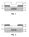
- FIGS. 1 and 2 Cross-sectional views of typical organic thin film transistor are shown in FIGS. 1 and 2 , wherein FIG. 1 illustrates a typical bottom contact configuration and FIG. 2 illustrates a typical top contact configuration.
- Each thin film transistor (TFT) in the embodiments of FIGS. 1 and 2 contains a source electrode 20, a drain electrode 30, a gate electrode 44, a gate dielectric 56, a substrate 28, and the semiconductor 70 used in the invention in the form of a film connecting the source electrode 20 to drain electrode 30, which semiconductor comprises a compound selected from the class of N,N'-di(arylalkyl) substituted 1,4,5,8- naphthalene tetracarboxylic acid diimide compounds described herein.
- the charges injected from the source electrode into the semiconductor are mobile and a current flows from source to drain, mainly in a thin channel region within 100 Angstroms of the semiconductor-dielectric interface. See A. Dodabalapur, L. Torsi H. E. Katz, Science 1995, 268, 270 , hereby incorporated by reference.
- the charge need only be injected laterally from the source electrode 20 to form the channel.
- the channel In the absence of a gate field the channel ideally has few charge carriers; as a result there is ideally no source-drain conduction.
- the off current is defined as the current flowing between the source electrode 20 and the drain electrode 30 when charge has not been intentionally injected into the channel by the application of a gate voltage. For an accumulation-mode TFT, this occurs for a gate-source voltage more negative, assuming an n-channel, than a certain voltage known as the threshold voltage. See Sze in Semiconductor Devices-Physics and Technology, John Wiley & Sons (1981), pages 438-443 .
- the on current is defined as the current flowing between the source electrode 20 and the drain electrode 30 when charge carriers have been accumulated intentionally in the channel by application of an appropriate voltage to the gate electrode 44, and the channel is conducting. For an n-channel accumulation-mode TFT, this occurs at gate-source voltage more positive than the threshold voltage.
- this threshold voltage is desirable for this threshold voltage to be zero, or slightly positive, for n-channel operation. Switching between on and off is accomplished by the application and removal of an electric field from the gate electrode 44 across the gate dielectric 56 to the semiconductor-dielectric interface, effectively charging a capacitor.
- the organic semiconductor materials used in the present invention when used in the form of an n-channel film, can exhibit high performance under inert conditions without the need for special chemical underlayers.
- the improved n- channel semiconductor film of the present invention comprising the N,N'-di(arylalkyl) 1,4,5,8-naphthalene-based tetracarboxylic acid diimide compounds, preferably N,N'-di(phenylalkyl)-1,4,5,8-naphthalene-based tetracarboxylic acid diimide compounds, described herein, is capable of exhibiting a field effect electron mobility greater than 0.5 cm 2 /Vs, preferably greater than 1.0 cm 2 /Vs. Most advantageously, such mobilities are exhibited in air.
- N,N'-di(arylalkyl) 1,4,5,8-naphthalene-based tetracarboxylic acid diimide compounds described have exhibited mobilities in the range of 0.5-5.0 cm 2 /Vs, for example 2.5 cm 2 /Vs, which are some of the highest thus far reported for n-channel semiconductor materials.
- films comprising the compounds of the present invention exhibit a field effect electron mobility that is greater than 0.01 cm 2 /Vs, preferably greater than 0.1 cm 2 /Vs, more preferably greater than 0.2 cm 2 /Vs.
- the n-channel semiconductor film used in the invention is capable of providing on/off ratios of at least 10 4 , advantageously at least 10 5 .
- the on/off ratio is measured as the maximum/minimum of the drain current as the gate voltage is swept from zero to 80 volts and the drain-source voltage is held at a constant value of 80 volts, and employing a silicon dioxide gate dielectric.
- these properties are attainable after repeated exposure of the n-type semiconductor material to air, before film deposition, as well as exposure of the transistor device and/or the channel layer to air after deposition.
- the solid-state structure of the material has the individual molecules packed such that the orbitals of the conjugated naphthalene core system containing the naphthalene ring system and/or the imide carboxyl groups, are able to interact with adjacent molecules, resulting in high mobility.
- the direction of this interaction has a component parallel to the direction of desired current flow in a device using this material as the active layer.
- the morphology of the films formed by the material is substantially continuous, such that current flows through the material without unacceptable interruption.
- the lowest lying unoccupied molecular orbital of the compound is at an energy that allows for injection of electrons at useful voltages from metals with reasonable work functions.
- This conjugated structure generally has a desirable lowest unoccupied molecular orbital (LUMO) energy level of 3.5 eV to 4.6 eV with reference to the vacuum energy level.
- LUMO energy level and reduction potential approximately describe the same characteristics of a material. LUMO energy level values are measured with reference to the vacuum energy level, and reduction potential values are measured in solution versus a standard electrode.
- An advantage for device applications is that the LUMO in the crystalline solid, which is the conduction band of the semiconductor, and the electron affinity of the solid both are measured with reference to the vacuum level. The latter parameters are usually different from the former parameters, which are obtained from solution.
- the present invention is directed to a thin film transistor comprising, a thin film of organic semiconductor material that comprises an N,N'-di(arylalkyl)-substituted naphthalene-based tetracarboxylic diimide compound of formula (I), wherein any optional substituents on the aryl rings comprises at least one electron donating organic group, i.e., if one or more substituents are present on one or both of the two carbocyclic ring systems, such substituents comprise at least one electron donating group.
- the two carbocyclic ring systems can differ, and each carbocyclic ring system can independently have different substitution or no substitution.
- each carbocyclic ring system is the same, although the substitution on each ring system, if any, may differ.
- both carbocyclic ring systems are substituted, then both carbocyclic ring systems comprise at least one electron donating substituent group.
- R 1 , R 2 , R 3 , R 4 , R 5 , R 6 , R 7 , R 8 , R 9 , and R 10 substituents on the phenyl rings comprise at least one electron donating substituent, more preferably an alkyl, most preferably a methyl group.
- Preferred organic groups include, for example, CH 3 , linear or branched C 2 -C 4 alkyl, alkylene (a monovalent unsaturated aliphatic hydrocarbon), and alkoxy.
- none of the R 1 to R 10 groups is an electronegative group such as a fluorine, trifluoromethyl or other fluorine-containing groups, nor an aryl substituent.
- X is a divalent hydrocarbon group having 1 to 4 carbon atoms, more preferably 1 to 3 carbon atoms.
- At least one phenyl ring is substituted with a single substituent (most preferably an alkyl group) that is ortho or meta to the position of the -(X) n - group in Structure I linking the phenyl and imide nitrogen. More preferably, both phenyl rings are substituted with a single substituent (most preferably an alkyl group) that is ortho or meta to the position of the -(X) n - group linking the phenyl and imide nitrogen.
- R 1 , R 2 , R 3 , R 4 and R 5 are H and at least two of R 6 , R 7 , R 8 , R 9 , and R 10 are H. More preferred structures are those in which at least three of R 1 , R 2 , R 3 , R 4 and R 5 are H and at least three of R 6 , R 7 , R 8 , R 9 , and R 10 are H.
- at least one phenyl group is substituted with an electron donating group.
- preferred structures are those in which either all of R 1 , R 3 , R 4 , R 5 , R 6 , R 8 , R 9 , and R 10 are H, and at least one of, preferably both of, R 2 and R 7 is an electron-donating group, preferably an alkyl group such as CH 3 ; or all of R 2 , R 3 , R 4 , R 5 , R 7 , R 8 , R 9 , and R 10 are H, and at least one of, preferably both of, R 1 and R 6 is an electron-donating group, preferably an alkyl group such as CH 3 .
- a first and second dicarboxylic imide moiety is attached on opposite sides of the naphthalene nucleus, at the 1,4 and 5,8 positions of the perylene nucleus, based on conventional numbering of the naphthalene nucleus.
- the naphthalene nucleus can be optionally substituted with up to four independently selected Y groups, wherein m is any integer from 0 to 4.
- the substituent groups Y can be an organic or inorganic group at any available position on the naphthalene nucleus. Preferably m is zero.
- the Y substituent groups on the naphthalene nucleus can include, for example, the following groups, which may be substituted or unsubstituted: alkyl groups, alkenyl, alkoxy groups, halogens such as fluorine or chlorine, cyano, aryl groups, arylalkyl groups, or any other groups that do not have a significantly adverse effect the n-type semiconductor properties of the film made from such compounds. It is advantageous to avoid substituents that tend to interfere with close approach of the conjugated cores of the compounds in a stacked arrangement of the molecules that is conducive to semiconductor properties.
- substituents include highly branched groups, ring structures and groups having more than 12 atoms, particularly where such groups or rings would be oriented to pose a significant steric barrier to the close approach of the conjugated cores.
- substituent groups should be avoided that substantially lower the solubility and/or volatility of the compounds such that the desirable fabrication processes are prevented.
- substituted or “substituent” means any group or atom other than hydrogen.
- group when used, it means that when a substituent group contains a substitutable hydrogen, it is also intended to encompass not only the substituents unsubstituted form, but also its form to the extent it can be further substituted (up to the maximum possible number) with any other mentioned substituent group or groups (mentioned for the same position) so long as the substituent does not destroy properties necessary for semiconductor utility. If desired, the substituents may themselves be further substituted one or more times with acceptable substituent groups.
- an alkyl group can be substituted with an alkoxy group, in the case of an R group (R 1 to R 10 ), or one or more fluorine atoms in the case of a Y group.
- R group R 1 to R 10
- Y group one or more fluorine atoms
- substituents may be joined together to form an aliphatic or unsaturated ring unless otherwise provided.
- examples of any of the above-mentioned alkyl groups are methyl, ethyl, propyl, isopropyl, butyl, isobutyl, t-butyl, pentyl, hexyl, octyl, 2- ethylhexyl, and congeners.
- Alkyl groups preferably having 1 to 6 carbon atoms, more preferably 1 to 4, are intended to include branched or linear groups.
- Alkenyl groups can be vinyl, 1-propenyl, 1-butenyl, 2-butenyl, and congeners.
- aryl groups can be phenyl, naphthyl, styryl, and congeners.
- Arylalkyl groups can be benzyl, phenethyl, and congeners.
- Useful substituents on any of the foregoing include halogen, and alkoxy, and the like.
- Y substituents on the naphthalene nucleus or core can be either electron-withdrawing groups and/or electron-donating groups.
- an electron donating group has a ⁇ p or ⁇ m of less than zero, more preferably less than -0.05, most preferably less than -0.1.
- the ⁇ p value can be used to indicate the electron donating nature of the group in a structure according to the present invention, as in Structure I above even when the group is not a para substituent in Structure I.
- Symmetrical N,N'-dialkyl naphthalene tetracarboxylic acid diimides used in this invention are conveniently prepared by cyclizing naphthalene tetracarboxylic acid dianhydride with excess of suitable amines such as phenylethyl amine.
- suitable amines such as phenylethyl amine.
- Typical procedures are described in Eur. Pat. Appl. EP 251071 and U. S. Pat. No. 4,156,757 and in U.S. Pat. Nos. 4,578,334 and 4,719,163 .
- Typical procedures for preparing unsymmetrical naphthalene tetracarboxylic acid diimides are described in U.S. Pat. No. 4,714,666 .
- the crude materials were then purified by train sublimation at 10 -5 to 10 -6 torr.
- a substrate is provided and a layer of the semiconductor material as described above can be applied to the substrate, electrical contacts being made with the layer.
- the exact process sequence is determined by the structure of the desired semiconductor component.
- a gate electrode can be first deposited on a flexible substrate, for example an organic polymer film, the gate electrode can then be insulated with a dielectric and then source and drain electrodes and a layer of the n-channel semiconductor material can be applied on top.
- the structure of such a transistor and hence the sequence of its production can be varied in the customary manner known to a person skilled in the art.
- a gate electrode can be deposited first, followed by a gate dielectric, then the organic semiconductor can be applied, and finally the contacts for the source electrode and drain electrode deposited on the semiconductor layer.
- a third structure could have the source and drain electrodes deposited first, then the organic semiconductor, with dielectric and gate electrode deposited on top.
- a field effect transistor comprises an insulating layer, a gate electrode, a semiconductor layer comprising an organic material as described herein, a source electrode, and a drain electrode, wherein the insulating layer, the gate electrode, the semiconductor layer, the source electrode, and the drain electrode are in any sequence as long as the gate electrode and the semiconductor layer both contact the insulating layer, and the source electrode and the drain electrode both contact the semiconductor layer.
- a support can be used for supporting the OTFT during manufacturing, testing, and/or use.
- a support selected for commercial embodiments may be different from one selected for testing or screening various embodiments.
- the support does not provide any necessary electrical function for the TFT.
- This type of support is termed a "non-participating support" in this document.
- Useful materials can include organic or inorganic materials.
- the support may comprise inorganic glasses, ceramic foils, polymeric materials, filled polymeric materials, coated metallic foils, acrylics, epoxies, polyamides, polycarbonates, polyimides, polyketones, poly(oxy-1,4- phenyleneoxy-1,4-phenylenecarbonyl-1,4-phenylene) (sometimes referred to as poly(ether ether ketone) or PEEK), polynorbornenes, polyphenyleneoxides, poly(ethylene naphthalenedicarboxylate) (PEN), poly(ethylene terephthalate) (PET), poly(phenylene sulfide) (PPS), and fiber-reinforced plastics (FRP).
- inorganic glasses ceramic foils, polymeric materials, filled polymeric materials, coated metallic foils, acrylics, epoxies, polyamides, polycarbonates, polyimides, polyketones, poly(oxy-1,4- phenyleneoxy-1,4-phenylenecarbonyl-1,4-phen
- a flexible support is used in some embodiments of the present invention. This allows for roll processing, which may be continuous, providing economy of scale and economy of manufacturing over flat and/or rigid supports.
- the flexible support chosen preferably is capable of wrapping around the circumference of a cylinder of less than 50 cm diameter, more preferably 25 cm diameter, most preferably 10 cm diameter, without distorting or breaking, using low force as by unaided hands.
- the preferred flexible support may be rolled upon itself.
- the support is optional.
- the support in a top construction as in FIG. 2 , when the gate electrode and/or gate dielectric provides sufficient support for the intended use of the resultant TFT, the support is not required.
- the support may be combined with a temporary support.
- a support may be detachably adhered or mechanically affixed to the support, such as when the support is desired for a temporary purpose, e.g., manufacturing, transport, testing, and/or storage.
- a flexible polymeric support may be adhered to a rigid glass support, which support could be removed.
- the gate electrode can be any useful conductive material.
- the gate electrode may comprise doped silicon, or a metal, such as aluminum, chromium, gold, silver, nickel, palladium, platinum, tantalum, and titanium.
- Conductive polymers also can be used, for example polyaniline, poly(3,4-ethylenedioxythiophene)/poly(styrene sulfonate) (PEDOT:PSS).
- PEDOT:PSS poly(3,4-ethylenedioxythiophene)/poly(styrene sulfonate)
- alloys, combinations, and multilayers of these materials may be useful.
- the same material can provide the gate electrode function and also provide the support function of the support.
- doped silicon can function as the gate electrode and support the OTFT.
- the gate dielectric is provided on the gate electrode. This gate dielectric electrically insulates the gate electrode from the balance of the OTFT device.
- the gate dielectric comprises an electrically insulating material.
- the gate dielectric should have a suitable dielectric constant that can vary widely depending on the particular device and circumstance of use. For example, a dielectric constant from 2 to 100 or even higher is known for a gate dielectric.
- Useful materials for the gate dielectric may comprise, for example, an inorganic electrically insulating material.
- the gate dielectric may comprise a polymeric material, such as polyvinylidenedifluoride (PVDF), cyanocelluloses, polyimides, etc.
- the gate electric may comprise a plurality of layers of different materials having different dielectric constants.
- materials useful for the gate dielectric include strontiates, tantalates, titanates, zirconates, aluminum oxides, silicon oxides, tantalum oxides, titanium oxides, silicon nitrides, barium titanate, barium strontium titanate, barium zirconate titanate, zinc selenide, and zinc sulfide.
- alloys, combinations, and multilayers of these examples can be used for the gate dielectric.
- aluminum oxides, silicon oxides, and zinc selenide are preferred.
- polymeric materials such as polyimides, and insulators that exhibit a high dielectric constant. Such insulators are discussed in U.S Pat. No. 5,981,970 hereby incorporated by reference.
- the gate dielectric can be provided in the OTFT as a separate layer, or formed on the gate such as by oxidizing the gate material to form the gate dielectric.
- the dielectric layer may comprise two or more layers having different dielectric constants.
- the source electrode and drain electrode are separated from the gate electrode by the gate dielectric, while the organic semiconductor layer can be over or under the source electrode and drain electrode.
- the source and drain electrodes can be any useful conductive material. Useful materials include most of those materials described above for the gate electrode, for example, aluminum, barium, calcium, chromium, gold, silver, nickel, palladium, platinum, titanium, polyaniline, PEDOT:PSS, other conducting polymers, alloys thereof, combinations thereof, and multilayers thereof.
- the thin film electrodes can be provided by any useful means such as physical vapor deposition (e.g., thermal evaporation, sputtering) or ink jet printing.
- the patterning of these electrodes can be accomplished by known methods such as shadow masking, additive photolithography, subtractive photolithography, printing, microcontact printing, and pattern coating.
- the organic semiconductor layer can be provided over or under the source and drain electrodes, as described above in reference to the thin film transistor article.
- the present invention also provides an integrated circuit comprising a plurality of OTFTs made by the process described herein.
- the n-channel semiconductor material made using the above-described N,N'-substituted 1,4,5,8-naphthalene-based tetracarboxylic acid diimide compounds are capable of being formed on any suitable substrate which can comprise the support and any intermediate layers such as a dielectric or insulator material, including those known in the art.
- the entire process of making the thin film transistor or integrated circuit of the present invention can be carried out below a maximum support temperature of 450° C, preferably below 250° C, more preferably below 150° C, and even more preferably below 100° C, or even at temperatures around room temperature (25° C to 70°C).
- the temperature selection generally depends on the support and processing parameters known in the art, once one is armed with the knowledge of the present invention contained herein. These temperatures are well below traditional integrated circuit and semiconductor processing temperatures, which enables the use of any of a variety of relatively inexpensive supports, such as flexible polymeric supports.
- the invention enables production of relatively inexpensive integrated circuits containing organic thin film transistors with significantly improved performance.
- Compounds used in the invention can be readily processed and are thermally stable to such as extent that they can be vaporized.
- the compounds possess significant volatility, so that vapor phase deposition, where desired, is readily achieved.
- Such compounds can be deposited onto substrates by vacuum sublimation.
- Deposition by a rapid sublimation method is also possible.
- One such method is to apply a vacuum of 35 mtorr to a chamber containing a substrate and a source vessel that holds the compound in powdered form, and heat the vessel over several minutes until the compound sublimes onto the substrate.
- the most useful compounds form well-ordered films, with amorphous films being less useful.
- TFTs thin film transistors
- organic field effect thin-film transistors devices in which the n-channel semiconductor films used in the invention are useful
- TFTs thin film transistors
- organic field effect thin-film transistors devices in which the n-channel semiconductor films used in the invention are useful
- TFTs thin film transistors
- organic field effect thin-film transistors devices in which the n-channel semiconductor films used in the invention are useful
- TFTs thin film transistors
- organic field effect thin-film transistors can be used in various types of devices having organic p-n junctions, such as described on pages 13 to 15 of US 2004,0021204 A1 to Liu , which patent is hereby incorporated by reference.
- TFTs and other devices include, for example, more complex circuits, e.g., shift registers, integrated circuits, logic circuits, smart cards, memory devices, radio-frequency identification tags, backplanes for active matrix displays, active-matrix displays (e.g. liquid crystal or OLED), solar cells, ring oscillators, and complementary circuits, such as inverter circuits, for example, in combination with other transistors made using available p-type organic semiconductor materials such as pentacene.
- a transistor according to the present invention can be used as part of voltage hold circuitry of a pixel of the display.
- TFTs are operatively connected by means known in the art.
- the present invention further provides a method of making any of the electronic devices described above.
- the present invention is embodied in an article that comprises one or more of the TFTs described.
- N,N'-di(arylalkyl)- 1,4,5,8-naphthalene tetracarboxylic acid diimides used in this invention are conveniently prepared by cyclizing naphthalene tetracarboxylic acid dianhydride with excess 2-para-tolyl-ethylamine following a general method described in Rademacher, A. et al. Chem. Ber. 1982 115, 2927 .
- N,N'-di(4-methylphenyl)ethyl- 1,4,5,8-naphthalene tetracarboxylic acid diimide used in this invention is conveniently prepared by cyclizing naphthalene tetracarboxylic acid dianhydride with excess 2-para-tolyl-ethylamine.
- naphthalene tetracarboxylic acid dianhydride which is available from Aldrich Chemical Company, 3-4 equivalents excess of an amine, for example 2-para-tolyl-ethylamine, also available from Aldrich, zinc acetate in catalytic amounts, and 10-15 ml of quinoline per gram of dianhydride molecule was heated over 4-5 hours at a temperature of ca. 220°C.
- the mixture is allowed to cool to room temperature, and the precipitated solids are collected, filtered and washed with acetone, followed by 200 ml each of boiling 0.1 M aqueous Na 2 CO 3 , boiling water, and warm toluene, that is kept below the temperature at which the product would be substantially dissolved.
- the solid is then purified by train sublimation at 10 -5 to 10 -6 torr. (As described above, other compounds are conveniently prepared by cyclizing naphthalene tetracarboxylic acid dianhydride with excess of the suitable amine.)
- the crude materials were then purified by train sublimation at 10 -5 to 10 -6 torr.
- field-effect transistors were typically made using the top-contact geometry.
- the substrate used is a heavily doped silicon wafer, which also serves as the gate of the transistor.
- the gate dielectric is a thermally grown SiO 2 layer with a thickness of 185 nm. It has been previously shown for both p-type and n-type transistors that electrical properties can be improved by treating the surface of the gate dielectric. For most of the experiments described here, the oxide surface was treated with a thin ( ⁇ 10 nm), spin-coated polymer layer, or a self-assembled monolayer (SAM) of octadecyltrichlorosilane (OTS). Typically, an untreated oxide sample was included in the experiments for comparison.
- SAM self-assembled monolayer
- OTS octadecyltrichlorosilane
- the active layer of naphthalene tetracarboxylic acid diimide was deposited via vacuum deposition in a thermal evaporator. The deposition rate was 0.1 Angstroms per second while the substrate temperature was held at 90°C for most experiments. The thickness of the active layer was a variable in some experiments, but was typically 25 nm. Silver contacts of thickness 50 nm were deposited through a shadow mask. The channel width was held at 420 microns, while the channel lengths were varied between 50 and 175 microns. Some experiments were performed to look at the effect of other contact materials. A few devices were made with a bottom-contact geometry, in which the contacts were deposited prior to the active material.
- the drain current (Id) was measured as a function of source-drain voltage (Vd) for various values of gate voltage (Vg).
- Vd was swept from 0 V to 80 V for each of the gate voltages measured, typically 0 V, 20 V, 40 V, 60 V, and 80 V.
- the gate current (Ig) was also recorded in order to detect any leakage current through the device.
- the drain current was measured as a function of gate voltage for various values of source-drain voltage.
- Vg was swept from 0 V to 80 V for each of the drain voltages measured, typically 40 V, 60 V, and 80 V.
- Parameters extracted from the data include field-effect mobility ( ⁇ ), threshold voltage (Vth), subthreshold slope (S), and the ratio of Ion/Ioff for the measured drain current.
- the field-effect mobility was extracted in the saturation region, where Vd > Vg - Vth.
- W and L are the channel width and length, respectively
- C ox is the capacitance of the oxide layer, which is a function of oxide thickness and dielectric constant of the material.
- the saturation field-effect mobility was extracted from a straight-line fit to the linear portion of the ⁇ I d versus Vg curve.
- the threshold voltage, V th is the x-intercept of this straight-line fit. Mobilities can also be extracted from the linear region, where Vd ⁇ Vg- Vth.
- the log of the drain current as a function of gate voltage was plotted. Parameters extracted from the log I d plot include the I on /I off ratio and the sub-threshold slope (S).
- the I on /I off ratio is simply the ratio of the maximum to minimum drain current, and S is the inverse of the slope of the I d curve in the region over which the drain current is increasing (i.e. the device is turning on).
- inventive devices comprising arylalkyl-containing N,N'-substituted-1,4,5,8-naphthalene-based tetracarboxylic acid diimides provide improved n- channel semiconductor films having high mobility and on/off ratio.
- the mobility calculated in the saturation region was between 0.07 and 2.5 cm 2 /Vs, with an on/off ratio of 10 4 to 10 5 .
- the devices also show improved stability in air relative to typical n-channel TFTs, and excellent reproducibility.
- This example demonstrates the n-type TFT device made from an N,N'-diphenyl-1,4,5,8-naphthalene tetracarboxylic acid diimide C-1:
- a heavily doped silicon wafer with a thermally-grown SiO 2 layer with a thickness of 185 nm was used as the substrate.
- the wafer was cleaned for 10 minutes in a piranah solution, followed by a 6-minute exposure in a UV/ozone chamber.
- the cleaned surface was then treated with a self-assembled monolayer of octadecyltrichlorosilane (OTS), made from a heptane solution under a humidity-controlled environment. Water contact angles and layer thicknesses were measured to ensure the quality of the treated surface. Surfaces with a good quality OTS layer have water contact angles > 90°, and thicknesses determined from ellipsometry in the range of 27 ⁇ to 35 ⁇ .
- the purified N,N'-diphenyl-1,4,5,8-naphthalene tetracarboxylic acid diimide C-1 was deposited by vacuum sublimation at a pressure of 2 x 10 -7 Torr and a rate of 0.1 Angstroms per second to a thickness of 25 nm as measured by a quartz crystal. During deposition the substrate was held at a constant temperature of 90°C. The sample was exposed to air for a short time prior to subsequent deposition of Ag source and drain electrodes through a shadow mask to a thickness of 50 nm. The devices made had a 420 micron channel width, with channel lengths varying from 50 to 175 microns. Multiple OTFTs were prepared and representative samples of 4 to 12 OTFTs were tested for each deposition run. The averaged results appear in Table 1 below.
- the devices were exposed to air prior to measurement in an argon atmosphere using a Hewlett-Packard 4145B® semiconductor parameter analyzer.
- the field effect mobility, ⁇ was calculated from the slope of the (I D ) 1 ⁇ 2 versus V G plot.
- the average mobility was found to be 0.064 cm 2 /Vs in the saturation region.
- the average on-off ratio was 2.3 x 10 4, and the average threshold voltage was 57.3V. Saturation mobilities of up to 0.12 cm 2 /Vs were measured for devices prepared in this way.
- This example demonstrates the improved performance of an n-type TFT device using N,N'-di(phenylethyl)-1,4,5,8-naphthalene tetracarboxylic acid diimide, Compound I-1 in accordance with the present invention.
- n-type TFT device comprising Compound I-1 as the active material was made as in Example 1. Accordingly, compound I-1 was deposited by vacuum sublimation at a pressure of 2 ⁇ 10 -7 Torr and a rate of 0.1 Angstroms per second to a thickness of 25 nm as measured by a quartz crystal. During deposition the substrate was held at a constant temperature of 90 °C. The sample was exposed to air for a short time prior to subsequent deposition of Ag source and drain electrodes through a shadow mask to a thickness of 50 nm. The devices made had an approximately 420 micron channel width, with channel lengths varying from 50 to 175 microns. Multiple organic thin film transistors (OTFTs) were prepared and representative sample of 4 to 12 OTFTs were tested for each deposition run. The averaged results appear in Table 1 below.
- the devices were exposed to air prior to measurement in an argon atmosphere using a Hewlett-Packard 4145B® semiconductor parameter analyzer.
- the average field effect mobility, ⁇ was calculated from the slope of the (I D ) 1 ⁇ 2 versus V G plot to be 0.13 cm 2 /Vs in the saturation region.
- This example demonstrates the improved performance n-type TFT device made from a fluorine-containing N,N'-di(4-methylphenyl)ethyl- 1,4,5,8-naphthalene tetracarboxylic acid diimide, Compound I-4.
- An n-type TFT device using compound I-4 as the active material of the OTFT was made as in Example 1. Multiple OTFTs were prepared and tested for each deposition run. The averaged results appear in Table 2 below.
- This example demonstrates the improved performance n-type TFT device made from N,N'-di(2-phenyl-propyl)-1,4,5,8-naphthalene tetracarboxylic acid diimide, Compound I-15.
- An n-type TFT device using Compound I-15 as the active material of the OTFT was made as in Example 1. Multiple OTFTs were prepared and tested for each deposition run. The averaged results appear in Table 3 below.
- This example demonstrates the improved performance n-type TFT device made from N,N'-di(3-methylphenyl)ethyl-1,4,5,8-naphthalene tetracarboxylic acid diimide, Compound I-2.
- An n-type TFT device using Compound I-2 as the active material of the OTFT was made as in Example 1. Multiple OTFTs were prepared and tested for each deposition run. The averaged results appear in Table 4 below.
Landscapes
- Engineering & Computer Science (AREA)
- Chemical & Material Sciences (AREA)
- Nanotechnology (AREA)
- Physics & Mathematics (AREA)
- Materials Engineering (AREA)
- Crystallography & Structural Chemistry (AREA)
- Spectroscopy & Molecular Physics (AREA)
- Composite Materials (AREA)
- Condensed Matter Physics & Semiconductors (AREA)
- General Physics & Mathematics (AREA)
- Mathematical Physics (AREA)
- Theoretical Computer Science (AREA)
- Organic Chemistry (AREA)
- Thin Film Transistor (AREA)
Abstract
Claims (9)
- Transistor en couches minces comprenant une mince couche de matériau semi-conducteur organique constitué d'un composé 1,4,5,8-naphtalène tétracarboxylique diimide substitué par un composé N,N'-di(arylalkyle) représenté par la structure suivante de formule (I) :

où Y est indépendamment choisi parmi les groupes alkyle, alcényle et alcoxy et m est un entier de 0 à 4 ; et
dans lequel éventuellement deux groupes adjacents sur ledit premier ou ledit second système cyclique peuvent se combiner pour former un cycle aromatique condensé. - Transistor en couches minces selon la revendication 1, dans lequel soit l'un soit les deux systèmes sélectionnés parmi les premier et second systèmes cycliques de ladite structure sont substitués par au moins un groupe donneur d'électrons.
- Transistor en couches minces selon la revendication 2, dans lequel le ou les groupe(s) donneur(s) d'électrons est (sont) un groupe alkyle.
- Transistor en couches minces selon la revendication 1, dans lequel, dans ladite structure, R1, R2, R3, R4, R5, R6, R7, R8, R9, et R10 sont chacun indépendamment sélectionnés parmi H, CH3, un groupe alkyle, alcényle, alcoxy en C2-C4 linéaire ou ramifié ou un autre groupe organique donneur d'électrons de 1 à 4 atomes de carbone.
- Transistor en couches minces selon la revendication 1, dans lequel, dans ladite structure, les premier et second systèmes cycliques sont un cycle phényle non condensé substitué ou non.
- Transistor en couches minces selon la revendication 5, dans lequel, dans ladite structure, au moins un cycle phényle est substitué par un substituant unique qui est en position ortho ou méta par rapport à la position du groupe -(X)n- reliant le groupe phényle et l'imide azote.
- Transistor en couches minces selon la revendication 5, dans lequel, dans ladite structure, les deux cycles phényle sont substitués par un substituant unique qui est en position ortho ou méta par rapport à la position du groupe -(X)n- reliant le groupe phényle et l'imide azote.
- Transistor en couches minces selon l'une quelconque des revendications précédentes, dans lequel le transistor en couches minces est un transistor à effet de champ comprenant une couche diélectrique, une électrode de grille, une électrode de source et une électrode de drain et dans lequel la couche diélectrique, l'électrode de grille, la couche mince de matériau semi-conducteur organique, l'électrode de source et l'électrode de drain sont placées dans n'importe quel ordre tant que l'électrode de grille et la couche de matériau semi-conducteur organique sont toutes deux en contact avec la couche diélectrique, et l'électrode de source et l'électrode de drain sont toutes deux en contact avec la couche mince de matériau semi-conducteur organique.
- Procédé de fabrication d'un dispositif semi-conducteur en couches minces comprenant les étapes suivantes, pas nécessairement dans l'ordre suivant :(a) déposer sur un substrat, une couche mince de matériau semi-conducteur organique à canal n constitué d'un composé diimide naphtalène tétracarboxylique substitué par un composé N,N'-di(arylalkyle) selon la revendication 1, dans lequel les substituants, s'il y en a, sur chaque système cyclique sont des groupes organiques donneurs d'électrons, de sorte que le matériau semi-conducteur organique présente une mobilité des électrons à effet de champ supérieure à 0,01 cm2/Vs ;(b) former une électrode de source et une électrode de drain séparées l'une de l'autre, dans lequel l'électrode de source et l'électrode de grain sont séparées par le, et reliées par voie électrique, au film semi-conducteur à canal n ; et(c) former une électrode de grille séparée du matériau semi-conducteur organique.
Applications Claiming Priority (2)
| Application Number | Priority Date | Filing Date | Title |
|---|---|---|---|
| US11/110,076 US7579619B2 (en) | 2005-04-20 | 2005-04-20 | N,N′-di(arylalkyl)-substituted naphthalene-based tetracarboxylic diimide compounds as n-type semiconductor materials for thin film transistors |
| PCT/US2006/012520 WO2006115714A1 (fr) | 2005-04-20 | 2006-04-05 | Matériaux semi-conducteurs pour des transistors à couche fine |
Publications (2)
| Publication Number | Publication Date |
|---|---|
| EP1872416A1 EP1872416A1 (fr) | 2008-01-02 |
| EP1872416B1 true EP1872416B1 (fr) | 2010-05-05 |
Family
ID=36754252
Family Applications (1)
| Application Number | Title | Priority Date | Filing Date |
|---|---|---|---|
| EP06740494A Not-in-force EP1872416B1 (fr) | 2005-04-20 | 2006-04-05 | Matériaux semi-conducteurs pour des transistors à couche mince |
Country Status (7)
| Country | Link |
|---|---|
| US (2) | US7579619B2 (fr) |
| EP (1) | EP1872416B1 (fr) |
| JP (1) | JP2008538653A (fr) |
| KR (1) | KR20080003813A (fr) |
| DE (1) | DE602006014128D1 (fr) |
| TW (1) | TW200644304A (fr) |
| WO (1) | WO2006115714A1 (fr) |
Families Citing this family (29)
| Publication number | Priority date | Publication date | Assignee | Title |
|---|---|---|---|---|
| EP1749316B1 (fr) * | 2004-01-26 | 2016-06-29 | Northwestern University | Semi-conducteurs de type perylene n et dispositifs associes |
| BRPI0615930A2 (pt) * | 2005-09-15 | 2016-08-23 | Painceptor Pharma Corp | métodos de modular a interação de uma neurotrofina e um receptor de neurotrofina, de tratar dor em um indivíduo, de tratar distúrbio inflamatório em um indivíduo, de tratar um distúrbio neurológico em um indivíduo, e de tratar uma doença ou distúrbio associado aos sistemas geniturinário e/ou gastrointestinal de um indivíduo, e, composto |
| US7422777B2 (en) * | 2005-11-22 | 2008-09-09 | Eastman Kodak Company | N,N′-dicycloalkyl-substituted naphthalene-based tetracarboxylic diimide compounds as n-type semiconductor materials for thin film transistors |
| US8138075B1 (en) | 2006-02-06 | 2012-03-20 | Eberlein Dietmar C | Systems and methods for the manufacture of flat panel devices |
| US7569693B2 (en) * | 2006-06-12 | 2009-08-04 | Northwestern University | Naphthalene-based semiconductor materials and methods of preparing and use thereof |
| JP5091449B2 (ja) * | 2006-10-03 | 2012-12-05 | 株式会社日立製作所 | 単分子を利用した有機トランジスタ及びfet |
| EP2089398A2 (fr) * | 2006-10-25 | 2009-08-19 | Polyera Corporation | Matériaux semiconducteurs organiques et leurs procédés de préparation et d'utilisation |
| WO2008063583A1 (fr) * | 2006-11-17 | 2008-05-29 | Polyera Corporation | Matériaux semi-conducteurs organiques à base d'acène et procédés de préparation et d'utilisation de ceux-ci |
| JP5380296B2 (ja) | 2006-11-17 | 2014-01-08 | ポリエラ コーポレイション | ジイミド系半導体材料ならびにジイミド系半導体材料を調製および使用する方法 |
| JP2010515684A (ja) * | 2007-01-08 | 2010-05-13 | ポリエラ コーポレイション | アレーン−ビス(ジカルボキシイミド)系半導体材料、およびそれを調製するための関連する中間体を調製する方法 |
| US8022214B2 (en) * | 2007-01-24 | 2011-09-20 | Polyera Corporation | Organic semiconductor materials and precursors thereof |
| JP5117763B2 (ja) * | 2007-05-21 | 2013-01-16 | 山本化成株式会社 | 有機トランジスタ |
| WO2009089283A2 (fr) * | 2008-01-07 | 2009-07-16 | The Johns Hopkins University | Transistors hybrides à canal n à faible tension |
| US7649199B2 (en) * | 2008-04-11 | 2010-01-19 | Eastman Kodak Company | N-type semiconductor materials in thin film transistors and electronic devices |
| EP2448033A4 (fr) * | 2009-06-23 | 2014-07-23 | Sumitomo Chemical Co | Elément électroluminescent organique |
| EP2492271B1 (fr) * | 2009-10-23 | 2018-05-09 | Shanghai Institute Of Organic Chemistry, Chinese Academy Of Sciences | Dérivés de diimide d'acide naphtalène-tétracarboxylique condensé avec un hétérocycle contenant du soufre, procédé de préparation et utilisation de ceux-ci |
| US8212243B2 (en) | 2010-01-22 | 2012-07-03 | Eastman Kodak Company | Organic semiconducting compositions and N-type semiconductor devices |
| US8530270B2 (en) | 2010-04-30 | 2013-09-10 | Eastman Kodak Company | Methods of preparing semiconductive compositions and devices |
| US8411489B2 (en) | 2010-04-30 | 2013-04-02 | Eastman Kodak Company | Semiconducting devices and methods of preparing |
| US20110269966A1 (en) | 2010-04-30 | 2011-11-03 | Deepak Shukla | Semiconducting articles |
| US8314265B2 (en) | 2010-04-30 | 2012-11-20 | Eastman Kodak Company | Aromatic amic acids or amic esters and compositions |
| US8404892B2 (en) | 2010-05-27 | 2013-03-26 | Eastman Kodak Company | Aromatic amic acid salts and compositions |
| US8431433B2 (en) | 2010-05-27 | 2013-04-30 | Eastman Kodak Company | Methods of providing semiconductor layers from amic acid salts |
| US8450726B2 (en) | 2010-05-27 | 2013-05-28 | Eastman Kodak Company | Articles containing coatings of amic acid salts |
| US8692238B2 (en) | 2012-04-25 | 2014-04-08 | Eastman Kodak Company | Semiconductor devices and methods of preparation |
| US8779415B2 (en) | 2012-11-08 | 2014-07-15 | Eastman Kodak Company | Devices containing organic polymeric multi-metallic composites |
| CN103623741B (zh) * | 2013-11-27 | 2015-05-20 | 中国科学院长春应用化学研究所 | 石墨烯分散剂、其制备方法及石墨烯的制备方法 |
| US20150352828A1 (en) | 2014-06-09 | 2015-12-10 | Gregory L. Zwadlo | Reducing print line width on flexo plates |
| WO2015191293A1 (fr) | 2014-06-11 | 2015-12-17 | Eastman Kodak Company | Dispostifs dotés de couches diélectriques polymériques de thiosulfate |
Family Cites Families (10)
| Publication number | Priority date | Publication date | Assignee | Title |
|---|---|---|---|---|
| DE2951349A1 (de) | 1979-12-20 | 1981-07-02 | Bayer Ag, 5090 Leverkusen | Naphthalintetracarbonsaeurediimide als elektrische halbleiter und photoleiter |
| US4611385A (en) * | 1982-06-18 | 1986-09-16 | At&T Bell Laboratories | Devices formed utilizing organic materials |
| US4468444A (en) * | 1983-04-21 | 1984-08-28 | Eastman Kodak Company | Pyrylium-sensitized leuco base photoconductive compositions and elements containing naphthalene bis-dicarboximide compounds |
| FR2664430B1 (fr) | 1990-07-04 | 1992-09-18 | Centre Nat Rech Scient | Transistor a effet de champ en couche mince de structure mis, dont l'isolant et le semiconducteur sont realises en materiaux organiques. |
| JP3373783B2 (ja) * | 1998-05-29 | 2003-02-04 | 京セラミタ株式会社 | ナフタレンテトラカルボン酸ジイミド誘導体及び電子写真用感光体 |
| US6387727B1 (en) * | 1999-03-29 | 2002-05-14 | Agere Systems Guardian Corp. | Device comprising n-channel semiconductor material |
| US7026643B2 (en) * | 2001-05-04 | 2006-04-11 | International Business Machines Corporation | Organic n-channel semiconductor device of N,N' 3,4,9,10 perylene tetracarboxylic diimide |
| US6946677B2 (en) * | 2002-06-14 | 2005-09-20 | Nokia Corporation | Pre-patterned substrate for organic thin film transistor structures and circuits and related method for making same |
| JP4405970B2 (ja) * | 2003-12-26 | 2010-01-27 | キヤノン株式会社 | 電子写真感光体、プロセスカートリッジおよび電子写真装置 |
| EP1749316B1 (fr) * | 2004-01-26 | 2016-06-29 | Northwestern University | Semi-conducteurs de type perylene n et dispositifs associes |
-
2005
- 2005-04-20 US US11/110,076 patent/US7579619B2/en active Active
-
2006
- 2006-04-05 JP JP2008507692A patent/JP2008538653A/ja active Pending
- 2006-04-05 WO PCT/US2006/012520 patent/WO2006115714A1/fr active Application Filing
- 2006-04-05 EP EP06740494A patent/EP1872416B1/fr not_active Not-in-force
- 2006-04-05 DE DE602006014128T patent/DE602006014128D1/de active Active
- 2006-04-05 KR KR1020077023838A patent/KR20080003813A/ko not_active Application Discontinuation
- 2006-04-19 TW TW095113884A patent/TW200644304A/zh unknown
-
2009
- 2009-05-29 US US12/474,533 patent/US7981719B2/en not_active Expired - Fee Related
Also Published As
| Publication number | Publication date |
|---|---|
| WO2006115714A1 (fr) | 2006-11-02 |
| JP2008538653A (ja) | 2008-10-30 |
| TW200644304A (en) | 2006-12-16 |
| US20090261323A1 (en) | 2009-10-22 |
| EP1872416A1 (fr) | 2008-01-02 |
| DE602006014128D1 (de) | 2010-06-17 |
| US7981719B2 (en) | 2011-07-19 |
| US7579619B2 (en) | 2009-08-25 |
| KR20080003813A (ko) | 2008-01-08 |
| US20060237712A1 (en) | 2006-10-26 |
Similar Documents
| Publication | Publication Date | Title |
|---|---|---|
| EP1872416B1 (fr) | Matériaux semi-conducteurs pour des transistors à couche mince | |
| EP1952453B1 (fr) | Diimides tetracarboxyliques a base de naphtalene comme materiaux semi-conducteurs | |
| US7629605B2 (en) | N-type semiconductor materials for thin film transistors | |
| EP2089919B1 (fr) | Composés diimide tétracarboxyliques contenant du naphtalène utilisés comme matériaux semi-conducteurs | |
| US7326956B2 (en) | Fluorine-containing N,N′-diaryl perylene-based tetracarboxylic diimide compounds as N-type semiconductor materials for thin film transistors | |
| US7745821B2 (en) | Aryl dicarboxylic acid diimidazole-based compounds as n-type semiconductor materials for thin film transistors | |
| US7198977B2 (en) | N,N′-di(phenylalky)-substituted perylene-based tetracarboxylic diimide compounds as n-type semiconductor materials for thin film transistors | |
| US7858970B2 (en) | Heterocycloalkyl-substituted naphthalene-based tetracarboxylic diimide compounds as N-type semiconductor materials for thin film transistors |
Legal Events
| Date | Code | Title | Description |
|---|---|---|---|
| PUAI | Public reference made under article 153(3) epc to a published international application that has entered the european phase |
Free format text: ORIGINAL CODE: 0009012 |
|
| 17P | Request for examination filed |
Effective date: 20070924 |
|
| AK | Designated contracting states |
Kind code of ref document: A1 Designated state(s): DE FR GB |
|
| 17Q | First examination report despatched |
Effective date: 20080128 |
|
| DAX | Request for extension of the european patent (deleted) | ||
| RBV | Designated contracting states (corrected) |
Designated state(s): DE FR GB |
|
| GRAP | Despatch of communication of intention to grant a patent |
Free format text: ORIGINAL CODE: EPIDOSNIGR1 |
|
| GRAS | Grant fee paid |
Free format text: ORIGINAL CODE: EPIDOSNIGR3 |
|
| GRAA | (expected) grant |
Free format text: ORIGINAL CODE: 0009210 |
|
| AK | Designated contracting states |
Kind code of ref document: B1 Designated state(s): DE FR GB |
|
| REG | Reference to a national code |
Ref country code: GB Ref legal event code: FG4D |
|
| REF | Corresponds to: |
Ref document number: 602006014128 Country of ref document: DE Date of ref document: 20100617 Kind code of ref document: P |
|
| PLBE | No opposition filed within time limit |
Free format text: ORIGINAL CODE: 0009261 |
|
| STAA | Information on the status of an ep patent application or granted ep patent |
Free format text: STATUS: NO OPPOSITION FILED WITHIN TIME LIMIT |
|
| 26N | No opposition filed |
Effective date: 20110208 |
|
| REG | Reference to a national code |
Ref country code: DE Ref legal event code: R097 Ref document number: 602006014128 Country of ref document: DE Effective date: 20110207 |
|
| PGFP | Annual fee paid to national office [announced via postgrant information from national office to epo] |
Ref country code: GB Payment date: 20130326 Year of fee payment: 8 |
|
| PGFP | Annual fee paid to national office [announced via postgrant information from national office to epo] |
Ref country code: FR Payment date: 20130417 Year of fee payment: 8 |
|
| GBPC | Gb: european patent ceased through non-payment of renewal fee |
Effective date: 20140405 |
|
| REG | Reference to a national code |
Ref country code: FR Ref legal event code: ST Effective date: 20141231 |
|
| PG25 | Lapsed in a contracting state [announced via postgrant information from national office to epo] |
Ref country code: GB Free format text: LAPSE BECAUSE OF NON-PAYMENT OF DUE FEES Effective date: 20140405 |
|
| PG25 | Lapsed in a contracting state [announced via postgrant information from national office to epo] |
Ref country code: FR Free format text: LAPSE BECAUSE OF NON-PAYMENT OF DUE FEES Effective date: 20140430 |
|
| PGFP | Annual fee paid to national office [announced via postgrant information from national office to epo] |
Ref country code: DE Payment date: 20150429 Year of fee payment: 10 |
|
| REG | Reference to a national code |
Ref country code: DE Ref legal event code: R119 Ref document number: 602006014128 Country of ref document: DE |
|
| PG25 | Lapsed in a contracting state [announced via postgrant information from national office to epo] |
Ref country code: DE Free format text: LAPSE BECAUSE OF NON-PAYMENT OF DUE FEES Effective date: 20161101 |