EP1869769B1 - Verbesserter hochfrequenz-digital/analog-umsetzer - Google Patents
Verbesserter hochfrequenz-digital/analog-umsetzer Download PDFInfo
- Publication number
- EP1869769B1 EP1869769B1 EP04786460.8A EP04786460A EP1869769B1 EP 1869769 B1 EP1869769 B1 EP 1869769B1 EP 04786460 A EP04786460 A EP 04786460A EP 1869769 B1 EP1869769 B1 EP 1869769B1
- Authority
- EP
- European Patent Office
- Prior art keywords
- switch
- circuit
- current
- digital
- transistor
- Prior art date
- Legal status (The legal status is an assumption and is not a legal conclusion. Google has not performed a legal analysis and makes no representation as to the accuracy of the status listed.)
- Expired - Lifetime
Links
Images








Classifications
-
- H—ELECTRICITY
- H03—ELECTRONIC CIRCUITRY
- H03F—AMPLIFIERS
- H03F3/00—Amplifiers with only discharge tubes or only semiconductor devices as amplifying elements
- H03F3/34—DC amplifiers in which all stages are DC-coupled
- H03F3/343—DC amplifiers in which all stages are DC-coupled with semiconductor devices only
- H03F3/3432—DC amplifiers in which all stages are DC-coupled with semiconductor devices only with bipolar transistors
-
- H—ELECTRICITY
- H03—ELECTRONIC CIRCUITRY
- H03F—AMPLIFIERS
- H03F1/00—Details of amplifiers with only discharge tubes, only semiconductor devices or only unspecified devices as amplifying elements
- H03F1/08—Modifications of amplifiers to reduce detrimental influences of internal impedances of amplifying elements
- H03F1/22—Modifications of amplifiers to reduce detrimental influences of internal impedances of amplifying elements by use of cascode coupling, i.e. earthed cathode or emitter stage followed by earthed grid or base stage respectively
-
- H—ELECTRICITY
- H03—ELECTRONIC CIRCUITRY
- H03M—CODING; DECODING; CODE CONVERSION IN GENERAL
- H03M1/00—Analogue/digital conversion; Digital/analogue conversion
- H03M1/06—Continuously compensating for, or preventing, undesired influence of physical parameters
- H03M1/08—Continuously compensating for, or preventing, undesired influence of physical parameters of noise
- H03M1/0863—Continuously compensating for, or preventing, undesired influence of physical parameters of noise of switching transients, e.g. glitches
-
- H—ELECTRICITY
- H03—ELECTRONIC CIRCUITRY
- H03F—AMPLIFIERS
- H03F2200/00—Indexing scheme relating to amplifiers
- H03F2200/331—Sigma delta modulation being used in an amplifying circuit
-
- H—ELECTRICITY
- H03—ELECTRONIC CIRCUITRY
- H03M—CODING; DECODING; CODE CONVERSION IN GENERAL
- H03M1/00—Analogue/digital conversion; Digital/analogue conversion
- H03M1/66—Digital/analogue converters
- H03M1/74—Simultaneous conversion
- H03M1/742—Simultaneous conversion using current sources as quantisation value generators
Definitions
- the present invention relates generally radio frequency signals, and specifically for efficient apparatus and methods for radio frequency (RF) signal transmission, reception, and modulation.
- RF radio frequency
- Radio frequency D/A converters are used in many types of RF systems, including those used for wireless/cellular communication or data transmission. These devices are used, inter alia, to convert digital communications data to an analog signal for transmission over an air interface.
- an RDAC used to generate an analog output in such a system must be able to (i) accept high-speed digital control signals as inputs, and (ii) produce, within one period, a plurality (e.g., four (4)) current output pulses.
- a plurality e.g., four (4) current output pulses.
- the RDAC must operate at about 130 ps/pulse.
- these pulses are made programmable (e.g., from 10 mA to 1 A, with about 40 dB dynamic range).
- the area of the pulse ideally is the same for each pulse in the sequence, and is independent of the history of the pulse sequence. To increase signal efficiency, the output voltage swing should be as large as possible(>6Vpp).
- an improved DAC architecture and associated techniques which provide a high degree of responsiveness and accuracy (so as to be suitable in very demanding applications with short pulse intervals), yet which also provides a high degree of power efficiency.
- Such improved DAC would also ideally be able to be adapted to or rendered within existing semiconductor process technologies (as well as using discrete components if desired).
- US 2002/0140594 discloses a Capacitor DAC circuit that can operate at low supply voltage by gate boosting the switches so that the voltage at the transmission gates exceeds the threshold voltage.
- a radio frequency transmitter comprising: a baseband processor capable of processing digital data and producing at least one output comprising processed digital data; a digital-to analog converter adapted to receive said processed digital data and convert it to signals in the analog domain; and an antenna adapted to transmit at least a portion of said analog domain signals;
- the transmitter may further comprise a traditional carrier-based architecture having a baseband processor, DAC, power amplifier, up-conversion apparatus (from baseband to an intermediate frequency and then to carrier), and antenna.
- the DAC operates to receive digital I and Q signals from the baseband processor, and convert these signals to the analog domain for subsequent up-conversion, power amplification, and transmission over the antenna.
- wireless refers to any radio frequency interface used to transmit data or other information including, without limitation, those utilizing direct sequence spread spectrum (DSSS) (e.g., code division multiple access or CDMA), frequency hopping spread spectrum (FHSS), frequency division multiple access (FDMA), time division multiple access (TDMA), or orthogonal frequency division multiplexing (OFDM), or any variations, combinations, or embodiments thereof, such as for example, WCDMA, CDMA-2000, 3GPP, 3GPP2, PCS, IEEE-Std. 802.11x, or GSM.
- DSSS direct sequence spread spectrum
- CDMA code division multiple access
- FHSS frequency hopping spread spectrum
- FDMA frequency division multiple access
- TDMA time division multiple access
- OFDM orthogonal frequency division multiplexing
- code division multiple access generally refers to digital wireless technology that uses a spread spectrum technique to disperse a signal across a wide range of frequencies, such as according to a pseudo-noise or other code.
- NPN device or “NPN transistor” generally refer to an NPN bipolar transistor.
- An NPN device or transistor may be used in a circuit as a current sink
- PMOS positive-channel metal-oxide semiconductor
- FET field effect transistor
- MOS metal oxide semiconductor
- NMOS negative-channel metal-oxide semiconductor
- NMOS generally refers to a type of n-channel FET or type of circuit utilizing same
- emitter follower generally refers to a circuit configuration with a very low output resistance and a high input resistance in which the circuit output is coupled to the emitter terminal of a bipolar transistor.
- the term "avalanche multiplication” generally refers to current multiplication in a semiconductor device due to the initiation of a chain event where the electrical field is strong enough for individual free charges to achieve sufficient energy to knock other bound charges in a lattice free, thereby contributing to the total current subject to the electrical field.
- the term "current mirror” generally refers to a type of circuit having at least two circuit branches, wherein the current in one branch is proportional to (e.g. mirrors) current in the other branch.
- a current mirror having two PNP bipolar transistors may be used as a load device therefor.
- processor is meant generally to include all types of data or signal processing devices including, without limitation, digital signal processors (DSPs), reduced instruction set computers (RISC), general-purpose (CISC) processors, microprocessors, gate arrays (e.g., FPGAs), Reconfigurable Compute Fabrics (RCFs), and application-specific integrated circuits (ASICs).
- DSPs digital signal processors
- RISC reduced instruction set computers
- CISC general-purpose
- microprocessors e.g., FPGAs
- RCFs Reconfigurable Compute Fabrics
- ASICs application-specific integrated circuits
- integrated circuit refers to any type of device having any level of integration (including without limitation ULSI, VLSI, and LSI) and irrespective of process or base materials (including, without limitation Si, SiGe, CMOS and GAs).
- ICs may include, for example, memory devices (e.g., DRAM, SRAM, DDRAM, EEPROM/Flash, ROM), digital processors, SoC devices, FPGAs, ASICs, ADCs, DACs, transceivers, and other devices, as well as any combinations thereof.
- the present invention discloses, inter alia, improved apparatus and methods for radio frequency D/A conversion.
- the present invention provides a set of complementary solutions adapted to overcome the deficiencies of the prior art, including improving DAC response and notably power-efficiency, thereby making the invention particularly well adapted for wireless applications (such as for example a transmitter in a cellular handset) where electrical power is at a premium.
- one embodiment of the invention utilizes a scaled-down "dummy" transistor switch in conjunction with another switch used to control switching of the base of an output transistor.
- the presence of the dummy switch inter alia, corrects for DC voltage drop created by the other (main) switch, thereby allowing for accurate current mirroring of the output current from the transistor.
- a capacitor is used within the switching signal path of the circuit, thereby allowing for enhanced (i.e., more rapid) response of the output current from the transistor and hence "sharper" pulses.
- circuit configurations adapted to reduce the "on/off" bias voltage swing experienced in switching the output transistor(s) (thereby reducing the "wasted” power dissipated into the circuit), as well as means useful in compensating for large voltage swings due to, e.g., avalanche multiplication in the collector of the high-voltage transistor devices, and capacitive currents present in the circuit.
- the present invention is readily adapted to any number of different RF circuit configurations, whether wireless or wireline in nature.
- it is particularly useful with the "direct conversion" apparatus described in U.S. patent application Serial No. 10/382,297 filed March 4, 2003 and entitled “RESONANT POWER CONVERTER FOR RADIO FREQUENCY TRANSMISSION AND METHOD”, and Serial No. 10/382,326 filed March 4, 2003 and entitled “CODER APPARATUS FOR RESONANT POWER CONVERSION AND METHOD", although it may be applied with equal success to other paradigms.
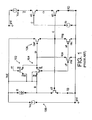
- Fig. 1 is a schematic diagram of one exemplary prior art circuit 100 that generates one unit (e.g., 10mA) of the current pulse. Because the NPN devices are biased near their peak cutoff frequency (F t ), the base emitter voltage (V be ) of the transistors are approximately 1V (volt). Therefore, the base of the emitter follower transistor Q sf 106 is approximately 2V. If NMOS 102 and PMOS 104 switches are used to switch the base of the emitter follower transistor Q sf between "on” and “off” states, the voltage swing for the gates of the NMOS and PMOS switches 102 and 104 are very large (approximately 2.7V). The large voltage swing dissipates more power than desired.
- F t peak cutoff frequency
- a large switch provides the required reduction in the DC drop; however, a large transient power is also required.
- the present example solves the foregoing problems by, inter alia, utilizing a dummy MOS transistor Switch (MSW).
- MSW dummy MOS transistor Switch
- the dummy switch in the exemplary embodiments is chosen to be comparatively small (including having a low switching power) since multiple of such switches may be used in the output stage of a given device.
- Fig. 2 is a diagram of an exemplary DAC circuit 200 which functions as a controlled current source.
- Circuit 200 may itself form a single bit DAC and receive at its input(s) a single bit of digital information and output a current level corresponding to the value of the binary bit input.
- a plurality of circuits 200 may be utilized in a multi-bit DAC to convert a multi-bit digital signal into an analog signal.
- the use of controlled current sources in multi-bit DACs is known in the art and will not be described in detail for reasons of simplicity.
- circuit 200 is adapted to switch the base of the output transistor qD to either a reference bias voltage, set by the reference branch circuit 201 including transistors Qsf and qB, or to ground.
- a low voltage e.g., 1.7V
- Circuit 200 further includes a load branch circuit 202, including transistor qD.
- the base of the emitter follower transistor Q sf is still at approximately 2V, yet it is not switched, but rather just a dc bias voltage.
- reference branch circuit 201 is shared with a plurality of other load branch circuits 202 within the output section of the present DAC (e.g., approximately 100 other output sections in the exemplary embodiment), the current and power dissipation in the reference branch circuit 201 is insignificant.
- transistor MSN MSW
- transistor Mpd When transistor MSN (MSW) is activated or turned on and transistor Mpd is turned off, reference branch circuit 201 and the load branch circuit(s) 202 form a current mirror, in which the reference current that flows through transistor qD in the load branch circuit 202 is proportional to (or mirrors) the current in reference branch circuit 201.
- transistor MSN is turned off and transistor Mpd is turned on, transistor qD is turned off and no current flows in load branch 202
- the drain-to-source resistance of transistor MSN (MSW) in circuit 200 causes a nonzero DC voltage drop across MSW, which results in a mismatch of the current between the reference branch circuit 201 and load branch circuit 202.
- MSW transistor MSN
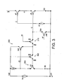
- Fig. 3 is a circuit diagram of one example.
- a "dummy" switch 302 is placed between the base terminal of transistor 304 (qB) and MSW 310.
- This dummy switch device 302 is selected so as to comprise a fraction (e.g., 1/20 th ) of the width (current) of the main switch device MSN 310.
- Dummy switch 302 corrects for the DC voltage drop created by transistor 301 so as to allow for the current in load branch circuit 202 relatively closely follows (mirrors) the current in reference branch circuit 201.
- Figs. 4a and 4b are graphs that illustrate exemplary SPICE simulation results for circuits with and without a dummy switch, respectively.
- a current pulse with a fast rising edge is desired from a controlled current source circuit(s) in an RDAC.
- One method of achieving this sharp rising edge is to use an emitter follower to pull up the base node of the device qD.
- MOS switch(s) e.g., NMOS and PMOS switches
- MOS switch(s) e.g., NMOS and PMOS switches
- Fig. 5 is a schematic of one such exemplary controlled current source for an RDAC according to the invention.
- a capacitor 502 (C boost ) is used to capacitively couple the high speed input control signal "on" 504 to the base node “G” 506 of the output transistor qD 508.
- Both the MOS transistor switches MSN, MSP and the C boost capacitor 502 are scaled to as small a value as possible, while still providing the desired boost in the rising edge of the current pulse.
- the actual switches are, in the illustrated embodiment, parallel combinations of NMOS and PMOS transistors, although other arrangements may conceivably be used. This configuration cancels the clock and charge, as well as providing lower resistance and voltage drop across the switches.
- Fig. 6a shows a graph of the output current of an exemplary circuit (simulated) without the C boost capacitor of Fig. 5 .
- Fig. 6b shows a graph of the output current of the same circuit with the C boost capacitor 502. With the capacitor, the edges of the current pulse advantageously rise and fall much more quickly than without the capacitor, as shown in Figs. 6b and 6a , respectively.
- the base of the output transistor device qD (see prior discussion) is switched to ground, or to approximately the base voltage of the reference bias device qB, depending upon the state of the "on" and "off” input signals.
- This causes a fairly large base voltage swing for qD (typically on the order of 1V). Since the output device qD is comparatively large with large input capacitance, this larger base voltage swing is slower, and consumes more power than is optimal.
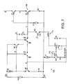
- Fig. 7 is a circuit diagram of an example of a controlled current source circuit 700 adapted to reduce the aforementioned base voltage swing of output transistor qD.
- the base node of transistor 708 (qD) of the circuit 700 of Fig. 7 is switched to a bias rail voltage of gndG 710 that is greater than the ground potential.
- This gndG voltage rail is generated by using a transistor 712 (qd0) of the same type and substantially the same size as the output transistor 708. It will be appreciated that while the present embodiment uses devices 712, 708 that are substantially identical in size, some degree of variation in sizing and/or configuration between the two devices can be tolerated, subject to the limitations described below.
- a very small current is used to bias the transistor 712 to a state wherein the transistor 712 is barely “ON” (e.g., 10 ⁇ A in the exemplary embodiment, wherein the normal "ON” state is on the order of 10 mA, three orders of magnitude higher).
- the base voltage of transistor 712 may be buffered.
- the ground rail “gndG” is used to pull the transistor 712 to the “OFF” state, thereby drastically reducing the voltage swing of the base node (G) of output transistor 708, and achieving significantly faster speeds with reduced power dissipation.
- the device qDo 712 is the same size and configuration as the real output transistor qD 708, the base voltage bias rail that is set up to turn the device qD 708 to the aforementioned "barely ON" state will advantageously track process, temperature and power supply changes, thereby avoiding differentials and unpredictable effects.
- Fig. 8a compares the base voltage of transistor 708 (node G) with and without its coupling to the bias rail gndG 710 of the configuration of Fig. 7 .
- Fig. 8b compares the base current of transistor 708 with the bias rail (see trace 804) and without the bias rail gndG 710.
- both Figs. 8a and 8b show a marked improvement on the speed of the current pulse when the bias rail approach of Fig. 7 is used.
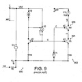
- Fig. 9 shows a circuit diagram of a typical prior art output circuit 900 (generally for similar uses as those of Figs. 2 , 3 , 5 and 7 previously discussed herein).
- the output circuit stage 902 comprises a high speed (HS) transistor 904 and a high voltage (HV) transistor 906 coupled in a cascade configuration.
- HS high speed
- HV high voltage
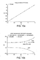
- Fig. 10a shows a plot of the output voltage of output circuit stage 902 (node "out", voltage at the collector of the HV device 906).
- the collector current of a high voltage device 906 at a lower values of collector voltage (vo) is about 10mA.
- the collector current increased to approximately 19mA.
- This avalanche multiplication current flows out through the base node as shown in the plot IS(qC/B) 1002 in Fig. 10b .
- the present disclosure provides three (3) exemplary alternative circuit configurations adapted to compensate for the foregoing avalanche multiplication current; see Figs. 11a , 11b , and 11c .
- the base current of HV in each circuit of Figs. 11a , 11b , and 11c is sensed by a voltage source vma, vmb, and vmc, respectively. These base currents are then injected into the collector, emitter and reference bias, respectively, of the HV device 1104 (corresponding to the device 906 of the prior art configuration of Fig. 9 .) to compensate for the avalanche multiplication current.
- the uncompensated collector current IS(qC/C) 1004 increase from 10mA to 19mA ( Fig. 10b).
- Fig. 10b also shows the uncompensated base current (qC/B) 1002 of HV increasing (in magnitude) from 0mA to 9mA.
- the compensated currents 1008, 1010, 1012 associated with each circuit of Figs. 11a , 11b , and 11c advantageously remains very flat at 10mA for an output voltage swing from 2V to 14V.
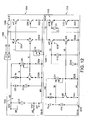
- sub-circuit A (Sub#A) 1202 is the main output circuit, comparable to that of Fig. 11c .
- the collector of the high voltage device1204 is connected to output node O p 1206.
- Output node O p may have a sinusoidal voltage swing from approximately 2V to approximately 14V as shown in Fig. 13a .
- Sub-circuit (Sub#B) 1210 comprises a base current sensing circuit for sub-circuit A (Sub#A).
- the third sub-circuit (Sub#C) 1214 is optional; it is used to subtract and exclude the capacitive current component due to the sinusoidal output voltage swing of sub-circuit 1204.
- Sub-circuit (Sub#C) 1214 may also be used for simulation and testing.
- the fourth sub-circuit (Sub#D) 1218 is also optional, but may be used as an additional feature of the circuit.
- the transistor 1220 monitors the output voltage O p (Sub#D) to generate the avalanche multiplication current.
- the current generated by the transistor 1220 comprises a first component due to avalanche multiplication, and a second component due to the capacitive coupling. This second component is an undesirable capacitive current injected into the compensation circuit by the sinusoidal output voltage swing.
- the illustrated circuit 1200 utilizes transistor 1222, which is used to sense only the capacitive current (second) component due to the sinusoidal output voltage swing. This capacitive current is subtracted from current generated by transistor 1220. Thus, the net result is only the avalanche multiplication current, which is then used by the first sub-circuit (Sub#A) 1202 via the connection 1226 between the circuits to compensate the relatively high output voltage of transistor 1204.
- Fig. 13a shows the sinusoidal output voltage (O p ) swing from 2V to 14V (peak-to-peak).
- Fig. 13b shows the output current from the high voltage transistor 1204, which advantageously remains relatively constant near 10mA.
- FIG. 14 and 14a an exemplary radio frequency transceiver system utilizing the improved converter of the present invention is described.
- the transceiver 1400 comprises a baseband processor 1402, a fractional interpolator 1404 (such as that described in co-pending and co-owned U.S. Patent entitled “NOISE SHAPED INTERPOLATOR AND DECIMATOR APPARATUS AND METHOD”), noise shaping coder (NSC) 1410, sample and hold interpolator 1412, a digital I/Q quadrature mixer and combiner 1413, and a high-efficiency DAC 1414 such as that described above.
- a resonator (not shown) is also utilized in conjunction with the duplexer 1416 to generate the analog output of the transmitter. As described in detail in co-owned and co-pending U.S. Patent Application No.
- the interpolator, NSC, DAC and resonator cooperate to convert the digital in-phase (I) and quadrature (Q) signals obtained from the baseband processor directly to an analog representation at carrier frequency for transmission over an antenna in a highly power-efficient manner.
- the transmitter is further adapted to dislocate quantization noise generated by the transmitter outside of one or more receive bands associated with a related receiver unit of the transmitter.
- Prior art transmitters typically comprise baseband symbols (I and Q) being converted from digital to analog by a DAC operating at a baseband frequency, f b , or a small integer multiple of f b , e.g., 4f b or 8f b . From that point onward in the signal path, the processing is typically in the analog domain, including the up-conversion process.
- the baseband symbols are digitally interpolated up to a sample rate at or substantially near the desired frequency, and then encoded.
- the encoding method may be performed by a delta-sigma modulator or noise-shaping coder.
- the output of the coder is represented by a coarsely quantized signal of one or more bits by an RDAC.
- the output of the RDAC is coupled to a bandpass filter or resonator, which is part of the duplexer in the exemplary embodiment of Fig. 14 .
- a DC/DC converter (see Fig. 14a ) may be used to control the bias level of the RDAC dynamically to improve power efficiency.
- One such way is described in the co-pending U.S.
- Fig. 14a provides a greater level of detail of the RDAC portion of the circuit 1400 of Fig. 14 .
- Figure 14a is comprised of the subcircuit 1420, which is comprised of Interpolator 1412, I/Q digital mixer and combiner 1413, and DAC 1414.
- a ternary ⁇ -1, 0, +1 ⁇ quantization encoder is used in conjunction with a plurality of DACs which substitute for a single DAC.
- each individual current source and corresponding switch in Fig. 14a which forms a single 'finger' or component of a larger current source as shown in the Fig. 14a , may be implemented as a controlled current source of Figs. 2 , 3 , 5 , 7 , 11a-c or 12 .
- This approach has the benefit of, inter alia, facilitating power control. Additional detail on the operation of this circuit is provided in the 10/382,297 application referenced above.
- Fig. 14a includes a DAC having a unary weighted architecture and utilizing a plurality of the controlled current sources of the type shown in Figs. 2 , 3 , 5 , 7 , 11a-c , and 12 , it is understood that the controlled current source circuits of the present invention may be used in other DAC architectures, such as binary weighted DACs and segmented DACs.
- controlled current sources of Figs. 2 , 3 , 5 , 7 , 11a-c and 12 may be implemented with other types of transistors.
- the transmitter comprises a traditional carrier-based architecture having a baseband processor, DAC, up-conversion apparatus (from baseband to an intermediate frequency and then to carrier), power amplifier, and antenna.
- the DAC operates to receive digital I and Q signals from the baseband processor, and convert these signals to the analog domain for subsequent up-conversion, power amplification, and transmission over the antenna. Note that the higher speed and lower resolution of the embodiment of Figs. 14 and 14a can be traded off for a more traditional functionality (i.e., lower speed and higher resolution) through proper adaptation of the circuit described previously herein.
- Figure 14 includes a receiver, subcircuit 1442, as well as a transmitter 1441.
- the receiver includes an ADC (analog-to-digital converter) function, which may include one or more elements or embodiments of the RDAC as described in the present invention disclosure.
- ADC's may include DAC's as part of the overall ADC function. Therefore, the virtues of the present invention can readily apply to a receiver and/or ADC, including without limitation delta-sigma and "flash" type ADCs.
- the various circuits of the present invention may be rendered as stand-alone or discrete electronic circuits, as well as integrated circuit (IC) devices.
- integrated circuit devices may include, for example, system-on-chip (SoC) devices which integrate multiple functions or modules onto a single semiconductive die rendered in a sub-micron SiGe process.
- SoC system-on-chip
- the RDAC circuits are included with the digitally switched resonator, noise shaping coder, etc. of the direct-conversion architecture referenced above.
- Baseband processing may also optionally be included within this device.
- This highly integrated approach provides significant benefits in terms of size and compactness, power consumption, and ease of design and implementation. It also leverages one of the primary benefits of the exemplary direct-conversion architecture described above; i.e., simplification and obviation of many prior art RF amplifier and up-conversion/downconversion components which would otherwise be provided as discrete devices.
Landscapes
- Engineering & Computer Science (AREA)
- Power Engineering (AREA)
- Theoretical Computer Science (AREA)
- Amplifiers (AREA)
- Superheterodyne Receivers (AREA)
Claims (5)
- Digital/Analog-Umsetzer (100), der angepasst ist, verbesserte Leistung der Anstiegsflanke für Stromimpulse bereitzustellen, umfassend:einen Referenz-Abzweigstromkreis, der Transistoren (IB, 9B, QsF) einschließt;einen Verbraucherabzweigstromkreis, der zumindest einen Ausgangstransistor (508) einschließt;einen ersten Schalter mit einer ersten Breite, wobei der besagte erste Schalter durch Empfangen eines Hochgeschwindigkeitssteuersignals(504) gesteuert wird, das angepasst ist, eine Basis (qD) des besagten zumindest einen Ausgangstransistors (508) auf eine einer Vielheit von Spannungen zu schalten, die vom Referenz-Abzweigstromkreis generiert wurden; wobei, wenn der besagte erste Schalter aktiviert wird, der besagte Referenz-Abzweigstromkreis und der besagte Verbraucherabzweigstromkreis einen Stromspiegel bilden;einen zweiten Schalter, der elektrisch zwischen dem besagten ersten Schalter und einem ersten der besagten Transistoren im besagten Referenz-Abzweigstromkreis gekoppelt ist, besagter zweite Schalter eine zweite Breite hat, wobei die besagte zweite Breite ein Bruchteil der besagten ersten Breite des besagten ersten Schalters ist, derart, dass der besagte zweite Schalter angepasst ist, einen Spannungsabfall zu berichtigen, der mit dem besagten ersten Schalter assoziiert ist; undzumindest einen Kondensator (502), der elektrisch zwischen dem Hochgeschwindigkeits-Steuersignalknoten (504) und der Basis (qD) des besagten zumindest einen Ausgangstransistors (508) angeordnet ist;wobei der zumindest eine Ausgangstransistor (508), der die besagten Stromimpulse generiert und der besagte zumindest eine Kondensator (502) konfiguriert ist, eine Anstiegsflanke der besagten Stromimpulse nach Empfangen eines Hochgeschwindigkeitssteuersignals zum besagten Hochgeschwindigkeitssteuersignal (504) zu verstärken.
- Digital/Analog-Umsetzer nach Anspruch 1, wobei zumindest einer der besagten ersten und zweiten Schalter parallele Kombinationen von NMOS- und PMOS-Halbleitern umfasst.
- Hochfrequenzsender, umfassend:einen Basisbandprozessor, der fähig ist, digitale Daten zu verarbeiten und zumindest eine Ausgabe zu produzieren, die verarbeitete Digitaldaten umfasst;und der Digital/Analog-Umsetzer wie in Anspruch 1 beansprucht, wobei der besagte Digital/Analog-Umsetzer angepasst ist, die besagten verarbeiteten Digitaldaten als das Hochleistungssteuersignal zu empfangen und es in den Stromimpuls umzusetzen;eine Antenne, die angepasst ist, zumindest einen Teil der besagten Stromimpulse zu senden.
- Sender nach Anspruch 3, der weiter eine rauschgeformte Codiervorrichtung umfasst, die wirkend mit dem besagten Digital/Analog-Umsetzer kommuniziert.
- Sender nach Anspruch 3 oder 4, der weiter einen Resonator umfasst, der wirkend an den besagten Digital/Analog-Umsetzer gekoppelt ist.
Priority Applications (1)
| Application Number | Priority Date | Filing Date | Title |
|---|---|---|---|
| EP10184145A EP2270984A1 (de) | 2003-08-05 | 2004-08-04 | Verbesserter Hochfrequenz-Digital/Analog - Umsetzer |
Applications Claiming Priority (3)
| Application Number | Priority Date | Filing Date | Title |
|---|---|---|---|
| US49305203P | 2003-08-05 | 2003-08-05 | |
| US10/910,917 US7116253B2 (en) | 2003-08-05 | 2004-08-03 | Radio frequency digital-to-analog converter |
| PCT/US2004/025324 WO2005015753A2 (en) | 2003-08-05 | 2004-08-04 | Improved radio frequency digital-to-analog converter |
Related Child Applications (1)
| Application Number | Title | Priority Date | Filing Date |
|---|---|---|---|
| EP10184145.0 Division-Into | 2010-09-30 |
Publications (3)
| Publication Number | Publication Date |
|---|---|
| EP1869769A4 EP1869769A4 (de) | 2007-12-26 |
| EP1869769A2 EP1869769A2 (de) | 2007-12-26 |
| EP1869769B1 true EP1869769B1 (de) | 2013-05-01 |
Family
ID=34798716
Family Applications (2)
| Application Number | Title | Priority Date | Filing Date |
|---|---|---|---|
| EP04786460.8A Expired - Lifetime EP1869769B1 (de) | 2003-08-05 | 2004-08-04 | Verbesserter hochfrequenz-digital/analog-umsetzer |
| EP10184145A Withdrawn EP2270984A1 (de) | 2003-08-05 | 2004-08-04 | Verbesserter Hochfrequenz-Digital/Analog - Umsetzer |
Family Applications After (1)
| Application Number | Title | Priority Date | Filing Date |
|---|---|---|---|
| EP10184145A Withdrawn EP2270984A1 (de) | 2003-08-05 | 2004-08-04 | Verbesserter Hochfrequenz-Digital/Analog - Umsetzer |
Country Status (3)
| Country | Link |
|---|---|
| US (2) | US7116253B2 (de) |
| EP (2) | EP1869769B1 (de) |
| WO (1) | WO2005015753A2 (de) |
Families Citing this family (15)
| Publication number | Priority date | Publication date | Assignee | Title |
|---|---|---|---|---|
| US7426372B2 (en) * | 2005-03-31 | 2008-09-16 | M/A-Com Eurotec B.V. | Piecewise linearizer circuit for radio frequency amplification |
| US7348847B2 (en) * | 2005-04-28 | 2008-03-25 | Sige Semiconductor Inc. | Integrated implementation of a collector boost scheme and method therefor |
| US7183956B1 (en) * | 2005-08-10 | 2007-02-27 | Northrop Grumman Corporation | High speed digital delta-sigma modulator with integrated upsampler |
| US7345612B2 (en) * | 2006-02-07 | 2008-03-18 | Nokia Corporation | Digital-to-radio frequency conversion device, chip set, transmitter, user terminal and data processing method |
| JP2009535864A (ja) * | 2006-02-21 | 2009-10-01 | エヌエックスピー ビー ヴィ | 指数デジタル−アナログ変換器 |
| US7504976B1 (en) * | 2007-01-31 | 2009-03-17 | Lockheed Martin Corporation | Direct radio frequency generation using power digital-to-analog conversion |
| US8045670B2 (en) * | 2007-06-22 | 2011-10-25 | Texas Instruments Incorporated | Interpolative all-digital phase locked loop |
| EP2037584A1 (de) | 2007-09-14 | 2009-03-18 | STMicroelectronics N.V. | Verfahren zur Durchführung einer Digital-Analog-Wandlung eines digitalen Signals und entsprechende elektronische Vorrichtung |
| EP3678294B1 (de) | 2007-09-14 | 2022-02-02 | Telefonaktiebolaget LM Ericsson (publ) | Verfahren zur notch-filtration eines digitalen signals und zugehörige elektronische vorrichtung |
| US7884747B2 (en) * | 2009-06-12 | 2011-02-08 | Analog Devices, Inc. | Digital to analog converters having circuit architectures to overcome switch losses |
| US8401600B1 (en) | 2010-08-02 | 2013-03-19 | Hypres, Inc. | Superconducting multi-bit digital mixer |
| US8494086B2 (en) * | 2011-01-14 | 2013-07-23 | Broadcom Corporation | Distortion and aliasing reduction for digital to analog conversion |
| US9083376B2 (en) * | 2013-04-25 | 2015-07-14 | Maxlinear, Inc. | Successive approximation register analog-to-digital converter |
| WO2016164018A1 (en) * | 2015-04-09 | 2016-10-13 | Entropic Communications, Inc. | Dac with envelope controlled bias |
| TWI886686B (zh) | 2023-12-13 | 2025-06-11 | 財團法人工業技術研究院 | 數位類比轉換器及其操作方法 |
Citations (1)
| Publication number | Priority date | Publication date | Assignee | Title |
|---|---|---|---|---|
| US4539493A (en) * | 1983-11-09 | 1985-09-03 | Advanced Micro Devices, Inc. | Dynamic ECL circuit adapted to drive loads having significant capacitance |
Family Cites Families (17)
| Publication number | Priority date | Publication date | Assignee | Title |
|---|---|---|---|---|
| JPS57178420A (en) * | 1981-04-25 | 1982-11-02 | Toshiba Corp | D/a converter |
| US4709167A (en) * | 1982-08-16 | 1987-11-24 | Analog Devices, Inc. | Three-state output buffer with anti-saturation control |
| US4607249A (en) * | 1985-05-08 | 1986-08-19 | Bbrr-Brown Corporation | Input level shifting circuit for low voltage digital-to-analog converter |
| JPH01261024A (ja) * | 1988-04-12 | 1989-10-18 | Hitachi Ltd | 論理回路 |
| JP2518068B2 (ja) * | 1989-11-17 | 1996-07-24 | 日本電気株式会社 | 電流切換回路 |
| US5245254A (en) * | 1992-07-15 | 1993-09-14 | Gold Star Co., Ltd. | Horizontal focus circuit in an image display |
| US5483150A (en) * | 1993-02-05 | 1996-01-09 | Hughes Aircraft Company | Transistor current switch array for digital-to-analog converter (DAC) including bias current compensation for individual transistor current gain and thermally induced base-emitter voltage drop variation |
| US5373294A (en) * | 1993-07-12 | 1994-12-13 | Nec Electronics, Inc. | Current switch for a high speed DAC |
| US5508702A (en) * | 1994-06-17 | 1996-04-16 | National Semiconductor Corp. | BiCOMS digital-to-analog conversion |
| US5625360A (en) * | 1995-09-05 | 1997-04-29 | Motorola, Inc. | Current source for reducing noise glitches generated in a digital to analog converter and method therefor |
| US5838192A (en) * | 1996-01-17 | 1998-11-17 | Analog Devices, Inc. | Junction field effect voltage reference |
| US5789974A (en) * | 1996-07-17 | 1998-08-04 | Analog Devices, Inc. | Calibrating the DC-offset of amplifiers |
| US5914621A (en) * | 1998-02-05 | 1999-06-22 | Applied Micro Circuits Corporation | Charge balanced ramp with improved signal linearity |
| FR2798791B1 (fr) * | 1999-09-17 | 2001-12-07 | Thomson Csf | Convertisseur numerique-analogique en courant |
| JP3628587B2 (ja) * | 2000-04-24 | 2005-03-16 | シャープ株式会社 | 電流スイッチ回路およびそれを用いるd/aコンバータ |
| US6426614B1 (en) * | 2000-08-24 | 2002-07-30 | Research In Motion Limited | Boot-strapped current switch |
| US6486816B2 (en) * | 2001-04-03 | 2002-11-26 | Texas Instruments Incorporated | CDAC operation at low supply voltages |
-
2004
- 2004-08-03 US US10/910,917 patent/US7116253B2/en not_active Expired - Lifetime
- 2004-08-04 EP EP04786460.8A patent/EP1869769B1/de not_active Expired - Lifetime
- 2004-08-04 WO PCT/US2004/025324 patent/WO2005015753A2/en not_active Ceased
- 2004-08-04 EP EP10184145A patent/EP2270984A1/de not_active Withdrawn
-
2006
- 2006-06-13 US US11/452,183 patent/US7471226B2/en not_active Expired - Lifetime
Patent Citations (1)
| Publication number | Priority date | Publication date | Assignee | Title |
|---|---|---|---|---|
| US4539493A (en) * | 1983-11-09 | 1985-09-03 | Advanced Micro Devices, Inc. | Dynamic ECL circuit adapted to drive loads having significant capacitance |
Also Published As
| Publication number | Publication date |
|---|---|
| EP2270984A1 (de) | 2011-01-05 |
| US20050162294A1 (en) | 2005-07-28 |
| US7471226B2 (en) | 2008-12-30 |
| EP1869769A4 (de) | 2007-12-26 |
| EP1869769A2 (de) | 2007-12-26 |
| US7116253B2 (en) | 2006-10-03 |
| WO2005015753A3 (en) | 2006-01-26 |
| US20060244648A1 (en) | 2006-11-02 |
| WO2005015753A2 (en) | 2005-02-17 |
Similar Documents
| Publication | Publication Date | Title |
|---|---|---|
| US7116253B2 (en) | Radio frequency digital-to-analog converter | |
| KR101433484B1 (ko) | 저전력, 저잡음 디지털-아날로그 컨버터 기준 회로 | |
| US8237499B2 (en) | Feedforward controlled envelope modulator and feedforward control circuit thereof | |
| JP3039809B2 (ja) | アナログ/ディジタル変換器、サンプリングパルス生成回路、及び電流スイッチ回路 | |
| US20250149136A1 (en) | Ultra wideband (uwb) transmitter and receiver circuits | |
| US7154329B2 (en) | Method and apparatus for compensating amplifier output for temperature and process variations | |
| Juanda et al. | A 10-GS/s 4-bit single-core digital-to-analog converter for cognitive ultrawidebands | |
| WO2006036900A1 (en) | High-speed and high-accuracy digital-to-analog converter | |
| US7463869B2 (en) | Low noise high isolation transmit buffer gain control mechanism | |
| EP2932596B1 (de) | Analoges basisbandfilter für funksendeempfänger | |
| Kim et al. | A 12-b, 1-GS/s 6.1 mW current-steering DAC in 14 nm FinFET with 80 dB SFDR for 2G/3G/4G cellular application | |
| US8324967B2 (en) | System and method for controlling a power amplifier using a programmable ramp circuit | |
| Zimmermann et al. | Design of an RF-DAC in 65nm CMOS for multistandard, multimode transmitters | |
| US20090295613A1 (en) | Performing analog-to-digital conversion by computing delay time between traveling waves in transmission lines | |
| Tan et al. | Design and implementation of high-performance CMOS D/A converter | |
| Chien et al. | Ultra-low-voltage CMOS static frequency divider | |
| Weiß et al. | A novel 32-Gb/s 5.6-vpp Digital-to-Analog converter in 100 nm GaN technology for 5G signal generation | |
| Weiß | Realization of Radio Frequency Digital-to-Analog Converters in Gallium Nitride Technology for 5G Mobile Communication | |
| Bol et al. | An 802.15. 4 IR-UWB transmitter SoC with adaptive-FBB-based channel selection and programmable pulse shape | |
| Cho et al. | Introduction to the Special Issue on the 2010 IEEE International Solid-State Circuits Conference | |
| Park et al. | A Current Mode 10bit 1GHz CMOS D/A Converter | |
| Papananos et al. | Mixed analog-digital pulse-width modulator for massive-MIMO transmitters |
Legal Events
| Date | Code | Title | Description |
|---|---|---|---|
| PUAI | Public reference made under article 153(3) epc to a published international application that has entered the european phase |
Free format text: ORIGINAL CODE: 0009012 |
|
| 17P | Request for examination filed |
Effective date: 20060306 |
|
| A4 | Supplementary search report drawn up and despatched |
Effective date: 20071123 |
|
| AK | Designated contracting states |
Kind code of ref document: A2 Designated state(s): AT BE BG CH CY CZ DE DK EE ES FI FR GB GR HU IE IT LI LU MC NL PL PT RO SE SI SK TR |
|
| 17Q | First examination report despatched |
Effective date: 20080423 |
|
| GRAP | Despatch of communication of intention to grant a patent |
Free format text: ORIGINAL CODE: EPIDOSNIGR1 |
|
| GRAS | Grant fee paid |
Free format text: ORIGINAL CODE: EPIDOSNIGR3 |
|
| GRAA | (expected) grant |
Free format text: ORIGINAL CODE: 0009210 |
|
| AK | Designated contracting states |
Kind code of ref document: B1 Designated state(s): AT BE BG CH CY CZ DE DK EE ES FI FR GB GR HU IE IT LI LU MC NL PL PT RO SE SI SK TR |
|
| REG | Reference to a national code |
Ref country code: GB Ref legal event code: FG4D |
|
| REG | Reference to a national code |
Ref country code: CH Ref legal event code: EP Ref country code: AT Ref legal event code: REF Ref document number: 610465 Country of ref document: AT Kind code of ref document: T Effective date: 20130515 |
|
| REG | Reference to a national code |
Ref country code: IE Ref legal event code: FG4D |
|
| REG | Reference to a national code |
Ref country code: DE Ref legal event code: R096 Ref document number: 602004041992 Country of ref document: DE Effective date: 20130704 |
|
| REG | Reference to a national code |
Ref country code: AT Ref legal event code: MK05 Ref document number: 610465 Country of ref document: AT Kind code of ref document: T Effective date: 20130501 |
|
| REG | Reference to a national code |
Ref country code: NL Ref legal event code: VDEP Effective date: 20130501 |
|
| PG25 | Lapsed in a contracting state [announced via postgrant information from national office to epo] |
Ref country code: GR Free format text: LAPSE BECAUSE OF FAILURE TO SUBMIT A TRANSLATION OF THE DESCRIPTION OR TO PAY THE FEE WITHIN THE PRESCRIBED TIME-LIMIT Effective date: 20130802 Ref country code: FI Free format text: LAPSE BECAUSE OF FAILURE TO SUBMIT A TRANSLATION OF THE DESCRIPTION OR TO PAY THE FEE WITHIN THE PRESCRIBED TIME-LIMIT Effective date: 20130501 Ref country code: SI Free format text: LAPSE BECAUSE OF FAILURE TO SUBMIT A TRANSLATION OF THE DESCRIPTION OR TO PAY THE FEE WITHIN THE PRESCRIBED TIME-LIMIT Effective date: 20130501 Ref country code: SE Free format text: LAPSE BECAUSE OF FAILURE TO SUBMIT A TRANSLATION OF THE DESCRIPTION OR TO PAY THE FEE WITHIN THE PRESCRIBED TIME-LIMIT Effective date: 20130501 Ref country code: AT Free format text: LAPSE BECAUSE OF FAILURE TO SUBMIT A TRANSLATION OF THE DESCRIPTION OR TO PAY THE FEE WITHIN THE PRESCRIBED TIME-LIMIT Effective date: 20130501 Ref country code: ES Free format text: LAPSE BECAUSE OF FAILURE TO SUBMIT A TRANSLATION OF THE DESCRIPTION OR TO PAY THE FEE WITHIN THE PRESCRIBED TIME-LIMIT Effective date: 20130812 Ref country code: PT Free format text: LAPSE BECAUSE OF FAILURE TO SUBMIT A TRANSLATION OF THE DESCRIPTION OR TO PAY THE FEE WITHIN THE PRESCRIBED TIME-LIMIT Effective date: 20130902 |
|
| PG25 | Lapsed in a contracting state [announced via postgrant information from national office to epo] |
Ref country code: BG Free format text: LAPSE BECAUSE OF FAILURE TO SUBMIT A TRANSLATION OF THE DESCRIPTION OR TO PAY THE FEE WITHIN THE PRESCRIBED TIME-LIMIT Effective date: 20130801 Ref country code: CY Free format text: LAPSE BECAUSE OF FAILURE TO SUBMIT A TRANSLATION OF THE DESCRIPTION OR TO PAY THE FEE WITHIN THE PRESCRIBED TIME-LIMIT Effective date: 20130501 Ref country code: PL Free format text: LAPSE BECAUSE OF FAILURE TO SUBMIT A TRANSLATION OF THE DESCRIPTION OR TO PAY THE FEE WITHIN THE PRESCRIBED TIME-LIMIT Effective date: 20130501 |
|
| PG25 | Lapsed in a contracting state [announced via postgrant information from national office to epo] |
Ref country code: SK Free format text: LAPSE BECAUSE OF FAILURE TO SUBMIT A TRANSLATION OF THE DESCRIPTION OR TO PAY THE FEE WITHIN THE PRESCRIBED TIME-LIMIT Effective date: 20130501 Ref country code: CZ Free format text: LAPSE BECAUSE OF FAILURE TO SUBMIT A TRANSLATION OF THE DESCRIPTION OR TO PAY THE FEE WITHIN THE PRESCRIBED TIME-LIMIT Effective date: 20130501 Ref country code: EE Free format text: LAPSE BECAUSE OF FAILURE TO SUBMIT A TRANSLATION OF THE DESCRIPTION OR TO PAY THE FEE WITHIN THE PRESCRIBED TIME-LIMIT Effective date: 20130501 Ref country code: BE Free format text: LAPSE BECAUSE OF FAILURE TO SUBMIT A TRANSLATION OF THE DESCRIPTION OR TO PAY THE FEE WITHIN THE PRESCRIBED TIME-LIMIT Effective date: 20130501 Ref country code: DK Free format text: LAPSE BECAUSE OF FAILURE TO SUBMIT A TRANSLATION OF THE DESCRIPTION OR TO PAY THE FEE WITHIN THE PRESCRIBED TIME-LIMIT Effective date: 20130501 |
|
| PG25 | Lapsed in a contracting state [announced via postgrant information from national office to epo] |
Ref country code: IT Free format text: LAPSE BECAUSE OF FAILURE TO SUBMIT A TRANSLATION OF THE DESCRIPTION OR TO PAY THE FEE WITHIN THE PRESCRIBED TIME-LIMIT Effective date: 20130501 Ref country code: NL Free format text: LAPSE BECAUSE OF FAILURE TO SUBMIT A TRANSLATION OF THE DESCRIPTION OR TO PAY THE FEE WITHIN THE PRESCRIBED TIME-LIMIT Effective date: 20130501 Ref country code: RO Free format text: LAPSE BECAUSE OF FAILURE TO SUBMIT A TRANSLATION OF THE DESCRIPTION OR TO PAY THE FEE WITHIN THE PRESCRIBED TIME-LIMIT Effective date: 20130501 |
|
| PLBE | No opposition filed within time limit |
Free format text: ORIGINAL CODE: 0009261 |
|
| STAA | Information on the status of an ep patent application or granted ep patent |
Free format text: STATUS: NO OPPOSITION FILED WITHIN TIME LIMIT |
|
| REG | Reference to a national code |
Ref country code: CH Ref legal event code: PL |
|
| 26N | No opposition filed |
Effective date: 20140204 |
|
| GBPC | Gb: european patent ceased through non-payment of renewal fee |
Effective date: 20130804 |
|
| PG25 | Lapsed in a contracting state [announced via postgrant information from national office to epo] |
Ref country code: LI Free format text: LAPSE BECAUSE OF NON-PAYMENT OF DUE FEES Effective date: 20130831 Ref country code: CH Free format text: LAPSE BECAUSE OF NON-PAYMENT OF DUE FEES Effective date: 20130831 Ref country code: MC Free format text: LAPSE BECAUSE OF FAILURE TO SUBMIT A TRANSLATION OF THE DESCRIPTION OR TO PAY THE FEE WITHIN THE PRESCRIBED TIME-LIMIT Effective date: 20130501 |
|
| REG | Reference to a national code |
Ref country code: DE Ref legal event code: R097 Ref document number: 602004041992 Country of ref document: DE Effective date: 20140204 |
|
| REG | Reference to a national code |
Ref country code: IE Ref legal event code: MM4A |
|
| PG25 | Lapsed in a contracting state [announced via postgrant information from national office to epo] |
Ref country code: IE Free format text: LAPSE BECAUSE OF NON-PAYMENT OF DUE FEES Effective date: 20130804 Ref country code: GB Free format text: LAPSE BECAUSE OF NON-PAYMENT OF DUE FEES Effective date: 20130804 |
|
| PG25 | Lapsed in a contracting state [announced via postgrant information from national office to epo] |
Ref country code: TR Free format text: LAPSE BECAUSE OF FAILURE TO SUBMIT A TRANSLATION OF THE DESCRIPTION OR TO PAY THE FEE WITHIN THE PRESCRIBED TIME-LIMIT Effective date: 20130501 |
|
| PG25 | Lapsed in a contracting state [announced via postgrant information from national office to epo] |
Ref country code: HU Free format text: LAPSE BECAUSE OF FAILURE TO SUBMIT A TRANSLATION OF THE DESCRIPTION OR TO PAY THE FEE WITHIN THE PRESCRIBED TIME-LIMIT; INVALID AB INITIO Effective date: 20040804 Ref country code: LU Free format text: LAPSE BECAUSE OF NON-PAYMENT OF DUE FEES Effective date: 20130804 |
|
| REG | Reference to a national code |
Ref country code: FR Ref legal event code: PLFP Year of fee payment: 13 |
|
| REG | Reference to a national code |
Ref country code: FR Ref legal event code: PLFP Year of fee payment: 14 |
|
| REG | Reference to a national code |
Ref country code: FR Ref legal event code: PLFP Year of fee payment: 15 |
|
| REG | Reference to a national code |
Ref country code: DE Ref legal event code: R082 Ref document number: 602004041992 Country of ref document: DE Representative=s name: PAGE, WHITE & FARRER GERMANY LLP, DE |
|
| PGFP | Annual fee paid to national office [announced via postgrant information from national office to epo] |
Ref country code: FR Payment date: 20200721 Year of fee payment: 17 |
|
| PG25 | Lapsed in a contracting state [announced via postgrant information from national office to epo] |
Ref country code: FR Free format text: LAPSE BECAUSE OF NON-PAYMENT OF DUE FEES Effective date: 20210831 |
|
| PGFP | Annual fee paid to national office [announced via postgrant information from national office to epo] |
Ref country code: DE Payment date: 20230720 Year of fee payment: 20 |
|
| REG | Reference to a national code |
Ref country code: DE Ref legal event code: R071 Ref document number: 602004041992 Country of ref document: DE |