EP1868290A2 - Rekonfigurierbares Frequenzfilter - Google Patents
Rekonfigurierbares Frequenzfilter Download PDFInfo
- Publication number
- EP1868290A2 EP1868290A2 EP07004090A EP07004090A EP1868290A2 EP 1868290 A2 EP1868290 A2 EP 1868290A2 EP 07004090 A EP07004090 A EP 07004090A EP 07004090 A EP07004090 A EP 07004090A EP 1868290 A2 EP1868290 A2 EP 1868290A2
- Authority
- EP
- European Patent Office
- Prior art keywords
- circuit
- coupled
- value
- node
- filter
- Prior art date
- Legal status (The legal status is an assumption and is not a legal conclusion. Google has not performed a legal analysis and makes no representation as to the accuracy of the status listed.)
- Withdrawn
Links
- 238000004891 communication Methods 0.000 claims description 11
- 229910044991 metal oxide Inorganic materials 0.000 claims description 9
- 150000004706 metal oxides Chemical class 0.000 claims description 9
- 239000004065 semiconductor Substances 0.000 claims description 9
- 238000010295 mobile communication Methods 0.000 abstract description 3
- 239000003990 capacitor Substances 0.000 description 16
- 238000010586 diagram Methods 0.000 description 8
- 230000003321 amplification Effects 0.000 description 6
- 238000003199 nucleic acid amplification method Methods 0.000 description 6
- 230000004044 response Effects 0.000 description 6
- 238000000034 method Methods 0.000 description 5
- 230000008859 change Effects 0.000 description 2
- 230000003412 degenerative effect Effects 0.000 description 2
- 238000005516 engineering process Methods 0.000 description 2
- 238000001914 filtration Methods 0.000 description 2
- 230000001105 regulatory effect Effects 0.000 description 2
- 241001071864 Lethrinus laticaudis Species 0.000 description 1
- 230000008901 benefit Effects 0.000 description 1
- 230000000694 effects Effects 0.000 description 1
- 230000008030 elimination Effects 0.000 description 1
- 238000003379 elimination reaction Methods 0.000 description 1
- 230000008569 process Effects 0.000 description 1
Images






Classifications
-
- H—ELECTRICITY
- H03—ELECTRONIC CIRCUITRY
- H03F—AMPLIFIERS
- H03F3/00—Amplifiers with only discharge tubes or only semiconductor devices as amplifying elements
- H03F3/72—Gated amplifiers, i.e. amplifiers which are rendered operative or inoperative by means of a control signal
-
- H—ELECTRICITY
- H03—ELECTRONIC CIRCUITRY
- H03F—AMPLIFIERS
- H03F3/00—Amplifiers with only discharge tubes or only semiconductor devices as amplifying elements
- H03F3/20—Power amplifiers, e.g. Class B amplifiers, Class C amplifiers
- H03F3/21—Power amplifiers, e.g. Class B amplifiers, Class C amplifiers with semiconductor devices only
- H03F3/211—Power amplifiers, e.g. Class B amplifiers, Class C amplifiers with semiconductor devices only using a combination of several amplifiers
-
- H—ELECTRICITY
- H03—ELECTRONIC CIRCUITRY
- H03H—IMPEDANCE NETWORKS, e.g. RESONANT CIRCUITS; RESONATORS
- H03H11/00—Networks using active elements
- H03H11/02—Multiple-port networks
- H03H11/04—Frequency selective two-port networks
-
- H—ELECTRICITY
- H03—ELECTRONIC CIRCUITRY
- H03H—IMPEDANCE NETWORKS, e.g. RESONANT CIRCUITS; RESONATORS
- H03H11/00—Networks using active elements
- H03H11/02—Multiple-port networks
- H03H11/24—Frequency-independent attenuators
-
- H—ELECTRICITY
- H03—ELECTRONIC CIRCUITRY
- H03F—AMPLIFIERS
- H03F2200/00—Indexing scheme relating to amplifiers
- H03F2200/111—Indexing scheme relating to amplifiers the amplifier being a dual or triple band amplifier, e.g. 900 and 1800 MHz, e.g. switched or not switched, simultaneously or not
-
- H—ELECTRICITY
- H03—ELECTRONIC CIRCUITRY
- H03F—AMPLIFIERS
- H03F2203/00—Indexing scheme relating to amplifiers with only discharge tubes or only semiconductor devices as amplifying elements covered by H03F3/00
- H03F2203/20—Indexing scheme relating to power amplifiers, e.g. Class B amplifiers, Class C amplifiers
- H03F2203/21—Indexing scheme relating to power amplifiers, e.g. Class B amplifiers, Class C amplifiers with semiconductor devices only
- H03F2203/211—Indexing scheme relating to power amplifiers, e.g. Class B amplifiers, Class C amplifiers with semiconductor devices only using a combination of several amplifiers
- H03F2203/21178—Power transistors are made by coupling a plurality of single transistors in parallel
-
- H—ELECTRICITY
- H03—ELECTRONIC CIRCUITRY
- H03F—AMPLIFIERS
- H03F2203/00—Indexing scheme relating to amplifiers with only discharge tubes or only semiconductor devices as amplifying elements covered by H03F3/00
- H03F2203/72—Indexing scheme relating to gated amplifiers, i.e. amplifiers which are rendered operative or inoperative by means of a control signal
- H03F2203/7209—Indexing scheme relating to gated amplifiers, i.e. amplifiers which are rendered operative or inoperative by means of a control signal the gated amplifier being switched from a first band to a second band
-
- H—ELECTRICITY
- H03—ELECTRONIC CIRCUITRY
- H03F—AMPLIFIERS
- H03F2203/00—Indexing scheme relating to amplifiers with only discharge tubes or only semiconductor devices as amplifying elements covered by H03F3/00
- H03F2203/72—Indexing scheme relating to gated amplifiers, i.e. amplifiers which are rendered operative or inoperative by means of a control signal
- H03F2203/7236—Indexing scheme relating to gated amplifiers, i.e. amplifiers which are rendered operative or inoperative by means of a control signal the gated amplifier being switched on or off by putting into parallel or not, by choosing between amplifiers by (a ) switch(es)
Definitions
- the present invention relates to a reconfigurable/programmable intermediate frequency (IF) filter.
- FIG. 1 illustrates a RF receiver 100 that employs the heterodyne principle to down-convert and demodulate data from a RF signal.
- data are transmitted on a high frequency signal because of the intrinsic relationship between the RF's wavelength and the size of an antenna.
- the high frequency signal used to piggy back an information signal of lower frequency is called a carrier signal.
- a carrier signal is removed from a transmitted RF signal by mixing the received signal with another locally generated signal.
- the mixing process yields several signals at various frequency bands.
- the frequency band of interests is the intermediated frequency (IF) of the system, which contains data signals in modulated form.
- IF intermediated frequency
- FIG. 1 RF signals received by an antenna are amplified and outputted to a mixer 110.
- the output of mixer 110 is inputted into an IF filter 120.
- IF filter 120 performs several important functions such as image rejection, amplification, and bandpass filtration.
- IF filter 120 may be a Bessel filter or more commonly a Butterworth filter.
- the latter is designed to provide a maximum frequency plateau of minimum ripple across the bandpass frequency of the filter.
- the former is designed to perform in the substantially the same way but with a time delay.
- GSM global system for mobile communication
- 2G second generation
- UMTS universal mobile telecommunications system
- 3G third generation technology
- EDGE enhanced data GSM environment
- CDMA2000 Code Division Multiple Access 2000
- FIG. 2 illustrates a conventional transconductor circuit 200 used to implement a G m C filter.
- Circuit 200 includes a pair of transistors 202 and 204, a pair of resistors 206 and 208, and a pair of current sources 210 and 212.
- the differential input voltages are received by the gates of transistors 202 and 204.
- transistor 202 outputs a current (I out ) when it is biased by a differential voltage (V in+ ).
- the ratio of the output current and input voltage defines the transconductance (G m ) of transistor 202.
- degenerative resistors 206 and 208 are coupled between the sources of transistors 202 and 204. Further, each source of transistors 202 and 204 is independently biased by current source 210 and 212. In this configuration, DC current flow through resistors 206 and 208 is not present and only AC current flow is allowed. This yields a transconductor with a better performance due to the elimination of voltage drop across the degenerative resistors.
- each communication standard operates at a different IF frequency and bandwidth.
- a receiver is typically designed to work optimally with a certain communication standard.
- a GSM or EDGE compatible receiver must be configured to work with an IF signal with a center frequency of 200 KHz.
- WCDMA the same receiver must be configured to work with an IF signal with a center frequency of 600KHz to 1000KHz.
- a specific set of filters is designed and manufactured for each communication standard.
- a switchable tranconductance (G m ) circuit module comprises:
- FIG. 1 illustrates a block circuit diagram of a conventional receiver.
- FIG. 2 illustrates a circuit diagram of a conventional transconductor.
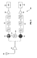
- FIG. 3 illustrates a block circuit diagram of a transceiver according to an embodiment of the present invention.
- FIG. 4 illustrates a circuit diagram of a G m -C bandpass filter.
- FIG. 5 illustrates a circuit diagram of a G m -C bandpass filter according to an embodiment of the present invention.
- FIG. 6A illustrates a circuit diagram of a switchable Gm cell implemented in the circuit of FIG. 5.
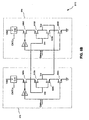
- FIG. 6B illustrates a circuit diagram of two parallel Gm cells implemented in the circuit of FIG. 5.
- FIG. 7 illustrates a circuit diagram of an adjustable resistance G m stage.
- FIG. 8 illustrates a Gain (dB) vs. frequency chart for the filter of FIG. 5 under various operating modes.
- FIG. 3 illustrates a wireless receiver 300, according to an embodiment of the present invention, that includes an antenna 305, a low noise amplifier (LNA) 310, mixers 315 and 320, a local oscillator 325, filter stages 340 and 345, amplifiers 350 and 355, and a pair of analog to digital converters (ADC) 360 and 365.
- LNA low noise amplifier
- ADC analog to digital converter
- RF signals received by antenna 305 are forwarded to LNA 310.
- the received RF signals are single-ended RF signals.
- the received RF signals typically range from 800MHz to 2.1 GHz.
- a GSM network may be implemented at 800MHz or 1.9GHz.
- W-CDMA is typically implemented at 2.1 GHz.
- LNA 310 amplifies RF signals and provide a low noise amplification.
- the amplified signals are then converted into a in-phase (I) signal portion and a quadrature (Q) signal portion by mixers 315 and 320, respectively.
- Mixers 315 and 320 also down converts each of the I and Q signals to a lower frequency signal. Both mixers 315 and 320 operate in the substantial same way, as such only the operation of mixer 315 will be described.
- Mixer 315 mixes the I signal (or Q) with a local signal 327 that is generated by a voltage control oscillator (VCO) 325.
- VCO voltage control oscillator
- the input I signal or (Q signal) is down converted to an intermediate frequency signal by mixer 315.
- the IF signal has a center frequency of 200KHz and a frequency bandwidth of 200KHz.
- the IF signal has a center frequency of 1MHz and a frequency bandwidth of 1.8MHz.
- the IF signal may be amplified by an IF amplifier (not shown). After amplification, the IF signal is feed through filter stage 340.
- Filter stage 340 comprises several stages of filters and variable gain amplifiers. Filter stage 340 also performs DC offset rejection, signal amplification, and bandpass filtration. In this way, the IF signal may be processed to obtain the proper gain and frequency bandwidth.
- filter stage 340 comprises multiple stages of Butterworth filters.
- filter stage 340 comprises multiple stages of Chebyshev or Bessel filters. A combination of Butterworth, Chebyshev or Bessel filters may also be used.
- Filter stage 345 is implemented in the same way as filter stage 340.
- the output of filter stage 340 or 345 may further be amplified using amplifier 350 and 355.
- This amplification stage is optional and generally depends on the application.
- the amplified signal is routed to an analog to digital converter (ADC) 360/365.
- ADC analog to digital converter
- receiver 300 is implemented using a conventional transconductor capacitor (G m C) bandpass (BP) filter 400, such as the one shown in FIG. 4. Filter 400 will be further discussed below.
- receiver 300 is implemented using a reconfigurable G m C bandpass filter 500, such as the one shown in FIG. 5. G m C bandpass filter 500 will be further discussed below.
- G m C bandpass filter 400 includes three G m stages 410, 420, and 430, a resistor 440, a capacitor 450, a second resistor 460, and a second capacitor 470.
- Resistor 440 and capacitor 450 provide a first resistor-capacitor pair that generally determines the bandwidth frequency of filter 400.
- Resistor 460 and capacitor 470 provide a second resistor-capacitor pair that determines the center frequency of filter 400.
- the RC constant of the resistor 440-capacitor 450 pair may be adjusted.
- the RC constant of the resistor 460-capacitor 470 pair may be adjusted.
- G m stage 410 is used to primarily control the overall signal gain of filter 400.
- G m stages 420 and 430 are used to primarily control the overall frequency response of filter 400.
- reconfigurable G m C bandpass filter 500 includes three programmable G m stages 510, 520, and 530, a resistor 540, a capacitor 550, a second resistor 560, and a second capacitor 570.
- capacitors 550 and 570 are adjustable capacitors. These adjustable capacitors serve to compensate for the system processing corners or variations. Adjustable capacitors are well known in the art. Further, resistors 540 and 560 may also be adjustable and may be implemented as a variable G m stage as shown in FIG. 7, which will be further discussed below.
- G m stages 510, 520, and 530 are programmable or reconfigurable in order to increase the overall G m of the system.
- the frequency response of the filter may be manipulated.
- the frequency response of a filter may be affected by changing the time constant of the filter, the RC value.
- Filter 500 is a multi-standard filter because its G m may be adjusted such that the frequency response of filter 500 is dramatically changed.
- the IF center frequency of a GSM system is approximately 200KHz and approximately 1000KHz for a W-CDMA system.
- Filter 500 can operate in either environment by increasing or lowering the G m value of G m stages 510, 520, and 530.
- the G m of the G m stages 510, 520, and 530 has to be increased relative to where the G m value is set at for GSM application.
- G m stage 510 includes G m circuits 512 and 514.
- G m stage 520 includes G m circuits 522 and 524.
- G m stage 530 includes G m circuits 532 and 534.
- Each of the G m circuits 514, 524, and 534 has a larger G m value than its respective parallel G m stage.
- the G m of circuit 514 is 10 times greater than G m of circuit 512.
- the G m of circuits 524 and 534 is 10 times greater than the G m of circuits 522 and 532, respectively.
- the each of the G m of circuits 514, 524, and 534 is 10 times greater than the Gm of the respective parallel circuit, other multiples could also be employed such as 15x, 20x, etc.
- G m circuits 512, 522, and 532 are enabled and G m circuits 514, 524, and 532 are disabled to provide the necessary gain and IF characteristics for GSM operation. In this manner, only one of the G m circuit of the parallel circuit pair (e.g. G m stage 510 or 520) is enabled at any time.
- G m circuits 512, 522, and 532 are disabled and G m circuits 514, 524, and 532 are enabled to provide the necessary gain and IF characteristics for W-CDMA operation. In this manner, filter 500 exhibits a larger overall G m and yields a larger IF frequency (compared to GSM) as required W-CDMA.
- both circuits of the parallel circuit pair could be enabled at the same time.
- the G m ratio of the circuit pair would have to be manipulated such that the parallel G m circuit pair would yield a desired G m value.
- G m stage 510 may be configured such that both G m circuits 512 and 514 are enabled in GSM mode, and 1 of the G m circuits 512 and 514 is disabled in W-CDMA mode.
- the G m of a G m circuits may be controlled with many methods.
- One of the methods is to manipulate the transistor's channel width and length ratio.
- the relationship between G m , channel length, and width is: G m ⁇ ⁇ Width Length
- the surface area of G m circuits 512 and 514 are generally the same.
- the major difference is in the W/L ratio of transistors in each of the circuits.
- the W/L ratio for circuit 512 may be 2 ⁇ /6.3 ⁇ ⁇ 0.317.
- the W/L ratio is reversed, 6.3 ⁇ /2 ⁇ ⁇ 3.150.
- FIG. 6A illustrates a G m cell 600, which is one example embodiment that can be used to implement the G m circuit of G m stages 510, 520, and 530.
- G m cell 600 includes two positive channel metal oxide semiconductors (PMOS) 610 and 620 and two negative channel MOS (NMOS) 630 and 640.
- the gates of PMOS 620 and NMOS 630 are coupled to a voltage input.
- the drains of PMOS 620 and NMOS 630 are coupled together and comprise the output node in which I out is obtained.
- the source of PMOS 610 is coupled to a voltage controller.
- the drain of PMOS 610 is coupled to the source of PMOS 620.
- the source of NMOS 640 is coupled to ground and the drain is coupled to the source of NMOS 630. Both the gates of PMOS 610 and NMOS 640 are coupled together and to a gain controller. Further an inverter is coupled to the gate of PMOS 610.
- FIG. 6B illustrates an example implementation of G m stage 510.
- G m stage 510 includes G m circuits 512 and 514 connected in parallel.
- the input nodes of circuits 512 and 514 are commonly coupled to an input source (not shown).
- the output nodes of circuits 512 and 514 are commonly coupled to an output node.
- Transistors 605A-B, 615A-B, 625A-B, and 635A-B are similar to transistors 610, 620, 630, and 640 of G m cell 600.
- the cell with a smaller G m value is enabled and the cell with the larger G m value is disabled.
- G m stage 510 may be configured such that both cells are enabled for GSM mode and only 1 of the cell is enabled for W-CDMA mode or vice versa. Such configuration may be readily performed by one skilled in the art.
- FIG. 7 illustrates a G m stage 700, which is one example embodiment that can be used to implement adjustable resistors 540 and 560.
- the change in G m affects the bandwidth of G m C filter 500.
- the change in G m affects the center frequency of G m C filter 500.
- G m stage 700 may be regulated to obtain a desired bandwidth and center frequency.
- Gm can be regulated the same way as illustrated in Fig 6A and Fig 6B.
- FIG. 8 illustrates a frequency vs. dB chart for GmC filter 500. As shown, the frequency bandwidth of W-CDMA mode is approximately 10 times the bandwidth of GSM mode.
Landscapes
- Engineering & Computer Science (AREA)
- Power Engineering (AREA)
- Networks Using Active Elements (AREA)
- Transceivers (AREA)
- Superheterodyne Receivers (AREA)
- Circuits Of Receivers In General (AREA)
Applications Claiming Priority (2)
| Application Number | Priority Date | Filing Date | Title |
|---|---|---|---|
| US81337506P | 2006-06-14 | 2006-06-14 | |
| US11/492,983 US7417495B2 (en) | 2006-06-14 | 2006-07-26 | Reconfigurable frequency filter |
Publications (2)
| Publication Number | Publication Date |
|---|---|
| EP1868290A2 true EP1868290A2 (de) | 2007-12-19 |
| EP1868290A3 EP1868290A3 (de) | 2008-03-12 |
Family
ID=38537553
Family Applications (1)
| Application Number | Title | Priority Date | Filing Date |
|---|---|---|---|
| EP07004090A Withdrawn EP1868290A3 (de) | 2006-06-14 | 2007-02-27 | Rekonfigurierbares Frequenzfilter |
Country Status (5)
| Country | Link |
|---|---|
| US (1) | US7417495B2 (de) |
| EP (1) | EP1868290A3 (de) |
| KR (1) | KR100882406B1 (de) |
| CN (1) | CN101106362B (de) |
| TW (1) | TWI366979B (de) |
Families Citing this family (5)
| Publication number | Priority date | Publication date | Assignee | Title |
|---|---|---|---|---|
| US8514829B2 (en) | 2007-10-05 | 2013-08-20 | Qualcomm Incorporated | Center frequency control for wireless communication |
| US8265568B2 (en) * | 2009-03-19 | 2012-09-11 | Qualcomm Incorporated | Frequency divider with synchronized outputs |
| US9602079B2 (en) * | 2009-06-23 | 2017-03-21 | Qualcomm Incorporated | Tunable adaptive filter with variable gain trans-conductance stage |
| WO2012150942A1 (en) * | 2011-05-05 | 2012-11-08 | Nuance Communications, Inc. | Low-delay filtering |
| CN105513984B (zh) * | 2014-09-24 | 2018-06-26 | 北大方正集团有限公司 | Mos管的实际沟道长度的测试方法及装置 |
Citations (2)
| Publication number | Priority date | Publication date | Assignee | Title |
|---|---|---|---|---|
| US5621340A (en) | 1995-08-02 | 1997-04-15 | Rambus Inc. | Differential comparator for amplifying small swing signals to a full swing output |
| US20030006834A1 (en) | 2000-01-31 | 2003-01-09 | Takashi Morie | Transconductor and filter circuit |
Family Cites Families (8)
| Publication number | Priority date | Publication date | Assignee | Title |
|---|---|---|---|---|
| KR100263300B1 (ko) * | 1997-09-12 | 2000-08-01 | 정선종 | 필터의 튜닝 회로 |
| KR100283619B1 (ko) * | 1998-12-03 | 2001-03-02 | 정선종 | 연속-시간 필터를 위한 주파수 튜닝 회로 |
| US6304134B1 (en) * | 2000-03-29 | 2001-10-16 | Texas Instruments Incorporated | High-frequency boost technique |
| JP3584893B2 (ja) * | 2001-03-14 | 2004-11-04 | ソニー株式会社 | フィルタ回路 |
| US6480064B1 (en) * | 2001-05-25 | 2002-11-12 | Infineon Technologies Ag | Method and apparatus for an efficient low voltage switchable Gm cell |
| US6891436B2 (en) * | 2002-09-30 | 2005-05-10 | Integrant Technologies Inc. | Transconductance varying circuit of transconductor circuit, varying bandwidth filter circuit using the same and digital tuning circuit of transconductor-capacitor filter |
| JP3953009B2 (ja) * | 2003-09-12 | 2007-08-01 | ソニー株式会社 | トランスコンダクタンス調整回路 |
| US7236054B2 (en) * | 2004-01-28 | 2007-06-26 | Silicon Storage Technology, Inc. | Multi-operational amplifier system |
-
2006
- 2006-07-26 US US11/492,983 patent/US7417495B2/en not_active Expired - Fee Related
-
2007
- 2007-02-27 EP EP07004090A patent/EP1868290A3/de not_active Withdrawn
- 2007-06-12 CN CN2007101119465A patent/CN101106362B/zh not_active Expired - Fee Related
- 2007-06-13 KR KR1020070057775A patent/KR100882406B1/ko not_active Expired - Fee Related
- 2007-06-13 TW TW096121323A patent/TWI366979B/zh not_active IP Right Cessation
Patent Citations (2)
| Publication number | Priority date | Publication date | Assignee | Title |
|---|---|---|---|---|
| US5621340A (en) | 1995-08-02 | 1997-04-15 | Rambus Inc. | Differential comparator for amplifying small swing signals to a full swing output |
| US20030006834A1 (en) | 2000-01-31 | 2003-01-09 | Takashi Morie | Transconductor and filter circuit |
Also Published As
| Publication number | Publication date |
|---|---|
| TW200820599A (en) | 2008-05-01 |
| TWI366979B (en) | 2012-06-21 |
| CN101106362B (zh) | 2011-11-23 |
| US20070290737A1 (en) | 2007-12-20 |
| KR20070119528A (ko) | 2007-12-20 |
| EP1868290A3 (de) | 2008-03-12 |
| KR100882406B1 (ko) | 2009-02-05 |
| US7417495B2 (en) | 2008-08-26 |
| HK1116935A1 (en) | 2009-01-02 |
| CN101106362A (zh) | 2008-01-16 |
Similar Documents
| Publication | Publication Date | Title |
|---|---|---|
| US8301101B2 (en) | Frequency translated filter | |
| US10205438B2 (en) | Adjustable low-pass filter in a compact low-power receiver | |
| US8805314B2 (en) | Filter circuit and receiving device | |
| US7705682B2 (en) | Inductor sharing in radio frequency communications | |
| EP3142254B1 (de) | Funkfrequenzempfängerfrontend mit verstärkungsregelungsfähigkeit sowie verbesserter impedanzanpassungsregelungsfähigkeit | |
| US6972610B2 (en) | High linearity passive mixer and associated LO buffer | |
| US8224275B2 (en) | Area reduction techniques for saw-less receivers | |
| US8019314B2 (en) | Radio communication apparatus | |
| CN101611556A (zh) | 用于接收射频信号的方法和装置 | |
| US20060276159A1 (en) | Low noise amplifier with constant input impedance | |
| US8238862B2 (en) | Layout techniques for frequency translated filters | |
| GB2415844A (en) | Programmable gain amplifier with reduced gain switching transients | |
| EP1868290A2 (de) | Rekonfigurierbares Frequenzfilter | |
| US6831506B1 (en) | Reconfigurable filter architecture | |
| Yanduru et al. | A WCDMA, GSM/GPRS/EDGE receiver front end without interstage SAW filter | |
| EP1958327B1 (de) | Transkonduktanzstufe mit gemeinsamem gate und gemeinsamer source für einen rf-abwärtswandlungsmischer | |
| EP1679789B1 (de) | Mischerschaltung mit Verstärkungsregelung | |
| KR20020026354A (ko) | 자동이득제어 기능을 가지는 저소음 저왜곡의다중화가능한 길버트 믹서 신호처리 시스템 및 방법 | |
| US20070040609A1 (en) | Low noise amplifier | |
| US7493097B2 (en) | High dynamic range compact mixer output stage for a wireless receiver | |
| EP2685636B1 (de) | Selbsteinstellende Niederfrequenz-Amplitudenschaltung aus in Hochfrequenz erzeugten Quadratursignalen | |
| US7782127B2 (en) | Multi-mode reconstruction filter | |
| US20040116095A1 (en) | High dynamic range radio frequency mixer | |
| HK1116935B (en) | Transconductance circuit module and radio frequency filter | |
| Park et al. | A direct-conversion CMOS RF receiver reconfigurable from 2GHz to 6GHz |
Legal Events
| Date | Code | Title | Description |
|---|---|---|---|
| PUAI | Public reference made under article 153(3) epc to a published international application that has entered the european phase |
Free format text: ORIGINAL CODE: 0009012 |
|
| AK | Designated contracting states |
Kind code of ref document: A2 Designated state(s): AT BE BG CH CY CZ DE DK EE ES FI FR GB GR HU IE IS IT LI LT LU LV MC NL PL PT RO SE SI SK TR |
|
| AX | Request for extension of the european patent |
Extension state: AL BA HR MK YU |
|
| PUAL | Search report despatched |
Free format text: ORIGINAL CODE: 0009013 |
|
| PUAF | Information related to the publication of a search report (a3 document) modified or deleted |
Free format text: ORIGINAL CODE: 0009199SEPU |
|
| AK | Designated contracting states |
Kind code of ref document: A3 Designated state(s): AT BE BG CH CY CZ DE DK EE ES FI FR GB GR HU IE IS IT LI LT LU LV MC NL PL PT RO SE SI SK TR |
|
| AX | Request for extension of the european patent |
Extension state: AL BA HR MK YU |
|
| PUAL | Search report despatched |
Free format text: ORIGINAL CODE: 0009013 |
|
| D17D | Deferred search report published (deleted) | ||
| AK | Designated contracting states |
Kind code of ref document: A3 Designated state(s): AT BE BG CH CY CZ DE DK EE ES FI FR GB GR HU IE IS IT LI LT LU LV MC NL PL PT RO SE SI SK TR |
|
| AX | Request for extension of the european patent |
Extension state: AL BA HR MK YU |
|
| 17P | Request for examination filed |
Effective date: 20080912 |
|
| 17Q | First examination report despatched |
Effective date: 20081013 |
|
| AKX | Designation fees paid |
Designated state(s): DE FR GB |
|
| STAA | Information on the status of an ep patent application or granted ep patent |
Free format text: STATUS: THE APPLICATION IS DEEMED TO BE WITHDRAWN |
|
| 18D | Application deemed to be withdrawn |
Effective date: 20130903 |