EP1868246A1 - Organic el display device, organic transistor and methods for manufacturing such organic el display device and organic transistor - Google Patents
Organic el display device, organic transistor and methods for manufacturing such organic el display device and organic transistor Download PDFInfo
- Publication number
- EP1868246A1 EP1868246A1 EP06729917A EP06729917A EP1868246A1 EP 1868246 A1 EP1868246 A1 EP 1868246A1 EP 06729917 A EP06729917 A EP 06729917A EP 06729917 A EP06729917 A EP 06729917A EP 1868246 A1 EP1868246 A1 EP 1868246A1
- Authority
- EP
- European Patent Office
- Prior art keywords
- organic
- layer
- conductive layer
- display device
- organic transistor
- Prior art date
- Legal status (The legal status is an assumption and is not a legal conclusion. Google has not performed a legal analysis and makes no representation as to the accuracy of the status listed.)
- Withdrawn
Links
- 238000004519 manufacturing process Methods 0.000 title claims abstract description 40
- 238000000034 method Methods 0.000 title description 53
- 238000009413 insulation Methods 0.000 claims abstract description 61
- 239000002245 particle Substances 0.000 claims description 33
- 230000006866 deterioration Effects 0.000 abstract description 3
- 239000010410 layer Substances 0.000 description 176
- 239000010408 film Substances 0.000 description 167
- -1 polypropylene Polymers 0.000 description 66
- 239000000463 material Substances 0.000 description 37
- 230000004888 barrier function Effects 0.000 description 28
- 239000011229 interlayer Substances 0.000 description 28
- 239000000758 substrate Substances 0.000 description 28
- 238000002347 injection Methods 0.000 description 25
- 239000007924 injection Substances 0.000 description 25
- 238000000576 coating method Methods 0.000 description 23
- 239000011248 coating agent Substances 0.000 description 21
- 238000004020 luminiscence type Methods 0.000 description 18
- 239000004065 semiconductor Substances 0.000 description 18
- 239000007787 solid Substances 0.000 description 17
- 229910052751 metal Inorganic materials 0.000 description 16
- 239000002184 metal Substances 0.000 description 16
- 229920000642 polymer Polymers 0.000 description 14
- 230000006870 function Effects 0.000 description 13
- 229920000547 conjugated polymer Polymers 0.000 description 12
- 230000005525 hole transport Effects 0.000 description 11
- 229920005989 resin Polymers 0.000 description 11
- 239000011347 resin Substances 0.000 description 11
- 150000001875 compounds Chemical class 0.000 description 10
- 239000011159 matrix material Substances 0.000 description 10
- QVGXLLKOCUKJST-UHFFFAOYSA-N atomic oxygen Chemical compound [O] QVGXLLKOCUKJST-UHFFFAOYSA-N 0.000 description 9
- 229910044991 metal oxide Inorganic materials 0.000 description 9
- 239000011368 organic material Substances 0.000 description 9
- 239000001301 oxygen Substances 0.000 description 9
- 229910052760 oxygen Inorganic materials 0.000 description 9
- 239000010409 thin film Substances 0.000 description 9
- OKTJSMMVPCPJKN-UHFFFAOYSA-N Carbon Chemical compound [C] OKTJSMMVPCPJKN-UHFFFAOYSA-N 0.000 description 8
- 238000007429 general method Methods 0.000 description 8
- PQXKHYXIUOZZFA-UHFFFAOYSA-M lithium fluoride Chemical compound [Li+].[F-] PQXKHYXIUOZZFA-UHFFFAOYSA-M 0.000 description 8
- 150000004767 nitrides Chemical class 0.000 description 8
- 238000005507 spraying Methods 0.000 description 8
- XLOMVQKBTHCTTD-UHFFFAOYSA-N Zinc monoxide Chemical compound [Zn]=O XLOMVQKBTHCTTD-UHFFFAOYSA-N 0.000 description 7
- 229910052782 aluminium Inorganic materials 0.000 description 7
- 229910052799 carbon Inorganic materials 0.000 description 7
- 230000003628 erosive effect Effects 0.000 description 7
- 150000004706 metal oxides Chemical class 0.000 description 7
- 230000008569 process Effects 0.000 description 7
- 238000004528 spin coating Methods 0.000 description 7
- VYPSYNLAJGMNEJ-UHFFFAOYSA-N Silicium dioxide Chemical compound O=[Si]=O VYPSYNLAJGMNEJ-UHFFFAOYSA-N 0.000 description 6
- 150000002739 metals Chemical class 0.000 description 6
- 229910052814 silicon oxide Inorganic materials 0.000 description 6
- TVIVIEFSHFOWTE-UHFFFAOYSA-K tri(quinolin-8-yloxy)alumane Chemical compound [Al+3].C1=CN=C2C([O-])=CC=CC2=C1.C1=CN=C2C([O-])=CC=CC2=C1.C1=CN=C2C([O-])=CC=CC2=C1 TVIVIEFSHFOWTE-UHFFFAOYSA-K 0.000 description 6
- 239000004952 Polyamide Substances 0.000 description 5
- 239000004642 Polyimide Substances 0.000 description 5
- 239000004372 Polyvinyl alcohol Substances 0.000 description 5
- 238000007733 ion plating Methods 0.000 description 5
- 150000002736 metal compounds Chemical class 0.000 description 5
- 229920002647 polyamide Polymers 0.000 description 5
- 229920000767 polyaniline Polymers 0.000 description 5
- 229920001721 polyimide Polymers 0.000 description 5
- 229920000123 polythiophene Polymers 0.000 description 5
- 229920002451 polyvinyl alcohol Polymers 0.000 description 5
- 229910052709 silver Inorganic materials 0.000 description 5
- 238000003980 solgel method Methods 0.000 description 5
- IJGRMHOSHXDMSA-UHFFFAOYSA-N Atomic nitrogen Chemical compound N#N IJGRMHOSHXDMSA-UHFFFAOYSA-N 0.000 description 4
- 229910005451 FeTiO3 Inorganic materials 0.000 description 4
- 229910005831 GeO3 Inorganic materials 0.000 description 4
- 229910026161 MgAl2O4 Inorganic materials 0.000 description 4
- 229910017676 MgTiO3 Inorganic materials 0.000 description 4
- KAESVJOAVNADME-UHFFFAOYSA-N Pyrrole Chemical compound C=1C=CNC=1 KAESVJOAVNADME-UHFFFAOYSA-N 0.000 description 4
- 229910052581 Si3N4 Inorganic materials 0.000 description 4
- 229910004205 SiNX Inorganic materials 0.000 description 4
- 229910004273 TeO3 Inorganic materials 0.000 description 4
- YTPLMLYBLZKORZ-UHFFFAOYSA-N Thiophene Chemical compound C=1C=CSC=1 YTPLMLYBLZKORZ-UHFFFAOYSA-N 0.000 description 4
- 229910010421 TiNx Inorganic materials 0.000 description 4
- 229910010252 TiO3 Inorganic materials 0.000 description 4
- 229910003087 TiOx Inorganic materials 0.000 description 4
- XAGFODPZIPBFFR-UHFFFAOYSA-N aluminium Chemical compound [Al] XAGFODPZIPBFFR-UHFFFAOYSA-N 0.000 description 4
- 238000005229 chemical vapour deposition Methods 0.000 description 4
- 230000000052 comparative effect Effects 0.000 description 4
- 230000007423 decrease Effects 0.000 description 4
- 239000003822 epoxy resin Substances 0.000 description 4
- 239000011521 glass Substances 0.000 description 4
- 239000010931 gold Substances 0.000 description 4
- 229910010272 inorganic material Inorganic materials 0.000 description 4
- 239000011147 inorganic material Substances 0.000 description 4
- PXHVJJICTQNCMI-UHFFFAOYSA-N nickel Substances [Ni] PXHVJJICTQNCMI-UHFFFAOYSA-N 0.000 description 4
- 239000012044 organic layer Substances 0.000 description 4
- 229920000647 polyepoxide Polymers 0.000 description 4
- 229920000728 polyester Polymers 0.000 description 4
- 239000000843 powder Substances 0.000 description 4
- LIVNPJMFVYWSIS-UHFFFAOYSA-N silicon monoxide Chemical compound [Si-]#[O+] LIVNPJMFVYWSIS-UHFFFAOYSA-N 0.000 description 4
- 229910052596 spinel Inorganic materials 0.000 description 4
- PBCFLUZVCVVTBY-UHFFFAOYSA-N tantalum pentoxide Inorganic materials O=[Ta](=O)O[Ta](=O)=O PBCFLUZVCVVTBY-UHFFFAOYSA-N 0.000 description 4
- HLLICFJUWSZHRJ-UHFFFAOYSA-N tioxidazole Chemical compound CCCOC1=CC=C2N=C(NC(=O)OC)SC2=C1 HLLICFJUWSZHRJ-UHFFFAOYSA-N 0.000 description 4
- 229920000178 Acrylic resin Polymers 0.000 description 3
- 239000004925 Acrylic resin Substances 0.000 description 3
- YCKRFDGAMUMZLT-UHFFFAOYSA-N Fluorine atom Chemical compound [F] YCKRFDGAMUMZLT-UHFFFAOYSA-N 0.000 description 3
- FUJCRWPEOMXPAD-UHFFFAOYSA-N Li2O Inorganic materials [Li+].[Li+].[O-2] FUJCRWPEOMXPAD-UHFFFAOYSA-N 0.000 description 3
- YNPNZTXNASCQKK-UHFFFAOYSA-N Phenanthrene Natural products C1=CC=C2C3=CC=CC=C3C=CC2=C1 YNPNZTXNASCQKK-UHFFFAOYSA-N 0.000 description 3
- 125000003118 aryl group Chemical group 0.000 description 3
- 239000004020 conductor Substances 0.000 description 3
- 239000002019 doping agent Substances 0.000 description 3
- 229910052731 fluorine Inorganic materials 0.000 description 3
- 239000011737 fluorine Substances 0.000 description 3
- 239000007789 gas Substances 0.000 description 3
- 150000002343 gold Chemical class 0.000 description 3
- RAXXELZNTBOGNW-UHFFFAOYSA-N imidazole Chemical class C1=CNC=N1 RAXXELZNTBOGNW-UHFFFAOYSA-N 0.000 description 3
- 229910052759 nickel Inorganic materials 0.000 description 3
- 229910052758 niobium Inorganic materials 0.000 description 3
- 150000002894 organic compounds Chemical class 0.000 description 3
- SLIUAWYAILUBJU-UHFFFAOYSA-N pentacene Chemical compound C1=CC=CC2=CC3=CC4=CC5=CC=CC=C5C=C4C=C3C=C21 SLIUAWYAILUBJU-UHFFFAOYSA-N 0.000 description 3
- 125000002080 perylenyl group Chemical group C1(=CC=C2C=CC=C3C4=CC=CC5=CC=CC(C1=C23)=C45)* 0.000 description 3
- CSHWQDPOILHKBI-UHFFFAOYSA-N peryrene Natural products C1=CC(C2=CC=CC=3C2=C2C=CC=3)=C3C2=CC=CC3=C1 CSHWQDPOILHKBI-UHFFFAOYSA-N 0.000 description 3
- 229920000553 poly(phenylenevinylene) Polymers 0.000 description 3
- 238000007789 sealing Methods 0.000 description 3
- 239000002356 single layer Substances 0.000 description 3
- 239000000126 substance Substances 0.000 description 3
- 229910052719 titanium Inorganic materials 0.000 description 3
- 238000001771 vacuum deposition Methods 0.000 description 3
- 238000007738 vacuum evaporation Methods 0.000 description 3
- 229910052725 zinc Inorganic materials 0.000 description 3
- 239000011701 zinc Substances 0.000 description 3
- 239000011787 zinc oxide Substances 0.000 description 3
- 229910052726 zirconium Inorganic materials 0.000 description 3
- NNDLQUNWZOIESH-UHFFFAOYSA-N 8-hydroxy-7-[[7-[(8-hydroxy-5-sulfoquinoline-7-carbonyl)amino]-4-[3-[(8-hydroxy-5-sulfoquinoline-7-carbonyl)amino]propyl]heptyl]carbamoyl]quinoline-5-sulfonic acid Chemical compound C1=CC=NC2=C(O)C(C(=O)NCCCC(CCCNC(=O)C=3C(=C4N=CC=CC4=C(C=3)S(O)(=O)=O)O)CCCNC(=O)C3=C(C4=NC=CC=C4C(=C3)S(O)(=O)=O)O)=CC(S(O)(=O)=O)=C21 NNDLQUNWZOIESH-UHFFFAOYSA-N 0.000 description 2
- UJOBWOGCFQCDNV-UHFFFAOYSA-N 9H-carbazole Chemical class C1=CC=C2C3=CC=CC=C3NC2=C1 UJOBWOGCFQCDNV-UHFFFAOYSA-N 0.000 description 2
- 229910017988 AgVO3 Inorganic materials 0.000 description 2
- 229910000505 Al2TiO5 Inorganic materials 0.000 description 2
- 229910017107 AlOx Inorganic materials 0.000 description 2
- XKRFYHLGVUSROY-UHFFFAOYSA-N Argon Chemical compound [Ar] XKRFYHLGVUSROY-UHFFFAOYSA-N 0.000 description 2
- 229910017257 AsOx Inorganic materials 0.000 description 2
- 229910016010 BaAl2 Inorganic materials 0.000 description 2
- 229910002771 BaFe12O19 Inorganic materials 0.000 description 2
- 229910015805 BaWO4 Inorganic materials 0.000 description 2
- XMWRBQBLMFGWIX-UHFFFAOYSA-N C60 fullerene Chemical class C12=C3C(C4=C56)=C7C8=C5C5=C9C%10=C6C6=C4C1=C1C4=C6C6=C%10C%10=C9C9=C%11C5=C8C5=C8C7=C3C3=C7C2=C1C1=C2C4=C6C4=C%10C6=C9C9=C%11C5=C5C8=C3C3=C7C1=C1C2=C4C6=C2C9=C5C3=C12 XMWRBQBLMFGWIX-UHFFFAOYSA-N 0.000 description 2
- 229910002971 CaTiO3 Inorganic materials 0.000 description 2
- 229910004829 CaWO4 Inorganic materials 0.000 description 2
- 229910002976 CaZrO3 Inorganic materials 0.000 description 2
- 101150051353 Canx gene Proteins 0.000 description 2
- 229910004605 CdOx Inorganic materials 0.000 description 2
- 229910004607 CdSnO3 Inorganic materials 0.000 description 2
- 229910002979 CdTiO3 Inorganic materials 0.000 description 2
- 229910003320 CeOx Inorganic materials 0.000 description 2
- 229910052684 Cerium Inorganic materials 0.000 description 2
- 229910021556 Chromium(III) chloride Inorganic materials 0.000 description 2
- 229910002518 CoFe2O4 Inorganic materials 0.000 description 2
- 229910018864 CoMoO4 Inorganic materials 0.000 description 2
- 229910002451 CoOx Inorganic materials 0.000 description 2
- 229910021589 Copper(I) bromide Inorganic materials 0.000 description 2
- 229910019923 CrOx Inorganic materials 0.000 description 2
- VMQMZMRVKUZKQL-UHFFFAOYSA-N Cu+ Chemical compound [Cu+] VMQMZMRVKUZKQL-UHFFFAOYSA-N 0.000 description 2
- 229910002477 CuCr2O4 Inorganic materials 0.000 description 2
- 229910016547 CuNx Inorganic materials 0.000 description 2
- 229910016553 CuOx Inorganic materials 0.000 description 2
- 229910052692 Dysprosium Inorganic materials 0.000 description 2
- 229910052691 Erbium Inorganic materials 0.000 description 2
- 239000005977 Ethylene Substances 0.000 description 2
- 229910002539 EuFeO3 Inorganic materials 0.000 description 2
- 229910052693 Europium Inorganic materials 0.000 description 2
- 229910015183 FeNx Inorganic materials 0.000 description 2
- 229910015189 FeOx Inorganic materials 0.000 description 2
- 229910005507 FeWO4 Inorganic materials 0.000 description 2
- YLQBMQCUIZJEEH-UHFFFAOYSA-N Furan Chemical compound C=1C=COC=1 YLQBMQCUIZJEEH-UHFFFAOYSA-N 0.000 description 2
- 229910005535 GaOx Inorganic materials 0.000 description 2
- 229910052688 Gadolinium Inorganic materials 0.000 description 2
- 229910002608 Gd3Fe5O12 Inorganic materials 0.000 description 2
- 229910002618 GdFeO3 Inorganic materials 0.000 description 2
- 229910002616 GeOx Inorganic materials 0.000 description 2
- 229910052689 Holmium Inorganic materials 0.000 description 2
- SIKJAQJRHWYJAI-UHFFFAOYSA-N Indole Chemical class C1=CC=C2NC=CC2=C1 SIKJAQJRHWYJAI-UHFFFAOYSA-N 0.000 description 2
- 229910021577 Iron(II) chloride Inorganic materials 0.000 description 2
- 229910021579 Iron(II) iodide Inorganic materials 0.000 description 2
- 229910020435 K2MoO4 Inorganic materials 0.000 description 2
- 229910020451 K2SiO3 Inorganic materials 0.000 description 2
- 229910020494 K2WO4 Inorganic materials 0.000 description 2
- 229910017582 La2Ti2O7 Inorganic materials 0.000 description 2
- 229910002321 LaFeO3 Inorganic materials 0.000 description 2
- 241000079947 Lanx Species 0.000 description 2
- 229910009740 Li2GeO3 Inorganic materials 0.000 description 2
- 229910007562 Li2SiO3 Inorganic materials 0.000 description 2
- 229910007848 Li2TiO3 Inorganic materials 0.000 description 2
- 229910010092 LiAlO2 Inorganic materials 0.000 description 2
- 229910012985 LiVO3 Inorganic materials 0.000 description 2
- 229910052765 Lutetium Inorganic materials 0.000 description 2
- 229910021568 Manganese(II) bromide Inorganic materials 0.000 description 2
- 229910017902 MgIn2O4 Inorganic materials 0.000 description 2
- 229910017947 MgOx Inorganic materials 0.000 description 2
- 229910017163 MnFe2O4 Inorganic materials 0.000 description 2
- 229910016978 MnOx Inorganic materials 0.000 description 2
- 229910015617 MoNx Inorganic materials 0.000 description 2
- 229910015667 MoO4 Inorganic materials 0.000 description 2
- 229910015711 MoOx Inorganic materials 0.000 description 2
- 101100126329 Mus musculus Islr2 gene Proteins 0.000 description 2
- 101100096038 Mus musculus Smox gene Proteins 0.000 description 2
- 229910003206 NH4VO3 Inorganic materials 0.000 description 2
- 229910004619 Na2MoO4 Inorganic materials 0.000 description 2
- 229910003424 Na2SeO3 Inorganic materials 0.000 description 2
- 229910020350 Na2WO4 Inorganic materials 0.000 description 2
- 229910021311 NaFeO2 Inorganic materials 0.000 description 2
- 229910003378 NaNbO3 Inorganic materials 0.000 description 2
- 229910003256 NaTaO3 Inorganic materials 0.000 description 2
- 229910052779 Neodymium Inorganic materials 0.000 description 2
- 229910005809 NiMoO4 Inorganic materials 0.000 description 2
- 229910005855 NiOx Inorganic materials 0.000 description 2
- 229910020662 PbSiO3 Inorganic materials 0.000 description 2
- 229910003781 PbTiO3 Inorganic materials 0.000 description 2
- 229910002673 PdOx Inorganic materials 0.000 description 2
- 229920001774 Perfluoroether Polymers 0.000 description 2
- 239000004698 Polyethylene Substances 0.000 description 2
- 229920000265 Polyparaphenylene Polymers 0.000 description 2
- 229910002830 PrOx Inorganic materials 0.000 description 2
- 229910052777 Praseodymium Inorganic materials 0.000 description 2
- 229910002842 PtOx Inorganic materials 0.000 description 2
- 229910019897 RuOx Inorganic materials 0.000 description 2
- 229910052772 Samarium Inorganic materials 0.000 description 2
- 229910018316 SbOx Inorganic materials 0.000 description 2
- 229910003564 SiAlON Inorganic materials 0.000 description 2
- BLRPTPMANUNPDV-UHFFFAOYSA-N Silane Chemical compound [SiH4] BLRPTPMANUNPDV-UHFFFAOYSA-N 0.000 description 2
- XUIMIQQOPSSXEZ-UHFFFAOYSA-N Silicon Chemical compound [Si] XUIMIQQOPSSXEZ-UHFFFAOYSA-N 0.000 description 2
- 229910021175 SmF3 Inorganic materials 0.000 description 2
- 229910006694 SnO2—Sb2O3 Inorganic materials 0.000 description 2
- 229910006854 SnOx Inorganic materials 0.000 description 2
- 229910003669 SrAl2O4 Inorganic materials 0.000 description 2
- 229910002402 SrFe12O19 Inorganic materials 0.000 description 2
- 229910002347 SrOx Inorganic materials 0.000 description 2
- 229910004410 SrSnO3 Inorganic materials 0.000 description 2
- 229910002370 SrTiO3 Inorganic materials 0.000 description 2
- 229910004415 SrWO4 Inorganic materials 0.000 description 2
- 239000005084 Strontium aluminate Substances 0.000 description 2
- 229910004156 TaNx Inorganic materials 0.000 description 2
- 229910003070 TaOx Inorganic materials 0.000 description 2
- 229910052771 Terbium Inorganic materials 0.000 description 2
- FZWLAAWBMGSTSO-UHFFFAOYSA-N Thiazole Chemical class C1=CSC=N1 FZWLAAWBMGSTSO-UHFFFAOYSA-N 0.000 description 2
- 229910052775 Thulium Inorganic materials 0.000 description 2
- 229910009493 Y3Fe5O12 Inorganic materials 0.000 description 2
- 229910052769 Ytterbium Inorganic materials 0.000 description 2
- 229910001308 Zinc ferrite Inorganic materials 0.000 description 2
- 229910007667 ZnOx Inorganic materials 0.000 description 2
- 229910008328 ZrNx Inorganic materials 0.000 description 2
- 229910003134 ZrOx Inorganic materials 0.000 description 2
- SMEGJBVQLJJKKX-HOTMZDKISA-N [(2R,3S,4S,5R,6R)-5-acetyloxy-3,4,6-trihydroxyoxan-2-yl]methyl acetate Chemical compound CC(=O)OC[C@@H]1[C@H]([C@@H]([C@H]([C@@H](O1)O)OC(=O)C)O)O SMEGJBVQLJJKKX-HOTMZDKISA-N 0.000 description 2
- 239000006096 absorbing agent Substances 0.000 description 2
- 238000010521 absorption reaction Methods 0.000 description 2
- 229940081735 acetylcellulose Drugs 0.000 description 2
- 150000004703 alkoxides Chemical class 0.000 description 2
- 229910045601 alloy Inorganic materials 0.000 description 2
- 239000000956 alloy Substances 0.000 description 2
- HSFWRNGVRCDJHI-UHFFFAOYSA-N alpha-acetylene Natural products C#C HSFWRNGVRCDJHI-UHFFFAOYSA-N 0.000 description 2
- PNEYBMLMFCGWSK-UHFFFAOYSA-N aluminium oxide Inorganic materials [O-2].[O-2].[O-2].[Al+3].[Al+3] PNEYBMLMFCGWSK-UHFFFAOYSA-N 0.000 description 2
- 229910003481 amorphous carbon Inorganic materials 0.000 description 2
- MWPLVEDNUUSJAV-UHFFFAOYSA-N anthracene Chemical compound C1=CC=CC2=CC3=CC=CC=C3C=C21 MWPLVEDNUUSJAV-UHFFFAOYSA-N 0.000 description 2
- 229910002113 barium titanate Inorganic materials 0.000 description 2
- 229910021523 barium zirconate Inorganic materials 0.000 description 2
- 239000002585 base Substances 0.000 description 2
- 239000011230 binding agent Substances 0.000 description 2
- 230000000903 blocking effect Effects 0.000 description 2
- 229910052793 cadmium Inorganic materials 0.000 description 2
- 229920002301 cellulose acetate Polymers 0.000 description 2
- 239000003795 chemical substances by application Substances 0.000 description 2
- RCTYPNKXASFOBE-UHFFFAOYSA-M chloromercury Chemical compound [Hg]Cl RCTYPNKXASFOBE-UHFFFAOYSA-M 0.000 description 2
- QSWDMMVNRMROPK-UHFFFAOYSA-K chromium(3+) trichloride Chemical compound [Cl-].[Cl-].[Cl-].[Cr+3] QSWDMMVNRMROPK-UHFFFAOYSA-K 0.000 description 2
- 239000011636 chromium(III) chloride Substances 0.000 description 2
- 229910052681 coesite Inorganic materials 0.000 description 2
- 239000003086 colorant Substances 0.000 description 2
- 150000004696 coordination complex Chemical class 0.000 description 2
- VPUGDVKSAQVFFS-UHFFFAOYSA-N coronene Chemical compound C1=C(C2=C34)C=CC3=CC=C(C=C3)C4=C4C3=CC=C(C=C3)C4=C2C3=C1 VPUGDVKSAQVFFS-UHFFFAOYSA-N 0.000 description 2
- 229910052593 corundum Inorganic materials 0.000 description 2
- 230000008878 coupling Effects 0.000 description 2
- 238000010168 coupling process Methods 0.000 description 2
- 238000005859 coupling reaction Methods 0.000 description 2
- 229910052906 cristobalite Inorganic materials 0.000 description 2
- 239000010432 diamond Substances 0.000 description 2
- 229910003460 diamond Inorganic materials 0.000 description 2
- RJYMRRJVDRJMJW-UHFFFAOYSA-L dibromomanganese Chemical compound Br[Mn]Br RJYMRRJVDRJMJW-UHFFFAOYSA-L 0.000 description 2
- XUCJHNOBJLKZNU-UHFFFAOYSA-M dilithium;hydroxide Chemical compound [Li+].[Li+].[OH-] XUCJHNOBJLKZNU-UHFFFAOYSA-M 0.000 description 2
- 229910001676 gahnite Inorganic materials 0.000 description 2
- PVADDRMAFCOOPC-UHFFFAOYSA-N germanium monoxide Inorganic materials [Ge]=O PVADDRMAFCOOPC-UHFFFAOYSA-N 0.000 description 2
- PCHJSUWPFVWCPO-UHFFFAOYSA-N gold Chemical compound [Au] PCHJSUWPFVWCPO-UHFFFAOYSA-N 0.000 description 2
- 229910052737 gold Inorganic materials 0.000 description 2
- 238000007756 gravure coating Methods 0.000 description 2
- NNGHIEIYUJKFQS-UHFFFAOYSA-L hydroxy(oxo)iron;zinc Chemical compound [Zn].O[Fe]=O.O[Fe]=O NNGHIEIYUJKFQS-UHFFFAOYSA-L 0.000 description 2
- 229910052909 inorganic silicate Inorganic materials 0.000 description 2
- 229910052741 iridium Inorganic materials 0.000 description 2
- 229910052742 iron Inorganic materials 0.000 description 2
- NMCUIPGRVMDVDB-UHFFFAOYSA-L iron dichloride Chemical compound Cl[Fe]Cl NMCUIPGRVMDVDB-UHFFFAOYSA-L 0.000 description 2
- VRIVJOXICYMTAG-IYEMJOQQSA-L iron(ii) gluconate Chemical compound [Fe+2].OC[C@@H](O)[C@@H](O)[C@H](O)[C@@H](O)C([O-])=O.OC[C@@H](O)[C@@H](O)[C@H](O)[C@@H](O)C([O-])=O VRIVJOXICYMTAG-IYEMJOQQSA-L 0.000 description 2
- BQZGVMWPHXIKEQ-UHFFFAOYSA-L iron(ii) iodide Chemical compound [Fe+2].[I-].[I-] BQZGVMWPHXIKEQ-UHFFFAOYSA-L 0.000 description 2
- 230000001678 irradiating effect Effects 0.000 description 2
- 238000003475 lamination Methods 0.000 description 2
- 229910052746 lanthanum Inorganic materials 0.000 description 2
- 229910052745 lead Inorganic materials 0.000 description 2
- RQQRAHKHDFPBMC-UHFFFAOYSA-L lead(ii) iodide Chemical compound I[Pb]I RQQRAHKHDFPBMC-UHFFFAOYSA-L 0.000 description 2
- 239000002932 luster Substances 0.000 description 2
- 229910052749 magnesium Inorganic materials 0.000 description 2
- 229910001635 magnesium fluoride Inorganic materials 0.000 description 2
- 229910052748 manganese Inorganic materials 0.000 description 2
- 229910001512 metal fluoride Inorganic materials 0.000 description 2
- 229910052757 nitrogen Inorganic materials 0.000 description 2
- FULFYAFFAGNFJM-UHFFFAOYSA-N oxocopper;oxo(oxochromiooxy)chromium Chemical compound [Cu]=O.O=[Cr]O[Cr]=O FULFYAFFAGNFJM-UHFFFAOYSA-N 0.000 description 2
- UJMWVICAENGCRF-UHFFFAOYSA-N oxygen difluoride Chemical compound FOF UJMWVICAENGCRF-UHFFFAOYSA-N 0.000 description 2
- 229910052763 palladium Inorganic materials 0.000 description 2
- 239000005011 phenolic resin Substances 0.000 description 2
- 239000000049 pigment Substances 0.000 description 2
- 229910052697 platinum Inorganic materials 0.000 description 2
- 229920001197 polyacetylene Polymers 0.000 description 2
- 229920000058 polyacrylate Polymers 0.000 description 2
- 229920000515 polycarbonate Polymers 0.000 description 2
- 239000004417 polycarbonate Substances 0.000 description 2
- 229920000573 polyethylene Polymers 0.000 description 2
- 239000002243 precursor Substances 0.000 description 2
- 238000007639 printing Methods 0.000 description 2
- 230000001737 promoting effect Effects 0.000 description 2
- BBEAQIROQSPTKN-UHFFFAOYSA-N pyrene Chemical compound C1=CC=C2C=CC3=CC=CC4=CC=C1C2=C43 BBEAQIROQSPTKN-UHFFFAOYSA-N 0.000 description 2
- 229910052702 rhenium Inorganic materials 0.000 description 2
- 229910052703 rhodium Inorganic materials 0.000 description 2
- 229910052707 ruthenium Inorganic materials 0.000 description 2
- 229910052706 scandium Inorganic materials 0.000 description 2
- 229910000077 silane Inorganic materials 0.000 description 2
- 239000010703 silicon Substances 0.000 description 2
- 229910052710 silicon Inorganic materials 0.000 description 2
- 239000000377 silicon dioxide Substances 0.000 description 2
- HQVNEWCFYHHQES-UHFFFAOYSA-N silicon nitride Chemical compound N12[Si]34N5[Si]62N3[Si]51N64 HQVNEWCFYHHQES-UHFFFAOYSA-N 0.000 description 2
- 239000004332 silver Substances 0.000 description 2
- ADZWSOLPGZMUMY-UHFFFAOYSA-M silver bromide Chemical compound [Ag]Br ADZWSOLPGZMUMY-UHFFFAOYSA-M 0.000 description 2
- 229910001388 sodium aluminate Inorganic materials 0.000 description 2
- 239000011684 sodium molybdate Substances 0.000 description 2
- TVXXNOYZHKPKGW-UHFFFAOYSA-N sodium molybdate (anhydrous) Chemical compound [Na+].[Na+].[O-][Mo]([O-])(=O)=O TVXXNOYZHKPKGW-UHFFFAOYSA-N 0.000 description 2
- 239000011781 sodium selenite Substances 0.000 description 2
- 229910052911 sodium silicate Inorganic materials 0.000 description 2
- XMVONEAAOPAGAO-UHFFFAOYSA-N sodium tungstate Chemical compound [Na+].[Na+].[O-][W]([O-])(=O)=O XMVONEAAOPAGAO-UHFFFAOYSA-N 0.000 description 2
- MUPJWXCPTRQOKY-UHFFFAOYSA-N sodium;niobium(5+);oxygen(2-) Chemical compound [O-2].[O-2].[O-2].[Na+].[Nb+5] MUPJWXCPTRQOKY-UHFFFAOYSA-N 0.000 description 2
- 239000002904 solvent Substances 0.000 description 2
- 229910052682 stishovite Inorganic materials 0.000 description 2
- 229910014031 strontium zirconium oxide Inorganic materials 0.000 description 2
- 229910052715 tantalum Inorganic materials 0.000 description 2
- BFKJFAAPBSQJPD-UHFFFAOYSA-N tetrafluoroethene Chemical group FC(F)=C(F)F BFKJFAAPBSQJPD-UHFFFAOYSA-N 0.000 description 2
- 229930192474 thiophene Natural products 0.000 description 2
- 229910052718 tin Inorganic materials 0.000 description 2
- 229910052905 tridymite Inorganic materials 0.000 description 2
- ODHXBMXNKOYIBV-UHFFFAOYSA-N triphenylamine Chemical compound C1=CC=CC=C1N(C=1C=CC=CC=1)C1=CC=CC=C1 ODHXBMXNKOYIBV-UHFFFAOYSA-N 0.000 description 2
- 229910052720 vanadium Inorganic materials 0.000 description 2
- 229910052882 wollastonite Inorganic materials 0.000 description 2
- 229910001845 yogo sapphire Inorganic materials 0.000 description 2
- 229910052845 zircon Inorganic materials 0.000 description 2
- QGKMIGUHVLGJBR-UHFFFAOYSA-M (4z)-1-(3-methylbutyl)-4-[[1-(3-methylbutyl)quinolin-1-ium-4-yl]methylidene]quinoline;iodide Chemical class [I-].C12=CC=CC=C2N(CCC(C)C)C=CC1=CC1=CC=[N+](CCC(C)C)C2=CC=CC=C12 QGKMIGUHVLGJBR-UHFFFAOYSA-M 0.000 description 1
- SJHPCNCNNSSLPL-UHFFFAOYSA-N 4-(ethoxymethylene)-2-phenyloxazol-5-one Chemical compound O1C(=O)C(=COCC)N=C1C1=CC=CC=C1 SJHPCNCNNSSLPL-UHFFFAOYSA-N 0.000 description 1
- 229910001316 Ag alloy Inorganic materials 0.000 description 1
- CPELXLSAUQHCOX-UHFFFAOYSA-M Bromide Chemical compound [Br-] CPELXLSAUQHCOX-UHFFFAOYSA-M 0.000 description 1
- JSJDSBQUUOVSQH-UHFFFAOYSA-N CCCC[Ag] Chemical compound CCCC[Ag] JSJDSBQUUOVSQH-UHFFFAOYSA-N 0.000 description 1
- 229920000049 Carbon (fiber) Polymers 0.000 description 1
- 229920000298 Cellophane Polymers 0.000 description 1
- 229920008347 Cellulose acetate propionate Polymers 0.000 description 1
- VEXZGXHMUGYJMC-UHFFFAOYSA-M Chloride anion Chemical compound [Cl-] VEXZGXHMUGYJMC-UHFFFAOYSA-M 0.000 description 1
- 235000001258 Cinchona calisaya Nutrition 0.000 description 1
- ZOSNTSSUDLIQGJ-UHFFFAOYSA-L Cl[Au](Cl)C1=CC=CC=C1 Chemical compound Cl[Au](Cl)C1=CC=CC=C1 ZOSNTSSUDLIQGJ-UHFFFAOYSA-L 0.000 description 1
- RYGMFSIKBFXOCR-UHFFFAOYSA-N Copper Chemical compound [Cu] RYGMFSIKBFXOCR-UHFFFAOYSA-N 0.000 description 1
- 229910021595 Copper(I) iodide Inorganic materials 0.000 description 1
- VGGSQFUCUMXWEO-UHFFFAOYSA-N Ethene Chemical compound C=C VGGSQFUCUMXWEO-UHFFFAOYSA-N 0.000 description 1
- KRHYYFGTRYWZRS-UHFFFAOYSA-M Fluoride anion Chemical compound [F-] KRHYYFGTRYWZRS-UHFFFAOYSA-M 0.000 description 1
- 235000000177 Indigofera tinctoria Nutrition 0.000 description 1
- 229910000733 Li alloy Inorganic materials 0.000 description 1
- 229910013439 LiZr Inorganic materials 0.000 description 1
- 241001025261 Neoraja caerulea Species 0.000 description 1
- 239000000020 Nitrocellulose Substances 0.000 description 1
- ZCQWOFVYLHDMMC-UHFFFAOYSA-N Oxazole Chemical class C1=COC=N1 ZCQWOFVYLHDMMC-UHFFFAOYSA-N 0.000 description 1
- 229910019268 POx Inorganic materials 0.000 description 1
- 229910020669 PbOx Inorganic materials 0.000 description 1
- 229920001609 Poly(3,4-ethylenedioxythiophene) Polymers 0.000 description 1
- 239000004695 Polyether sulfone Substances 0.000 description 1
- 239000004721 Polyphenylene oxide Substances 0.000 description 1
- 239000004734 Polyphenylene sulfide Substances 0.000 description 1
- 239000004743 Polypropylene Substances 0.000 description 1
- 239000004793 Polystyrene Substances 0.000 description 1
- 229920001756 Polyvinyl chloride acetate Polymers 0.000 description 1
- 229920001328 Polyvinylidene chloride Polymers 0.000 description 1
- WTKZEGDFNFYCGP-UHFFFAOYSA-N Pyrazole Chemical class C=1C=NNC=1 WTKZEGDFNFYCGP-UHFFFAOYSA-N 0.000 description 1
- NRCMAYZCPIVABH-UHFFFAOYSA-N Quinacridone Chemical compound N1C2=CC=CC=C2C(=O)C2=C1C=C1C(=O)C3=CC=CC=C3NC1=C2 NRCMAYZCPIVABH-UHFFFAOYSA-N 0.000 description 1
- LOUPRKONTZGTKE-WZBLMQSHSA-N Quinine Natural products C([C@H]([C@H](C1)C=C)C2)C[N@@]1[C@@H]2[C@H](O)C1=CC=NC2=CC=C(OC)C=C21 LOUPRKONTZGTKE-WZBLMQSHSA-N 0.000 description 1
- BQCADISMDOOEFD-UHFFFAOYSA-N Silver Chemical compound [Ag] BQCADISMDOOEFD-UHFFFAOYSA-N 0.000 description 1
- PJANXHGTPQOBST-VAWYXSNFSA-N Stilbene Natural products C=1C=CC=CC=1/C=C/C1=CC=CC=C1 PJANXHGTPQOBST-VAWYXSNFSA-N 0.000 description 1
- UCKMPCXJQFINFW-UHFFFAOYSA-N Sulphide Chemical compound [S-2] UCKMPCXJQFINFW-UHFFFAOYSA-N 0.000 description 1
- GWEVSGVZZGPLCZ-UHFFFAOYSA-N Titan oxide Chemical compound O=[Ti]=O GWEVSGVZZGPLCZ-UHFFFAOYSA-N 0.000 description 1
- 239000007983 Tris buffer Substances 0.000 description 1
- HCHKCACWOHOZIP-UHFFFAOYSA-N Zinc Chemical compound [Zn] HCHKCACWOHOZIP-UHFFFAOYSA-N 0.000 description 1
- DGEZNRSVGBDHLK-UHFFFAOYSA-N [1,10]phenanthroline Chemical compound C1=CN=C2C3=NC=CC=C3C=CC2=C1 DGEZNRSVGBDHLK-UHFFFAOYSA-N 0.000 description 1
- XBXHTOUGJGDVMT-UHFFFAOYSA-N [Ag]c1ccccc1 Chemical compound [Ag]c1ccccc1 XBXHTOUGJGDVMT-UHFFFAOYSA-N 0.000 description 1
- XGQBAQHNKOWRLL-UHFFFAOYSA-N [Eu].C(C1=CC=CC=C1)(=O)C(C(C1=CC=CC=C1)=O)C1=C(C(=NC2=C3N=CC=CC3=CC=C12)C(C(C1=CC=CC=C1)=O)C(C1=CC=CC=C1)=O)C(C(C1=CC=CC=C1)=O)C(C1=CC=CC=C1)=O Chemical compound [Eu].C(C1=CC=CC=C1)(=O)C(C(C1=CC=CC=C1)=O)C1=C(C(=NC2=C3N=CC=CC3=CC=C12)C(C(C1=CC=CC=C1)=O)C(C1=CC=CC=C1)=O)C(C(C1=CC=CC=C1)=O)C(C1=CC=CC=C1)=O XGQBAQHNKOWRLL-UHFFFAOYSA-N 0.000 description 1
- 229920006243 acrylic copolymer Polymers 0.000 description 1
- 239000000654 additive Substances 0.000 description 1
- 238000007754 air knife coating Methods 0.000 description 1
- 125000001931 aliphatic group Chemical group 0.000 description 1
- 239000003513 alkali Substances 0.000 description 1
- 230000005260 alpha ray Effects 0.000 description 1
- PYKYMHQGRFAEBM-UHFFFAOYSA-N anthraquinone Natural products CCC(=O)c1c(O)c2C(=O)C3C(C=CC=C3O)C(=O)c2cc1CC(=O)OC PYKYMHQGRFAEBM-UHFFFAOYSA-N 0.000 description 1
- 150000004056 anthraquinones Chemical class 0.000 description 1
- 239000002518 antifoaming agent Substances 0.000 description 1
- 229910052787 antimony Inorganic materials 0.000 description 1
- WATWJIUSRGPENY-UHFFFAOYSA-N antimony atom Chemical compound [Sb] WATWJIUSRGPENY-UHFFFAOYSA-N 0.000 description 1
- 229910052786 argon Inorganic materials 0.000 description 1
- 239000012298 atmosphere Substances 0.000 description 1
- 229910052790 beryllium Inorganic materials 0.000 description 1
- ATBAMAFKBVZNFJ-UHFFFAOYSA-N beryllium atom Chemical compound [Be] ATBAMAFKBVZNFJ-UHFFFAOYSA-N 0.000 description 1
- 230000005250 beta ray Effects 0.000 description 1
- 238000004061 bleaching Methods 0.000 description 1
- 150000001649 bromium compounds Chemical class 0.000 description 1
- CQEYYJKEWSMYFG-UHFFFAOYSA-N butyl acrylate Chemical compound CCCCOC(=O)C=C CQEYYJKEWSMYFG-UHFFFAOYSA-N 0.000 description 1
- 239000006229 carbon black Substances 0.000 description 1
- 239000004917 carbon fiber Substances 0.000 description 1
- 239000002041 carbon nanotube Substances 0.000 description 1
- 229910021393 carbon nanotube Inorganic materials 0.000 description 1
- 229920002678 cellulose Polymers 0.000 description 1
- 239000001913 cellulose Substances 0.000 description 1
- 150000001805 chlorine compounds Chemical class 0.000 description 1
- LOUPRKONTZGTKE-UHFFFAOYSA-N cinchonine Natural products C1C(C(C2)C=C)CCN2C1C(O)C1=CC=NC2=CC=C(OC)C=C21 LOUPRKONTZGTKE-UHFFFAOYSA-N 0.000 description 1
- 239000011365 complex material Substances 0.000 description 1
- 239000000470 constituent Substances 0.000 description 1
- 229920001577 copolymer Polymers 0.000 description 1
- 229910052802 copper Inorganic materials 0.000 description 1
- 239000010949 copper Substances 0.000 description 1
- XCJYREBRNVKWGJ-UHFFFAOYSA-N copper(II) phthalocyanine Chemical compound [Cu+2].C12=CC=CC=C2C(N=C2[N-]C(C3=CC=CC=C32)=N2)=NC1=NC([C]1C=CC=CC1=1)=NC=1N=C1[C]3C=CC=CC3=C2[N-]1 XCJYREBRNVKWGJ-UHFFFAOYSA-N 0.000 description 1
- GBRBMTNGQBKBQE-UHFFFAOYSA-L copper;diiodide Chemical compound I[Cu]I GBRBMTNGQBKBQE-UHFFFAOYSA-L 0.000 description 1
- 239000006059 cover glass Substances 0.000 description 1
- 125000004093 cyano group Chemical group *C#N 0.000 description 1
- 230000007547 defect Effects 0.000 description 1
- 238000009795 derivation Methods 0.000 description 1
- 238000007607 die coating method Methods 0.000 description 1
- 238000007598 dipping method Methods 0.000 description 1
- 238000001035 drying Methods 0.000 description 1
- 230000000694 effects Effects 0.000 description 1
- 229920001971 elastomer Polymers 0.000 description 1
- 125000005678 ethenylene group Chemical group [H]C([*:1])=C([H])[*:2] 0.000 description 1
- 125000005677 ethinylene group Chemical group [*:2]C#C[*:1] 0.000 description 1
- 239000005038 ethylene vinyl acetate Substances 0.000 description 1
- 238000011156 evaluation Methods 0.000 description 1
- 238000001704 evaporation Methods 0.000 description 1
- 239000000284 extract Substances 0.000 description 1
- 238000007765 extrusion coating Methods 0.000 description 1
- GVEPBJHOBDJJJI-UHFFFAOYSA-N fluoranthrene Natural products C1=CC(C2=CC=CC=C22)=C3C2=CC=CC3=C1 GVEPBJHOBDJJJI-UHFFFAOYSA-N 0.000 description 1
- 150000002222 fluorine compounds Chemical class 0.000 description 1
- 229910003472 fullerene Inorganic materials 0.000 description 1
- 238000010438 heat treatment Methods 0.000 description 1
- RBTKNAXYKSUFRK-UHFFFAOYSA-N heliogen blue Chemical compound [Cu].[N-]1C2=C(C=CC=C3)C3=C1N=C([N-]1)C3=CC=CC=C3C1=NC([N-]1)=C(C=CC=C3)C3=C1N=C([N-]1)C3=CC=CC=C3C1=N2 RBTKNAXYKSUFRK-UHFFFAOYSA-N 0.000 description 1
- 125000005842 heteroatom Chemical group 0.000 description 1
- 125000000623 heterocyclic group Chemical group 0.000 description 1
- 150000002429 hydrazines Chemical class 0.000 description 1
- BHEPBYXIRTUNPN-UHFFFAOYSA-N hydridophosphorus(.) (triplet) Chemical compound [PH] BHEPBYXIRTUNPN-UHFFFAOYSA-N 0.000 description 1
- XMBWDFGMSWQBCA-UHFFFAOYSA-N hydrogen iodide Chemical compound I XMBWDFGMSWQBCA-UHFFFAOYSA-N 0.000 description 1
- 229940097275 indigo Drugs 0.000 description 1
- COHYTHOBJLSHDF-UHFFFAOYSA-N indigo powder Natural products N1C2=CC=CC=C2C(=O)C1=C1C(=O)C2=CC=CC=C2N1 COHYTHOBJLSHDF-UHFFFAOYSA-N 0.000 description 1
- 229910003437 indium oxide Inorganic materials 0.000 description 1
- RHZWSUVWRRXEJF-UHFFFAOYSA-N indium tin Chemical compound [In].[Sn] RHZWSUVWRRXEJF-UHFFFAOYSA-N 0.000 description 1
- PJXISJQVUVHSOJ-UHFFFAOYSA-N indium(iii) oxide Chemical compound [O-2].[O-2].[O-2].[In+3].[In+3] PJXISJQVUVHSOJ-UHFFFAOYSA-N 0.000 description 1
- AMGQUBHHOARCQH-UHFFFAOYSA-N indium;oxotin Chemical compound [In].[Sn]=O AMGQUBHHOARCQH-UHFFFAOYSA-N 0.000 description 1
- PZOUSPYUWWUPPK-UHFFFAOYSA-N indole Natural products CC1=CC=CC2=C1C=CN2 PZOUSPYUWWUPPK-UHFFFAOYSA-N 0.000 description 1
- RKJUIXBNRJVNHR-UHFFFAOYSA-N indolenine Natural products C1=CC=C2CC=NC2=C1 RKJUIXBNRJVNHR-UHFFFAOYSA-N 0.000 description 1
- 230000006698 induction Effects 0.000 description 1
- 239000004615 ingredient Substances 0.000 description 1
- 150000004694 iodide salts Chemical class 0.000 description 1
- 229920000554 ionomer Polymers 0.000 description 1
- 238000007759 kiss coating Methods 0.000 description 1
- 239000003446 ligand Substances 0.000 description 1
- 239000001989 lithium alloy Substances 0.000 description 1
- 229910001947 lithium oxide Inorganic materials 0.000 description 1
- 239000007769 metal material Substances 0.000 description 1
- 239000002923 metal particle Substances 0.000 description 1
- VNWKTOKETHGBQD-UHFFFAOYSA-N methane Chemical compound C VNWKTOKETHGBQD-UHFFFAOYSA-N 0.000 description 1
- 239000000203 mixture Substances 0.000 description 1
- 229910052750 molybdenum Inorganic materials 0.000 description 1
- 239000002365 multiple layer Substances 0.000 description 1
- LKKPNUDVOYAOBB-UHFFFAOYSA-N naphthalocyanine Chemical compound N1C(N=C2C3=CC4=CC=CC=C4C=C3C(N=C3C4=CC5=CC=CC=C5C=C4C(=N4)N3)=N2)=C(C=C2C(C=CC=C2)=C2)C2=C1N=C1C2=CC3=CC=CC=C3C=C2C4=N1 LKKPNUDVOYAOBB-UHFFFAOYSA-N 0.000 description 1
- 229920001220 nitrocellulos Polymers 0.000 description 1
- 229940079938 nitrocellulose Drugs 0.000 description 1
- 238000002161 passivation Methods 0.000 description 1
- 238000000059 patterning Methods 0.000 description 1
- FVDOBFPYBSDRKH-UHFFFAOYSA-N perylene-3,4,9,10-tetracarboxylic acid Chemical compound C=12C3=CC=C(C(O)=O)C2=C(C(O)=O)C=CC=1C1=CC=C(C(O)=O)C2=C1C3=CC=C2C(=O)O FVDOBFPYBSDRKH-UHFFFAOYSA-N 0.000 description 1
- IEQIEDJGQAUEQZ-UHFFFAOYSA-N phthalocyanine Chemical compound N1C(N=C2C3=CC=CC=C3C(N=C3C4=CC=CC=C4C(=N4)N3)=N2)=C(C=CC=C2)C2=C1N=C1C2=CC=CC=C2C4=N1 IEQIEDJGQAUEQZ-UHFFFAOYSA-N 0.000 description 1
- 238000005268 plasma chemical vapour deposition Methods 0.000 description 1
- 229920003023 plastic Polymers 0.000 description 1
- 239000004033 plastic Substances 0.000 description 1
- 239000002985 plastic film Substances 0.000 description 1
- 229920006255 plastic film Polymers 0.000 description 1
- 229920001200 poly(ethylene-vinyl acetate) Polymers 0.000 description 1
- 229920003229 poly(methyl methacrylate) Polymers 0.000 description 1
- 229920000548 poly(silane) polymer Polymers 0.000 description 1
- 229920002492 poly(sulfone) Polymers 0.000 description 1
- 229920002037 poly(vinyl butyral) polymer Polymers 0.000 description 1
- 229920002239 polyacrylonitrile Polymers 0.000 description 1
- 229920001230 polyarylate Polymers 0.000 description 1
- 125000003367 polycyclic group Chemical group 0.000 description 1
- 229920001225 polyester resin Polymers 0.000 description 1
- 239000004645 polyester resin Substances 0.000 description 1
- 229920000570 polyether Polymers 0.000 description 1
- 229920006393 polyether sulfone Polymers 0.000 description 1
- 229920000139 polyethylene terephthalate Polymers 0.000 description 1
- 239000005020 polyethylene terephthalate Substances 0.000 description 1
- 239000004926 polymethyl methacrylate Substances 0.000 description 1
- 229920000069 polyphenylene sulfide Polymers 0.000 description 1
- 229920001155 polypropylene Polymers 0.000 description 1
- 229920001296 polysiloxane Polymers 0.000 description 1
- 229920002223 polystyrene Polymers 0.000 description 1
- 229920005749 polyurethane resin Polymers 0.000 description 1
- 229920000915 polyvinyl chloride Polymers 0.000 description 1
- 239000004800 polyvinyl chloride Substances 0.000 description 1
- 239000005033 polyvinylidene chloride Substances 0.000 description 1
- 238000012545 processing Methods 0.000 description 1
- DNXIASIHZYFFRO-UHFFFAOYSA-N pyrazoline Chemical class C1CN=NC1 DNXIASIHZYFFRO-UHFFFAOYSA-N 0.000 description 1
- 229960000948 quinine Drugs 0.000 description 1
- 238000005215 recombination Methods 0.000 description 1
- 230000006798 recombination Effects 0.000 description 1
- 230000009467 reduction Effects 0.000 description 1
- 239000005060 rubber Substances 0.000 description 1
- 229940100890 silver compound Drugs 0.000 description 1
- 150000003379 silver compounds Chemical class 0.000 description 1
- HIOWXRMTSANEFB-UHFFFAOYSA-N silver;carbanide Chemical compound [CH3-].[Ag+] HIOWXRMTSANEFB-UHFFFAOYSA-N 0.000 description 1
- 238000004544 sputter deposition Methods 0.000 description 1
- 230000003068 static effect Effects 0.000 description 1
- PJANXHGTPQOBST-UHFFFAOYSA-N stilbene Chemical compound C=1C=CC=CC=1C=CC1=CC=CC=C1 PJANXHGTPQOBST-UHFFFAOYSA-N 0.000 description 1
- 235000021286 stilbenes Nutrition 0.000 description 1
- 229910052713 technetium Inorganic materials 0.000 description 1
- 229920005992 thermoplastic resin Polymers 0.000 description 1
- 239000004634 thermosetting polymer Substances 0.000 description 1
- 150000003568 thioethers Chemical class 0.000 description 1
- XOLBLPGZBRYERU-UHFFFAOYSA-N tin dioxide Chemical compound O=[Sn]=O XOLBLPGZBRYERU-UHFFFAOYSA-N 0.000 description 1
- 229910001887 tin oxide Inorganic materials 0.000 description 1
- 150000003852 triazoles Chemical class 0.000 description 1
- 125000006617 triphenylamine group Chemical class 0.000 description 1
- 150000004961 triphenylmethanes Chemical class 0.000 description 1
- 238000007740 vapor deposition Methods 0.000 description 1
- 229920002554 vinyl polymer Polymers 0.000 description 1
- 239000004034 viscosity adjusting agent Substances 0.000 description 1
- 230000000007 visual effect Effects 0.000 description 1
- YVTHLONGBIQYBO-UHFFFAOYSA-N zinc indium(3+) oxygen(2-) Chemical compound [O--].[Zn++].[In+3] YVTHLONGBIQYBO-UHFFFAOYSA-N 0.000 description 1
Images



Classifications
-
- H—ELECTRICITY
- H10—SEMICONDUCTOR DEVICES; ELECTRIC SOLID-STATE DEVICES NOT OTHERWISE PROVIDED FOR
- H10K—ORGANIC ELECTRIC SOLID-STATE DEVICES
- H10K59/00—Integrated devices, or assemblies of multiple devices, comprising at least one organic light-emitting element covered by group H10K50/00
- H10K59/10—OLED displays
- H10K59/12—Active-matrix OLED [AMOLED] displays
- H10K59/122—Pixel-defining structures or layers, e.g. banks
-
- H—ELECTRICITY
- H10—SEMICONDUCTOR DEVICES; ELECTRIC SOLID-STATE DEVICES NOT OTHERWISE PROVIDED FOR
- H10K—ORGANIC ELECTRIC SOLID-STATE DEVICES
- H10K10/00—Organic devices specially adapted for rectifying, amplifying, oscillating or switching; Organic capacitors or resistors having potential barriers
- H10K10/40—Organic transistors
- H10K10/46—Field-effect transistors, e.g. organic thin-film transistors [OTFT]
- H10K10/462—Insulated gate field-effect transistors [IGFETs]
- H10K10/466—Lateral bottom-gate IGFETs comprising only a single gate
-
- H—ELECTRICITY
- H10—SEMICONDUCTOR DEVICES; ELECTRIC SOLID-STATE DEVICES NOT OTHERWISE PROVIDED FOR
- H10K—ORGANIC ELECTRIC SOLID-STATE DEVICES
- H10K59/00—Integrated devices, or assemblies of multiple devices, comprising at least one organic light-emitting element covered by group H10K50/00
- H10K59/10—OLED displays
- H10K59/12—Active-matrix OLED [AMOLED] displays
- H10K59/125—Active-matrix OLED [AMOLED] displays including organic TFTs [OTFT]
-
- H—ELECTRICITY
- H10—SEMICONDUCTOR DEVICES; ELECTRIC SOLID-STATE DEVICES NOT OTHERWISE PROVIDED FOR
- H10K—ORGANIC ELECTRIC SOLID-STATE DEVICES
- H10K59/00—Integrated devices, or assemblies of multiple devices, comprising at least one organic light-emitting element covered by group H10K50/00
- H10K59/10—OLED displays
- H10K59/12—Active-matrix OLED [AMOLED] displays
- H10K59/126—Shielding, e.g. light-blocking means over the TFTs
-
- H—ELECTRICITY
- H10—SEMICONDUCTOR DEVICES; ELECTRIC SOLID-STATE DEVICES NOT OTHERWISE PROVIDED FOR
- H10K—ORGANIC ELECTRIC SOLID-STATE DEVICES
- H10K59/00—Integrated devices, or assemblies of multiple devices, comprising at least one organic light-emitting element covered by group H10K50/00
- H10K59/10—OLED displays
- H10K59/12—Active-matrix OLED [AMOLED] displays
- H10K59/123—Connection of the pixel electrodes to the thin film transistors [TFT]
-
- H—ELECTRICITY
- H10—SEMICONDUCTOR DEVICES; ELECTRIC SOLID-STATE DEVICES NOT OTHERWISE PROVIDED FOR
- H10K—ORGANIC ELECTRIC SOLID-STATE DEVICES
- H10K85/00—Organic materials used in the body or electrodes of devices covered by this subclass
- H10K85/30—Coordination compounds
- H10K85/311—Phthalocyanine
-
- H—ELECTRICITY
- H10—SEMICONDUCTOR DEVICES; ELECTRIC SOLID-STATE DEVICES NOT OTHERWISE PROVIDED FOR
- H10K—ORGANIC ELECTRIC SOLID-STATE DEVICES
- H10K85/00—Organic materials used in the body or electrodes of devices covered by this subclass
- H10K85/30—Coordination compounds
- H10K85/321—Metal complexes comprising a group IIIA element, e.g. Tris (8-hydroxyquinoline) gallium [Gaq3]
- H10K85/324—Metal complexes comprising a group IIIA element, e.g. Tris (8-hydroxyquinoline) gallium [Gaq3] comprising aluminium, e.g. Alq3
-
- H—ELECTRICITY
- H10—SEMICONDUCTOR DEVICES; ELECTRIC SOLID-STATE DEVICES NOT OTHERWISE PROVIDED FOR
- H10K—ORGANIC ELECTRIC SOLID-STATE DEVICES
- H10K85/00—Organic materials used in the body or electrodes of devices covered by this subclass
- H10K85/60—Organic compounds having low molecular weight
- H10K85/631—Amine compounds having at least two aryl rest on at least one amine-nitrogen atom, e.g. triphenylamine
Definitions
- the present invention relates to an organic EL display device, a method of manufacturing an organic EL display device, an organic transistor, and a method of manufacturing an organic transistor.
- An organic transistor is used for variety of applications. For example, it is used as a means for driving organic EL elements in the organic EL display devices.
- the organic EL element is provided with electrodes on a substrate and an organic solid layer having at least a luminescent layer between the electrodes, wherein electrons and electron holes are injected into the luminescent layer in the organic solid layer from the electrodes on both sides to emit light in the organic luminescent layer and high intensity luminescence is available. Further it features wide selection of luminescent colors because luminescence of the organic compound is employed. Therefore, it is expected as a light source and an organic EL display device. Particularly, since the organic EL display device generally has high visual field, high contrast, high-speed responsibility, excellent visibility, thin shape and light weight, it is expected as a low-power-consumption flat panel display.
- the organic EL display device includes pixels having at least a positive electrode, an organic luminescent layer, a negative electrode and a transistor for lighting and controlling the organic EL element.
- driving organic EL display devices There are two types of driving organic EL display devices - a passive matrix method and an active matrix method.
- the passive matrix method the organic EL elements arranged in a matrix shape are driven from the outside with a stripe-like scan electrode and data electrode (signal electrode) which are perpendicular to each other.
- a driving element, a switching element formed of thin film transistor (also refereed to as TFT hereinafter) and a memory element in every pixel are provided to light the organic EL element.
- the active matrix method for driving the organic EL element with TFT is considered more advantageous for the organic EL display device than the passive matrix method is.
- TFT Thin Film Transistors
- the passive matrix method in which the organic EL element of each pixel is lit during the period a scanning electrode is selected and the period for lighting the organic EL element tends to decrease to lower average luminance as the number of pixels increases.
- each pixel has a memory element and a switching element formed of TFT, lighting state of the organic EL element is kept, high luminance, high efficiency and long-life operation are possible, therefore the active matrix method tends to be advantageous for displays of high resolution and enlarged size.
- organic TFT for TFT may lead to reduction of costs and environment load. Further since the organic TFT can be produced at low process temperature, it may be produced on film substrates, and therefore, flexible displays are expected to be realized.
- organic EL elements and organic TFTs are susceptible to erosion due to moisture and oxygen in the air, in the presence of which there may be occurrence of deterioration such as dark-spot and element short.
- a means for protecting elements from erosion due to moisture and oxygen in the air is necessary to protect from this deterioration.
- a method in which elements are entirely sealed with cover glass and can packages in the atmosphere of dry nitrogen and argon gas is employed.
- FIG. 1 shows an organic EL display device PA related to the prior art.
- the organic EL display device PA has a substrate 10, a barrier film 12 formed on the substrate 10, an organic EL element 100 and organic TFT 50 formed on the barrier film 12, a protection film (passivation film) 20 covering the organic EL element 100 and the organic TFT 50.
- Patent reference 1 Japanese Unexamined Patent Application Publication No. 2003-255857
- the organic layer and others forming the organic TFT are damaged by particle beam and electromagnetic waves which are generated from plasma produced at the time of film forming, so that performance of the organic TFT may be deteriorated.
- the organic layer and others forming the organic TFT are damaged by at least one of electromagnetic wave and particle beam which are generated when users use and in a step of manufacturing, so that performance of the organic TFT may be deteriorated.
- the present invention is made in view of the above object and main purposes of the invention are to provide an organic EL display device having organic transistor-performance which is less deteriorated, a method of manufacturing the organic EL display device, an organic transistor and a method of manufacturing the organic transistor.
- an organic EL display device includes an organic EL element which is provided with at least a positive electrode, an organic luminescent layer and a negative electrode, and an organic transistor for driving the organic EL element, and the organic EL display device further comprises a protection film for covering the organic transistor to protect at least the organic transistor, wherein a conductive layer having conductivity is formed in respect of between the protection film and a surface of the organic transistor, and an insulation film for insulating the conductive layer and the surface of the organic transistor, formed on the side of the surface of the organic transistor but the conductive layer.
- a method of manufacturing an organic EL display device which includes an organic EL element provided with at least a positive electrode, an organic luminescent layer and a negative electrode, and an organic transistor driving the organic EL element, comprises steps of:
- an organic transistor includes a protection film for covering the organic transistor to protect at least one of the organic transistor and further includes:
- a method of manufacturing an organic transistor comprises steps of:
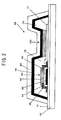
- FIG. 2 is a schematic cross sectional view for showing an organic EL display device P1 related to the present embodiment.
- the organic EL display device P1 includes a film substrate 10, a barrier film 12 formed on the substrate 10, an organic EL element 100 and an organic TFT 50 which are formed on the barrier film 12, an interlayer insulation film 72 which covers the organic TFT 50, a negative electrode 18 of the organic EL element 100 which covers the interlayer insulation film 72, and a protection film 20 which covers a surface of the negative electrode 18 to protect the organic EL element 100 and the organic TFT 50 from erosion.
- the barrier film 12 is formed on the substrate 10.
- the organic EL element 100 and the organic TFT 50 are disposed in parallel on the barrier film 12.
- the interlayer insulation film 72 is disposed on the left side of the drawing sheet in the organic EL element 100 described later and formed to reach from the top of the below described positive electrode 14 of the organic EL element 100 to the surface of the organic TFT 50 and further to a portion contact with the negative electrode 18.
- an interlayer insulation film 74 for insulating the positive electrode 14 and the negative electrode 18 is disposed on the right side of the drawing sheet in the organic EL element 100 described later and formed to reach from the top of the positive electrode 14 of the organic EL element 100 to a portion contact with the negative electrode 18.
- the negative electrode 18 of the organic EL element 100 described later is extended on the interlayer insulation film 72 and the interlayer insulation film 74 to cover the surface of the insulation films.
- the negative electrode 18 is a conductive layer and functions as a protection layer for protecting the organic TFT 50 from at least one of electromagnetic wave and particle beam.
- the protection film 20 covers the surface of the negative electrode 18 to protect the organic EL element 100 and the organic TFT 50 from outside erosion.
- resins used for a variety of substrates may include thermoplastic resin, thermoset resin, polycarbonate, polymethylmethacrylate, polyarylate, polyethersulfone, polysulfone, polyethyleneterephthalate polyester, polypropylene, cellophane, polycarbonate, acetylcellulose, polyethylene, polyvinyl chloride, polystyrene, polyamide, polyimide, polyvinylidene chloride, polyvinyl alchohol, ethylene-vinyl acetate copolymer saponifiables, fluorine resin, chlorinated rubber, ionomer, ethylene acrylic copolymer, ethylene acrylic ester copolymer, etc.
- substrates may be glass substrates or substrates laminated with glass and plastic, or substrate surfaces may be coated with an alkali barrier film or a gas barrier film. Further, in the case of a top emission type for irradiating light from the opposite side of the substrate, the substrate 10 may not be necessarily transparent.
- the barrier film 12 may not be necessarily formed, it is preferable to form the barrier film because erosion caused by moisture and oxygen generated from the substrate side can be prevented. Materials may be appropriately selected to form the barrier film 12.
- the barrier film 12 may be of multilayer structure or single layer structure, and inorganic film or organic film. However, it is preferable to include the inorganic film because it improves barrier performance to prevent erosion by moisture and oxygen.
- nitride film, oxide film, carbon film, or silicon film may be employed. More particularly, silicon nitride film, silicon oxide film, silicon oxide nitride film, or diamond like carbon (DLC) film, amorphous carbon film are cited. That is, cited are nitride such as SiN, AlN, GaN, oxides such as SiO, Al 2 O 3 , Ta 2 O 5 , ZnO, GeO, oxide nitride such as SiON, carbide nitride such as SiCN, metal fluoride, and metal film.
- nitride film, oxide film, carbon film, or silicon film may be employed. More particularly, silicon nitride film, silicon oxide film, silicon oxide nitride film, or diamond like carbon (DLC) film, amorphous carbon film are cited. That is, cited are nitride such as SiN, AlN, GaN, oxides such as SiO, Al 2 O 3 , Ta 2 O 5 , ZnO
- organic film cited are, for example, furane film, pyrrole film, thiophene film, polyparaxylene film epoxy resin, acrylic resin, polyparaxylene, fluorine polymer (perfluoroolefin, perfluoroether, tetrafluoroethylene, chlorotrifluoroethylene, dichlorodifluoroethylene, etc.), or polymerized film such as metal alkoxide (CH 3 OM, C 2 H 5 OM, etc.), polyamide precursor, peril compound, etc.
- fluorine polymer perfluoroolefin, perfluoroether, tetrafluoroethylene, chlorotrifluoroethylene, dichlorodifluoroethylene, etc.
- polymerized film such as metal alkoxide (CH 3 OM, C 2 H 5 OM, etc.), polyamide precursor, peril compound, etc.
- a laminated structure including two and more types of materials a laminated structure including inorganic protection film, silane coupling layer, resin sealing film, a laminated structure including a barrier layer formed of inorganic material and a cover layer formed of organic material, a laminated structure including a compound of organics and semiconductor or metals such as Si-CXHY, and inorganic, a laminated structure in which organic and inorganic films are alternately laminated, a laminated structure in which SiO 2 or Si 3 N 4 is layed on a Si layer, etc.
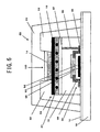
- FIG. 3 is an enlarged view showing vicinity of the organic EL element 100 of the organic EL display device P1.
- the organic EL element 100 is configured in such that the positive electrode 14, the organic solid layer 16, and the negative electrode 18 are laminated in order from the barrier film 12 side.
- the lower electrode may be negative and the upper electrode may be positive and at least either one is required to be transparent.
- the layer having such an energy level to easily inject electron holes may be used and a transparent electrode such as ITO (indium tin oxide) may be used.
- ITO indium tin oxide
- the transparent conductive material such as ITO is formed into a thickness of e.g. 150 nm by spattering or others.
- a zinc oxide (ZnO) film, IZO (indium zinc oxide), copper iodide, etc. may be employed instead of ITO.
- the organic solid layer 16 is configured in such that an electron hole injection layer 162, an electron hole transport layer 164, a luminescent layer 166, an electron transport layer 167, and an electron injection layer 168 which are laid in order from the positive electrode 14 side.
- the electron hole injection layer 162 is provided between the positive electrode 14 and the luminescent layer 166 and is a layer for promoting electron holes injection from the positive electrode 14.
- the driving voltage of the organic EL element 100 can be lowered with electron hole injection layer 162.
- the electron hole injection layer 162 facilitates to stabilize electron hole injection so as to increase longevity of elements, and facilitates to coat convex-concave surfaces such as projection formed on the surface of the positive electron 14 so as to decrease element defects.
- Materials of the electron hole injection layer 162 may be appropriately selected to meet the requirement that its ionized energy is between the work function of the positive electrode 14 and the ionized energy of the luminescent layer 166.
- TPTE triphenylamine tetramer
- copper phthalocyanine may be used.
- the electron hole transport layer 164 is provided between the electron hole injection layer 162 and the luminescent layer 166, and is a layer for promoting electron hole transportation and has a function to appropriately transport electron holes to the luminescent layer 166.
- Materials of the electron hole transport layer 164 may be appropriately selected to meet the requirement that its ionized energy is between the electron hole injection layer 162 and the luminescent layer 166.
- TPD triphenylamine derivative
- TPD triphenylamine derivative
- the luminescent layer 166 is a layer to recombine the electron hole thus transported and the electron described later which is transported as well to emit fluorescence or phosphorescence. Materials of the luminescent layer 166 may be appropriately selected so as to satisfy the characteristics to correspond to the above-mentioned luminous mode.
- tris(8-quinolinorate) aluminum complex (Alq), bis(benzoquinolirate) beryllium complex (BeBq), tri(dibenzoyl methyl) phenanthroline europium complex (Eu(DBM)3(Phen)), ditholilvinylbiphenyl (DTVBi), ⁇ -conjugated polymers such as poly(p-phenylenevinylene), and polyalkylthiophene may be used.
- Alq 3 almiqunolinol complex
- Alq 3 almiqunolinol complex
- a phosphorescence emission type element electrons and electron holes are injected into the phosphorescence layer 166 from the negative electrode 18 and the positive electrode 14 respectively to be recombined, and therefore, the recombined energy is supplied to a dopant material thorough a host material to emit phosphorescence.
- dopant-generated red luminescence is obtained in this phosphorescence-emission-type organic EL element.
- the host material having a luminescence emission function related to the present invention also emits light, so that added color luminescence of luminescence colors of the host material and the dopant material is obtained.
- white luminescence synthesized by blue and red can be ejected in this organic EL element.
- the electron transport layer 167 is provided between the luminescent layer 166 and the electron injection layer 168 and has a function to promote electron transportation into the luminescent layer 166.
- Materials of the electron transport layer 167 may be appropriately selected so as to meet the requirement that electron affinity should be between the luminescent layer 166 and the electron injection layer 168.
- almiquinolinol complex Alq 3
- Alq 3 almiquinolinol complex
- the electron injection layer 168 is provided between the negative electrode 18 and the electron transport layer 167 and has a function to promote electron injection from the negative electrode 18.
- Materials of the electron injection layer 168 may be appropriately selected to meet the requirement that electron affinity should be between work function of the negative electrode 18 and an electron affinity of the luminescent layer 166.
- a thin film e.g. 0.5 nm
- LiF lithium fluoride
- Li 2 O lithium oxide
- etc. may be employed for the electron transport layer 168.
- Each layer forming the organic solid layer 16 is generally made of organic materials, particularly made of low-molecular organics and made of high-molecular organics.
- the organic solid layer made of low-molecular organics is generally formed by dry process (vacuum process) such as vapor deposition method, and the organic solid layer made of high-molecular organics may be generally formed by wet process such as spin coating method, plate coating method, dipping method, spraying method and printing method.
- organic materials used for each layer forming the organic solid layer 16 for example, PEDOT, polyaniline, poly(p-phenylenevinylene) derivative, polythiophene derivative, poly(p-phenylene) derivative, polyalkylphenilane, polyacetylene derivative, etc. are cited.
- the organic solid layer 16 including the electron hole injection layer 162, the electron hole transport layer 165, the luminescent layer 166, the electron transport layer 167, and the electron injection layer 168 is cited in the present embodiment, the organic solid layer is not limited to this configuration and the configuration may include at least the luminescent layer 166.
- a single-layer structure of the luminescent layer a double-layer structure such as electron hole transport layer/luminescent layer, luminescent layer/electron transport layer, and a triple-layer structure of electron hole transport layer/luminescent layer/electron transport layer, and further a multiple-layer structure comprising an electric charge (electron hole, electron) injection layer may be included depending on characteristics of employed organic materials, etc.
- an electron hole blocking layer may be provided between the luminescent layer 166 and the electron transport layer 167 in the organic solid layer 16.
- the electron holes possibly penetrate through the luminescent layer 166 into the negative electrode 18.
- the electron hole blocking layer may be provided to prevent electron holes from flowing out of the luminescent layer 166 to the electron transport layer 167.
- materials having low work function or low electron affinity may be selected to enhance electron injection into the organic solid layer 16.
- alloy type mixed metal
- Mg:Ag alloy and Al:Li alloy may be preferably used.
- the negative electrode 18 may be formed of metal materials such as Al, Mg, and Ag which are vacuum-evaporated into thickness of e.g. 150 nm.
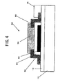
- FIG. 4 is an enlarged view for showing vicinity of an organic TFT 50 of the organic EL display device P1.
- the organic TFT 50 has a gate electrode 52 which is formed on the barrier film 12 from the side of the barrier film 12 and a gate insulation film 54 formed to cover the surface of the gate electrode 52.
- An organic semiconductor layer 56 is formed on the gate insulation film 54, a source electrode 58 is formed on the left end side, and a drain electrode 60 is formed on the right end side.
- the drain electrode 60 is electrically connected with the positive electrode 14 of the organic EL element 100.
- the source electrode 58 and the drain electrode 60 are provided separately from each other, the organic semiconductor layer 56 is disposed between the source electrode 58 and the drain electrode 60, the source electrode 58, the drain electrode 60 and the organic semiconductor layer 56 are arranged so as to oppose the gate electrode 52 through the gate insulation film 54.
- materials of the gate electrode 52 preferable may be metals capable of being anodized and simple substances or their alloys of Al, Mg, Ti, Nb, Zr, etc.
- the material is not limited to those.
- materials having sufficient conductivity may be included, and metal single substances, lamination or their compounds such as, for example, Pt, Au, W, Ru, Ir, Al, Sc, Ti, V, Mn, Fe, Co, Ni, Zn, Ga, Y, Zr, Nb, Mo, Tc, Rh, Pd, Ag, Cd, Ln, Sn, Ta, Re, Os, Tl, Pb, La, Ce, Pr, Nd, Pm, Sm, Eu, Gd, Tb, Dy, Ho, Er, Tm, Yb, Lu, etc. may be included.
- metal oxides such as ITO and IZO or organic conductive materials containing conjugated polymer compounds such as, polyaniline, polythiophene, and polypyrole may be used.
- a general method for forming a wiring pattern of the gate electrode 52 on the substrate 10 may be a manufacturing method of the gate electrode 52a. Although a spattering method, CVD method and others may be cited, the methods are not limited to those and appropriate methods may be appropriately used. For example, general methods for forming thin film such as film vacuum evaporation, ion plating, sol-gel method, spin coating method, spraying method, and CVD may be also possible.
- a surface of a material used as one of the gate electrode 52 may be preferably anodized to form the gate insulation film 54.
- the film is not limited to those but either of inorganic materials and organic materials may be used.
- metal oxides including LiOx, LiNx, NaOx, KOx, RbOx, CsOx, BeOx, MgOx, MgNx, CaOx, CaNx, SrOx, BaOx, ScOx, YOx, YNx, LaOx, LaNx, CeOx, PrOx, NdOx, SmOx, EuOx, GdOx, TbOx, DyOx, HoOx, ErOx, TmOx, YbOx, LuOx, TiOx, TiNx, ZrOx, ZrNx, HfOx, HfNx, ThOx, VOx, VNx, NbOx, TaOx, TaNx, CrOx, CrNx, MoOx, MoNx, WOx, WNx, MnOx, ReOx, FeOx, FeNx, RuOx, OsOx,
- the insulation film is not limited to metal oxides, but may be sulfide such as FeS, Al 2 S 3 , MgS, and ZnS, fluoride such as LiF, MgF 2 , and SmF 3 , chloride such as HgCl, FeCl 2 , CrCl 3 , bromide such as AgBr, CuBr, MnBr 2 , iodide such as PbI 2 , CuI, FeI 2 , and metal oxide nitride such as SiAlON.
- metals and metal compounds may be organic materials such as polymer-based materials including polyimide, polyamide, polyester, polyacrylate, epoxy resin, phenol resin, and polyvinyl alcohol.
- Materials may not be limited specifically, but may be applicable for the source electrode 58 and/or the drain electrode 60 as long as they have enough conductivity.
- materials include metal single substances, lamination or their compounds such as Pt, Au, W, Ru, Ir, Al, Sc, Ti, V, Mn, Fe, Co, Ni, Zn, Ga, Y, Zr, Nb, Mo, Te, Rh, Pd, Ag, Cd, Ln, Sn, Ta, Re, Os, Tl, Pb, La, Ce, Pr, Nd, Pm, Sm, Eu, Gd, Tb, Dy, Ho, Er, Tm, Yb, Lu, etc. may be included.
- metal oxides such as ITO and IZO, or organic conductive materials containing conjugated polymer compounds of such as polyaniline, polythiophene, and polypyrole may be used.
- the source electrode 58 and the drain electrode 60 may be manufactured by general methods.
- a spattering method, a CVD method, etc. are cited but not specifically limited. Appropriate methods may be appropriately employed.
- general methods for forming thin films including vacuum evaporation method, ion plating, sol-gel method, spraying method, spin coating method, CVD, and lift-off may be applicable.
- Materials of the organic semiconductor 56 may be organic materials such as pentacene having semiconductor property but not specifically limited. Used are, for example, phthalocyanine-based derivative; naphthalocyanine-based derivative; azo compound-based derivative; perylene-based derivative; indigo-based derivative; quinacridone-based derivative; polycyclic quinon-based derivative such as anthraquinone; cyanine derivative; fullerene derivative; or nitrogen-containing cyclic compound derivatives including indole, carbazole, oxazole, inoxazole, thiazole, imidazole, pyrazole, oxaadiazole, pyrazoline, thiazole, and triazole; hydrazine derivative; triphenylamine derivative; triphenylmethane derivative; quinine compound derivative including stilbene, anthraquinonediphenoquinone, etc.; and cyclic aromatic compound derivative including anthracene, pyrene, phenanthrene,
- polymers in which carbon-based conjugated structure is alternately chained with oligosilane such as disilanylene carbon-based conjugated polymer structure such as polysilane and disilanyleneallylene polymer, (disilanylene)ethenylene polymer, and (disilanylene)ethynylene polymer.
- polymer chain made of inorganic element such as phosphorous base and nitrogen base, polymers coordinated with aromatic ligand of polymer chain such as phthalocyanate polysiloxane, polymer in which perylene such as perylenetetracarboxylic acid is condensed by heat treatment, ladder-type polymers which are obtained by heat-treating polyethylene derivative having cyano group such as polyacrylonitrile, and complex materials in which provskite is intercalated with organic compound.
- a vacuum evaporation method, etc. may be cited but not specifically limited. Appropriate methods may be appropriately employed. For example, general methods for forming thin films including ion plating, sol-gel method, spraying method, and spin coating method may be applicable.
- the interlayer insulation film 72 and the interlayer insulation film 74 may be formed simultaneously or individually. Materials forming each interlayer insulation film may not be specifically limited and material type may be different from each other. And the interlayer insulation film 74 may be appropriately omitted.
- materials forming the interlayer insulation films may not be specifically limited, either of inorganic materials and organic materials may be used.
- metal oxides including LiOx, LiNx, NaOx, KOx, RbOx, CsOx, BeOx, MgOx, MgNx, CaOx, CaNx, SrOx, BaOx, ScOx, YOx, YNx, LaOx, LaNx, CeOx, PrOx, NdOx, SmOx, EuOx, GdOx, TbOx, DyOx, HoOx, ErOx, TmOx, YbOx, LuOx, TiOx, TiNx, ZrOx, ZrNx, HfOx, HfNx, ThOx, VOx, VNx, NbOx, TaOx, TaNx, CrOx, CrNx, MoOx, MoNx, WOx, WNx, MnOx, Li
- a method manufacturing interlayer insulation films may be a method manufacturing without emitting at least one of electromagnetic wave and particle beam, specifically particle beam and ray having shorter wavelength thanvisible ray, so as to prevent the organic TFT 50 from damage.
- general methods for forming thin film such as sol-gel method, spin coating method, spraying method, vacuum evaporation method may be also possible.
- the conductive layer is the negative electrode 18 which is the upper electrode of the organic EL element 100.
- the negative electrode 18 which is the upper electrode of the organic EL element 100 is extended to cover the surface of the interlayer insulation film 72 and protect the organic TFT from at least one of electromagnetic wave and particle beam.
- Electromagnetic waves are to cause damage to layers forming the organic TFT, and they are for example infrared ray, visible ray, and rays having shorter wavelength than visible ray.
- particle beams are to cause damage to layers forming the organic TFT, and they are for example alpha ray, beta ray, and neutron ray.
- to protect the organic TFT from at least one of the electromagnetic wave and the particle beam is a concept that includes protecting the organic TFT from at least one of electromagnetic wave and particle beam by at least one mode of shielding, absorption, and reflection.
- the conductive layer is not limited as long as the layer has conductivity.
- the conductive layer having conductivity is preferable because the conductive layer is convertible with the electrode of the organic EL element 50 or has characteristics to discharge shielding against electromagnetic wave and/or particle beam, heat, and electric charge.
- the conductive layer is formed of conductive coating material.
- the conductive coating material may be any one that can apply conductivity, and a coating material dispersing conductive powder to binder resin, and a coating material made of organic metal compound and a coating material made of organic conductive resin may be used.
- a type of coating material using non-solvent may be possible as well as material using solvent.
- binder resin used may be a mixture of one or more types of cellulose-based resin including nitrocellulose, acetyl cellulose, cellulose acetate propionate; acrylic resin including poly(metha)butyl acrylate; polyvinyl chloride acetate copolymer; polyester resin; polyvinyl butyral; and polyurethane resin.
- cellulose-based resin including nitrocellulose, acetyl cellulose, cellulose acetate propionate
- acrylic resin including poly(metha)butyl acrylate
- polyvinyl chloride acetate copolymer polyester resin
- polyvinyl butyral polyurethane resin
- conductive powder used may be metal particles including gold, silver, copper, stainless, aluminum, zinc, tin indium, antimony, and nickel; conductive pigment including carbon black, and black lead; metal oxides including zinc oxide, tin oxide, indium oxide, and titan oxide; and fine carbon fiber including carbon nanotube, and fullerenes.
- Shapes of the conductive powder are not limited specifically but shapes of globe, ellipsoid, scale, and needle may be used.
- organic metal compound used may be organic silver compounds including methyl silver, butyl silver, and phenyl silver; and organic metal compounds including monoalkyl(aryl) gold derivative (ethyl dibromide gold, dichloride phenyl gold, etc.), dialkyl gold derivative, and trialkyl gold derivative.
- organic conductive resin used may be organic compounds having pi-conjugated system combination including polyaniline and polythiophene.
- conductive powder, organic metal compound, and organic conductive resin may be used individually or in combination.
- the conductive coating material may be added with other additives, for example, curing agent, leveling agent, antifoaming agent, and viscosity modifier.
- the conductive layer when the conductive layer is convertible with the negative electrode 18, the process in which they are produced together is easy and preferable. However, this is not limited and they may not be convertible but may be formed in discontinuous manner. Further the conductive layer may be convertible with the positive electrode, and for example, in the case of top emission type, it is preferable to form the conductive layer convertible with the positive electrode in view of derivation.
- particle beam and a visible ray rays having shorter wavelength than visible ray protect at least one of electromagnetic wave to prevent from causing damage to the organic TFT 50. It is more preferable to protect the organic TFT 50 from these short-wavelength rays because they tend to cause more damage to the organic TFT 50 as the wavelength becomes short, such as blue ray, purple ray, ultraviolet ray, and X-ray.
- the conductive layer it is preferable because a color transparent layer or opaque layer having a clearness degree lower than translucence is easy to protect the organic TFT 50 from electromagnetic wave.
- this is not limited, but color having higher absorption of electromagnetic wave and/or particle beam is preferable, particularly black is preferable. Transparent and colorless may be possible as long as the layer contains light absorbing agent and particle beam absorbing agent.
- the conductive layers having metal luster of metals such as Al, specularity, electromagnetic reflexivity are preferable in view of protection for the organic TFT and light extract effect of the organic EL element.
- metal luster may be provided by print ink of metallic tone such as silver and gold, which is added with metal pigment such as aluminum paste and aluminum powder.
- the method for forming the conductive layer preferable is a method to emit particle beam and electromagnetic waves as little as possible so not to cause damage to the organic TFT 50.
- general methods for forming thin films such as methods of ion plating, sol-gel, spraying, spin coating, and vacuum evaporation may be possible.
- the protection film 20 may have a multilayer structure or a single layer structure and may be an inorganic film or an organic film.
- the film including inorganic film is preferable because erosion due to moisture and oxygen increases barrier properties.
- nitride film, oxide film, carbon film, or silicon film may be employed.
- silicon nitride film, silicon oxide film, silicon oxide nitride film, or diamond like carbon (DLC) film, amorphous carbon film are cited. That is, cited are nitride such as SiN, AIN, and GaN; oxides such as SiO, Al 2 O 3 , Ta 2 O 5 , ZnO, and GeO; oxide nitride such as SiON; carbide nitride such as SiCN; metal fluoride compound; and metal film.
- organic film cited are, for example, furane film, pyrrole film, thiophene film, polyparaxylene film, epoxy resin, acrylic resin, polyparaxylene, fluorine polymer (perfluoroolefin, perfluoroether, tetrafluoroethylene, chlorotrifluoroethylene, dichlorodifluoroethylene, etc.), or polymerized film such as metal alkoxide (CH 3 OM, C 2 H 5 OM, etc.), polyimide precursor, perylene-based compound, etc.
- fluorine polymer perfluoroolefin, perfluoroether, tetrafluoroethylene, chlorotrifluoroethylene, dichlorodifluoroethylene, etc.
- polymerized film such as metal alkoxide (CH 3 OM, C 2 H 5 OM, etc.), polyimide precursor, perylene-based compound, etc.
- the protection film 20 cited are a laminated structure composed of not less than two kinds of materials, a laminated structure composed of inorganic protection film, silane coupling layer, resin sealing film, a laminated structure composed of a barrier layer formed of an inorganic material and a cover layer formed of an organic material, a laminated structure composed of a compound of organics and semiconductor or metals such as Si-CXHY, and inorganic, a laminated structure in which inorganic and organic films are alternately laminated, a laminated structure in which SiO 2 or Si 3 N 4 is laid on a Si layer, etc.
- the barrier film 12 and the protection film 20 have a function to mainly protect the organic EL element 100 from outside air (such as oxygen) and moisture by the component inorganic film which mainly blocks outside air (such as oxygen) and moisture.
- the barrier film 12 has a main function to block outside air (such as oxygen) and moisture from the side of the substrate 10 and the protection film 20 has a main function to block a portion not covered with the organic EL element 100 from outside air (such as oxygen) and moisture.
- the component organic film fills in pinholes and surface unevenness formed in the inorganic film to level the surface. It also functions to reduce film stress of the inorganic film.
- Methods for manufacturing the protection film 20 may include spattering method and CVD method. However, they are not limited but appropriate methods may be used appropriately. For example, general methods for forming thin film such as vacuum evaporation, ion plating, sol-gel method, spraying method, spin coating method, and CVD may be also possible.
- Luminescence mode of the above-mentioned organic EL display device P1 will be described.
- the electron holes are supplied from the source electrode 58 to the drain electrode 60 through the gate insulation film 54.
- the electrode holes are transferred to the positive electrode 14 of the organic EL element 100 through the drain electrode 60.
- the electron holes are transported from the positive electrode 14 to the electron hole injection layer 162 of the organic solid layer 16.
- the electron holes thus transported are injected into the electron hole transport layer 164.
- the electron holes thus injected into the electron hole transport layer 164 are transported into the luminescent layer 166.
- the organic EL element 100 electrons are injected from the negative electrode 18 into the electron injection layer 168 of the organic solid layer 16. The electrons thus injected are transported into the luminescent layer 166 through the electron transport layer 167.
- the electron holes and electrons thus transported are recombined in the luminescent layer 166.
- Luminescence due to EL is emitted by energy generated during the recombination. This luminescence is derived toward outside through the electron hole transport layer 164, the electron hole injection layer 162, the positive electrode 14, the barrier film 12 and the substrate 10 in order respectively so that the luminescence becomes visible.
- the interface between the negative electrode layer 18 and the electron injection layer 168 becomes a reflecting surface on which they are reflected and proceed to the side of the positive electrode 14 and penetrate the substrate 10 to eject outside. Therefore, when the organic EL element having the above configurations is employed for displays, the side of the substrate 10 becomes a viewing surface.
- a manufacturing method in which the organic EL element emitting each color light of RGB are separately coated (separate coating method), a method of combination of an organic EL element emitting single white color and a color filter (color filter method), a method of combination of an organic EL element emitting a single color such as blue or white and a color converting layer (color converting method), and a method in which a single color organic EL element realizes multiple luminescence by irradiating electromagnetic wave to the organic luminescent layer and others (photo bleaching method).
- a manufacturing method in which the organic EL element emitting each color light of RGB are separately coated (separate coating method)
- color filter method a method of combination of an organic EL element emitting single white color and a color filter
- color converting method a method of combination of an organic EL element emitting a single color such as blue or white and a color converting layer
- photo bleaching method a method in which a single color organic EL element realizes multiple luminescence by ir
- the organic TFT can be protected more from particle beam and electromagnetic waves causing damage to the organic TFT. Therefore, it is more reliable even though using other manufacturing process in which the organic EL display device P1 generating particle beam and electromagnetic waves causing damage to the organic TFT and using long by consumers.
- a method of manufacturing the organic EL display device P1 shown in FIG. 2 will be described.
- the barrier film 12 is formed and then the organic TFT 50 and the positive electrode 14 of the organic EL element 100 are formed.
- the drain electrode 60 of the organic TFT 50 and the positive electrode 14 of the organic EL element 100 are formed so as to contact with each other for electrical conduction.
- the interlayer insulation film 72 located on the left end side of the sheet of the organic EL element 100 is formed so as to cover the surface of the organic TFT 50.
- the interlayer insulation film 74 located on the right end side of the organic EL element 100 is formed so as to cover the positive electrode 14.
- the negative electrode 18 and the organic solid layer 16 of the organic EL element 100 are formed.
- the negative electrode 18 is formed to extend to a top of the interlayer insulation film so as to cover the organic TFT 50.
- the protection film 20 is formed so as to cover the surface to manufacture the organic EL display device P1.
- the negative electrode 18 which is a conductive layer protects from the particle beam and electromagnetic waves causing damage to these organic TFT 50, so that the organic EL display device P1 including the less-damaged organic TFT 50 can be provided.
- applicable printing method may include gravure coating, gravure reverse coating, comma coating, die coating, lip coating, cast coating, roll coating, air knife coating, mayer bar coating, extrusion coating, offset, ultraviolet cure offset, flexo, hole plate, silk, curtain flow coating, wire bar coating, reverse coating, gravure coating, kiss coating, blade coating, smooth coating, spray coating, flow coating, and brush coating.
- lower layer and its upper layer may be double laid in wet condition and then dried, as well as the lower layer is formed in dry condition and then coated over.
- FIG. 5 shows the organic EL display device P2 in Embodiment 1 related to the present embodiment. Since the same numeral references hereinafter are similar to those of the above-mentioned embodiment, description is omitted.
- An organic EL element 100 having a top emission structure is disposed on the organic TFT 50, and the organic EL element 100 and the organic TFT 50 are covered with the protection film 20.
- the negative electrode 18 of the organic EL element is formed so as to cover the interlayer insulation film on the organic TFT.
- the organic semiconductor layer 56 of the organic TFT 50 is made of n-type organic semiconductor.
- the drain electrode 60 and the negative electrode 18 are electrically connected by the through-hole 80 which is a charge transport path provided in the interlayer insulation film 72.
- the barrier film 12 is formed on the substrate 10 to produce the organic TFT 50.
- the interlayer insulation film 72 is formed so as to cover the surface of the organic TFT 50 to produce a through hole 80.
- the negative electrode 18 is formed.
- the insulation film 22 for protecting from short circuit between the negative electrode and the positive electrode is formed on the end of the organic EL element.
- the organic EL element 100 is formed.
- the protection film 20 is formed so as to entirely cover the organic EL element and the organic TFT to produce the organic EL display device P2.
- the negative electrode 18 which is a conductive layer protects from at least one of the particle beam and electromagnetic waves causing damage to these organic TFT 50, so that the organic EL display device P2 including the less-damaged organic TFT 50 can be provided.
- FIG. 6 shows the organic EL display device P3 of the other embodiment 2 related to the present embodiment.
- the organic TFT 59 for driving is arranged on the organic TFT 50 for switching, the top-contact-type organic EL element 100 is arranged on the organic TFT 59, and the organic EL element 100, the organic TFT 50, and the organic TFT 59 are covered with the protection film 20.
- the driving transistor is a static induction transistor (SIT) as in FIG. 6, the drain electrode of the organic TFT 59 is made to entirely cover the organic TFT 50 and the organic TFT 59.
- the semiconductor layer of the organic TFT 50 and the organic TFT 59 is a n-type organic semiconductor.
- the organic TFT 59 is composed of the source electrode 57/gate electrode 51/drain electrode (the positive electrode 14 of the organic EL element 100).
- the drain electrode 60 and the source electrode 57 of the organic TFT 59 are electrically connected by the through hole 80 which is an electron hole transport path provided in the interlayer insulation film 72.
- the barrier film 12 is formed on the substrate 10 to produce the organic TFT 50 for switching.
- the interlayer insulation film 72 is formed so as to cover the surface of the organic TFT 50 to produce the through hole 80.
- the organic TFT 59 for driving is formed.
- the insulation film 22 for protecting the end of the organic EL element from short circuit is formed.
- the organic EL element 100 is formed on the organic TFT 59.
- the protection film 20 is formed so as to entirely cover the organic EL element and the organic TFT to produce the organic EL display device P3.
- the positive electrode 14 which is a conductive layer protects from the particle beam and electromagnetic waves causing damage to these organic TFT 50, so that the organic EL display device P3 including the less-damaged organic TFT 50 can be provided.
- the negative electrode 18 or the drain electrode of the organic TFT 59 has reflexivity to at least one of the electromagnetic wave and the particle beam and is preferable for protecting from at least one of the electromagnetic wave and the particle beam causing damage to the organic TFT 50.
- the organic EL display device including the organic EL element is shown but this is not limited. Even the case of the organic transistor driving others than the organic EL element, a configuration of protecting at least one of the electromagnetic wave and the particle beam by the conductive layer according to the present embodiment is applicable. That is, in the above-mentioned embodiment, the organic EL element may be replaced with an other driving element driven by the organic transistor or the driving element such as the organic EL element may be omitted and formed as a single organic transistor. Regardless of direction and indirection, the conductive layer may be formed on the surface of them and the protection film may be formed on the conductive layer.
- Such an organic transistor may be applied for displays in general, e.g. LCD displays, electrophoretic displays, electronic paper, and toner displays.
- a Ta film as the gate electrode is formed on a plastic film substrate by a sputtering method at thickness of 2000 ⁇ to form wiring pattern. This is anodized to obtain the gate insulation film Ta 2 O 5 . Further, Au film of 100nm thickness having an adhesion layer of 5nm Cr film is formed by lift-off as source and drain electrodes. And subsequently ITO as a positive electrode of the organic EL element is formed so as to contact with the drain electrode of the organic TFT. And then pentacene is film-formed by a vacuum evaporating method as the organic semiconductor layer. Then the interlayer insulation film PVA (polyvinyl alcohol) having sufficient thickness is produced so as to entirely cover the organic TFT.
- PVA polyvinyl alcohol
- This insulation film is subjected by patterning so as to cover the end portion of the organic EL element for protecting the organic EL element from short circuit of the positive electrode and negative electrode.
- the negative electrode Al is also film-formed on the organic TFT as well as the organic EL element.
- SiNx is film-formed by plasma CVD method as a protection film of the organic layer for protecting from moisture and gas from outside.
- interlayer insulation film on the organic TFT and the negative electrode of the organic EL element are both not film-formed panels and the remaining is similar with the embodiment.
- the organic EL display device of the embodiment can obtain excellent semiconductor property (mobility, on-off property) compared with the comparative example.
Landscapes
- Engineering & Computer Science (AREA)
- Microelectronics & Electronic Packaging (AREA)
- Electroluminescent Light Sources (AREA)
- Thin Film Transistor (AREA)
- Devices For Indicating Variable Information By Combining Individual Elements (AREA)
Abstract
Description
- The present invention relates to an organic EL display device, a method of manufacturing an organic EL display device, an organic transistor, and a method of manufacturing an organic transistor.
- An organic transistor is used for variety of applications. For example, it is used as a means for driving organic EL elements in the organic EL display devices.
- The organic EL element is provided with electrodes on a substrate and an organic solid layer having at least a luminescent layer between the electrodes, wherein electrons and electron holes are injected into the luminescent layer in the organic solid layer from the electrodes on both sides to emit light in the organic luminescent layer and high intensity luminescence is available. Further it features wide selection of luminescent colors because luminescence of the organic compound is employed. Therefore, it is expected as a light source and an organic EL display device. Particularly, since the organic EL display device generally has high visual field, high contrast, high-speed responsibility, excellent visibility, thin shape and light weight, it is expected as a low-power-consumption flat panel display.
- The organic EL display device includes pixels having at least a positive electrode, an organic luminescent layer, a negative electrode and a transistor for lighting and controlling the organic EL element. There are two types of driving organic EL display devices - a passive matrix method and an active matrix method. In the passive matrix method, the organic EL elements arranged in a matrix shape are driven from the outside with a stripe-like scan electrode and data electrode (signal electrode) which are perpendicular to each other. In the active matrix method, a driving element, a switching element formed of thin film transistor (also refereed to as TFT hereinafter) and a memory element in every pixel are provided to light the organic EL element.
- With the increasing number of pixels, generally, the active matrix method for driving the organic EL element with TFT (Thin Film Transistors) is considered more advantageous for the organic EL display device than the passive matrix method is. This is because with the passive matrix method in which the organic EL element of each pixel is lit during the period a scanning electrode is selected and the period for lighting the organic EL element tends to decrease to lower average luminance as the number of pixels increases. On the contrary with the active matrix method, each pixel has a memory element and a switching element formed of TFT, lighting state of the organic EL element is kept, high luminance, high efficiency and long-life operation are possible, therefore the active matrix method tends to be advantageous for displays of high resolution and enlarged size.
- Use of the organic TFT for TFT may lead to reduction of costs and environment load. Further since the organic TFT can be produced at low process temperature, it may be produced on film substrates, and therefore, flexible displays are expected to be realized.
- With regard to organic EL elements and organic TFTs, they are susceptible to erosion due to moisture and oxygen in the air, in the presence of which there may be occurrence of deterioration such as dark-spot and element short. A means for protecting elements from erosion due to moisture and oxygen in the air is necessary to protect from this deterioration. At present, a method in which elements are entirely sealed with cover glass and can packages in the atmosphere of dry nitrogen and argon gas is employed.
- However, production costs of this sealing method using these glass and cans are high and there is limitation to decrease in element thickness. Then, a configuration in which organic EL elements and organic TFT are covered with protection films having a moisture-prevention function without using glass and can packages is proposed in the
patent reference 1 described below. - FIG. 1 shows an organic EL display device PA related to the prior art. The organic EL display device PA has a
substrate 10, abarrier film 12 formed on thesubstrate 10, anorganic EL element 100 andorganic TFT 50 formed on thebarrier film 12, a protection film (passivation film) 20 covering theorganic EL element 100 and theorganic TFT 50. Patent reference 1:Japanese Unexamined Patent Application Publication No. 2003-255857 - However, when the protection film is film-formed by e.g. vacuum processing of a CVD method, the organic layer and others forming the organic TFT are damaged by particle beam and electromagnetic waves which are generated from plasma produced at the time of film forming, so that performance of the organic TFT may be deteriorated.
- Further, after manufacturing the protection film, the organic layer and others forming the organic TFT are damaged by at least one of electromagnetic wave and particle beam which are generated when users use and in a step of manufacturing, so that performance of the organic TFT may be deteriorated.
- The present invention is made in view of the above object and main purposes of the invention are to provide an organic EL display device having organic transistor-performance which is less deteriorated, a method of manufacturing the organic EL display device, an organic transistor and a method of manufacturing the organic transistor.
- According to a first aspect of the present invention, an organic EL display device includes an organic EL element which is provided with at least a positive electrode, an organic luminescent layer and a negative electrode, and an organic transistor for driving the organic EL element, and the organic EL display device further comprises a protection film for covering the organic transistor to protect at least the organic transistor, wherein a conductive layer having conductivity is formed in respect of between the protection film and a surface of the organic transistor, and an insulation film for insulating the conductive layer and the surface of the organic transistor, formed on the side of the surface of the organic transistor but the conductive layer.
- According to a ninth aspect of the present invention, a method of manufacturing an organic EL display device, which includes an organic EL element provided with at least a positive electrode, an organic luminescent layer and a negative electrode, and an organic transistor driving the organic EL element, comprises steps of:
- forming an insulation film for insulating the conductive layer and the surface of the organic transistor;
- forming a conductive layer on the insulation film; and
- forming a protection film for protecting the organic transistor on the conductive layer.
- According to a fifteenth aspect of the present invention, an organic transistor includes a protection film for covering the organic transistor to protect at least one of the organic transistor and further includes:
- a conductive layer having conductivity, in respect between the protection film and a surface of the organic transistor; and
- an insulation film for insulating the conductive layer and the surface of the organic transistor, formed on the side of the surface of the organic transistor but the conductive layer.
- According to a twenty second aspect of the present invention, a method of manufacturing an organic transistor comprises steps of:
- forming an insulation film for insulating the conductive layer and the surface of the organic transistor;
- forming a conductive layer on the insulation film; and
- forming a protection film for protecting the organic transistor on the conductive layer.
-
- [FIG. 1] A schematic cross sectional view for showing an organic EL display device related to prior art.
- [FIG. 2] A schematic cross sectional view for showing an organic EL display device in the present embodiment.
- [FIG. 3] A schematic enlarged view for showing vicinity of an organic EL element of the organic EL display device in the present embodiment.
- [FIG. 4] A schematic enlarged view for showing vicinity of the organic TFT of the organic EL display device in the present embodiment.
- [FIG. 5] A schematic cross sectional view for showing the organic EL display device in the present embodiment.
- [FIG. 6] A schematic cross sectional view for showing the organic EL display device in the present embodiment.
-
- 10
- Substrate
- 16
- Organic solid layer
- 18
- Negative electrode
- 20
- Protection film
- 50
- Organic TFT
- 72, 74, 76
- Insulation film
- 100
- Organic EL element
- P1, P2, P3, PA
- Organic EL display device
- Embodiments of the present invention will be described with reference to drawings hereinafter. These embodiments are just shown as exemplification to practice the present invention and the present invention is not limited by these embodiments.
- FIG. 2 is a schematic cross sectional view for showing an organic EL display device P1 related to the present embodiment. The organic EL display device P1 includes a
film substrate 10, abarrier film 12 formed on thesubstrate 10, anorganic EL element 100 and anorganic TFT 50 which are formed on thebarrier film 12, aninterlayer insulation film 72 which covers theorganic TFT 50, anegative electrode 18 of theorganic EL element 100 which covers theinterlayer insulation film 72, and aprotection film 20 which covers a surface of thenegative electrode 18 to protect theorganic EL element 100 and theorganic TFT 50 from erosion. - The
barrier film 12 is formed on thesubstrate 10. Theorganic EL element 100 and theorganic TFT 50 are disposed in parallel on thebarrier film 12. Theinterlayer insulation film 72 is disposed on the left side of the drawing sheet in theorganic EL element 100 described later and formed to reach from the top of the below describedpositive electrode 14 of theorganic EL element 100 to the surface of theorganic TFT 50 and further to a portion contact with thenegative electrode 18. And aninterlayer insulation film 74 for insulating thepositive electrode 14 and thenegative electrode 18 is disposed on the right side of the drawing sheet in theorganic EL element 100 described later and formed to reach from the top of thepositive electrode 14 of theorganic EL element 100 to a portion contact with thenegative electrode 18.
Thenegative electrode 18 of theorganic EL element 100 described later is extended on theinterlayer insulation film 72 and theinterlayer insulation film 74 to cover the surface of the insulation films. Thenegative electrode 18 is a conductive layer and functions as a protection layer for protecting theorganic TFT 50 from at least one of electromagnetic wave and particle beam. Theprotection film 20 covers the surface of thenegative electrode 18 to protect theorganic EL element 100 and theorganic TFT 50 from outside erosion. - Materials of the
substrate 10 may be appropriately selected and used. For example, resins used for a variety of substrates may include thermoplastic resin, thermoset resin, polycarbonate, polymethylmethacrylate, polyarylate, polyethersulfone, polysulfone, polyethyleneterephthalate polyester, polypropylene, cellophane, polycarbonate, acetylcellulose, polyethylene, polyvinyl chloride, polystyrene, polyamide, polyimide, polyvinylidene chloride, polyvinyl alchohol, ethylene-vinyl acetate copolymer saponifiables, fluorine resin, chlorinated rubber, ionomer, ethylene acrylic copolymer, ethylene acrylic ester copolymer, etc. Meanwhile resins are not principal ingredient for substrates but substrates may be glass substrates or substrates laminated with glass and plastic, or substrate surfaces may be coated with an alkali barrier film or a gas barrier film. Further, in the case of a top emission type for irradiating light from the opposite side of the substrate, thesubstrate 10 may not be necessarily transparent. - Although the
barrier film 12 may not be necessarily formed, it is preferable to form the barrier film because erosion caused by moisture and oxygen generated from the substrate side can be prevented. Materials may be appropriately selected to form thebarrier film 12.
Thebarrier film 12 may be of multilayer structure or single layer structure, and inorganic film or organic film. However, it is preferable to include the inorganic film because it improves barrier performance to prevent erosion by moisture and oxygen. - As for the inorganic film, for example, nitride film, oxide film, carbon film, or silicon film may be employed. More particularly, silicon nitride film, silicon oxide film, silicon oxide nitride film, or diamond like carbon (DLC) film, amorphous carbon film are cited. That is, cited are nitride such as SiN, AlN, GaN, oxides such as SiO, Al2O3, Ta2O5, ZnO, GeO, oxide nitride such as SiON, carbide nitride such as SiCN, metal fluoride, and metal film.
- As for the organic film, cited are, for example, furane film, pyrrole film, thiophene film, polyparaxylene film epoxy resin, acrylic resin, polyparaxylene, fluorine polymer (perfluoroolefin, perfluoroether, tetrafluoroethylene, chlorotrifluoroethylene, dichlorodifluoroethylene, etc.), or polymerized film such as metal alkoxide (CH3OM, C2H5OM, etc.), polyamide precursor, peril compound, etc.
- As for the
barrier film 12, cited are a laminated structure including two and more types of materials, a laminated structure including inorganic protection film, silane coupling layer, resin sealing film, a laminated structure including a barrier layer formed of inorganic material and a cover layer formed of organic material, a laminated structure including a compound of organics and semiconductor or metals such as Si-CXHY, and inorganic, a laminated structure in which organic and inorganic films are alternately laminated, a laminated structure in which SiO2 or Si3N4 is layed on a Si layer, etc. - FIG. 3 is an enlarged view showing vicinity of the
organic EL element 100 of the organic EL display device P1. Theorganic EL element 100 is configured in such that thepositive electrode 14, the organicsolid layer 16, and thenegative electrode 18 are laminated in order from thebarrier film 12 side. The lower electrode may be negative and the upper electrode may be positive and at least either one is required to be transparent. - For the
positive electrode 14, the layer having such an energy level to easily inject electron holes may be used and a transparent electrode such as ITO (indium tin oxide) may be used. - The transparent conductive material such as ITO is formed into a thickness of e.g. 150 nm by spattering or others. A zinc oxide (ZnO) film, IZO (indium zinc oxide), copper iodide, etc. may be employed instead of ITO.
- The organic
solid layer 16 is configured in such that an electronhole injection layer 162, an electronhole transport layer 164, aluminescent layer 166, anelectron transport layer 167, and anelectron injection layer 168 which are laid in order from thepositive electrode 14 side. - The electron
hole injection layer 162 is provided between thepositive electrode 14 and theluminescent layer 166 and is a layer for promoting electron holes injection from thepositive electrode 14. The driving voltage of theorganic EL element 100 can be lowered with electronhole injection layer 162. And in some cases, the electronhole injection layer 162 facilitates to stabilize electron hole injection so as to increase longevity of elements, and facilitates to coat convex-concave surfaces such as projection formed on the surface of thepositive electron 14 so as to decrease element defects. - Materials of the electron
hole injection layer 162 may be appropriately selected to meet the requirement that its ionized energy is between the work function of thepositive electrode 14 and the ionized energy of theluminescent layer 166. For example, triphenylamine tetramer (TPTE), and copper phthalocyanine may be used. - The electron
hole transport layer 164 is provided between the electronhole injection layer 162 and theluminescent layer 166, and is a layer for promoting electron hole transportation and has a function to appropriately transport electron holes to theluminescent layer 166. - Materials of the electron
hole transport layer 164 may be appropriately selected to meet the requirement that its ionized energy is between the electronhole injection layer 162 and theluminescent layer 166. For example, TPD (triphenylamine derivative) may be employed. - The
luminescent layer 166 is a layer to recombine the electron hole thus transported and the electron described later which is transported as well to emit fluorescence or phosphorescence. Materials of theluminescent layer 166 may be appropriately selected so as to satisfy the characteristics to correspond to the above-mentioned luminous mode. For example, tris(8-quinolinorate) aluminum complex (Alq), bis(benzoquinolirate) beryllium complex (BeBq), tri(dibenzoyl methyl) phenanthroline europium complex (Eu(DBM)3(Phen)), ditholilvinylbiphenyl (DTVBi), π -conjugated polymers such as poly(p-phenylenevinylene), and polyalkylthiophene may be used. For example, if green luminescence is desired, almiqunolinol complex (Alq3) can be used. - For example, with regard to a phosphorescence emission type element, electrons and electron holes are injected into the
phosphorescence layer 166 from thenegative electrode 18 and thepositive electrode 14 respectively to be recombined, and therefore, the recombined energy is supplied to a dopant material thorough a host material to emit phosphorescence. Here, under conditions of low injected current density, dopant-generated red luminescence is obtained in this phosphorescence-emission-type organic EL element. And under conditions of high injected current density, the host material having a luminescence emission function related to the present invention also emits light, so that added color luminescence of luminescence colors of the host material and the dopant material is obtained. For example, when using a compound emitting blue luminescence and a dopant emitting red luminescence, white luminescence synthesized by blue and red can be ejected in this organic EL element. - The
electron transport layer 167 is provided between theluminescent layer 166 and theelectron injection layer 168 and has a function to promote electron transportation into theluminescent layer 166. - Materials of the
electron transport layer 167 may be appropriately selected so as to meet the requirement that electron affinity should be between theluminescent layer 166 and theelectron injection layer 168. For example, almiquinolinol complex (Alq3) may be used. - The
electron injection layer 168 is provided between thenegative electrode 18 and theelectron transport layer 167 and has a function to promote electron injection from thenegative electrode 18. - Materials of the
electron injection layer 168 may be appropriately selected to meet the requirement that electron affinity should be between work function of thenegative electrode 18 and an electron affinity of theluminescent layer 166. For example, a thin film (e.g. 0.5 nm) formed of LiF (lithium fluoride), Li2O (lithium oxide), etc. may be employed for theelectron transport layer 168. - Each layer forming the organic
solid layer 16 is generally made of organic materials, particularly made of low-molecular organics and made of high-molecular organics. The organic solid layer made of low-molecular organics is generally formed by dry process (vacuum process) such as vapor deposition method, and the organic solid layer made of high-molecular organics may be generally formed by wet process such as spin coating method, plate coating method, dipping method, spraying method and printing method. - As for organic materials used for each layer forming the organic
solid layer 16, for example, PEDOT, polyaniline, poly(p-phenylenevinylene) derivative, polythiophene derivative, poly(p-phenylene) derivative, polyalkylphenilane, polyacetylene derivative, etc. are cited. - Although the organic
solid layer 16 including the electronhole injection layer 162, the electron hole transport layer 165, theluminescent layer 166, theelectron transport layer 167, and theelectron injection layer 168 is cited in the present embodiment, the organic solid layer is not limited to this configuration and the configuration may include at least theluminescent layer 166. - For example, a single-layer structure of the luminescent layer, a double-layer structure such as electron hole transport layer/luminescent layer, luminescent layer/electron transport layer, and a triple-layer structure of electron hole transport layer/luminescent layer/electron transport layer, and further a multiple-layer structure comprising an electric charge (electron hole, electron) injection layer may be included depending on characteristics of employed organic materials, etc.
- Further, an electron hole blocking layer may be provided between the
luminescent layer 166 and theelectron transport layer 167 in the organicsolid layer 16. The electron holes possibly penetrate through theluminescent layer 166 into thenegative electrode 18. For example, in the case of using Alq3 for theelectron transport layer 167, there is possibility that luminescence efficiency decreases because electron holes flow into the electron transport layer to make Alq3 emit luminescence and electron holes cannot be blocked in the luminescent layer. Therefore, the electron hole blocking layer may be provided to prevent electron holes from flowing out of theluminescent layer 166 to theelectron transport layer 167. - For the
negative electrode 18, materials having low work function or low electron affinity may be selected to enhance electron injection into the organicsolid layer 16. For example, alloy type (mixed metal) such as Mg:Ag alloy and Al:Li alloy may be preferably used. Thenegative electrode 18 may be formed of metal materials such as Al, Mg, and Ag which are vacuum-evaporated into thickness of e.g. 150 nm. - FIG. 4 is an enlarged view for showing vicinity of an
organic TFT 50 of the organic EL display device P1. Theorganic TFT 50 has agate electrode 52 which is formed on thebarrier film 12 from the side of thebarrier film 12 and agate insulation film 54 formed to cover the surface of thegate electrode 52. Anorganic semiconductor layer 56 is formed on thegate insulation film 54, asource electrode 58 is formed on the left end side, and adrain electrode 60 is formed on the right end side. Here thedrain electrode 60 is electrically connected with thepositive electrode 14 of theorganic EL element 100. That is, in the configuration of theorganic TFT 50, thesource electrode 58 and thedrain electrode 60 are provided separately from each other, theorganic semiconductor layer 56 is disposed between thesource electrode 58 and thedrain electrode 60, thesource electrode 58, thedrain electrode 60 and theorganic semiconductor layer 56 are arranged so as to oppose thegate electrode 52 through thegate insulation film 54. - As for materials of the
gate electrode 52, preferable may be metals capable of being anodized and simple substances or their alloys of Al, Mg, Ti, Nb, Zr, etc. However, the material is not limited to those. For the gate electrode, materials having sufficient conductivity may be included, and metal single substances, lamination or their compounds such as, for example, Pt, Au, W, Ru, Ir, Al, Sc, Ti, V, Mn, Fe, Co, Ni, Zn, Ga, Y, Zr, Nb, Mo, Tc, Rh, Pd, Ag, Cd, Ln, Sn, Ta, Re, Os, Tl, Pb, La, Ce, Pr, Nd, Pm, Sm, Eu, Gd, Tb, Dy, Ho, Er, Tm, Yb, Lu, etc. may be included. Further, metal oxides such as ITO and IZO or organic conductive materials containing conjugated polymer compounds such as, polyaniline, polythiophene, and polypyrole may be used. - A general method for forming a wiring pattern of the
gate electrode 52 on thesubstrate 10 may be a manufacturing method of the gate electrode 52a. Although a spattering method, CVD method and others may be cited, the methods are not limited to those and appropriate methods may be appropriately used. For example, general methods for forming thin film such as film vacuum evaporation, ion plating, sol-gel method, spin coating method, spraying method, and CVD may be also possible. - With regard to the
gate insulation film 54, a surface of a material used as one of thegate electrode 52 may be preferably anodized to form thegate insulation film 54. The film is not limited to those but either of inorganic materials and organic materials may be used. - For example, as for metal oxides, cited are metal oxides including LiOx, LiNx, NaOx, KOx, RbOx, CsOx, BeOx, MgOx, MgNx, CaOx, CaNx, SrOx, BaOx, ScOx, YOx, YNx, LaOx, LaNx, CeOx, PrOx, NdOx, SmOx, EuOx, GdOx, TbOx, DyOx, HoOx, ErOx, TmOx, YbOx, LuOx, TiOx, TiNx, ZrOx, ZrNx, HfOx, HfNx, ThOx, VOx, VNx, NbOx, TaOx, TaNx, CrOx, CrNx, MoOx, MoNx, WOx, WNx, MnOx, ReOx, FeOx, FeNx, RuOx, OsOx, CoOx, RhOx, IrOx, NiOx, PdOx, PtOx, CuOx, CuNx, AgOx, AuOx, ZnOx, CdOx, HgOx, BOx, BNx, AlOx, AlNx, GaOx, GaNx, InOx, TiOx, TiNx, SiNx, GeOx, SnOx, PhOx, POx, PNx, AsOx, SbOx, SeOx, TeOx, etc. and metal complex oxides including LiAlO2, Li2SiO3, Li2TiO3, Na2Al22O34, NaFeO2, Na4SiO4, K2SiO3, K2TiO3, K2WO4, Rb2CrO4, Cs2CrO4, MgAl2O4, MgFe2O4, MgTiO3, CaTiO3, CaWO4, CaZrO3, SrFe12O19, SrTiO3, SrZrO3, BaAl2O4, BaFe12O19, BaTiO3, Y3A15O12, Y3Fe5O12, LaFeO3, La3Fe5O12, La2Ti2O7, CeSnO4, CeTiO4, Sm3Fe5O12, EuFeO3, Eu3Fe5O12, GdFeO3, Gd3Fe5O12, DyFeO3, Dy3Fe5O12, HoFeO3, Ho3Fe5O12, ErFeO3, Er3Fe5O12, Tm3Fe5O12, LuFeO3, Lu3Fe5O12, NiTiO3, Al2TiO3, FeTiO3, BaZrO3, LiZrO3, MgZrO3, HfTiO4, NH4VO3, AgVO3, LiVO3, BaNb2O6, NaNbO3, SrNb2O6, KTaO3, NaTaO3, SrTa2O6, CuCr2O4, Ag2CrO4, BaCrO4, K2MoO4, Na2MoO4, NiMoO4, BaWO4, Na2WO4, SrWO4, MnCr2O4, MnFe2O4, MnTiO3, MnWO4, CoFe2O4, ZnFe2O4, FeWO4, CoMoO4, CuTiO3, CuWO4, Ag2MoO4, Ag2WO4, ZnAl2O4, ZnMoO4, ZnWO4, CdSnO3, CdTiO3, CdMoO4, CdWO4, NaAlO2, MgAl2O4, SrAl2O4, Gd3Ga5O12, InFeO3, MgIn2O4, Al2TiO5, FeTiO3, MgTiO3, Na2SiO3, CaSiO3, ZrSiO4, K2GeO3, Li2GeO3, Na2GeO3, Bi2Sn3O9, MgSnO3, SrSnO3, PbSiO3, PbMoO4, PbTiO3, SnO2-Sb2O3, CuSeO4, Na2SeO3, ZnSeO3, K2TeO3, K2TeO4, Na2TeO3, Na2TeO4.
- Further, the insulation film is not limited to metal oxides, but may be sulfide such as FeS, Al2S3, MgS, and ZnS, fluoride such as LiF, MgF2, and SmF3, chloride such as HgCl, FeCl2, CrCl3, bromide such as AgBr, CuBr, MnBr2, iodide such as PbI2, CuI, FeI2, and metal oxide nitride such as SiAlON. Further, it is not limited to metals and metal compounds, but may be organic materials such as polymer-based materials including polyimide, polyamide, polyester, polyacrylate, epoxy resin, phenol resin, and polyvinyl alcohol.
- Materials may not be limited specifically, but may be applicable for the
source electrode 58 and/or thedrain electrode 60 as long as they have enough conductivity. For example, materials include metal single substances, lamination or their compounds such as Pt, Au, W, Ru, Ir, Al, Sc, Ti, V, Mn, Fe, Co, Ni, Zn, Ga, Y, Zr, Nb, Mo, Te, Rh, Pd, Ag, Cd, Ln, Sn, Ta, Re, Os, Tl, Pb, La, Ce, Pr, Nd, Pm, Sm, Eu, Gd, Tb, Dy, Ho, Er, Tm, Yb, Lu, etc. may be included. Further, metal oxides such as ITO and IZO, or organic conductive materials containing conjugated polymer compounds of such as polyaniline, polythiophene, and polypyrole may be used. - The
source electrode 58 and thedrain electrode 60 may be manufactured by general methods. A spattering method, a CVD method, etc. are cited but not specifically limited. Appropriate methods may be appropriately employed. For example, general methods for forming thin films including vacuum evaporation method, ion plating, sol-gel method, spraying method, spin coating method, CVD, and lift-off may be applicable. - Materials of the
organic semiconductor 56 may be organic materials such as pentacene having semiconductor property but not specifically limited. Used are, for example, phthalocyanine-based derivative; naphthalocyanine-based derivative; azo compound-based derivative; perylene-based derivative; indigo-based derivative; quinacridone-based derivative; polycyclic quinon-based derivative such as anthraquinone; cyanine derivative; fullerene derivative; or nitrogen-containing cyclic compound derivatives including indole, carbazole, oxazole, inoxazole, thiazole, imidazole, pyrazole, oxaadiazole, pyrazoline, thiazole, and triazole; hydrazine derivative; triphenylamine derivative; triphenylmethane derivative; quinine compound derivative including stilbene, anthraquinonediphenoquinone, etc.; and cyclic aromatic compound derivative including anthracene, pyrene, phenanthrene, and coronene; and those having structure in which they are used in main chains in polymers or combined in the pendant form as a side chain, such as polyethylene chain, polysiloxane chain, polyether chain, polyester chain, polyamide chain, and polyimide chain; or carbon-based conjugated polymer such as complex type conjugated polymer having the structure in which constituent unit is alternately combined in the conjugated polymer including aromatic-based conjugated polymer such as polyparaphenylene; aliphatic-based conjugated polymer such as polyacetylene; heterocyclic conjugated polymer such as polypynole and polythiophene, heteroatom-containing conjugated polymer such as polyaniline and polyphenylene sulfide, or conjugated polymer such as poly(phenylenevinylene), poly(anilenevinylene) and poly(thienylenevinylene). Further used are polymers in which carbon-based conjugated structure is alternately chained with oligosilane such as disilanylene carbon-based conjugated polymer structure such as polysilane and disilanyleneallylene polymer, (disilanylene)ethenylene polymer, and (disilanylene)ethynylene polymer. Besides, used are polymer chain made of inorganic element such as phosphorous base and nitrogen base, polymers coordinated with aromatic ligand of polymer chain such as phthalocyanate polysiloxane, polymer in which perylene such as perylenetetracarboxylic acid is condensed by heat treatment, ladder-type polymers which are obtained by heat-treating polyethylene derivative having cyano group such as polyacrylonitrile, and complex materials in which provskite is intercalated with organic compound. - As for a method for forming the
organic semiconductor 56, a vacuum evaporation method, etc. may be cited but not specifically limited. Appropriate methods may be appropriately employed. For example, general methods for forming thin films including ion plating, sol-gel method, spraying method, and spin coating method may be applicable. - As for the
interlayer insulation film 72 and theinterlayer insulation film 74, theinterlayer insulation film 72 on the organic TFT and theinterlayer insulation film 74 on the right end side of the organic EL element may be formed simultaneously or individually. Materials forming each interlayer insulation film may not be specifically limited and material type may be different from each other. And theinterlayer insulation film 74 may be appropriately omitted. - Although materials forming the interlayer insulation films may not be specifically limited, either of inorganic materials and organic materials may be used. For example, effective are metal oxides including LiOx, LiNx, NaOx, KOx, RbOx, CsOx, BeOx, MgOx, MgNx, CaOx, CaNx, SrOx, BaOx, ScOx, YOx, YNx, LaOx, LaNx, CeOx, PrOx, NdOx, SmOx, EuOx, GdOx, TbOx, DyOx, HoOx, ErOx, TmOx, YbOx, LuOx, TiOx, TiNx, ZrOx, ZrNx, HfOx, HfNx, ThOx, VOx, VNx, NbOx, TaOx, TaNx, CrOx, CrNx, MoOx, MoNx, WOx, WNx, MnOx, ReOx, FeOx, FeNx, RuOx, OsOx, CoOx, RhOx, IrOx, NiOx, PdOx, PtOx, CuOx, CuNx, AgOx, AuOx, ZnOx, CdOx, HgOx, BOx, BNx, AlOx, AlNx, GaOx, GaNx, InOx, TiOx, TiNx, SiNx, GeOx, SnOx, PbOx, POx, PNx, AsOx, SbOx, SeOx, TeOx; metal complex oxides including LiAlO2, Li2SiO3, Li2TiO3, Na2Al22O34, NaFeO2, Na4SiO4, K2SiO3, K2TiO3, K2WO4, Rb2CrO4, Cs2CrO4, MgAl2O4, MgFe2O4, MgTiO3, CaTiO3, CaWO4, CaZrO3, SrFe12O19, SrTiO3, SrZrO3, BaAl2O4, BaFe12O19, BaTiO3, Y3A15O12, Y3Fe5O12, LaFeO3, La3Fe5O12, La2Ti2O7, CeSnO4, CeTiO4, Sm3Fe5O12, EuFeO3, Eu3Fe5O12, GdFeO3, Gd3Fe5O12, DyFeO3, DY3Fe5O12, HoFeO3, Ho3Fe5O12, ErFeO3, Er3Fe5O12, Tm3Fe5O12, LuFeO3, Lu3Fe5O12, NiTiO3, Al2TiO3, FeTiO3, BaZrO3, LiZrO3, MgZrO3, HfTiO4, NH4VO3, AgVO3, LiVO3, BaNb2O6, NaNbO3, SrNb2O6, KTaO3, NaTaO3, SrTa2O6, CuCr2O4, Ag2CrO4, BaCrO4, K2MoO4, Na2MoO4, NiMoO4, BaWO4, Na2WO4, SrWO4, MnCr2O4, MnFe2O4, MnTiO3, MnWO4, CoFe2O4, ZnFe2O4, FeWO4, CoMoO4, CuTiO3, CuWO4, Ag2MoO4, Ag2WO4, ZnAl2O4, ZnMoO4, ZnWO4, CdSnO3, CdTiO3, CdMoO4, CdWO4, NaAlO2, MgAl2O4, SrAl2O4, Gd3Ga5O12, InFeO3, MgIn2O4, Al2TiO5, FeTiO3, MgTiO3, Na2SiO3, CaSiO3, ZrSiO4, K2GeO3, Li2GeO3, Na2GeO3, Bi2Sn3O9, MgSnO3, SrSnO3, PbSiO3, PbMoO4, PbTiO3, SnO2-Sb2O3, CuSeO4, Na2SeO3, ZnSeO3, K2TeO3, K2TeO4, Na2TeO3, Na2TeO4; sulfides including FeS, Al2S3, MgS, and ZnS; fluorides including LiF, MgF2, and SmF3; chlorides including HgCl, FeCl2, and CrCl3; bromides including AgBr, CuBr, and MnBr2; iodides including PbI2, CuI, FeI2; or metal oxide nitrides including SiAlON. Further, also effective may be polymer-based materials including polyimide, polyamide, polyester, polyacrylate, epoxy resin, phenol resin, and polyvinyl alcohol.
- With regard to a method manufacturing interlayer insulation films, preferable may be a method manufacturing without emitting at least one of electromagnetic wave and particle beam, specifically particle beam and ray having shorter wavelength thanvisible ray, so as to prevent the
organic TFT 50 from damage. For example, general methods for forming thin film such as sol-gel method, spin coating method, spraying method, vacuum evaporation method may be also possible. - The conductive layer is the
negative electrode 18 which is the upper electrode of theorganic EL element 100. In the present embodiment, thenegative electrode 18 which is the upper electrode of theorganic EL element 100 is extended to cover the surface of theinterlayer insulation film 72 and protect the organic TFT from at least one of electromagnetic wave and particle beam. Electromagnetic waves are to cause damage to layers forming the organic TFT, and they are for example infrared ray, visible ray, and rays having shorter wavelength than visible ray. And particle beams are to cause damage to layers forming the organic TFT, and they are for example alpha ray, beta ray, and neutron ray. Further, to protect the organic TFT from at least one of the electromagnetic wave and the particle beam is a concept that includes protecting the organic TFT from at least one of electromagnetic wave and particle beam by at least one mode of shielding, absorption, and reflection. - The conductive layer is not limited as long as the layer has conductivity. The conductive layer having conductivity is preferable because the conductive layer is convertible with the electrode of the
organic EL element 50 or has characteristics to discharge shielding against electromagnetic wave and/or particle beam, heat, and electric charge. - For example, the conductive layer is formed of conductive coating material. The conductive coating material may be any one that can apply conductivity, and a coating material dispersing conductive powder to binder resin, and a coating material made of organic metal compound and a coating material made of organic conductive resin may be used. As for the conductive coating material, a type of coating material using non-solvent may be possible as well as material using solvent.
- As for the binder resin, used may be a mixture of one or more types of cellulose-based resin including nitrocellulose, acetyl cellulose, cellulose acetate propionate; acrylic resin including poly(metha)butyl acrylate; polyvinyl chloride acetate copolymer; polyester resin; polyvinyl butyral; and polyurethane resin.
- As for conductive powder, used may be metal particles including gold, silver, copper, stainless, aluminum, zinc, tin indium, antimony, and nickel; conductive pigment including carbon black, and black lead; metal oxides including zinc oxide, tin oxide, indium oxide, and titan oxide; and fine carbon fiber including carbon nanotube, and fullerenes. Shapes of the conductive powder are not limited specifically but shapes of globe, ellipsoid, scale, and needle may be used. As for the organic metal compound, used may be organic silver compounds including methyl silver, butyl silver, and phenyl silver; and organic metal compounds including monoalkyl(aryl) gold derivative (ethyl dibromide gold, dichloride phenyl gold, etc.), dialkyl gold derivative, and trialkyl gold derivative. As for the organic conductive resin, used may be organic compounds having pi-conjugated system combination including polyaniline and polythiophene.
- These conductive powder, organic metal compound, and organic conductive resin may be used individually or in combination. The conductive coating material may be added with other additives, for example, curing agent, leveling agent, antifoaming agent, and viscosity modifier.
- As in the present embodiment, when the conductive layer is convertible with the
negative electrode 18, the process in which they are produced together is easy and preferable. However, this is not limited and they may not be convertible but may be formed in discontinuous manner. Further the conductive layer may be convertible with the positive electrode, and for example, in the case of top emission type, it is preferable to form the conductive layer convertible with the positive electrode in view of derivation. - As in the present embodiment, it is preferable because particle beam and a visible ray, rays having shorter wavelength than visible ray protect at least one of electromagnetic wave to prevent from causing damage to the
organic TFT 50. It is more preferable to protect theorganic TFT 50 from these short-wavelength rays because they tend to cause more damage to theorganic TFT 50 as the wavelength becomes short, such as blue ray, purple ray, ultraviolet ray, and X-ray. - As in the present embodiment, as for the conductive layer, it is preferable because a color transparent layer or opaque layer having a clearness degree lower than translucence is easy to protect the
organic TFT 50 from electromagnetic wave. However, this is not limited, but color having higher absorption of electromagnetic wave and/or particle beam is preferable, particularly black is preferable. Transparent and colorless may be possible as long as the layer contains light absorbing agent and particle beam absorbing agent. - Further, as in the present embodiment, the conductive layers having metal luster of metals such as Al, specularity, electromagnetic reflexivity are preferable in view of protection for the organic TFT and light extract effect of the organic EL element. Even the case of other than metals, metal luster may be provided by print ink of metallic tone such as silver and gold, which is added with metal pigment such as aluminum paste and aluminum powder.
- As for the method for forming the conductive layer, preferable is a method to emit particle beam and electromagnetic waves as little as possible so not to cause damage to the
organic TFT 50. For example, general methods for forming thin films such as methods of ion plating, sol-gel, spraying, spin coating, and vacuum evaporation may be possible. - The
protection film 20 may have a multilayer structure or a single layer structure and may be an inorganic film or an organic film. However, the film including inorganic film is preferable because erosion due to moisture and oxygen increases barrier properties. - As for the inorganic film, for example, nitride film, oxide film, carbon film, or silicon film may be employed. Particularly, silicon nitride film, silicon oxide film, silicon oxide nitride film, or diamond like carbon (DLC) film, amorphous carbon film are cited. That is, cited are nitride such as SiN, AIN, and GaN; oxides such as SiO, Al2O3, Ta2O5, ZnO, and GeO; oxide nitride such as SiON; carbide nitride such as SiCN; metal fluoride compound; and metal film.
- As for the organic film, cited are, for example, furane film, pyrrole film, thiophene film, polyparaxylene film, epoxy resin, acrylic resin, polyparaxylene, fluorine polymer (perfluoroolefin, perfluoroether, tetrafluoroethylene, chlorotrifluoroethylene, dichlorodifluoroethylene, etc.), or polymerized film such as metal alkoxide (CH3OM, C2H5OM, etc.), polyimide precursor, perylene-based compound, etc.
- As for the
protection film 20, cited are a laminated structure composed of not less than two kinds of materials, a laminated structure composed of inorganic protection film, silane coupling layer, resin sealing film, a laminated structure composed of a barrier layer formed of an inorganic material and a cover layer formed of an organic material, a laminated structure composed of a compound of organics and semiconductor or metals such as Si-CXHY, and inorganic, a laminated structure in which inorganic and organic films are alternately laminated, a laminated structure in which SiO2 or Si3N4 is laid on a Si layer, etc. - The
barrier film 12 and theprotection film 20 have a function to mainly protect theorganic EL element 100 from outside air (such as oxygen) and moisture by the component inorganic film which mainly blocks outside air (such as oxygen) and moisture. Here thebarrier film 12 has a main function to block outside air (such as oxygen) and moisture from the side of thesubstrate 10 and theprotection film 20 has a main function to block a portion not covered with theorganic EL element 100 from outside air (such as oxygen) and moisture. - In the
barrier film 12 and theprotection film 20, the component organic film fills in pinholes and surface unevenness formed in the inorganic film to level the surface. It also functions to reduce film stress of the inorganic film. - Methods for manufacturing the
protection film 20 may include spattering method and CVD method. However, they are not limited but appropriate methods may be used appropriately. For example, general methods for forming thin film such as vacuum evaporation, ion plating, sol-gel method, spraying method, spin coating method, and CVD may be also possible. - Other layers are not hindered from forming respectively between the
insulation film 72, theconductive layer 18, and theprotection film 20. Meaning of forming on the layer or on the layer surface includes both concepts that the layer may be formed directly on the surface and indirectly on the surface through the other layer as long as it is upper layer of the layer. - Luminescence mode of the above-mentioned organic EL display device P1 will be described.
- In the case of the organic TFT formed of p-type organic semiconductor, when the
gate electrode 52 is applied with negative voltage, electron holes are generated on the interface (area about several nm) between thegate insulation film 54 and theorganic semiconductor 56. When voltage is applied between thesource electrode 58 and thedrain electrode 60 after the electron holes are generated, the electron holes can be transported. Meanwhile, when voltage is not applied between thegate electrode 52 and thesource electrode 58, the electron holes are not transported. Thus switching can be performed by applying a conduction state (switch on) and a non-conduction state (switch off). - The electron holes are supplied from the
source electrode 58 to thedrain electrode 60 through thegate insulation film 54. The electrode holes are transferred to thepositive electrode 14 of theorganic EL element 100 through thedrain electrode 60. - In the
organic EL element 100, the electron holes are transported from thepositive electrode 14 to the electronhole injection layer 162 of the organicsolid layer 16. The electron holes thus transported are injected into the electronhole transport layer 164. The electron holes thus injected into the electronhole transport layer 164 are transported into theluminescent layer 166. - Further, in the
organic EL element 100, electrons are injected from thenegative electrode 18 into theelectron injection layer 168 of the organicsolid layer 16. The electrons thus injected are transported into theluminescent layer 166 through theelectron transport layer 167. - The electron holes and electrons thus transported are recombined in the
luminescent layer 166. Luminescence due to EL is emitted by energy generated during the recombination. This luminescence is derived toward outside through the electronhole transport layer 164, the electronhole injection layer 162, thepositive electrode 14, thebarrier film 12 and thesubstrate 10 in order respectively so that the luminescence becomes visible. - In the case that Al is used for the
negative electrode 18, the interface between thenegative electrode layer 18 and theelectron injection layer 168 becomes a reflecting surface on which they are reflected and proceed to the side of thepositive electrode 14 and penetrate thesubstrate 10 to eject outside. Therefore, when the organic EL element having the above configurations is employed for displays, the side of thesubstrate 10 becomes a viewing surface. - For example, when full color display is realized with the organic EL panel, cited are a manufacturing method in which the organic EL element emitting each color light of RGB are separately coated (separate coating method), a method of combination of an organic EL element emitting single white color and a color filter (color filter method), a method of combination of an organic EL element emitting a single color such as blue or white and a color converting layer (color converting method), and a method in which a single color organic EL element realizes multiple luminescence by irradiating electromagnetic wave to the organic luminescent layer and others (photo bleaching method). However, they are not specifically limited.
- According to the present embodiment in which the conductive layer is provided, the organic TFT can be protected more from particle beam and electromagnetic waves causing damage to the organic TFT. Therefore, it is more reliable even though using other manufacturing process in which the organic EL display device P1 generating particle beam and electromagnetic waves causing damage to the organic TFT and using long by consumers.
- A method of manufacturing the organic EL display device P1 shown in FIG. 2 will be described. On the
substrate 10, thebarrier film 12 is formed and then theorganic TFT 50 and thepositive electrode 14 of theorganic EL element 100 are formed. Thedrain electrode 60 of theorganic TFT 50 and thepositive electrode 14 of theorganic EL element 100 are formed so as to contact with each other for electrical conduction. - Next, the
interlayer insulation film 72 located on the left end side of the sheet of theorganic EL element 100 is formed so as to cover the surface of theorganic TFT 50. And theinterlayer insulation film 74 located on the right end side of theorganic EL element 100 is formed so as to cover thepositive electrode 14. - After forming these interlayer insulation films, the
negative electrode 18 and the organicsolid layer 16 of theorganic EL element 100 are formed. Thenegative electrode 18 is formed to extend to a top of the interlayer insulation film so as to cover theorganic TFT 50. - After the
negative electrode 18 is formed, theprotection film 20 is formed so as to cover the surface to manufacture the organic EL display device P1. - According to the present embodiment, especially in the case that particle beam and electromagnetic waves are produced by a method of forming the
protection film 20 which is a vacuum process and others such as CVD, thenegative electrode 18 which is a conductive layer protects from the particle beam and electromagnetic waves causing damage to theseorganic TFT 50, so that the organic EL display device P1 including the less-damagedorganic TFT 50 can be provided. - With regard to a method of manufacturing each layer, applicable printing method may include gravure coating, gravure reverse coating, comma coating, die coating, lip coating, cast coating, roll coating, air knife coating, mayer bar coating, extrusion coating, offset, ultraviolet cure offset, flexo, hole plate, silk, curtain flow coating, wire bar coating, reverse coating, gravure coating, kiss coating, blade coating, smooth coating, spray coating, flow coating, and brush coating. And lower layer and its upper layer may be double laid in wet condition and then dried, as well as the lower layer is formed in dry condition and then coated over.
- FIG. 5 shows the organic EL display device P2 in
Embodiment 1 related to the present embodiment. Since the same numeral references hereinafter are similar to those of the above-mentioned embodiment, description is omitted. - An
organic EL element 100 having a top emission structure is disposed on theorganic TFT 50, and theorganic EL element 100 and theorganic TFT 50 are covered with theprotection film 20. Thenegative electrode 18 of the organic EL element is formed so as to cover the interlayer insulation film on the organic TFT. Theorganic semiconductor layer 56 of theorganic TFT 50 is made of n-type organic semiconductor. Thedrain electrode 60 and thenegative electrode 18 are electrically connected by the through-hole 80 which is a charge transport path provided in theinterlayer insulation film 72. - A method of manufacturing the organic EL display device P2 will be described. The
barrier film 12 is formed on thesubstrate 10 to produce theorganic TFT 50. Theinterlayer insulation film 72 is formed so as to cover the surface of theorganic TFT 50 to produce a throughhole 80. Next, thenegative electrode 18 is formed. Then theinsulation film 22 for protecting from short circuit between the negative electrode and the positive electrode is formed on the end of the organic EL element. And theorganic EL element 100 is formed. - Finally, the
protection film 20 is formed so as to entirely cover the organic EL element and the organic TFT to produce the organic EL display device P2. - According to the present embodiment, in the case that at least one of electromagnetic waves and particle beam are generated by a method of forming the
protection film 20 which is a vacuum process such as CVD, thenegative electrode 18 which is a conductive layer protects from at least one of the particle beam and electromagnetic waves causing damage to theseorganic TFT 50, so that the organic EL display device P2 including the less-damagedorganic TFT 50 can be provided. - FIG. 6 shows the organic EL display device P3 of the other embodiment 2 related to the present embodiment.
- The
organic TFT 59 for driving is arranged on theorganic TFT 50 for switching, the top-contact-typeorganic EL element 100 is arranged on theorganic TFT 59, and theorganic EL element 100, theorganic TFT 50, and theorganic TFT 59 are covered with theprotection film 20. In the case that the driving transistor is a static induction transistor (SIT) as in FIG. 6, the drain electrode of theorganic TFT 59 is made to entirely cover theorganic TFT 50 and theorganic TFT 59. The semiconductor layer of theorganic TFT 50 and theorganic TFT 59 is a n-type organic semiconductor. Theorganic TFT 59 is composed of thesource electrode 57/gate electrode 51/drain electrode (thepositive electrode 14 of the organic EL element 100). - The
drain electrode 60 and thesource electrode 57 of theorganic TFT 59 are electrically connected by the throughhole 80 which is an electron hole transport path provided in theinterlayer insulation film 72. - A method of manufacturing the organic EL display device P3 will be described. The
barrier film 12 is formed on thesubstrate 10 to produce theorganic TFT 50 for switching. Theinterlayer insulation film 72 is formed so as to cover the surface of theorganic TFT 50 to produce the throughhole 80. Next, theorganic TFT 59 for driving is formed. Then theinsulation film 22 for protecting the end of the organic EL element from short circuit is formed. And theorganic EL element 100 is formed on theorganic TFT 59. - Finally, the
protection film 20 is formed so as to entirely cover the organic EL element and the organic TFT to produce the organic EL display device P3. - According to the present embodiment, in the case that particle beam and electromagnetic waves are generated by a method of forming the
protection film 20 which is a vacuum process such as CVD, thepositive electrode 14 which is a conductive layer protects from the particle beam and electromagnetic waves causing damage to theseorganic TFT 50, so that the organic EL display device P3 including the less-damagedorganic TFT 50 can be provided. - The
negative electrode 18 or the drain electrode of theorganic TFT 59 has reflexivity to at least one of the electromagnetic wave and the particle beam and is preferable for protecting from at least one of the electromagnetic wave and the particle beam causing damage to theorganic TFT 50. - In the above-mentioned embodiment, the organic EL display device including the organic EL element is shown but this is not limited. Even the case of the organic transistor driving others than the organic EL element, a configuration of protecting at least one of the electromagnetic wave and the particle beam by the conductive layer according to the present embodiment is applicable. That is, in the above-mentioned embodiment, the organic EL element may be replaced with an other driving element driven by the organic transistor or the driving element such as the organic EL element may be omitted and formed as a single organic transistor. Regardless of direction and indirection, the conductive layer may be formed on the surface of them and the protection film may be formed on the conductive layer.
- Such an organic transistor may be applied for displays in general, e.g. LCD displays, electrophoretic displays, electronic paper, and toner displays.
- Materials of the embodiment are described below.
-
- Source/drain electrode: Cr/Au
- Gate electrode: Ta, Gate insulation film: Ta2O5
- Interlayer insulation film: PVA
- Conductive layer: Al
- Organic semiconductor: Pentacene
- Organic EL positive electrode: ITO
- Organic EL organic solid layer:
- Hole injection layer (CuPc)
- Hole transport layer (NPB)
- Luminescent layer (Alq3)
- Electron transport layer (Alq3)
- Electron injection layer (Li2O)
- Organic EL negative electrode: Al
- Protection film: SiNx
- In the manufacturing method of the embodiment, a Ta film as the gate electrode is formed on a plastic film substrate by a sputtering method at thickness of 2000 Å to form wiring pattern. This is anodized to obtain the gate insulation film Ta2O5. Further, Au film of 100nm thickness having an adhesion layer of 5nm Cr film is formed by lift-off as source and drain electrodes. And subsequently ITO as a positive electrode of the organic EL element is formed so as to contact with the drain electrode of the organic TFT. And then pentacene is film-formed by a vacuum evaporating method as the organic semiconductor layer. Then the interlayer insulation film PVA (polyvinyl alcohol) having sufficient thickness is produced so as to entirely cover the organic TFT. This insulation film is subjected by patterning so as to cover the end portion of the organic EL element for protecting the organic EL element from short circuit of the positive electrode and negative electrode. And after the organic layer of the organic EL element is film-formed, the negative electrode Al is also film-formed on the organic TFT as well as the organic EL element. Finally, SiNx is film-formed by plasma CVD method as a protection film of the organic layer for protecting from moisture and gas from outside.
- In a manufacturing method of the comparative example, interlayer insulation film on the organic TFT and the negative electrode of the organic EL element are both not film-formed panels and the remaining is similar with the embodiment.
- Result of comparison in semiconductor property (mobility, on-off property) between the organic TFT produced according to the embodiment and the comparative example is shown in Table 1 below.
-
[Table 1] Mobility (cm2/Vs) On/off Embodiment 0.3 106 Comparative Example 0.004 103 - The organic EL display device of the embodiment can obtain excellent semiconductor property (mobility, on-off property) compared with the comparative example.
Claims (27)
- An organic EL display device comprising an organic EL element which is provided with at least a positive electrode, an organic luminescent layer, and a negative electrode, and an organic transistor which drives the organic EL element, comprising:a protection film for covering the organic transistor to protect at least the organic transistor;a conductive layer having conductivity, in respect between the protection film and a surface of the organic transistor; andan insulation film for insulating for the conductive layer and the surface of the organic transistor, formed on the side of the surface of the organic transistor but the conductive layer.
- The organic EL display device according to Claim 1, wherein the conductive layer is a layer which protects the organic transistor from at least electromagnetic wave and particle beam.
- The organic EL display device according to Claim 1 or 2, wherein the conductive layer is a color transparent layer or opaque layer.
- The organic EL display device according to any one of Claims 1 to 3, wherein the conductive layer is a layer which has at least one of reflexivity and absorptivity in respect of at least one of electromagnetic wave and particle beam.
- The organic EL display device according to any one of Claims 1 to 4, wherein the conductive layer is convertible with some portion of at least one of positive electrode and negative electrode of the organic EL element.
- The organic EL display device according to Claim 5, wherein at least one of positive electrode and negative electrode of the organic EL element extends longer up to the surface of the insulation film to make the conductive layer convertible.
- The organic EL display device according to any one of Claims 1 to 6, wherein the conductive layer is connected with at least one of a drain electrode and a source electrode of the organic transistor.
- The organic EL display device according to any one of Claims 1 to 7, wherein the organic EL element is formed on the organic transistor.
- A method of manufacturing an organic EL display device comprising an organic EL element which is provided with at least a positive electrode, an organic luminescent layer, and a negative electrode and an organic transistor which drives the organic EL element, the method of manufacturing the organic EL display device comprising steps of:forming an insulation film for insulating the conductive layer and the surface of the organic transistor;forming a conductive layer on the insulation film; andforming a protection film for protecting the organic transistor on the conductive layer.
- The method of manufacturing the organic EL display device according to Claim 9, wherein the conductive layer is a layer which protects the organic transistor from at least one of electromagnetic wave and particle beam.
- The method of manufacturing the organic EL display device according to Claim 9 or 10, wherein the conductive layer is a color transparent layer or opaque layer which has clearness degree of lower than translucence.
- The method of manufacturing the organic EL display device according to any one of Claims 9 to 11, wherein the conductive layer is a layer which has at least one of reflexivity and absorptivity in respect of at least one of electromagnetic wave and particle beam.
- The method of manufacturing the organic EL display device according to any one of Claims 9 to 12, wherein the conductive layer is at least one of positive electrode and negative electrode of the organic EL element and the conductive layer is convertible with at least some portion.
- A method of manufacturing the organic EL display device according to Claim 13, wherein at least one of the positive electrode and the negative electrode of the organic EL element extends longer up to the surface of the insulation film to make convertible.
- An organic transistor comprising a protection film for covering the organic transistor to protect at least the organic transistor, comprising
a conductive layer having conductivity, in respect between the protection film and a surface of the organic transistor; and
an insulation film for insulating the conductive layer and the surface of the organic transistor, formed on the side of the surface of the organic transistor but the conductive layer. - The organic transistor according to Claim 15, wherein the conductive layer is a layer which protects the organic transistor from at least one of electromagnetic wave and particle beam.
- The organic transistor according to Claim 15 or 16, wherein the conductive layer is a color transparent layer or opaque layer.
- The organic transistor according any one of Claims 15 to 17, wherein the conductive layer is a layer which has at least one of reflexivity and absorptivity in respect of at least one of electromagnetic wave and particle beam.
- The organic transistor according to any one of Claims 15 to 18, wherein the conductive layer is a layer which is convertible with some portion of at lest one of the positive electrode and the negative electrode of the organic EL element.
- The organic transistor according to Claims 19, wherein at least one of the positive electrode and the negative electrode of the organic EL element extends longer up to the surface of the insulation film to make convertible.
- The organic transistor according to any one of Claims 15 to 20, wherein the conductive layer is connected with at least one of a drain electrode and a source electrode of the organic transistor.
- A method of manufacturing an organic transistor comprising steps of:forming an insulation film for insulating the conductive layer and the surface of the organic transistor;forming the conductive layer on the insulation film; andforming a protection film for protecting the organic transistor on the conductive layer.
- The method of manufacturing the organic transistor according to Claim 22, wherein the conductive layer is a layer which protects the organic transistor from at least one of electromagnetic wave and particle beam.
- The method of manufacturing the organic transistor according to Claim 22 or 23, wherein the conductive layer is a color transparent layer or opaque layer which has clearness degree of lower than translucence.
- The method of manufacturing the organic transistor according to any one of Claims 22 to 24, wherein the conductive layer is a layer which has at least one of reflexivity and absorptivity in respect of at least one of electromagnetic wave and particle beam.
- The method of manufacturing the organic transistor according to any one of Claims 22 to 25, wherein the conductive layer is at least one of the positive electrode and the negative electrode of the organic EL element and the conductive layer is convertible with at least of some portion.
- The method of manufacturing the organic EL display device according to Claim 26, wherein at least one of the positive electrode and the negative electrode of the organic EL element extends longer up to the surface of the insulation film to make convertible.
Applications Claiming Priority (2)
| Application Number | Priority Date | Filing Date | Title |
|---|---|---|---|
| JP2005096765 | 2005-03-30 | ||
| PCT/JP2006/305969 WO2006109526A1 (en) | 2005-03-30 | 2006-03-24 | Organic el display device, organic transistor and methods for manufacturing such organic el display device and organic transistor |
Publications (1)
| Publication Number | Publication Date |
|---|---|
| EP1868246A1 true EP1868246A1 (en) | 2007-12-19 |
Family
ID=37086812
Family Applications (1)
| Application Number | Title | Priority Date | Filing Date |
|---|---|---|---|
| EP06729917A Withdrawn EP1868246A1 (en) | 2005-03-30 | 2006-03-24 | Organic el display device, organic transistor and methods for manufacturing such organic el display device and organic transistor |
Country Status (6)
| Country | Link |
|---|---|
| US (1) | US20090072734A1 (en) |
| EP (1) | EP1868246A1 (en) |
| JP (1) | JP4511595B2 (en) |
| CN (1) | CN100550413C (en) |
| TW (1) | TW200642131A (en) |
| WO (1) | WO2006109526A1 (en) |
Cited By (4)
| Publication number | Priority date | Publication date | Assignee | Title |
|---|---|---|---|---|
| GB2450675A (en) * | 2007-04-04 | 2009-01-07 | Cambridge Display Tech Ltd | Active matrix organic displays |
| EP2139040A1 (en) * | 2008-06-25 | 2009-12-30 | Ricoh Company, Ltd. | Organic transistor array, display device and method of fabricating display device |
| WO2010005288A1 (en) * | 2008-07-09 | 2010-01-14 | Polymer Vision Limited | Electronic device comprising static induction transistor and thin film transistor, method of manufacturing an electronic device and display panel |
| CN102544056A (en) * | 2010-12-30 | 2012-07-04 | 三星移动显示器株式会社 | Organic light emitting diode display and manufacturing method of the same |
Families Citing this family (23)
| Publication number | Priority date | Publication date | Assignee | Title |
|---|---|---|---|---|
| JP2008135615A (en) * | 2006-11-29 | 2008-06-12 | Sony Corp | Organic semiconductor element and display device |
| TWI404448B (en) * | 2006-12-27 | 2013-08-01 | 財團法人工業技術研究院 | Organic electroluminescent device |
| KR101348408B1 (en) * | 2008-12-02 | 2014-01-07 | 엘지디스플레이 주식회사 | Top emission type organic electro luminescent device and methode of fabricating the same |
| KR101268476B1 (en) * | 2009-04-27 | 2013-06-04 | 디아이씨 가부시끼가이샤 | Ink composition for forming light-shielding film for organic semiconductor element, method for forming light-shielding film, and organic transistor element having light-shielding film |
| WO2011027702A1 (en) * | 2009-09-04 | 2011-03-10 | Semiconductor Energy Laboratory Co., Ltd. | Light-emitting device and method for manufacturing the same |
| US9660218B2 (en) | 2009-09-15 | 2017-05-23 | Industrial Technology Research Institute | Package of environmental sensitive element |
| TWI407535B (en) * | 2009-09-15 | 2013-09-01 | Ind Tech Res Inst | Environmentally sensitive electronic component package |
| US9101005B2 (en) | 2009-09-15 | 2015-08-04 | Industrial Technology Research Institute | Package of environmental sensitive element |
| KR102138213B1 (en) * | 2010-11-24 | 2020-07-27 | 가부시키가이샤 한도오따이 에네루기 켄큐쇼 | Organic optical device and protective component of organic optical device |
| CN102651453B (en) * | 2011-02-25 | 2015-03-25 | 苏州大学 | Organic light-emitting diode sealed by thin film and manufacturing method thereof |
| JP2013229186A (en) * | 2012-04-25 | 2013-11-07 | Asahi Glass Co Ltd | Organic led element, translucent substrate, and translucent substrate manufacturing method |
| CN104103769A (en) * | 2013-04-09 | 2014-10-15 | 海洋王照明科技股份有限公司 | Organic light-emitting display and manufacturing method thereof |
| CN104103764A (en) * | 2013-04-09 | 2014-10-15 | 海洋王照明科技股份有限公司 | Organic light-emitting display and manufacturing method thereof |
| CN104103773A (en) * | 2013-04-09 | 2014-10-15 | 海洋王照明科技股份有限公司 | Organic light-emitting display and manufacturing method thereof |
| CN104183705A (en) * | 2013-05-20 | 2014-12-03 | 海洋王照明科技股份有限公司 | Organic electroluminescent device and preparation method thereof |
| JP6241665B2 (en) * | 2014-05-19 | 2017-12-06 | サンケン電気株式会社 | Semiconductor device |
| CN105047165A (en) | 2015-08-28 | 2015-11-11 | 深圳市华星光电技术有限公司 | RGBW-based drive circuit and flat panel display |
| CN105810845B (en) | 2016-05-17 | 2018-05-25 | 武汉华星光电技术有限公司 | OLED device packaging structure, OLED device and display screen |
| CN110114897B (en) * | 2016-12-28 | 2021-08-31 | 柯尼卡美能达株式会社 | Electronic equipment |
| CN109215615B (en) * | 2018-09-26 | 2020-06-19 | 北京小米移动软件有限公司 | Display unit working parameter compensation method and device |
| CN109742157A (en) * | 2019-01-21 | 2019-05-10 | 北京镓族科技有限公司 | A kind of β-Ga2O3Based thin film transistors and preparation method thereof |
| KR102801011B1 (en) * | 2020-07-13 | 2025-04-30 | 삼성디스플레이 주식회사 | Light emitting device and electronic apparatus including the same |
| GB2600977B (en) | 2020-11-13 | 2023-07-19 | Plessey Semiconductors Ltd | Process of making monolithic RGB array |
Family Cites Families (9)
| Publication number | Priority date | Publication date | Assignee | Title |
|---|---|---|---|---|
| JP3463971B2 (en) * | 1996-12-26 | 2003-11-05 | 出光興産株式会社 | Organic active EL light emitting device |
| TW527735B (en) * | 1999-06-04 | 2003-04-11 | Semiconductor Energy Lab | Electro-optical device |
| JP2002322173A (en) * | 2001-04-27 | 2002-11-08 | Nippon Hoso Kyokai <Nhk> | Organic compounds, semiconductor devices, organic EL elements, and display devices |
| JP2003217855A (en) * | 2002-01-28 | 2003-07-31 | Matsushita Electric Ind Co Ltd | Electroluminescence display device and method of manufacturing the same |
| JP4434563B2 (en) * | 2002-09-12 | 2010-03-17 | パイオニア株式会社 | Manufacturing method of organic EL display device |
| JP4251874B2 (en) * | 2003-01-21 | 2009-04-08 | 三洋電機株式会社 | Electroluminescence display device |
| JP4381206B2 (en) * | 2004-03-31 | 2009-12-09 | 淳二 城戸 | Light emitting transistor |
| JP2005302893A (en) * | 2004-04-08 | 2005-10-27 | Matsushita Electric Ind Co Ltd | Electronic device substrate, manufacturing method thereof, and electronic device unit |
| JP2005353378A (en) * | 2004-06-09 | 2005-12-22 | Matsushita Electric Ind Co Ltd | Display device and cartridge used in the display device and having a water removal function |
-
2006
- 2006-03-24 WO PCT/JP2006/305969 patent/WO2006109526A1/en not_active Ceased
- 2006-03-24 CN CNB2006800111154A patent/CN100550413C/en not_active Expired - Fee Related
- 2006-03-24 US US11/910,379 patent/US20090072734A1/en not_active Abandoned
- 2006-03-24 JP JP2007512493A patent/JP4511595B2/en not_active Expired - Fee Related
- 2006-03-24 EP EP06729917A patent/EP1868246A1/en not_active Withdrawn
- 2006-03-30 TW TW095111144A patent/TW200642131A/en unknown
Non-Patent Citations (1)
| Title |
|---|
| See references of WO2006109526A1 * |
Cited By (9)
| Publication number | Priority date | Publication date | Assignee | Title |
|---|---|---|---|---|
| GB2450675A (en) * | 2007-04-04 | 2009-01-07 | Cambridge Display Tech Ltd | Active matrix organic displays |
| EP2139040A1 (en) * | 2008-06-25 | 2009-12-30 | Ricoh Company, Ltd. | Organic transistor array, display device and method of fabricating display device |
| US8598570B2 (en) | 2008-06-25 | 2013-12-03 | Ricoh Company, Ltd. | Organic transistor array, display device and method of fabricating display device |
| WO2010005288A1 (en) * | 2008-07-09 | 2010-01-14 | Polymer Vision Limited | Electronic device comprising static induction transistor and thin film transistor, method of manufacturing an electronic device and display panel |
| US9024316B2 (en) | 2008-07-09 | 2015-05-05 | Creator Technology B.V. | Electronic device comprising static induction transistor and thin film transistor, method of manufacturing an electronic device and display panel |
| CN102544056A (en) * | 2010-12-30 | 2012-07-04 | 三星移动显示器株式会社 | Organic light emitting diode display and manufacturing method of the same |
| CN102544056B (en) * | 2010-12-30 | 2016-03-02 | 三星显示有限公司 | Organic light-emitting display device and manufacture method thereof |
| US9312316B2 (en) | 2010-12-30 | 2016-04-12 | Samsung Display Co., Ltd. | Organic light emitting diode display and manufacturing method of the same |
| TWI557893B (en) * | 2010-12-30 | 2016-11-11 | 三星顯示器有限公司 | Organic light emitting diode display and manufacturing method thereof |
Also Published As
| Publication number | Publication date |
|---|---|
| CN101156245A (en) | 2008-04-02 |
| WO2006109526A1 (en) | 2006-10-19 |
| CN100550413C (en) | 2009-10-14 |
| JPWO2006109526A1 (en) | 2008-10-23 |
| JP4511595B2 (en) | 2010-07-28 |
| TW200642131A (en) | 2006-12-01 |
| US20090072734A1 (en) | 2009-03-19 |
Similar Documents
| Publication | Publication Date | Title |
|---|---|---|
| US20090072734A1 (en) | Organic el display device, method of manufacturing organic el display device, organic transistor, and method of manufacturing organic transistor | |
| JP5267246B2 (en) | ORGANIC ELECTROLUMINESCENT ELEMENT, ITS MANUFACTURING METHOD, AND ORGANIC ELECTROLUMINESCENT DISPLAY | |
| KR100572234B1 (en) | Electroluminescent element | |
| US20080038584A1 (en) | Organic electroluminescence element | |
| KR20120022575A (en) | Organic el display unit and electronic device | |
| JP2003257671A (en) | Light emitting device and manufacturing method thereof | |
| US20110309347A1 (en) | Organic electroluminescence device having anode including metal oxide and conductive polymer, light emission apparatus, and method of fabricating organic electroluminescence device | |
| CN101926218B (en) | Transparent plate with transparent conductive film and organic electroluminescent element | |
| US20100090204A1 (en) | Organic semiconductor element and manufacture method thereof | |
| KR20150040270A (en) | Display unit and electronic apparatus | |
| JP5141325B2 (en) | Manufacturing method of organic EL display panel | |
| CN101630720A (en) | Light emitting device and method for producing the same | |
| JPWO2006104069A1 (en) | Gate insulating film, organic transistor, organic EL display device manufacturing method, display | |
| JP4531850B2 (en) | Organic transistor and manufacturing method thereof | |
| JP5910496B2 (en) | Organic electroluminescence device | |
| JP2008140786A (en) | Gate insulating film, organic transistor, organic EL display device manufacturing method, display | |
| JP4567092B2 (en) | Organic EL display device and manufacturing method thereof | |
| WO2006106826A1 (en) | Organic el display, organic transistor, and methods for manufacturing those | |
| WO2007111352A1 (en) | Organic electroluminescent display panel and method for fabricating the same | |
| JP4671201B2 (en) | Protective film manufacturing method, inorganic film manufacturing method | |
| JP2007073504A (en) | Element body | |
| JP6781606B2 (en) | Manufacturing method of organic EL element | |
| JP4916102B2 (en) | Organic EL device | |
| JP2006066285A (en) | Color filter substrate for organic electroluminescent device | |
| JP2011029118A (en) | Method of manufacturing organic el element |
Legal Events
| Date | Code | Title | Description |
|---|---|---|---|
| PUAI | Public reference made under article 153(3) epc to a published international application that has entered the european phase |
Free format text: ORIGINAL CODE: 0009012 |
|
| 17P | Request for examination filed |
Effective date: 20071005 |
|
| AK | Designated contracting states |
Kind code of ref document: A1 Designated state(s): DE FR GB |
|
| RIC1 | Information provided on ipc code assigned before grant |
Ipc: H01L 51/50 20060101ALI20080125BHEP Ipc: H01L 27/32 20060101AFI20080125BHEP Ipc: H01L 29/786 20060101ALI20080125BHEP Ipc: H01L 51/05 20060101ALI20080125BHEP |
|
| DAX | Request for extension of the european patent (deleted) | ||
| RBV | Designated contracting states (corrected) |
Designated state(s): DE FR GB |
|
| STAA | Information on the status of an ep patent application or granted ep patent |
Free format text: STATUS: THE APPLICATION HAS BEEN WITHDRAWN |
|
| 18W | Application withdrawn |
Effective date: 20101118 |
|
| RAP1 | Party data changed (applicant data changed or rights of an application transferred) |
Owner name: PIONEER CORPORATION |