EP1865379A1 - Photosensitive compound, photosensitive composition, method for resist pattern formation, and process for device prodution - Google Patents
Photosensitive compound, photosensitive composition, method for resist pattern formation, and process for device prodution Download PDFInfo
- Publication number
- EP1865379A1 EP1865379A1 EP07108733A EP07108733A EP1865379A1 EP 1865379 A1 EP1865379 A1 EP 1865379A1 EP 07108733 A EP07108733 A EP 07108733A EP 07108733 A EP07108733 A EP 07108733A EP 1865379 A1 EP1865379 A1 EP 1865379A1
- Authority
- EP
- European Patent Office
- Prior art keywords
- photosensitive
- photosensitive compound
- group
- alkyl
- general formula
- Prior art date
- Legal status (The legal status is an assumption and is not a legal conclusion. Google has not performed a legal analysis and makes no representation as to the accuracy of the status listed.)
- Granted
Links
- 150000001875 compounds Chemical class 0.000 title claims abstract description 86
- 239000000203 mixture Substances 0.000 title claims abstract description 59
- 238000000034 method Methods 0.000 title claims abstract description 34
- 230000008569 process Effects 0.000 title claims abstract description 24
- 230000007261 regionalization Effects 0.000 title description 9
- 125000004435 hydrogen atom Chemical group [H]* 0.000 claims abstract description 44
- 239000000758 substrate Substances 0.000 claims abstract description 43
- 125000000217 alkyl group Chemical group 0.000 claims abstract description 38
- 125000005843 halogen group Chemical group 0.000 claims abstract description 14
- 125000001997 phenyl group Chemical group [H]C1=C([H])C([H])=C(*)C([H])=C1[H] 0.000 claims abstract description 14
- 229910052731 fluorine Inorganic materials 0.000 claims abstract description 13
- 125000001624 naphthyl group Chemical group 0.000 claims abstract description 13
- 125000003545 alkoxy group Chemical group 0.000 claims abstract description 12
- 125000001153 fluoro group Chemical group F* 0.000 claims abstract description 12
- 125000000449 nitro group Chemical group [O-][N+](*)=O 0.000 claims abstract description 12
- 125000004957 naphthylene group Chemical group 0.000 claims abstract description 6
- 239000003960 organic solvent Substances 0.000 claims abstract description 6
- 125000000843 phenylene group Chemical group C1(=C(C=CC=C1)*)* 0.000 claims abstract description 6
- 230000005855 radiation Effects 0.000 claims abstract description 6
- 230000001678 irradiating effect Effects 0.000 claims abstract description 4
- -1 poly(hydroxystyrene) Polymers 0.000 claims description 34
- ISWSIDIOOBJBQZ-UHFFFAOYSA-N phenol group Chemical group C1(=CC=CC=C1)O ISWSIDIOOBJBQZ-UHFFFAOYSA-N 0.000 claims description 25
- 125000002887 hydroxy group Chemical group [H]O* 0.000 claims description 12
- 238000001020 plasma etching Methods 0.000 claims description 12
- 229920003986 novolac Polymers 0.000 claims description 9
- 125000001424 substituent group Chemical group 0.000 claims description 7
- VTJUKNSKBAOEHE-UHFFFAOYSA-N calixarene Chemical compound COC(=O)COC1=C(CC=2C(=C(CC=3C(=C(C4)C=C(C=3)C(C)(C)C)OCC(=O)OC)C=C(C=2)C(C)(C)C)OCC(=O)OC)C=C(C(C)(C)C)C=C1CC1=C(OCC(=O)OC)C4=CC(C(C)(C)C)=C1 VTJUKNSKBAOEHE-UHFFFAOYSA-N 0.000 claims description 6
- 229920005989 resin Polymers 0.000 claims description 6
- 239000011347 resin Substances 0.000 claims description 6
- NAWXUBYGYWOOIX-SFHVURJKSA-N (2s)-2-[[4-[2-(2,4-diaminoquinazolin-6-yl)ethyl]benzoyl]amino]-4-methylidenepentanedioic acid Chemical compound C1=CC2=NC(N)=NC(N)=C2C=C1CCC1=CC=C(C(=O)N[C@@H](CC(=C)C(O)=O)C(O)=O)C=C1 NAWXUBYGYWOOIX-SFHVURJKSA-N 0.000 claims description 2
- 239000000243 solution Substances 0.000 description 29
- 230000015572 biosynthetic process Effects 0.000 description 15
- 239000002904 solvent Substances 0.000 description 14
- QVGXLLKOCUKJST-UHFFFAOYSA-N atomic oxygen Chemical compound [O] QVGXLLKOCUKJST-UHFFFAOYSA-N 0.000 description 12
- 238000005755 formation reaction Methods 0.000 description 12
- 239000001301 oxygen Substances 0.000 description 12
- 229910052760 oxygen Inorganic materials 0.000 description 12
- 229920000642 polymer Polymers 0.000 description 12
- 238000011161 development Methods 0.000 description 11
- 230000018109 developmental process Effects 0.000 description 11
- LLHKCFNBLRBOGN-UHFFFAOYSA-N propylene glycol methyl ether acetate Chemical compound COCC(C)OC(C)=O LLHKCFNBLRBOGN-UHFFFAOYSA-N 0.000 description 11
- 239000002253 acid Substances 0.000 description 10
- ZWEHNKRNPOVVGH-UHFFFAOYSA-N 2-Butanone Chemical compound CCC(C)=O ZWEHNKRNPOVVGH-UHFFFAOYSA-N 0.000 description 9
- XEKOWRVHYACXOJ-UHFFFAOYSA-N Ethyl acetate Chemical compound CCOC(C)=O XEKOWRVHYACXOJ-UHFFFAOYSA-N 0.000 description 9
- YXFVVABEGXRONW-UHFFFAOYSA-N Toluene Chemical compound CC1=CC=CC=C1 YXFVVABEGXRONW-UHFFFAOYSA-N 0.000 description 9
- 238000006482 condensation reaction Methods 0.000 description 9
- POIOOCHMXHKUHV-UHFFFAOYSA-N [nitro-[nitro(phenyl)methoxy]methyl]benzene Chemical compound C=1C=CC=CC=1C([N+](=O)[O-])OC([N+]([O-])=O)C1=CC=CC=C1 POIOOCHMXHKUHV-UHFFFAOYSA-N 0.000 description 8
- WGTYBPLFGIVFAS-UHFFFAOYSA-M tetramethylammonium hydroxide Chemical compound [OH-].C[N+](C)(C)C WGTYBPLFGIVFAS-UHFFFAOYSA-M 0.000 description 8
- 239000006096 absorbing agent Substances 0.000 description 7
- 238000010438 heat treatment Methods 0.000 description 7
- 150000008442 polyphenolic compounds Chemical class 0.000 description 7
- CSCPPACGZOOCGX-UHFFFAOYSA-N Acetone Chemical compound CC(C)=O CSCPPACGZOOCGX-UHFFFAOYSA-N 0.000 description 6
- 229940126062 Compound A Drugs 0.000 description 6
- NLDMNSXOCDLTTB-UHFFFAOYSA-N Heterophylliin A Natural products O1C2COC(=O)C3=CC(O)=C(O)C(O)=C3C3=C(O)C(O)=C(O)C=C3C(=O)OC2C(OC(=O)C=2C=C(O)C(O)=C(O)C=2)C(O)C1OC(=O)C1=CC(O)=C(O)C(O)=C1 NLDMNSXOCDLTTB-UHFFFAOYSA-N 0.000 description 6
- ZMXDDKWLCZADIW-UHFFFAOYSA-N N,N-Dimethylformamide Chemical compound CN(C)C=O ZMXDDKWLCZADIW-UHFFFAOYSA-N 0.000 description 6
- 239000002585 base Substances 0.000 description 6
- 239000011248 coating agent Substances 0.000 description 6
- 238000000576 coating method Methods 0.000 description 6
- 238000010511 deprotection reaction Methods 0.000 description 6
- 238000004090 dissolution Methods 0.000 description 6
- 239000000463 material Substances 0.000 description 6
- JESXATFQYMPTNL-UHFFFAOYSA-N mono-hydroxyphenyl-ethylene Natural products OC1=CC=CC=C1C=C JESXATFQYMPTNL-UHFFFAOYSA-N 0.000 description 6
- DNIAPMSPPWPWGF-UHFFFAOYSA-N monopropylene glycol Natural products CC(O)CO DNIAPMSPPWPWGF-UHFFFAOYSA-N 0.000 description 6
- VLKZOEOYAKHREP-UHFFFAOYSA-N n-Hexane Chemical compound CCCCCC VLKZOEOYAKHREP-UHFFFAOYSA-N 0.000 description 6
- 238000006552 photochemical reaction Methods 0.000 description 6
- 239000004065 semiconductor Substances 0.000 description 6
- 239000004094 surface-active agent Substances 0.000 description 6
- 238000006243 chemical reaction Methods 0.000 description 5
- 238000009826 distribution Methods 0.000 description 5
- 239000011521 glass Substances 0.000 description 5
- UEKFEYNZISYRRH-UHFFFAOYSA-N 1-(bromomethyl)-4,5-dimethoxy-2-nitrobenzene Chemical compound COC1=CC(CBr)=C([N+]([O-])=O)C=C1OC UEKFEYNZISYRRH-UHFFFAOYSA-N 0.000 description 4
- QGZKDVFQNNGYKY-UHFFFAOYSA-N Ammonia Chemical compound N QGZKDVFQNNGYKY-UHFFFAOYSA-N 0.000 description 4
- 229920003171 Poly (ethylene oxide) Polymers 0.000 description 4
- PPBRXRYQALVLMV-UHFFFAOYSA-N Styrene Chemical compound C=CC1=CC=CC=C1 PPBRXRYQALVLMV-UHFFFAOYSA-N 0.000 description 4
- 150000001299 aldehydes Chemical class 0.000 description 4
- 230000008033 biological extinction Effects 0.000 description 4
- JHIVVAPYMSGYDF-UHFFFAOYSA-N cyclohexanone Chemical compound O=C1CCCCC1 JHIVVAPYMSGYDF-UHFFFAOYSA-N 0.000 description 4
- 238000001312 dry etching Methods 0.000 description 4
- 238000005530 etching Methods 0.000 description 4
- LZCLXQDLBQLTDK-UHFFFAOYSA-N ethyl 2-hydroxypropanoate Chemical compound CCOC(=O)C(C)O LZCLXQDLBQLTDK-UHFFFAOYSA-N 0.000 description 4
- LYCAIKOWRPUZTN-UHFFFAOYSA-N ethylene glycol Natural products OCCO LYCAIKOWRPUZTN-UHFFFAOYSA-N 0.000 description 4
- 230000009477 glass transition Effects 0.000 description 4
- 150000002576 ketones Chemical class 0.000 description 4
- FDPIMTJIUBPUKL-UHFFFAOYSA-N pentan-3-one Chemical compound CCC(=O)CC FDPIMTJIUBPUKL-UHFFFAOYSA-N 0.000 description 4
- 239000005011 phenolic resin Substances 0.000 description 4
- WUQYBSRMWWRFQH-UHFFFAOYSA-N 2-prop-1-en-2-ylphenol Chemical compound CC(=C)C1=CC=CC=C1O WUQYBSRMWWRFQH-UHFFFAOYSA-N 0.000 description 3
- QTBSBXVTEAMEQO-UHFFFAOYSA-N Acetic acid Chemical compound CC(O)=O QTBSBXVTEAMEQO-UHFFFAOYSA-N 0.000 description 3
- 0 CC(OC(*)c1c(*)c(*)c(*)c(*)c1*)=O Chemical compound CC(OC(*)c1c(*)c(*)c(*)c(*)c1*)=O 0.000 description 3
- LFQSCWFLJHTTHZ-UHFFFAOYSA-N Ethanol Chemical compound CCO LFQSCWFLJHTTHZ-UHFFFAOYSA-N 0.000 description 3
- OKKJLVBELUTLKV-UHFFFAOYSA-N Methanol Chemical compound OC OKKJLVBELUTLKV-UHFFFAOYSA-N 0.000 description 3
- KWYUFKZDYYNOTN-UHFFFAOYSA-M Potassium hydroxide Chemical compound [OH-].[K+] KWYUFKZDYYNOTN-UHFFFAOYSA-M 0.000 description 3
- KEAYESYHFKHZAL-UHFFFAOYSA-N Sodium Chemical compound [Na] KEAYESYHFKHZAL-UHFFFAOYSA-N 0.000 description 3
- HEMHJVSKTPXQMS-UHFFFAOYSA-M Sodium hydroxide Chemical compound [OH-].[Na+] HEMHJVSKTPXQMS-UHFFFAOYSA-M 0.000 description 3
- ZMANZCXQSJIPKH-UHFFFAOYSA-N Triethylamine Chemical compound CCN(CC)CC ZMANZCXQSJIPKH-UHFFFAOYSA-N 0.000 description 3
- 238000009835 boiling Methods 0.000 description 3
- 125000004432 carbon atom Chemical group C* 0.000 description 3
- 229920001577 copolymer Polymers 0.000 description 3
- 230000000694 effects Effects 0.000 description 3
- 150000002148 esters Chemical class 0.000 description 3
- 238000006266 etherification reaction Methods 0.000 description 3
- 229920001519 homopolymer Polymers 0.000 description 3
- 238000005259 measurement Methods 0.000 description 3
- 229910052751 metal Inorganic materials 0.000 description 3
- 239000002184 metal Substances 0.000 description 3
- 125000006502 nitrobenzyl group Chemical group 0.000 description 3
- 239000012074 organic phase Substances 0.000 description 3
- 238000000206 photolithography Methods 0.000 description 3
- 125000006239 protecting group Chemical group 0.000 description 3
- VYPSYNLAJGMNEJ-UHFFFAOYSA-N silicon dioxide Inorganic materials O=[Si]=O VYPSYNLAJGMNEJ-UHFFFAOYSA-N 0.000 description 3
- 239000012312 sodium hydride Substances 0.000 description 3
- 229910000104 sodium hydride Inorganic materials 0.000 description 3
- 238000004528 spin coating Methods 0.000 description 3
- 238000003786 synthesis reaction Methods 0.000 description 3
- KBPLFHHGFOOTCA-UHFFFAOYSA-N 1-Octanol Chemical compound CCCCCCCCO KBPLFHHGFOOTCA-UHFFFAOYSA-N 0.000 description 2
- OJVAMHKKJGICOG-UHFFFAOYSA-N 2,5-hexanedione Chemical compound CC(=O)CCC(C)=O OJVAMHKKJGICOG-UHFFFAOYSA-N 0.000 description 2
- SMZOUWXMTYCWNB-UHFFFAOYSA-N 2-(2-methoxy-5-methylphenyl)ethanamine Chemical compound COC1=CC=C(C)C=C1CCN SMZOUWXMTYCWNB-UHFFFAOYSA-N 0.000 description 2
- NIXOWILDQLNWCW-UHFFFAOYSA-N 2-Propenoic acid Natural products OC(=O)C=C NIXOWILDQLNWCW-UHFFFAOYSA-N 0.000 description 2
- GJYCVCVHRSWLNY-UHFFFAOYSA-N 2-butylphenol Chemical compound CCCCC1=CC=CC=C1O GJYCVCVHRSWLNY-UHFFFAOYSA-N 0.000 description 2
- XLLXMBCBJGATSP-UHFFFAOYSA-N 2-phenylethenol Chemical compound OC=CC1=CC=CC=C1 XLLXMBCBJGATSP-UHFFFAOYSA-N 0.000 description 2
- YEJRWHAVMIAJKC-UHFFFAOYSA-N 4-Butyrolactone Chemical compound O=C1CCCO1 YEJRWHAVMIAJKC-UHFFFAOYSA-N 0.000 description 2
- HCFAJYNVAYBARA-UHFFFAOYSA-N 4-heptanone Chemical compound CCCC(=O)CCC HCFAJYNVAYBARA-UHFFFAOYSA-N 0.000 description 2
- NLHHRLWOUZZQLW-UHFFFAOYSA-N Acrylonitrile Chemical compound C=CC#N NLHHRLWOUZZQLW-UHFFFAOYSA-N 0.000 description 2
- NLXLAEXVIDQMFP-UHFFFAOYSA-N Ammonia chloride Chemical compound [NH4+].[Cl-] NLXLAEXVIDQMFP-UHFFFAOYSA-N 0.000 description 2
- XKRFYHLGVUSROY-UHFFFAOYSA-N Argon Chemical compound [Ar] XKRFYHLGVUSROY-UHFFFAOYSA-N 0.000 description 2
- CURLTUGMZLYLDI-UHFFFAOYSA-N Carbon dioxide Chemical compound O=C=O CURLTUGMZLYLDI-UHFFFAOYSA-N 0.000 description 2
- QUSNBJAOOMFDIB-UHFFFAOYSA-N Ethylamine Chemical compound CCN QUSNBJAOOMFDIB-UHFFFAOYSA-N 0.000 description 2
- QIGBRXMKCJKVMJ-UHFFFAOYSA-N Hydroquinone Chemical compound OC1=CC=C(O)C=C1 QIGBRXMKCJKVMJ-UHFFFAOYSA-N 0.000 description 2
- PEEHTFAAVSWFBL-UHFFFAOYSA-N Maleimide Chemical compound O=C1NC(=O)C=C1 PEEHTFAAVSWFBL-UHFFFAOYSA-N 0.000 description 2
- CERQOIWHTDAKMF-UHFFFAOYSA-N Methacrylic acid Chemical compound CC(=C)C(O)=O CERQOIWHTDAKMF-UHFFFAOYSA-N 0.000 description 2
- GQPLMRYTRLFLPF-UHFFFAOYSA-N Nitrous Oxide Chemical compound [O-][N+]#N GQPLMRYTRLFLPF-UHFFFAOYSA-N 0.000 description 2
- NBIIXXVUZAFLBC-UHFFFAOYSA-N Phosphoric acid Chemical compound OP(O)(O)=O NBIIXXVUZAFLBC-UHFFFAOYSA-N 0.000 description 2
- NQRYJNQNLNOLGT-UHFFFAOYSA-N Piperidine Chemical compound C1CCNCC1 NQRYJNQNLNOLGT-UHFFFAOYSA-N 0.000 description 2
- 239000004642 Polyimide Substances 0.000 description 2
- KAESVJOAVNADME-UHFFFAOYSA-N Pyrrole Chemical compound C=1C=CNC=1 KAESVJOAVNADME-UHFFFAOYSA-N 0.000 description 2
- 229910052581 Si3N4 Inorganic materials 0.000 description 2
- CDBYLPFSWZWCQE-UHFFFAOYSA-L Sodium Carbonate Chemical compound [Na+].[Na+].[O-]C([O-])=O CDBYLPFSWZWCQE-UHFFFAOYSA-L 0.000 description 2
- 239000004115 Sodium Silicate Substances 0.000 description 2
- RAHZWNYVWXNFOC-UHFFFAOYSA-N Sulphur dioxide Chemical compound O=S=O RAHZWNYVWXNFOC-UHFFFAOYSA-N 0.000 description 2
- GWEVSGVZZGPLCZ-UHFFFAOYSA-N Titan oxide Chemical compound O=[Ti]=O GWEVSGVZZGPLCZ-UHFFFAOYSA-N 0.000 description 2
- XTXRWKRVRITETP-UHFFFAOYSA-N Vinyl acetate Chemical compound CC(=O)OC=C XTXRWKRVRITETP-UHFFFAOYSA-N 0.000 description 2
- 239000003513 alkali Substances 0.000 description 2
- 229910021529 ammonia Inorganic materials 0.000 description 2
- 229910021417 amorphous silicon Inorganic materials 0.000 description 2
- MTHSVFCYNBDYFN-UHFFFAOYSA-N anhydrous diethylene glycol Natural products OCCOCCO MTHSVFCYNBDYFN-UHFFFAOYSA-N 0.000 description 2
- HUMNYLRZRPPJDN-UHFFFAOYSA-N benzaldehyde Chemical compound O=CC1=CC=CC=C1 HUMNYLRZRPPJDN-UHFFFAOYSA-N 0.000 description 2
- RWCCWEUUXYIKHB-UHFFFAOYSA-N benzophenone Chemical compound C=1C=CC=CC=1C(=O)C1=CC=CC=C1 RWCCWEUUXYIKHB-UHFFFAOYSA-N 0.000 description 2
- QUKGYYKBILRGFE-UHFFFAOYSA-N benzyl acetate Chemical compound CC(=O)OCC1=CC=CC=C1 QUKGYYKBILRGFE-UHFFFAOYSA-N 0.000 description 2
- IISBACLAFKSPIT-UHFFFAOYSA-N bisphenol A Chemical compound C=1C=C(O)C=CC=1C(C)(C)C1=CC=C(O)C=C1 IISBACLAFKSPIT-UHFFFAOYSA-N 0.000 description 2
- DKPFZGUDAPQIHT-UHFFFAOYSA-N butyl acetate Chemical compound CCCCOC(C)=O DKPFZGUDAPQIHT-UHFFFAOYSA-N 0.000 description 2
- YKPUWZUDDOIDPM-SOFGYWHQSA-N capsaicin Chemical compound COC1=CC(CNC(=O)CCCC\C=C\C(C)C)=CC=C1O YKPUWZUDDOIDPM-SOFGYWHQSA-N 0.000 description 2
- 239000007795 chemical reaction product Substances 0.000 description 2
- 238000007796 conventional method Methods 0.000 description 2
- 238000010894 electron beam technology Methods 0.000 description 2
- 150000002170 ethers Chemical class 0.000 description 2
- MTZQAGJQAFMTAQ-UHFFFAOYSA-N ethyl benzoate Chemical compound CCOC(=O)C1=CC=CC=C1 MTZQAGJQAFMTAQ-UHFFFAOYSA-N 0.000 description 2
- XLLIQLLCWZCATF-UHFFFAOYSA-N ethylene glycol monomethyl ether acetate Natural products COCCOC(C)=O XLLIQLLCWZCATF-UHFFFAOYSA-N 0.000 description 2
- 239000007789 gas Substances 0.000 description 2
- CATSNJVOTSVZJV-UHFFFAOYSA-N heptan-2-one Chemical compound CCCCCC(C)=O CATSNJVOTSVZJV-UHFFFAOYSA-N 0.000 description 2
- NGAZZOYFWWSOGK-UHFFFAOYSA-N heptan-3-one Chemical compound CCCCC(=O)CC NGAZZOYFWWSOGK-UHFFFAOYSA-N 0.000 description 2
- FFUAGWLWBBFQJT-UHFFFAOYSA-N hexamethyldisilazane Chemical compound C[Si](C)(C)N[Si](C)(C)C FFUAGWLWBBFQJT-UHFFFAOYSA-N 0.000 description 2
- FUZZWVXGSFPDMH-UHFFFAOYSA-N hexanoic acid Chemical compound CCCCCC(O)=O FUZZWVXGSFPDMH-UHFFFAOYSA-N 0.000 description 2
- 238000007654 immersion Methods 0.000 description 2
- 230000005764 inhibitory process Effects 0.000 description 2
- HJOVHMDZYOCNQW-UHFFFAOYSA-N isophorone Chemical compound CC1=CC(=O)CC(C)(C)C1 HJOVHMDZYOCNQW-UHFFFAOYSA-N 0.000 description 2
- 239000006194 liquid suspension Substances 0.000 description 2
- FPYJFEHAWHCUMM-UHFFFAOYSA-N maleic anhydride Chemical compound O=C1OC(=O)C=C1 FPYJFEHAWHCUMM-UHFFFAOYSA-N 0.000 description 2
- 230000008018 melting Effects 0.000 description 2
- 238000002844 melting Methods 0.000 description 2
- 239000012528 membrane Substances 0.000 description 2
- QSHDDOUJBYECFT-UHFFFAOYSA-N mercury Chemical compound [Hg] QSHDDOUJBYECFT-UHFFFAOYSA-N 0.000 description 2
- 229910052753 mercury Inorganic materials 0.000 description 2
- 239000000178 monomer Substances 0.000 description 2
- ZWRUINPWMLAQRD-UHFFFAOYSA-N nonan-1-ol Chemical compound CCCCCCCCCO ZWRUINPWMLAQRD-UHFFFAOYSA-N 0.000 description 2
- IXQGCWUGDFDQMF-UHFFFAOYSA-N o-Hydroxyethylbenzene Natural products CCC1=CC=CC=C1O IXQGCWUGDFDQMF-UHFFFAOYSA-N 0.000 description 2
- WWZKQHOCKIZLMA-UHFFFAOYSA-N octanoic acid Chemical compound CCCCCCCC(O)=O WWZKQHOCKIZLMA-UHFFFAOYSA-N 0.000 description 2
- 230000037361 pathway Effects 0.000 description 2
- 229920001721 polyimide Polymers 0.000 description 2
- 229920001296 polysiloxane Polymers 0.000 description 2
- YKYONYBAUNKHLG-UHFFFAOYSA-N propyl acetate Chemical compound CCCOC(C)=O YKYONYBAUNKHLG-UHFFFAOYSA-N 0.000 description 2
- WGYKZJWCGVVSQN-UHFFFAOYSA-N propylamine Chemical compound CCCN WGYKZJWCGVVSQN-UHFFFAOYSA-N 0.000 description 2
- WQGWDDDVZFFDIG-UHFFFAOYSA-N pyrogallol Chemical compound OC1=CC=CC(O)=C1O WQGWDDDVZFFDIG-UHFFFAOYSA-N 0.000 description 2
- GHMLBKRAJCXXBS-UHFFFAOYSA-N resorcinol Chemical compound OC1=CC=CC(O)=C1 GHMLBKRAJCXXBS-UHFFFAOYSA-N 0.000 description 2
- HQVNEWCFYHHQES-UHFFFAOYSA-N silicon nitride Chemical compound N12[Si]34N5[Si]62N3[Si]51N64 HQVNEWCFYHHQES-UHFFFAOYSA-N 0.000 description 2
- NTHWMYGWWRZVTN-UHFFFAOYSA-N sodium silicate Chemical compound [Na+].[Na+].[O-][Si]([O-])=O NTHWMYGWWRZVTN-UHFFFAOYSA-N 0.000 description 2
- 229910052911 sodium silicate Inorganic materials 0.000 description 2
- 239000007787 solid Substances 0.000 description 2
- 239000000126 substance Substances 0.000 description 2
- 239000006228 supernatant Substances 0.000 description 2
- VZGDMQKNWNREIO-UHFFFAOYSA-N tetrachloromethane Chemical compound ClC(Cl)(Cl)Cl VZGDMQKNWNREIO-UHFFFAOYSA-N 0.000 description 2
- 229920001187 thermosetting polymer Polymers 0.000 description 2
- XLYOFNOQVPJJNP-UHFFFAOYSA-N water Substances O XLYOFNOQVPJJNP-UHFFFAOYSA-N 0.000 description 2
- 238000001039 wet etching Methods 0.000 description 2
- HVWQTEPEBQYIFB-PXXJPSRFSA-N (1s,3s,4r,5r)-3-hydroxy-8-methyl-8-azabicyclo[3.2.1]octane-4-carboxylic acid;hydrochloride Chemical compound [Cl-].C1[C@H](O)[C@H](C(O)=O)[C@H]2CC[C@@H]1[NH+]2C HVWQTEPEBQYIFB-PXXJPSRFSA-N 0.000 description 1
- BWRBVBFLFQKBPT-UHFFFAOYSA-N (2-nitrophenyl)methanol Chemical compound OCC1=CC=CC=C1[N+]([O-])=O BWRBVBFLFQKBPT-UHFFFAOYSA-N 0.000 description 1
- WNMAZVPRBUWUHT-UHFFFAOYSA-N (2-nitrophenyl)methyl carbonobromidate Chemical compound [O-][N+](=O)C1=CC=CC=C1COC(Br)=O WNMAZVPRBUWUHT-UHFFFAOYSA-N 0.000 description 1
- PDWUDQKIQYSAEA-UHFFFAOYSA-N (2-nitrophenyl)methyl carbonochloridate Chemical compound [O-][N+](=O)C1=CC=CC=C1COC(Cl)=O PDWUDQKIQYSAEA-UHFFFAOYSA-N 0.000 description 1
- KTTXUOADWOUYQV-UHFFFAOYSA-N (2-nitrophenyl)methyl formate Chemical compound [O-][N+](=O)C1=CC=CC=C1COC=O KTTXUOADWOUYQV-UHFFFAOYSA-N 0.000 description 1
- ZSMDJSXEFYWXPD-UHFFFAOYSA-N (3-chloro-2-nitrophenyl)methanol Chemical compound OCC1=CC=CC(Cl)=C1[N+]([O-])=O ZSMDJSXEFYWXPD-UHFFFAOYSA-N 0.000 description 1
- IADCNTXEDMSVAW-UHFFFAOYSA-N (3-chloro-2-nitrophenyl)methyl carbonobromidate Chemical compound [O-][N+](=O)C1=C(Cl)C=CC=C1COC(Br)=O IADCNTXEDMSVAW-UHFFFAOYSA-N 0.000 description 1
- XIPRWHGMXNIAEZ-UHFFFAOYSA-N (3-chloro-2-nitrophenyl)methyl carbonochloridate Chemical compound [O-][N+](=O)C1=C(Cl)C=CC=C1COC(Cl)=O XIPRWHGMXNIAEZ-UHFFFAOYSA-N 0.000 description 1
- PRNLAMMSYZXSJH-UHFFFAOYSA-N (3-chloro-2-nitrophenyl)methyl formate Chemical compound [O-][N+](=O)C1=C(Cl)C=CC=C1COC=O PRNLAMMSYZXSJH-UHFFFAOYSA-N 0.000 description 1
- RYNQKSJRFHJZTK-UHFFFAOYSA-N (3-methoxy-3-methylbutyl) acetate Chemical compound COC(C)(C)CCOC(C)=O RYNQKSJRFHJZTK-UHFFFAOYSA-N 0.000 description 1
- VKOQDQSVHAOFJL-UHFFFAOYSA-N (3-methoxy-3-methylbutyl) butanoate Chemical compound CCCC(=O)OCCC(C)(C)OC VKOQDQSVHAOFJL-UHFFFAOYSA-N 0.000 description 1
- OWSKJORLRSWYGK-UHFFFAOYSA-N (3-methoxy-3-methylbutyl) propanoate Chemical compound CCC(=O)OCCC(C)(C)OC OWSKJORLRSWYGK-UHFFFAOYSA-N 0.000 description 1
- NELPTBUSFQMYOB-UHFFFAOYSA-N (3-methyl-2-nitrophenyl)methanol Chemical compound CC1=CC=CC(CO)=C1[N+]([O-])=O NELPTBUSFQMYOB-UHFFFAOYSA-N 0.000 description 1
- XNCSRDSMNWEAAG-UHFFFAOYSA-N (3-methyl-2-nitrophenyl)methyl carbonobromidate Chemical compound CC1=CC=CC(COC(Br)=O)=C1[N+]([O-])=O XNCSRDSMNWEAAG-UHFFFAOYSA-N 0.000 description 1
- WKMUPJSCKQJFCV-UHFFFAOYSA-N (3-methyl-2-nitrophenyl)methyl carbonochloridate Chemical compound CC1=CC=CC(COC(Cl)=O)=C1[N+]([O-])=O WKMUPJSCKQJFCV-UHFFFAOYSA-N 0.000 description 1
- JEOUXMLWULJREN-UHFFFAOYSA-N (3-methyl-2-nitrophenyl)methyl formate Chemical compound CC1=CC=CC(COC=O)=C1[N+]([O-])=O JEOUXMLWULJREN-UHFFFAOYSA-N 0.000 description 1
- MMFOLPAIODZJKW-UHFFFAOYSA-N (4,5-dimethoxy-2-nitrophenyl)methyl carbonobromidate Chemical compound COC1=CC(COC(Br)=O)=C([N+]([O-])=O)C=C1OC MMFOLPAIODZJKW-UHFFFAOYSA-N 0.000 description 1
- RWWPKIOWBQFXEE-UHFFFAOYSA-N (4,5-dimethoxy-2-nitrophenyl)methyl carbonochloridate Chemical compound COC1=CC(COC(Cl)=O)=C([N+]([O-])=O)C=C1OC RWWPKIOWBQFXEE-UHFFFAOYSA-N 0.000 description 1
- STZQWLRSQLFEED-UHFFFAOYSA-N (4,5-dimethoxy-2-nitrophenyl)methyl formate Chemical compound COC1=CC(COC=O)=C([N+]([O-])=O)C=C1OC STZQWLRSQLFEED-UHFFFAOYSA-N 0.000 description 1
- JQWZILKGZDJQMV-UHFFFAOYSA-N (4-chloro-2-nitrophenyl)methyl carbonobromidate Chemical compound [O-][N+](=O)C1=CC(Cl)=CC=C1COC(Br)=O JQWZILKGZDJQMV-UHFFFAOYSA-N 0.000 description 1
- KBACJQVIUXEQBI-UHFFFAOYSA-N (4-chloro-2-nitrophenyl)methyl carbonochloridate Chemical compound [O-][N+](=O)C1=CC(Cl)=CC=C1COC(Cl)=O KBACJQVIUXEQBI-UHFFFAOYSA-N 0.000 description 1
- HGWJPXKYQXCGOF-UHFFFAOYSA-N (4-chloro-2-nitrophenyl)methyl formate Chemical compound [O-][N+](=O)C1=CC(Cl)=CC=C1COC=O HGWJPXKYQXCGOF-UHFFFAOYSA-N 0.000 description 1
- ULYZTHQGJXPEFT-UHFFFAOYSA-N (5-chloro-2-nitrophenyl)methanol Chemical compound OCC1=CC(Cl)=CC=C1[N+]([O-])=O ULYZTHQGJXPEFT-UHFFFAOYSA-N 0.000 description 1
- AQEIXTYZHVSDNY-UHFFFAOYSA-N (5-chloro-2-nitrophenyl)methyl carbonobromidate Chemical compound [O-][N+](=O)C1=CC=C(Cl)C=C1COC(Br)=O AQEIXTYZHVSDNY-UHFFFAOYSA-N 0.000 description 1
- HYIGTZPDJIZSJD-UHFFFAOYSA-N (5-chloro-2-nitrophenyl)methyl carbonochloridate Chemical compound [O-][N+](=O)C1=CC=C(Cl)C=C1COC(Cl)=O HYIGTZPDJIZSJD-UHFFFAOYSA-N 0.000 description 1
- SNRJIKDDUMVQCP-UHFFFAOYSA-N (5-chloro-2-nitrophenyl)methyl formate Chemical compound [O-][N+](=O)C1=CC=C(Cl)C=C1COC=O SNRJIKDDUMVQCP-UHFFFAOYSA-N 0.000 description 1
- IKEYTRGLCHZQHO-UHFFFAOYSA-N (5-methyl-2-nitrophenyl)methanol Chemical compound CC1=CC=C([N+]([O-])=O)C(CO)=C1 IKEYTRGLCHZQHO-UHFFFAOYSA-N 0.000 description 1
- CAMGYWKPLDXZFB-UHFFFAOYSA-N (5-methyl-2-nitrophenyl)methyl carbonobromidate Chemical compound CC1=CC=C([N+]([O-])=O)C(COC(Br)=O)=C1 CAMGYWKPLDXZFB-UHFFFAOYSA-N 0.000 description 1
- HWLSCXHUVIJMIU-UHFFFAOYSA-N (5-methyl-2-nitrophenyl)methyl carbonochloridate Chemical compound CC1=CC=C([N+]([O-])=O)C(COC(Cl)=O)=C1 HWLSCXHUVIJMIU-UHFFFAOYSA-N 0.000 description 1
- WWRDJKYFUBAAKY-UHFFFAOYSA-N (5-methyl-2-nitrophenyl)methyl formate Chemical compound CC1=CC=C([N+]([O-])=O)C(COC=O)=C1 WWRDJKYFUBAAKY-UHFFFAOYSA-N 0.000 description 1
- OVLYAJPKIWIKBT-UHFFFAOYSA-N (6-methyl-6-nitrocyclohexa-2,4-dien-1-yl)methyl carbonobromidate Chemical compound [O-][N+](=O)C1(C)C=CC=CC1COC(Br)=O OVLYAJPKIWIKBT-UHFFFAOYSA-N 0.000 description 1
- CBVPRIUVPJCLCR-UHFFFAOYSA-N (6-methyl-6-nitrocyclohexa-2,4-dien-1-yl)methyl carbonochloridate Chemical compound [O-][N+](=O)C1(C)C=CC=CC1COC(Cl)=O CBVPRIUVPJCLCR-UHFFFAOYSA-N 0.000 description 1
- GFZOHJLFFOYZRX-UHFFFAOYSA-N (6-methyl-6-nitrocyclohexa-2,4-dien-1-yl)methyl formate Chemical compound [O-][N+](=O)C1(C)C=CC=CC1COC=O GFZOHJLFFOYZRX-UHFFFAOYSA-N 0.000 description 1
- FFJCNSLCJOQHKM-CLFAGFIQSA-N (z)-1-[(z)-octadec-9-enoxy]octadec-9-ene Chemical compound CCCCCCCC\C=C/CCCCCCCCOCCCCCCCC\C=C/CCCCCCCC FFJCNSLCJOQHKM-CLFAGFIQSA-N 0.000 description 1
- SGUVLZREKBPKCE-UHFFFAOYSA-N 1,5-diazabicyclo[4.3.0]-non-5-ene Chemical compound C1CCN=C2CCCN21 SGUVLZREKBPKCE-UHFFFAOYSA-N 0.000 description 1
- HXBMIQJOSHZCFX-UHFFFAOYSA-N 1-(bromomethyl)-2-nitrobenzene Chemical compound [O-][N+](=O)C1=CC=CC=C1CBr HXBMIQJOSHZCFX-UHFFFAOYSA-N 0.000 description 1
- AQAIAXUOYCTOOS-UHFFFAOYSA-N 1-(bromomethyl)-3-chloro-2-nitrobenzene Chemical compound [O-][N+](=O)C1=C(Cl)C=CC=C1CBr AQAIAXUOYCTOOS-UHFFFAOYSA-N 0.000 description 1
- INHZMDFMSBKUEF-UHFFFAOYSA-N 1-(bromomethyl)-3-methyl-2-nitrobenzene Chemical compound CC1=CC=CC(CBr)=C1[N+]([O-])=O INHZMDFMSBKUEF-UHFFFAOYSA-N 0.000 description 1
- BXCBUWKTXLWPSB-UHFFFAOYSA-N 1-(chloromethyl)-2-nitrobenzene Chemical compound [O-][N+](=O)C1=CC=CC=C1CCl BXCBUWKTXLWPSB-UHFFFAOYSA-N 0.000 description 1
- DKOAMCBHOMXOPX-UHFFFAOYSA-N 1-(chloromethyl)-3-methyl-2-nitrobenzene Chemical compound CC1=CC=CC(CCl)=C1[N+]([O-])=O DKOAMCBHOMXOPX-UHFFFAOYSA-N 0.000 description 1
- VRHNUGLFVZJARZ-UHFFFAOYSA-N 1-(chloromethyl)-4,5-dimethoxy-2-nitrobenzene Chemical compound COC1=CC(CCl)=C([N+]([O-])=O)C=C1OC VRHNUGLFVZJARZ-UHFFFAOYSA-N 0.000 description 1
- KZVBBTZJMSWGTK-UHFFFAOYSA-N 1-[2-(2-butoxyethoxy)ethoxy]butane Chemical compound CCCCOCCOCCOCCCC KZVBBTZJMSWGTK-UHFFFAOYSA-N 0.000 description 1
- BOGFHOWTVGAYFK-UHFFFAOYSA-N 1-[2-(2-propoxyethoxy)ethoxy]propane Chemical compound CCCOCCOCCOCCC BOGFHOWTVGAYFK-UHFFFAOYSA-N 0.000 description 1
- HSHFNZYZSHJQQH-UHFFFAOYSA-N 1-chloro-3-(chloromethyl)-2-nitrobenzene Chemical compound [O-][N+](=O)C1=C(Cl)C=CC=C1CCl HSHFNZYZSHJQQH-UHFFFAOYSA-N 0.000 description 1
- RRQYJINTUHWNHW-UHFFFAOYSA-N 1-ethoxy-2-(2-ethoxyethoxy)ethane Chemical compound CCOCCOCCOCC RRQYJINTUHWNHW-UHFFFAOYSA-N 0.000 description 1
- LIPRQQHINVWJCH-UHFFFAOYSA-N 1-ethoxypropan-2-yl acetate Chemical compound CCOCC(C)OC(C)=O LIPRQQHINVWJCH-UHFFFAOYSA-N 0.000 description 1
- BPIUIOXAFBGMNB-UHFFFAOYSA-N 1-hexoxyhexane Chemical compound CCCCCCOCCCCCC BPIUIOXAFBGMNB-UHFFFAOYSA-N 0.000 description 1
- DMFAHCVITRDZQB-UHFFFAOYSA-N 1-propoxypropan-2-yl acetate Chemical compound CCCOCC(C)OC(C)=O DMFAHCVITRDZQB-UHFFFAOYSA-N 0.000 description 1
- GQHTUMJGOHRCHB-UHFFFAOYSA-N 2,3,4,6,7,8,9,10-octahydropyrimido[1,2-a]azepine Chemical compound C1CCCCN2CCCN=C21 GQHTUMJGOHRCHB-UHFFFAOYSA-N 0.000 description 1
- SBASXUCJHJRPEV-UHFFFAOYSA-N 2-(2-methoxyethoxy)ethanol Chemical compound COCCOCCO SBASXUCJHJRPEV-UHFFFAOYSA-N 0.000 description 1
- CAXGMZLGXBKKPH-UHFFFAOYSA-N 2-(bromomethyl)-4-(3-iodopropoxy)-1-nitrobenzene Chemical compound [O-][N+](=O)C1=CC=C(OCCCI)C=C1CBr CAXGMZLGXBKKPH-UHFFFAOYSA-N 0.000 description 1
- BHAYQRXZTHPSEK-UHFFFAOYSA-N 2-(bromomethyl)-4-chloro-1-nitrobenzene Chemical compound [O-][N+](=O)C1=CC=C(Cl)C=C1CBr BHAYQRXZTHPSEK-UHFFFAOYSA-N 0.000 description 1
- LBNASNUBBZAFBL-UHFFFAOYSA-N 2-(bromomethyl)-4-methyl-1-nitrobenzene Chemical compound CC1=CC=C([N+]([O-])=O)C(CBr)=C1 LBNASNUBBZAFBL-UHFFFAOYSA-N 0.000 description 1
- KFPITBUMONKCOD-UHFFFAOYSA-N 2-(chloromethyl)-4-(3-iodopropoxy)-1-nitrobenzene Chemical compound [O-][N+](=O)C1=CC=C(OCCCI)C=C1CCl KFPITBUMONKCOD-UHFFFAOYSA-N 0.000 description 1
- BWPZDLVOJNBEKI-UHFFFAOYSA-N 2-(chloromethyl)-4-methyl-1-nitrobenzene Chemical compound CC1=CC=C([N+]([O-])=O)C(CCl)=C1 BWPZDLVOJNBEKI-UHFFFAOYSA-N 0.000 description 1
- XNWFRZJHXBZDAG-UHFFFAOYSA-N 2-METHOXYETHANOL Chemical compound COCCO XNWFRZJHXBZDAG-UHFFFAOYSA-N 0.000 description 1
- POAOYUHQDCAZBD-UHFFFAOYSA-N 2-butoxyethanol Chemical compound CCCCOCCO POAOYUHQDCAZBD-UHFFFAOYSA-N 0.000 description 1
- WRTHUCIMRFDENH-UHFFFAOYSA-N 2-ethenylphenol;2-phenylethenol Chemical compound OC=CC1=CC=CC=C1.OC1=CC=CC=C1C=C WRTHUCIMRFDENH-UHFFFAOYSA-N 0.000 description 1
- ZNQVEEAIQZEUHB-UHFFFAOYSA-N 2-ethoxyethanol Chemical compound CCOCCO ZNQVEEAIQZEUHB-UHFFFAOYSA-N 0.000 description 1
- SVONRAPFKPVNKG-UHFFFAOYSA-N 2-ethoxyethyl acetate Chemical compound CCOCCOC(C)=O SVONRAPFKPVNKG-UHFFFAOYSA-N 0.000 description 1
- QTWJRLJHJPIABL-UHFFFAOYSA-N 2-methylphenol;3-methylphenol;4-methylphenol Chemical compound CC1=CC=C(O)C=C1.CC1=CC=CC(O)=C1.CC1=CC=CC=C1O QTWJRLJHJPIABL-UHFFFAOYSA-N 0.000 description 1
- WHFKYDMBUMLWDA-UHFFFAOYSA-N 2-phenoxyethyl acetate Chemical compound CC(=O)OCCOC1=CC=CC=C1 WHFKYDMBUMLWDA-UHFFFAOYSA-N 0.000 description 1
- YEYKMVJDLWJFOA-UHFFFAOYSA-N 2-propoxyethanol Chemical compound CCCOCCO YEYKMVJDLWJFOA-UHFFFAOYSA-N 0.000 description 1
- QMAQLCVJIYANPZ-UHFFFAOYSA-N 2-propoxyethyl acetate Chemical compound CCCOCCOC(C)=O QMAQLCVJIYANPZ-UHFFFAOYSA-N 0.000 description 1
- LCHYEKKJCUJAKN-UHFFFAOYSA-N 2-propylphenol Chemical compound CCCC1=CC=CC=C1O LCHYEKKJCUJAKN-UHFFFAOYSA-N 0.000 description 1
- QMYGFTJCQFEDST-UHFFFAOYSA-N 3-methoxybutyl acetate Chemical compound COC(C)CCOC(C)=O QMYGFTJCQFEDST-UHFFFAOYSA-N 0.000 description 1
- UNDXPKDBFOOQFC-UHFFFAOYSA-N 4-[2-nitro-4-(trifluoromethyl)phenyl]morpholine Chemical compound [O-][N+](=O)C1=CC(C(F)(F)F)=CC=C1N1CCOCC1 UNDXPKDBFOOQFC-UHFFFAOYSA-N 0.000 description 1
- OMPHLGROCARZOU-UHFFFAOYSA-N 4-chloro-1-(chloromethyl)-2-nitrobenzene Chemical compound [O-][N+](=O)C1=CC(Cl)=CC=C1CCl OMPHLGROCARZOU-UHFFFAOYSA-N 0.000 description 1
- VERWATQGJOEFMQ-UHFFFAOYSA-N 4-chloro-2-(chloromethyl)-1-nitrobenzene Chemical compound [O-][N+](=O)C1=CC=C(Cl)C=C1CCl VERWATQGJOEFMQ-UHFFFAOYSA-N 0.000 description 1
- SPZGXONNVLTQDE-UHFFFAOYSA-N 4-chloro-3-nitrobenzenesulfonamide Chemical compound NS(=O)(=O)C1=CC=C(Cl)C([N+]([O-])=O)=C1 SPZGXONNVLTQDE-UHFFFAOYSA-N 0.000 description 1
- DDFHBQSCUXNBSA-UHFFFAOYSA-N 5-(5-carboxythiophen-2-yl)thiophene-2-carboxylic acid Chemical compound S1C(C(=O)O)=CC=C1C1=CC=C(C(O)=O)S1 DDFHBQSCUXNBSA-UHFFFAOYSA-N 0.000 description 1
- HIYAVKIYRIFSCZ-UHFFFAOYSA-N 5-(methylamino)-2-[[3,5,9-trimethyl-2-[1-oxo-1-(1h-pyrrol-2-yl)propan-2-yl]-1,7-dioxaspiro[5.5]undecan-8-yl]methyl]-1,3-benzoxazole-4-carboxylic acid Chemical compound N=1C2=C(C(O)=O)C(NC)=CC=C2OC=1CC(C(CC1)C)OC1(C(CC1C)C)OC1C(C)C(=O)C1=CC=CN1 HIYAVKIYRIFSCZ-UHFFFAOYSA-N 0.000 description 1
- QXSLZGQTLAABSU-UHFFFAOYSA-N 6-(bromomethyl)-5-methyl-5-nitrocyclohexa-1,3-diene Chemical compound [O-][N+](=O)C1(C)C=CC=CC1CBr QXSLZGQTLAABSU-UHFFFAOYSA-N 0.000 description 1
- AKJLTMSIALYVHD-UHFFFAOYSA-N 6-(chloromethyl)-5-methyl-5-nitrocyclohexa-1,3-diene Chemical compound [O-][N+](=O)C1(C)C=CC=CC1CCl AKJLTMSIALYVHD-UHFFFAOYSA-N 0.000 description 1
- 229910015844 BCl3 Inorganic materials 0.000 description 1
- 239000005635 Caprylic acid (CAS 124-07-2) Substances 0.000 description 1
- UGFAIRIUMAVXCW-UHFFFAOYSA-N Carbon monoxide Chemical compound [O+]#[C-] UGFAIRIUMAVXCW-UHFFFAOYSA-N 0.000 description 1
- IEPRKVQEAMIZSS-UHFFFAOYSA-N Di-Et ester-Fumaric acid Natural products CCOC(=O)C=CC(=O)OCC IEPRKVQEAMIZSS-UHFFFAOYSA-N 0.000 description 1
- IEPRKVQEAMIZSS-WAYWQWQTSA-N Diethyl maleate Chemical compound CCOC(=O)\C=C/C(=O)OCC IEPRKVQEAMIZSS-WAYWQWQTSA-N 0.000 description 1
- KMTRUDSVKNLOMY-UHFFFAOYSA-N Ethylene carbonate Chemical compound O=C1OCCO1 KMTRUDSVKNLOMY-UHFFFAOYSA-N 0.000 description 1
- KRHYYFGTRYWZRS-UHFFFAOYSA-N Fluorane Chemical compound F KRHYYFGTRYWZRS-UHFFFAOYSA-N 0.000 description 1
- YCKRFDGAMUMZLT-UHFFFAOYSA-N Fluorine atom Chemical compound [F] YCKRFDGAMUMZLT-UHFFFAOYSA-N 0.000 description 1
- XPDWGBQVDMORPB-UHFFFAOYSA-N Fluoroform Chemical compound FC(F)F XPDWGBQVDMORPB-UHFFFAOYSA-N 0.000 description 1
- AEMRFAOFKBGASW-UHFFFAOYSA-N Glycolic acid Chemical class OCC(O)=O AEMRFAOFKBGASW-UHFFFAOYSA-N 0.000 description 1
- HETCEOQFVDFGSY-UHFFFAOYSA-N Isopropenyl acetate Chemical compound CC(=C)OC(C)=O HETCEOQFVDFGSY-UHFFFAOYSA-N 0.000 description 1
- CSNNHWWHGAXBCP-UHFFFAOYSA-L Magnesium sulfate Chemical compound [Mg+2].[O-][S+2]([O-])([O-])[O-] CSNNHWWHGAXBCP-UHFFFAOYSA-L 0.000 description 1
- WRQNANDWMGAFTP-UHFFFAOYSA-N Methylacetoacetic acid Chemical compound COC(=O)CC(C)=O WRQNANDWMGAFTP-UHFFFAOYSA-N 0.000 description 1
- FXHOOIRPVKKKFG-UHFFFAOYSA-N N,N-Dimethylacetamide Chemical compound CN(C)C(C)=O FXHOOIRPVKKKFG-UHFFFAOYSA-N 0.000 description 1
- SECXISVLQFMRJM-UHFFFAOYSA-N N-Methylpyrrolidone Chemical compound CN1CCCC1=O SECXISVLQFMRJM-UHFFFAOYSA-N 0.000 description 1
- UEEJHVSXFDXPFK-UHFFFAOYSA-N N-dimethylaminoethanol Chemical compound CN(C)CCO UEEJHVSXFDXPFK-UHFFFAOYSA-N 0.000 description 1
- 229930192627 Naphthoquinone Natural products 0.000 description 1
- GRYLNZFGIOXLOG-UHFFFAOYSA-N Nitric acid Chemical compound O[N+]([O-])=O GRYLNZFGIOXLOG-UHFFFAOYSA-N 0.000 description 1
- CTQNGGLPUBDAKN-UHFFFAOYSA-N O-Xylene Chemical compound CC1=CC=CC=C1C CTQNGGLPUBDAKN-UHFFFAOYSA-N 0.000 description 1
- XBDQKXXYIPTUBI-UHFFFAOYSA-N Propionic acid Chemical class CCC(O)=O XBDQKXXYIPTUBI-UHFFFAOYSA-N 0.000 description 1
- FAPWRFPIFSIZLT-UHFFFAOYSA-M Sodium chloride Chemical class [Na+].[Cl-] FAPWRFPIFSIZLT-UHFFFAOYSA-M 0.000 description 1
- GSEJCLTVZPLZKY-UHFFFAOYSA-N Triethanolamine Chemical compound OCCN(CCO)CCO GSEJCLTVZPLZKY-UHFFFAOYSA-N 0.000 description 1
- GNERSTKDYGSZNN-UHFFFAOYSA-N [5-(3-iodopropoxy)-2-nitrophenyl]methanol Chemical compound OCC1=CC(OCCCI)=CC=C1[N+]([O-])=O GNERSTKDYGSZNN-UHFFFAOYSA-N 0.000 description 1
- GHYPNVDZEHHXGK-UHFFFAOYSA-N [5-(3-iodopropoxy)-2-nitrophenyl]methyl carbonobromidate Chemical compound [O-][N+](=O)C1=CC=C(OCCCI)C=C1COC(Br)=O GHYPNVDZEHHXGK-UHFFFAOYSA-N 0.000 description 1
- RZXKCFPSGDHMPP-UHFFFAOYSA-N [5-(3-iodopropoxy)-2-nitrophenyl]methyl carbonochloridate Chemical compound [O-][N+](=O)C1=CC=C(OCCCI)C=C1COC(Cl)=O RZXKCFPSGDHMPP-UHFFFAOYSA-N 0.000 description 1
- KQYCAZULUPGHJI-UHFFFAOYSA-N [5-(3-iodopropoxy)-2-nitrophenyl]methyl formate Chemical compound [O-][N+](=O)C1=CC=C(OCCCI)C=C1COC=O KQYCAZULUPGHJI-UHFFFAOYSA-N 0.000 description 1
- ZZKBNUGBJQTESV-UHFFFAOYSA-N [nitro(phenoxy)methyl]benzene Chemical compound C=1C=CC=CC=1C([N+](=O)[O-])OC1=CC=CC=C1 ZZKBNUGBJQTESV-UHFFFAOYSA-N 0.000 description 1
- NZXRTILMDLFKQL-UHFFFAOYSA-N [nitro(phenyl)methyl] phenyl carbonate Chemical compound C=1C=CC=CC=1C([N+](=O)[O-])OC(=O)OC1=CC=CC=C1 NZXRTILMDLFKQL-UHFFFAOYSA-N 0.000 description 1
- 230000005856 abnormality Effects 0.000 description 1
- IKHGUXGNUITLKF-XPULMUKRSA-N acetaldehyde Chemical compound [14CH]([14CH3])=O IKHGUXGNUITLKF-XPULMUKRSA-N 0.000 description 1
- 150000001242 acetic acid derivatives Chemical class 0.000 description 1
- 150000004729 acetoacetic acid derivatives Chemical class 0.000 description 1
- 238000007171 acid catalysis Methods 0.000 description 1
- 150000003998 acyclic ketones Chemical class 0.000 description 1
- 125000002252 acyl group Chemical group 0.000 description 1
- 239000000654 additive Substances 0.000 description 1
- 230000000996 additive effect Effects 0.000 description 1
- 239000000853 adhesive Substances 0.000 description 1
- 230000001070 adhesive effect Effects 0.000 description 1
- 150000001338 aliphatic hydrocarbons Chemical class 0.000 description 1
- 239000012670 alkaline solution Substances 0.000 description 1
- 150000005215 alkyl ethers Chemical class 0.000 description 1
- 229910000147 aluminium phosphate Inorganic materials 0.000 description 1
- 150000001408 amides Chemical class 0.000 description 1
- 235000019270 ammonium chloride Nutrition 0.000 description 1
- 239000002518 antifoaming agent Substances 0.000 description 1
- 239000008346 aqueous phase Substances 0.000 description 1
- 229910052786 argon Inorganic materials 0.000 description 1
- 150000004945 aromatic hydrocarbons Chemical class 0.000 description 1
- 150000008378 aryl ethers Chemical class 0.000 description 1
- 239000012298 atmosphere Substances 0.000 description 1
- 238000004630 atomic force microscopy Methods 0.000 description 1
- 229940007550 benzyl acetate Drugs 0.000 description 1
- LLEMOWNGBBNAJR-UHFFFAOYSA-N biphenyl-2-ol Chemical compound OC1=CC=CC=C1C1=CC=CC=C1 LLEMOWNGBBNAJR-UHFFFAOYSA-N 0.000 description 1
- 229940106691 bisphenol a Drugs 0.000 description 1
- 230000001680 brushing effect Effects 0.000 description 1
- 229960002504 capsaicin Drugs 0.000 description 1
- 235000017663 capsaicin Nutrition 0.000 description 1
- 239000001569 carbon dioxide Substances 0.000 description 1
- 229910002092 carbon dioxide Inorganic materials 0.000 description 1
- 229910002091 carbon monoxide Inorganic materials 0.000 description 1
- 150000001732 carboxylic acid derivatives Chemical class 0.000 description 1
- 125000002843 carboxylic acid group Chemical group 0.000 description 1
- 239000003054 catalyst Substances 0.000 description 1
- XMPZTFVPEKAKFH-UHFFFAOYSA-P ceric ammonium nitrate Chemical compound [NH4+].[NH4+].[Ce+4].[O-][N+]([O-])=O.[O-][N+]([O-])=O.[O-][N+]([O-])=O.[O-][N+]([O-])=O.[O-][N+]([O-])=O.[O-][N+]([O-])=O XMPZTFVPEKAKFH-UHFFFAOYSA-P 0.000 description 1
- 230000008859 change Effects 0.000 description 1
- OEYIOHPDSNJKLS-UHFFFAOYSA-N choline Chemical compound C[N+](C)(C)CCO OEYIOHPDSNJKLS-UHFFFAOYSA-N 0.000 description 1
- 229960001231 choline Drugs 0.000 description 1
- 229910052681 coesite Inorganic materials 0.000 description 1
- 239000003086 colorant Substances 0.000 description 1
- 239000007859 condensation product Substances 0.000 description 1
- 229930003836 cresol Natural products 0.000 description 1
- 229910052906 cristobalite Inorganic materials 0.000 description 1
- 239000013078 crystal Substances 0.000 description 1
- 150000003997 cyclic ketones Chemical class 0.000 description 1
- MIHINWMALJZIBX-UHFFFAOYSA-N cyclohexa-2,4-dien-1-ol Chemical class OC1CC=CC=C1 MIHINWMALJZIBX-UHFFFAOYSA-N 0.000 description 1
- 229960002887 deanol Drugs 0.000 description 1
- 238000013461 design Methods 0.000 description 1
- WYACBZDAHNBPPB-UHFFFAOYSA-N diethyl oxalate Chemical compound CCOC(=O)C(=O)OCC WYACBZDAHNBPPB-UHFFFAOYSA-N 0.000 description 1
- HPNMFZURTQLUMO-UHFFFAOYSA-N diethylamine Chemical compound CCNCC HPNMFZURTQLUMO-UHFFFAOYSA-N 0.000 description 1
- 229940019778 diethylene glycol diethyl ether Drugs 0.000 description 1
- XXJWXESWEXIICW-UHFFFAOYSA-N diethylene glycol monoethyl ether Chemical compound CCOCCOCCO XXJWXESWEXIICW-UHFFFAOYSA-N 0.000 description 1
- 229940075557 diethylene glycol monoethyl ether Drugs 0.000 description 1
- 238000009792 diffusion process Methods 0.000 description 1
- SBZXBUIDTXKZTM-UHFFFAOYSA-N diglyme Chemical compound COCCOCCOC SBZXBUIDTXKZTM-UHFFFAOYSA-N 0.000 description 1
- 238000010790 dilution Methods 0.000 description 1
- 239000012895 dilution Substances 0.000 description 1
- 239000012972 dimethylethanolamine Substances 0.000 description 1
- 238000007598 dipping method Methods 0.000 description 1
- WEHWNAOGRSTTBQ-UHFFFAOYSA-N dipropylamine Chemical compound CCCNCCC WEHWNAOGRSTTBQ-UHFFFAOYSA-N 0.000 description 1
- 239000012153 distilled water Substances 0.000 description 1
- 230000008030 elimination Effects 0.000 description 1
- 238000003379 elimination reaction Methods 0.000 description 1
- 238000005516 engineering process Methods 0.000 description 1
- 230000007613 environmental effect Effects 0.000 description 1
- CKSRFHWWBKRUKA-UHFFFAOYSA-N ethyl 2-ethoxyacetate Chemical compound CCOCC(=O)OCC CKSRFHWWBKRUKA-UHFFFAOYSA-N 0.000 description 1
- GFUIDHWFLMPAGY-UHFFFAOYSA-N ethyl 2-hydroxy-2-methylpropanoate Chemical compound CCOC(=O)C(C)(C)O GFUIDHWFLMPAGY-UHFFFAOYSA-N 0.000 description 1
- ZANNOFHADGWOLI-UHFFFAOYSA-N ethyl 2-hydroxyacetate Chemical compound CCOC(=O)CO ZANNOFHADGWOLI-UHFFFAOYSA-N 0.000 description 1
- BHXIWUJLHYHGSJ-UHFFFAOYSA-N ethyl 3-ethoxypropanoate Chemical compound CCOCCC(=O)OCC BHXIWUJLHYHGSJ-UHFFFAOYSA-N 0.000 description 1
- IJUHLFUALMUWOM-UHFFFAOYSA-N ethyl 3-methoxypropanoate Chemical compound CCOC(=O)CCOC IJUHLFUALMUWOM-UHFFFAOYSA-N 0.000 description 1
- XYIBRDXRRQCHLP-UHFFFAOYSA-N ethyl acetoacetate Chemical compound CCOC(=O)CC(C)=O XYIBRDXRRQCHLP-UHFFFAOYSA-N 0.000 description 1
- 238000011156 evaluation Methods 0.000 description 1
- 239000011737 fluorine Substances 0.000 description 1
- 125000000457 gamma-lactone group Chemical group 0.000 description 1
- 229910052732 germanium Inorganic materials 0.000 description 1
- GNPVGFCGXDBREM-UHFFFAOYSA-N germanium atom Chemical compound [Ge] GNPVGFCGXDBREM-UHFFFAOYSA-N 0.000 description 1
- 150000008282 halocarbons Chemical class 0.000 description 1
- 229930195733 hydrocarbon Natural products 0.000 description 1
- 150000002430 hydrocarbons Chemical class 0.000 description 1
- 229960002050 hydrofluoric acid Drugs 0.000 description 1
- 229960004337 hydroquinone Drugs 0.000 description 1
- 239000011261 inert gas Substances 0.000 description 1
- 238000009413 insulation Methods 0.000 description 1
- 230000010354 integration Effects 0.000 description 1
- 238000010884 ion-beam technique Methods 0.000 description 1
- 150000003951 lactams Chemical class 0.000 description 1
- 150000003903 lactic acid esters Chemical class 0.000 description 1
- 150000002596 lactones Chemical class 0.000 description 1
- 238000003475 lamination Methods 0.000 description 1
- 239000007788 liquid Substances 0.000 description 1
- 238000001459 lithography Methods 0.000 description 1
- 238000004519 manufacturing process Methods 0.000 description 1
- 150000002739 metals Chemical class 0.000 description 1
- WSFSSNUMVMOOMR-NJFSPNSNSA-N methanone Chemical compound O=[14CH2] WSFSSNUMVMOOMR-NJFSPNSNSA-N 0.000 description 1
- YSGBMDFJWFIEDF-UHFFFAOYSA-N methyl 2-hydroxy-3-methylbutanoate Chemical compound COC(=O)C(O)C(C)C YSGBMDFJWFIEDF-UHFFFAOYSA-N 0.000 description 1
- HSDFKDZBJMDHFF-UHFFFAOYSA-N methyl 3-ethoxypropanoate Chemical compound CCOCCC(=O)OC HSDFKDZBJMDHFF-UHFFFAOYSA-N 0.000 description 1
- BDJSOPWXYLFTNW-UHFFFAOYSA-N methyl 3-methoxypropanoate Chemical compound COCCC(=O)OC BDJSOPWXYLFTNW-UHFFFAOYSA-N 0.000 description 1
- 238000012986 modification Methods 0.000 description 1
- 230000004048 modification Effects 0.000 description 1
- 125000000896 monocarboxylic acid group Chemical group 0.000 description 1
- GNVRJGIVDSQCOP-UHFFFAOYSA-N n-ethyl-n-methylethanamine Chemical compound CCN(C)CC GNVRJGIVDSQCOP-UHFFFAOYSA-N 0.000 description 1
- 238000006386 neutralization reaction Methods 0.000 description 1
- 229910017604 nitric acid Inorganic materials 0.000 description 1
- 150000004767 nitrides Chemical class 0.000 description 1
- XUZLXCQFXTZASF-UHFFFAOYSA-N nitro(phenyl)methanol Chemical class [O-][N+](=O)C(O)C1=CC=CC=C1 XUZLXCQFXTZASF-UHFFFAOYSA-N 0.000 description 1
- 229960001730 nitrous oxide Drugs 0.000 description 1
- 235000013842 nitrous oxide Nutrition 0.000 description 1
- 229960002446 octanoic acid Drugs 0.000 description 1
- 229920002114 octoxynol-9 Polymers 0.000 description 1
- 239000011368 organic material Substances 0.000 description 1
- 125000005375 organosiloxane group Chemical group 0.000 description 1
- 238000004806 packaging method and process Methods 0.000 description 1
- QNGNSVIICDLXHT-UHFFFAOYSA-N para-ethylbenzaldehyde Natural products CCC1=CC=C(C=O)C=C1 QNGNSVIICDLXHT-UHFFFAOYSA-N 0.000 description 1
- 238000000059 patterning Methods 0.000 description 1
- 150000002989 phenols Chemical class 0.000 description 1
- WVDDGKGOMKODPV-ZQBYOMGUSA-N phenyl(114C)methanol Chemical compound O[14CH2]C1=CC=CC=C1 WVDDGKGOMKODPV-ZQBYOMGUSA-N 0.000 description 1
- 230000001766 physiological effect Effects 0.000 description 1
- 238000007747 plating Methods 0.000 description 1
- 229920000259 polyoxyethylene lauryl ether Polymers 0.000 description 1
- 239000011148 porous material Substances 0.000 description 1
- 238000002360 preparation method Methods 0.000 description 1
- NLDFTWSUPLJCQD-UHFFFAOYSA-N prop-1-en-2-yl propanoate Chemical compound CCC(=O)OC(C)=C NLDFTWSUPLJCQD-UHFFFAOYSA-N 0.000 description 1
- RUOJZAUFBMNUDX-UHFFFAOYSA-N propylene carbonate Chemical compound CC1COC(=O)O1 RUOJZAUFBMNUDX-UHFFFAOYSA-N 0.000 description 1
- LVTJOONKWUXEFR-FZRMHRINSA-N protoneodioscin Natural products O(C[C@@H](CC[C@]1(O)[C@H](C)[C@@H]2[C@]3(C)[C@H]([C@H]4[C@@H]([C@]5(C)C(=CC4)C[C@@H](O[C@@H]4[C@H](O[C@H]6[C@@H](O)[C@@H](O)[C@@H](O)[C@H](C)O6)[C@@H](O)[C@H](O[C@H]6[C@@H](O)[C@@H](O)[C@@H](O)[C@H](C)O6)[C@H](CO)O4)CC5)CC3)C[C@@H]2O1)C)[C@H]1[C@H](O)[C@H](O)[C@H](O)[C@@H](CO)O1 LVTJOONKWUXEFR-FZRMHRINSA-N 0.000 description 1
- 229940079877 pyrogallol Drugs 0.000 description 1
- 150000004728 pyruvic acid derivatives Chemical class 0.000 description 1
- 239000010453 quartz Substances 0.000 description 1
- 238000004626 scanning electron microscopy Methods 0.000 description 1
- 229910052710 silicon Inorganic materials 0.000 description 1
- 239000010703 silicon Substances 0.000 description 1
- 239000000377 silicon dioxide Substances 0.000 description 1
- 229910000029 sodium carbonate Inorganic materials 0.000 description 1
- 235000019795 sodium metasilicate Nutrition 0.000 description 1
- 238000005507 spraying Methods 0.000 description 1
- 239000003381 stabilizer Substances 0.000 description 1
- 229910052682 stishovite Inorganic materials 0.000 description 1
- 238000003860 storage Methods 0.000 description 1
- 230000008961 swelling Effects 0.000 description 1
- KUCOHFSKRZZVRO-UHFFFAOYSA-N terephthalaldehyde Chemical compound O=CC1=CC=C(C=O)C=C1 KUCOHFSKRZZVRO-UHFFFAOYSA-N 0.000 description 1
- 238000012360 testing method Methods 0.000 description 1
- 229940073455 tetraethylammonium hydroxide Drugs 0.000 description 1
- LRGJRHZIDJQFCL-UHFFFAOYSA-M tetraethylazanium;hydroxide Chemical compound [OH-].CC[N+](CC)(CC)CC LRGJRHZIDJQFCL-UHFFFAOYSA-M 0.000 description 1
- FAQYAMRNWDIXMY-UHFFFAOYSA-N trichloroborane Chemical compound ClB(Cl)Cl FAQYAMRNWDIXMY-UHFFFAOYSA-N 0.000 description 1
- 229910052905 tridymite Inorganic materials 0.000 description 1
- 238000007740 vapor deposition Methods 0.000 description 1
- 239000008096 xylene Substances 0.000 description 1
- 150000003739 xylenols Chemical class 0.000 description 1
Images





Classifications
-
- C—CHEMISTRY; METALLURGY
- C07—ORGANIC CHEMISTRY
- C07C—ACYCLIC OR CARBOCYCLIC COMPOUNDS
- C07C205/00—Compounds containing nitro groups bound to a carbon skeleton
- C07C205/27—Compounds containing nitro groups bound to a carbon skeleton the carbon skeleton being further substituted by etherified hydroxy groups
- C07C205/34—Compounds containing nitro groups bound to a carbon skeleton the carbon skeleton being further substituted by etherified hydroxy groups having nitro groups bound to carbon atoms of six-membered aromatic rings and etherified hydroxy groups bound to acyclic carbon atoms of the carbon skeleton
-
- G—PHYSICS
- G03—PHOTOGRAPHY; CINEMATOGRAPHY; ANALOGOUS TECHNIQUES USING WAVES OTHER THAN OPTICAL WAVES; ELECTROGRAPHY; HOLOGRAPHY
- G03F—PHOTOMECHANICAL PRODUCTION OF TEXTURED OR PATTERNED SURFACES, e.g. FOR PRINTING, FOR PROCESSING OF SEMICONDUCTOR DEVICES; MATERIALS THEREFOR; ORIGINALS THEREFOR; APPARATUS SPECIALLY ADAPTED THEREFOR
- G03F7/00—Photomechanical, e.g. photolithographic, production of textured or patterned surfaces, e.g. printing surfaces; Materials therefor, e.g. comprising photoresists; Apparatus specially adapted therefor
- G03F7/0002—Lithographic processes using patterning methods other than those involving the exposure to radiation, e.g. by stamping
-
- G—PHYSICS
- G03—PHOTOGRAPHY; CINEMATOGRAPHY; ANALOGOUS TECHNIQUES USING WAVES OTHER THAN OPTICAL WAVES; ELECTROGRAPHY; HOLOGRAPHY
- G03F—PHOTOMECHANICAL PRODUCTION OF TEXTURED OR PATTERNED SURFACES, e.g. FOR PRINTING, FOR PROCESSING OF SEMICONDUCTOR DEVICES; MATERIALS THEREFOR; ORIGINALS THEREFOR; APPARATUS SPECIALLY ADAPTED THEREFOR
- G03F7/00—Photomechanical, e.g. photolithographic, production of textured or patterned surfaces, e.g. printing surfaces; Materials therefor, e.g. comprising photoresists; Apparatus specially adapted therefor
- G03F7/004—Photosensitive materials
-
- G—PHYSICS
- G03—PHOTOGRAPHY; CINEMATOGRAPHY; ANALOGOUS TECHNIQUES USING WAVES OTHER THAN OPTICAL WAVES; ELECTROGRAPHY; HOLOGRAPHY
- G03F—PHOTOMECHANICAL PRODUCTION OF TEXTURED OR PATTERNED SURFACES, e.g. FOR PRINTING, FOR PROCESSING OF SEMICONDUCTOR DEVICES; MATERIALS THEREFOR; ORIGINALS THEREFOR; APPARATUS SPECIALLY ADAPTED THEREFOR
- G03F7/00—Photomechanical, e.g. photolithographic, production of textured or patterned surfaces, e.g. printing surfaces; Materials therefor, e.g. comprising photoresists; Apparatus specially adapted therefor
- G03F7/004—Photosensitive materials
- G03F7/0045—Photosensitive materials with organic non-macromolecular light-sensitive compounds not otherwise provided for, e.g. dissolution inhibitors
-
- G—PHYSICS
- G03—PHOTOGRAPHY; CINEMATOGRAPHY; ANALOGOUS TECHNIQUES USING WAVES OTHER THAN OPTICAL WAVES; ELECTROGRAPHY; HOLOGRAPHY
- G03F—PHOTOMECHANICAL PRODUCTION OF TEXTURED OR PATTERNED SURFACES, e.g. FOR PRINTING, FOR PROCESSING OF SEMICONDUCTOR DEVICES; MATERIALS THEREFOR; ORIGINALS THEREFOR; APPARATUS SPECIALLY ADAPTED THEREFOR
- G03F7/00—Photomechanical, e.g. photolithographic, production of textured or patterned surfaces, e.g. printing surfaces; Materials therefor, e.g. comprising photoresists; Apparatus specially adapted therefor
- G03F7/004—Photosensitive materials
- G03F7/0047—Photosensitive materials characterised by additives for obtaining a metallic or ceramic pattern, e.g. by firing
-
- G—PHYSICS
- G03—PHOTOGRAPHY; CINEMATOGRAPHY; ANALOGOUS TECHNIQUES USING WAVES OTHER THAN OPTICAL WAVES; ELECTROGRAPHY; HOLOGRAPHY
- G03F—PHOTOMECHANICAL PRODUCTION OF TEXTURED OR PATTERNED SURFACES, e.g. FOR PRINTING, FOR PROCESSING OF SEMICONDUCTOR DEVICES; MATERIALS THEREFOR; ORIGINALS THEREFOR; APPARATUS SPECIALLY ADAPTED THEREFOR
- G03F7/00—Photomechanical, e.g. photolithographic, production of textured or patterned surfaces, e.g. printing surfaces; Materials therefor, e.g. comprising photoresists; Apparatus specially adapted therefor
- G03F7/004—Photosensitive materials
- G03F7/022—Quinonediazides
- G03F7/023—Macromolecular quinonediazides; Macromolecular additives, e.g. binders
-
- G—PHYSICS
- G03—PHOTOGRAPHY; CINEMATOGRAPHY; ANALOGOUS TECHNIQUES USING WAVES OTHER THAN OPTICAL WAVES; ELECTROGRAPHY; HOLOGRAPHY
- G03F—PHOTOMECHANICAL PRODUCTION OF TEXTURED OR PATTERNED SURFACES, e.g. FOR PRINTING, FOR PROCESSING OF SEMICONDUCTOR DEVICES; MATERIALS THEREFOR; ORIGINALS THEREFOR; APPARATUS SPECIALLY ADAPTED THEREFOR
- G03F7/00—Photomechanical, e.g. photolithographic, production of textured or patterned surfaces, e.g. printing surfaces; Materials therefor, e.g. comprising photoresists; Apparatus specially adapted therefor
- G03F7/004—Photosensitive materials
- G03F7/039—Macromolecular compounds which are photodegradable, e.g. positive electron resists
-
- G—PHYSICS
- G03—PHOTOGRAPHY; CINEMATOGRAPHY; ANALOGOUS TECHNIQUES USING WAVES OTHER THAN OPTICAL WAVES; ELECTROGRAPHY; HOLOGRAPHY
- G03F—PHOTOMECHANICAL PRODUCTION OF TEXTURED OR PATTERNED SURFACES, e.g. FOR PRINTING, FOR PROCESSING OF SEMICONDUCTOR DEVICES; MATERIALS THEREFOR; ORIGINALS THEREFOR; APPARATUS SPECIALLY ADAPTED THEREFOR
- G03F7/00—Photomechanical, e.g. photolithographic, production of textured or patterned surfaces, e.g. printing surfaces; Materials therefor, e.g. comprising photoresists; Apparatus specially adapted therefor
- G03F7/004—Photosensitive materials
- G03F7/039—Macromolecular compounds which are photodegradable, e.g. positive electron resists
- G03F7/0392—Macromolecular compounds which are photodegradable, e.g. positive electron resists the macromolecular compound being present in a chemically amplified positive photoresist composition
Definitions
- the present invention relates to a photosensitive compound, a photosensitive composition containing the photosensitive compound dissolved in a solvent, a method for resist pattern formation by use of the photosensitive composition, and a process for producing a device by the method for the resist pattern formation.
- the photolithography employs essentially a technique for stable fine working to a precision of 100 nm or finer. Therefore, the resist used in the photolithography should enable formation of a pattern to a precision of 100 nm or finer.
- Diazonaphtoquinone-novolak type resists are widely used which utilize a dissolution inhibition effect of the diazonaphthoquinone compound on a phenol resin ( USP 4, 859, 563 ) .
- a diazonaphthoquinone-novolak type resist constituted of a low-molecular phenol resin cannot be affected by the dissolution inhibition effect of the naphthoquinone compound, resulting in a low development contrast between exposed regions and unexposed regions.
- chemically amplified resists are used as a high-resolution resist rather than the diazonaphthoquinone-novolak type resist.
- an acid H +
- the generated acid catalyzes the deprotection reaction of an alkali-solubilizing group protected by an acid-decomposable protecting group to make the resist soluble in alkali ( Journal of Photopolymer Science and Technology 17, 435, (2004 )).
- the resist In formation of a resist pattern of a chemically amplified resist, the resist is heat-treated prior to the development in order to accelerate the deprotection reaction catalyzed by the acid generated in the exposed region.
- the acid is allowed to diffuse to a distance of about 10 nm by the heat (" Proc. SPIE", 6154, 710, 2006 ).
- This diffusion of the acid causes fine roughness at the edge portions of the pattern, namely line edge roughness (LER), to lower the resolution.
- LER line edge roughness
- the LER depends also on the molecular weight of the base compound.
- the base compound herein denotes a compound having an alkali-solubilizing group or a protected alkali-solubilizing group in the resist composition.
- a base compound of a lower molecular weight has a lower glass transition temperature and a lower melting point.
- the chemically amplified resist is heated before the development treatment at a temperature higher than its glass transition temperature, the formed acid diffuses to a longer distance to lower the resolution.
- the base compound of the chemically amplified resist should have a glass transition temperature higher than the deprotection reaction temperature under acid catalysis. This requirement limits the design of the chemically amplified resist for a lower LER (line edge roughness) by use of a lower molecular-weight resist.
- the inventors of the present invention found that, in a pattern formation by near-field light exposure, when a chemically amplified resist diluted with an organic solvent is applied in a thickness of 10 nm, the LER of the resulting resist pattern is larger undesirably.
- J. Org. Chem. 2003, 68, 9100 discloses a caged compound having a latent physiological activity formed by nitrobenzyl-etherifying the phenolic hydroxyl group of capsaicin. This compound is not intended for use as a pattern-forming material.
- J. Appl. Polym. Sci., 33, 1763 (1987 ) discloses a photosensitive polyimide resist having a nitrobenzyl group.
- This resist can be made alkali-soluble by light irradiation to eliminate the nitrobenzyl from the polyimide.
- the polymer of this resist is solubilized by elimination of the nitrobenzyl to form a carboxylic acid group (COOH).
- COOH carboxylic acid group
- this resist gives resolution of as low as a micrometer order owing to swelling of the resist polymer caused by the reaction of the carboxylic acid with the alkali developing solution.
- the present invention is directed to a photosensitive compound having, in the molecule, two or more structural units represented by General Formula (1) : where R 1 is a hydrogen atom or an alkyl group; at least one of R 2 , R 3 , R 4 , R 5 , and R 6 is a nitro group, and others are selected from the group consisting of a hydrogen atom, a halogen atom, an alkyl, an alkoxy, a phenyl, a naphthyl, and an alkyl in which a part or the entire of hydrogen atoms are substituted by a fluorine atom; and R 7 is a substituted or unsubstituted phenylene or naphthylene group.
- R 1 is a hydrogen atom or an alkyl group
- R 4 , R 5 , and R 6 is a nitro group, and others are selected from the group consisting of a hydrogen atom, a halogen atom, an alkyl, an alkoxy, a
- the photosensitive compound can have two or more structural units represented by General Formula (2) in the molecule:
- the photosensitive compound can have two or more structural units represented by General Formula (3) in the molecule:
- the photosensitive compound can have two or more structural units represented by General Formula (4) in the molecule:
- the photosensitive compound can have two or more structural units represented by General Formula (5) in the molecule:
- the present invention is directed to a photosensitive compound having, in the molecule, two or more structural units represented by General Formula (6) : where R 1 is a hydrogen atom or an alkyl group; at least one of R 2 , R 3 , R 4 , R 5 , and R 6 is a nitro group, and others are selected from the group consisting of a hydrogen atom, a halogen atom, an alkyl, an alkoxy, a phenyl, a naphthyl, and an alkyl in which a part or the entire of hydrogen atoms are substituted by a fluorine atom; and R 7 is a substituted or unsubstituted phenylene or naphthylene group.
- the photosensitive compound has two or more structural units represented by General Formula (7) in the molecule:
- the photosensitive compound can have two or more structural units represented by General Formula (8) in the molecule:
- the photosensitive can have two or more structural units represented by General Formula (9) in the molecule:
- the photosensitive compound can have two or more structural units represented by General Formula (10) in the molecule:
- the present invention is directed to a poly(hydroxystyrene) in which hydrogen atoms of two or more hydroxyl groups are substituted by the substituent represented by General Formula (11) or (12): where R 1 is a hydrogen atom or an alkyl group; at least one of R 2 , R 3 , R 4 , R 5 , and R 6 is a nitro group, and others are selected from the group consisting of a hydrogen atom, a halogen atom, an alkyl, an alkoxy, a phenyl, a naphthyl, and an alkyl in which a part or the entire of hydrogen atoms are substituted by a fluorine atom.
- R 1 is a hydrogen atom or an alkyl group
- R 2 , R 3 , R 4 , R 5 , and R 6 is a nitro group, and others are selected from the group consisting of a hydrogen atom, a halogen atom, an alkyl, an alkoxy, a
- the present invention is directed to a calixarene in which hydrogen atoms of two or more phenolic hydroxyl groups are substituted by the substituent represented by General Formula (11) or (12): where R 1 is a hydrogen atom or an alkyl group; at least one of R 2 , R 3 , R 4 , R 5 , and R 6 is a nitro group, and others are selected from the group consisting of a hydrogen atom, a halogen atom, an alkyl, an alkoxy, a phenyl, a naphthyl, and an alkyl in which a part or the entire of hydrogen atoms are substituted by a fluorine atom.
- R 1 is a hydrogen atom or an alkyl group
- R 2 , R 3 , R 4 , R 5 , and R 6 is a nitro group, and others are selected from the group consisting of a hydrogen atom, a halogen atom, an alkyl, an alkoxy, a phen
- the present invention is directed to a novolak resin in which in which hydrogen atoms of two or more phenolic hydroxyl groups are substituted by the substituent represented by General Formula (11) or (12): where R 1 is a hydrogen atom or an alkyl group; at least one of R 2 , R 3 , R 4 , R 5 , and R 6 is a nitro group, and others are selected from the group consisting of a hydrogen atom, a halogen atom, an alkyl, an alkoxy, a phenyl, a naphthyl, and an alkyl in which a part or the entire of hydrogen atoms are substituted by a fluorine atom.
- R 1 is a hydrogen atom or an alkyl group
- R 2 , R 3 , R 4 , R 5 , and R 6 is a nitro group, and others are selected from the group consisting of a hydrogen atom, a halogen atom, an alkyl, an alkoxy, a
- the present invention is directed to a photosensitive composition comprising at least one of the compounds set forth above dissolved in an organic solvent.
- the present invention is directed to a process for forming a resist pattern comprising the steps of: applying the photosensitive composition set forth above on a substrate to form a photosensitive resist layer, irradiating the resist layer selectively with a radiation ray, and developing a portion irradiated by the ray to form a pattern of the resist layer.
- a resist layer capable of being removed by plasma etching and another resist layer resistant to plasma etching can be laminated, and the photosensitive resist layer can be formed on the layer resistant to plasma etching.
- the photosensitive resist layer can be formed in a thickness not more than 20 nm.
- the irradiation of the radiation ray can be conducted with near-field light.
- the present invention is directed to a process for producing a device, in which the device is formed on a substrate by the process for forming a resist pattern set forth above.
- the photosensitive compound of the present invention need not be heated after the light exposure in resist pattern formation. Therefore, a lower-molecular phenol compound can be used without heating regardless of the restriction in the glass-transition temperature and melting point in the present invention.
- the photosensitive compound of the present invention enables formation of a resist pattern with a low LER.
- FIG. 1 is a drawing for describing the photochemical reaction of the photosensitive compound of the present invention.
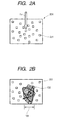
- FIGS. 2A and 2B are drawings for describing a photochemical reaction of a conventional chemically amplified resist.
- FIG. 3 illustrates dependence of the speed of dissolution of the photosensitive compound into a developer solution on the ratio of nitrobenzyl ether introduction in the photosensitive compound.
- FIG. 4 illustrates extinction coefficients of coating films of photosensitive compounds A to D and PHS (polyhydroxystyrene) in Example 4 of the present invention.
- FIG. 5A is an atomic force photomicrograph of a resist pattern having a pitch of 90 nm employing photosensitive composition M.
- FIG. 5B is an atomic force photomicrograph of a resist pattern having a pitch of 90 nm employing photosensitive composition A.
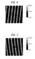
- FIG. 6 is an atomic force photomicrograph of 1 ⁇ m 2 of a resist pattern having a film thickness of 30 nm and a pitch of 160 nm employing photosensitive composition M.
- FIG. 7 is an atomic force photomicrograph of 1 ⁇ m 2 of a resist pattern having a film thickness of 20 nm and a pitch of 160 nm employing photosensitive composition M.
- FIG. 8 is an atomic force photomicrograph of 1 ⁇ m 2 of a resist pattern having a film thickness of 10 nm and a pitch of 160 nm employing photosensitive composition M.
- FIG. 9 is an atomic force photomicrograph of 1 ⁇ m 2 of a resist pattern having a film thickness of 20 nm and a pitch of 160 nm employing photosensitive composition A.
- FIG. 10 is an atomic force photomicrograph of 1 ⁇ m 2 of a resist pattern having a film thickness of 10 nm and a pitch of 160 nm employing photosensitive composition A.
- the present invention provides a photosensitive compound for formation of a resist pattern having a low LER (line edge roughness) even with a small film thickness, a photosensitive composition containing the photosensitive compound, a method of formation of a resist pattern, and a process for producing a device.
- the LER is defined to be three times the standard deviation (3 ⁇ ) of the line pattern breadth.
- line breadths are measured at 50 or more points sampled in a line pattern of 0.5 to 2 ⁇ m long at constant intervals of 10 nm along line length.
- the LER is calculated from the measured line breadths as the population.
- the breadth is measured by scanning electron microscopy, atomic force microscopy, or the like.
- the photosensitive compound of the present invention containing two or more structure units represented by aforementioned General Formula (1) or (6) can be synthesized through a known condensation reaction of a nitrobenzyl alcohol derivative represented by Formula (21) or (22) below with a compound containing two or more phenolic hydroxyl groups in the molecule (hereinafter referred to as "a polyphenolic compound").
- R 1 to R 6 are as defined before, and X is a hydroxyl group or a halogen atom.
- R 1 to R 6 are as defined before, and Y is a hydroxyl or a halogen atom.
- the polyphenolic compounds used in the above condensation reaction are roughly classified into polymer compounds, compounds having a molecular weight of not higher than 2000, and low-molecular compounds constituted of one or more monomers.
- the polyphenolic compound is preferably a low-molecular compound, or a polymer compound having a weight-average molecular weight (Mw) ranging from 1000 to 100000, more preferably from 3000 to 50000 and having molecular weight distribution (Mw/Mn) ranging from 1.0 to 3.0, preferably from 1.0 to 1.5, more preferably from 1.0 to 1.2.
- Mw weight-average molecular weight
- Mw/Mn molecular weight distribution
- the narrower molecular weight distribution gives smaller LER (line edge roughness).
- Particularly preferred are hydroxystyrene homopolymers having a weight-average molecular weight ranging from 3000 to 50000 and a molecular weight distribution ranging from 1.0 to 1.2.
- the phenol group or groups are nitrobenzyl-etherified or nitrobenzyl-carbonated to give the unit structure represented by General Formula (1) or (6).
- not all of the phenol groups in the polyphenolic compound may be nitrobenzyl-etherified or nitrobenzyl-carbonated.
- Two or more of the phenol groups in the molecule are preferably nitrobenzyl-etherified or nitrobenzyl-carbonated, and the nitrobenzyl-etherification degree or the nitrobenzyl-carbonation degree is preferably in the range from 10% to 90%, more preferably from 10% to 50%.
- a higher degree of the nitrobenzyl-etherification or nitrobenzyl-carbonation than 90% necessitates a larger quantity of exposure light for the resist pattern formation, and lowers the adhesiveness of the resist onto the worked substrate owing to the lowered polarity.
- a lower degree of the nitrobenzyl-etherification than 10% lowers resistance of the resist pattern against the developer solution.
- the condensation reaction can be allowed to proceed through a known process such as a method described in J. Org. Chem. 68, 9100 (2003 ) or a method described in J. Am. Chem. Soc, 110, 301, (1988 ).
- the compound represented by Formula (21) includes specifically compounds below: 2-nitrobenzyl alcohol, 2-nitrobenzyl chloride, 2-nitrobenzyl bromide, 2-methyl-2-nitrobenzyl alcohol, 2-methyl-2-nitrobenzyl chloride, 2-methyl-2-nitrobenzyl bromide, 3-methyl-2-nitrobenzyl alcohol, 3-methyl-2-nitrobenzyl chloride, 3-methyl-2-nitrobenzyl bromide, 5-methyl-2-nitrobenzyl alcohol, 5-methyl-2-nitrobenzyl chloride, 5-methyl-2-nitrobenzyl bromide, 3-chloro-2-nitrobenzyl alcohol, 3-chloro-2-nitrobenzyl chloride, 3-chloro-2-nitrobenzyl bromide, 4-chloro-2-nitrobenzyl alcohol, 4-chloro-2-nitrobenzyl chloride, 4-chloro-2-nitrobenzyl bromide, 5-chloro-2-nitrobenzyl alcohol, 5-chloro-2-nitrobenzyl chloride, 5-chloro-2-nitrobenzyl bromide, 4,5
- the compound represented by Formula (22) includes specifically compounds below: 2-nitrobenzyl formate, 2-nitrobenzyl chloroformate, 2-nitrobenzyl bromoformate, 2-methyl-2-nitrobenzyl formate, 2-methyl-2-nitrobenzyl chloroformate, 2-methyl-2-nitrobenzyl bromoformate, 3-methyl-2-nitrobenzyl formate, 3-methyl-2-nitrobenzyl chloroformate, 3-methyl-2-nitrobenzyl bromoformate, 5-methyl-2-nitrobenzyl formate, 5-methyl-2-nitrobenzyl chloroformate, 5-methyl-2-nitrobenzyl bromoformate, 3-chloro-2-nitrobenzyl formate, 3-chloro-2-nitrobenzyl chloroformate, 3-chloro-2-nitrobenzyl bromoformate, 4-chloro-2-nitrobenzyl formate, 4-chloro-2-nitrobenzyl chloroformate, 4-chloro-2-nitrobenzyl bromoformate, 5-chloro-2-nitrobenzyl format
- the high-molecular polyphenolic compound is exemplified by condensation reaction products of a phenol and an aldehyde, condensation products of a phenol and a ketone, vinylphenol type polymers such as poly(hydroxystyrens), and isopropenylphenol type polymers.
- the ketone includes acetone, methyl ethyl ketone, diethyl ketone, and diphenyl ketone.
- the phenol includes a monohydric phenols such as phenol, cresol, xylenol, ethylphenol, propylphenol, butylphenol, and phenylphenol; polyhydric phenols such as resorcinol, pyrocatecol, hydroquinone, bisphenol-A, and pyrogallol.
- monohydric phenols such as phenol, cresol, xylenol, ethylphenol, propylphenol, butylphenol, and phenylphenol
- polyhydric phenols such as resorcinol, pyrocatecol, hydroquinone, bisphenol-A, and pyrogallol.
- the aldehyde includes formaldehyde, acetaldehyde, benzaldehyde, and terephthalaldehyde.
- the ketone includes acetone, methyl ethyl ketone, diethyl ketone, and diphenyl ketone.
- the condensation reaction of the phenol with the aldehyde can be conducted by a conventional method.
- the condensation reaction product of the phenol and the aldehyde is exemplified by phenol-novolak resins, cresol-novolak resins, and calixarenes.
- phenol-novolak resins cresol-novolak resins
- calixarenes Through a condensation reaction by use of such a novolak resin or a calixarene as the high-molecular polyphenolic compound, the hydrogen atoms of two or more of the phenolic hydroxyl groups thereof are substituted by the substituent represented by the above Formula (11) or (12) to form a novolak resin or a calixarene of the present invention.
- the vinylphenol type polymer is selected from homopolymers of vinylphenol (hydroxystyrene) and copolymers thereof with a copolymerizable component.
- the copolymerizable component includes acrylic acid, methacrylic acid, styrene, maleic anhydride, maleimide, vinyl acetate, and acrylonitrile; and derivatives thereof.
- the isopropenylphenol type polymer is selected from homopolymers of isopropenylphenol and copolymers thereof with a copolymerizable component.
- the copolymerizable component includes acrylic acid, methacrylic acid, styrene, maleic anhydride, maleimide, vinyl acetate, and acrylonitrile; and derivatives thereof.
- the low molecular polyphenolic compound includes calixarene derivatives and compounds represented by Formulas (31) to (36) below: where R 31 is an alkyl group of 1-4 carbon atoms, a phenyl group, or a 1-naphtyl group; a plurality of R 31 may be the same or different; p is an integer of 1 or more, q is 0 or an integer, and p+q ⁇ 6.
- Z is a single bond, -S-, -O-, -CO-, -COO-, -SO-, -SO 2 -, or -C(R 32 ) 2 - (where R 32 is a hydrogen atom, an alkyl group of 1-6 carbon atoms, an acyl group of 2-11 carbon atoms, a phenyl group, or a naphthyl group, and plural R 32 may be the same or different from each other), or the group represented by Formula (33) below: (where R 31 is the same as in Formula (31) ; t is an integer of 0-4.
- R 31 is the same as in Formula (31), and R 32 is the same as in Formula (32); p, q, r, s, u, and v are respectively an integer of 0 or more; and p+q ⁇ 5, r+s ⁇ 5, u+v ⁇ 5, and p+r+u ⁇ 1.
- R 31 is the same as in Formula (31); R 32 and Z are the same as in Formula (32); plural R 31 are the same or different from each other; plural R 32 are the same or different from each other; p, q, r, s, u, v, w, and x are respectively an integer of 0 or more; and p+q ⁇ 5, r+s ⁇ 5, u+v ⁇ 5, w+x ⁇ 5, and p+r+u+w ⁇ 1.
- R 31 is the same as in Formula (31); R 32 is the same as in Formula (32); plural R 31 are the same or different from each other; plural R 32 are the same or different from each other; p, q, r, s, u, v, w, and x are respectively an integer of 0 or more; and p+q ⁇ 5, r+s ⁇ 5, u+v ⁇ 5, w+x ⁇ 4, and p+r+u+w ⁇ 1.
- the photosensitive compound of the present invention produces a phenolic hydroxyl group, an alkali-solubilizing group, directly through a photochemical reaction as shown in Reaction Formula (1) or (2).
- the photosensitive compound functions as a positive resist: a light-exposed portion thereof is dissolved by a developer solution.
- Reaction Formula (1) shows the process of the photochemical reaction of nitrobenzyl phenyl ether
- Reaction Formula (2) shows the process of the photochemical reaction of nitrobenzyl phenyl carbonate.
- the photosensitive compound of the present invention may be dissolved in a solvent at a solid concentration ranging from 2% to 50% by weight for use as a photosensitive composition.
- the photosensitive composition is preferably filtered through a filter of pore diameter of about 0.1 to 0.2 ⁇ m.
- the above-mentioned solvent is not limited specially and can be selected arbitrarily, insofar as the solvent is capable of dissolving the photosensitive compound and will not react with the photosensitive compound.
- the solvent may be a simple solvent, or a mixture of solvents.
- the solvent includes ethers, esters, ether esters, ketones, ketone esters, amides, amide esters, lactams, lactones, hydrocarbons, and halogenated hydrocarbons.
- the solvent includes ethylene glycol monoalkyl ethers, diethylene glycol dialkyl ethers, ethylene glycol monoalkyl ether acetates, propylene glycol monoalkyl ether acetates, propylene glycol monoalkyl ethers, propylene glycol dialkyl ethers, acetate esters, hydroxyacetate esters, lactate esters, alkoxyacetate esters, cyclic or acyclic ketones, acetoacetate esters, pyruvate esters, propionate esters, N,N-dialkylformamides, N,N-dialkylacetamides, N-alkylpyrrolidones, ⁇ -lactones, (halogenated) aliphatic hydrocarbons, and (halogenated) aromatic hydrocarbons.
- examples of the solvents are as follows: ethylene glycol monomethyl ether, ethylene glycol monoethyl ether, ethylene glycol mono-n-propyl ether, ethylene glycol mono-n-butyl ether, diethylene glycol dimethyl ether, diethylene glycol diethyl ether, diethylene glycol di-n-propyl ether, diethylene glycol di-n-butyl ether, ethylene glycol monomethyl ether acetate, ethylene glycol monoethyl ether acetate, ethylene glycol mono-n-propyl ether acetate, propylene glycol monomethyl ether acetate (PGMEA), propylene glycol monoethyl ether acetate, propylene glycol mono-n-propyl ether acetate, isopropenyl acetate, isopropenyl propionate, toluene, xylene, methyl ethyl ketone, cyclohexanone,
- propylene glycol monomethyl ether acetate PGMEA
- ethyl-2-hydroxypropionate ethyl-2-hydroxypropionate
- cyclohexanone ethyl-2-hydroxypropionate
- the above-mentioned solvent may contain one or more high-boiling solvents as necessary.
- the high-boiling solvent includes benzyl ethyl ether, di-n-hexyl ether, diethylene glycol monomethyl ether, diethylene glycol monoethyl ether, acetonylacetone, isophorone, caproic acid, caprylic acid, 1-octanol, 1-nonanol, benzyl alcohol, benzyl acetate, ethyl benzoate, diethyl oxalate, diethyl maleate, ⁇ -butyrolactone, ethylene carbonate, propylene carbonate, and ethylene glycol monophenyl ether acetate.
- the photosensitive composition of the present invention may contain a surfactant at a content of not more than 0.2 part by weight based on the total weight (100 parts) of the photosensitive compound, preferably ranging from 0.001 to 0.05 part, more preferably from 0.003 to 0.02 part by weight.
- the surfactant includes fluorine type surfactants; silicone type surfactants; polyoxyethylene alkyl ethers such as polyoxyethylene lauryl ether, polyoxyethylene stearyl ether, and polyoxyethylene oleyl ether; polyoxyethylene aryl ethers such as polyoxyethylene octyl phenyl ether, and polyoxyethylene nonyl phenyl ether; polyoxyethylene dialkyl esters such as polyoxyethylene dilaurate, and polyoxyethylene distearate.
- fluorine type surfactants such as polyoxyethylene lauryl ether, polyoxyethylene stearyl ether, and polyoxyethylene oleyl ether
- polyoxyethylene aryl ethers such as polyoxyethylene octyl phenyl ether, and polyoxyethylene nonyl phenyl ether
- polyoxyethylene dialkyl esters such as polyoxyethylene dilaurate, and polyoxyethylene distearate.
- surfactants include BM-1000, and BM-1100 (BM Chemie Co.); Megafack F142D, F144D, F171, F172, F 173, F177, F178A, F178K, F179, F183, F184, and F191 (Dainippon Ink & Chemicals Inc.); Florard FC-135, FC-170C, FC-171, FC-176, FC-430, and FC-431; Megafack RS-1, RS-7, RS-9, RS-15, and R-08 (Sumitomo 3M Ltd.); Surflon S-112, S-113, S-131, S-141, S-145, S-382, SC-101, SC-102, SC-103, SC-104, SC-105, and SC-106 (Asahi Glass Co.); F-Top EF301, EF303, and EF 352 (Shin Akita Kasei K.K.); SH-28PA, SH-190, SH-193, SZ-6032, SF-84
- the photosensitive composition may contain further a known additive such as a colorant, an auxiliary adhesive, a storage stabilizer, and a defoaming agent.
- a solution of the photosensitive composition of the present invention can be applied by a known application apparatus such as a spin coater, a dip coater, and a roller coater by a known method.
- the applied film has usually a thickness ranging from 0.01 to 5 ⁇ m after prebaking, depending on the use thereof.
- the material of the substrate for the photosensitive composition includes metals, semiconductors, glass, quartz, BN, and organic materials.
- the substrate may be coated with a film or films of a resist, a spin-on-glass material, an organic substance, a metal, an oxide, a nitride, or the like.
- the substrate coated with plural kinds of coating films is exemplified by a substrate coated with a lamination of a resist layer susceptible to plasma etching and another resist layer resistant to plasma etching.
- a preferred example is a substrate which is coated with an underlayer of a resist susceptible to oxygen dry-etching and a layer resistant to oxygen plasma etching formed in the named order.
- the resist for the underlayer includes thermosetting phenol resins, but is not limited thereto.
- the oxygen-plasma-resistant layer may be formed from SiO 2 , TiO 2 , or a spin-on-glass material, but is not limited thereto.
- the resist underlayer is formed in a thickness ranging preferably from 0.01 to 1 ⁇ m.
- the layer resistant to oxygen plasma etching is formed in a thickness ranging preferably from 0.001 to 1 ⁇ m.
- the applied coating film of the photosensitive composition is prebaked suitably, depending on the boiling point of the solvent or other properties of the photosensitive composition, at a temperature ranging from 50°C to 150°C, preferably from 80°C to 110°C.
- the prebaking can be conducted by a hot-plate, a hot-air drier, or a like heating means.
- the applied photosensitive composition layer is exposed to imagewise irradiation selectively through a mask by a known exposure system.
- the irradiation ray for the exposure includes visible rays, ultraviolet rays, far ultraviolet rays, X-rays, electron rays, ⁇ -rays, molecular beams, and ion beams.
- the ray is selected suitably.
- irradiation rays may be employed.
- the exposure may be conducted by near-field light which is generated by a photomask having a light absorber having an aperture breadth smaller than the wavelength of exposure light source.
- the above-mentioned irradiation rays are useful.
- the irradiation may be conducted with a single beam or two or more kinds of beams in combination.
- the near-field exposure is conducted by bringing the light absorber close to the irradiation object so that the near-field light may reach the irradiation object (for instance, close contact with the object).
- shorter wavelength beams such as ArF excimer laser beams, F2 excimer laser beams, EUV beams, electron beams, and near-field light which is not affected by diffraction limit.
- photoreaction spot 103 the region in which one photon can induce a deprotection reaction is defined as photoreaction spot 103.
- one photon h ⁇ introduced into resist layer 204 produces one molecule of an acid: the acid as a catalyst diffuses by promotion by the heat given before the development to induce deprotection reaction of plural alkali-solubilizing groups 201 protected by an acid-decomposable protecting group to give plural alkali-solubilizing groups 102. Therefore, one photoreaction spot in the chemically amplified resist has a size of about 10 nm.
- the heat treatment before the development is not necessary, so that one photon induces deprotection of one group in a molecule of the photosensitive compound of the present invention.
- one photon h ⁇ introduced into the resist layer produces one free alkali-solubilizing group 102 from one alkali-solubilizing group 101 protected by a photo-decomposable protecting group. Therefore, the photoreaction spot in the present invention has a size of a molecular scale (ranging from 0.1 to 1 nm). This enables decrease of LER of a resist pattern.
- the exposed portion (irradiated portion) of the photosensitive resist layer is developed and removed, and the resist is washed and dried to obtain an intended resist pattern.
- an aqueous alkaline solution containing the compound exemplified below is used as the developer solution: sodium hydroxide, potassium hydroxide, sodium carbonate, sodium silicate, sodium metasilicate, ammonia, ethylamine, n-propylamine, diethylamine, di-n-propylamine, triethylamine, methyldiethylamine, dimethylethanolamine, triethanolamine, tetramethylammonium hydroxide, tetraethylammonium hydroxide, pyrrole, piperidine, choline, 1,8-diazabicyclo[5.4.0]-7-undecene, and 1,5-diazabicyclo[4.3.0]-5-nonene.
- the developer solution may contain a water-soluble organic solvent such as methanol, and ethanol, or a surfactant in a suitable amount.
- An aqueous 2.38-wt% tetramethylammonium hydroxide solution is particularly preferred
- the development is conducted by dipping, spraying, brushing, slapping, or a like method.
- the oxygen plasma-resistant layer is etched through the above-mentioned resist pattern as the mask.
- the etching may be conducted either by wet etching or by dry etching.
- the dry etching is suitable for fine pattern formation and is preferred.
- the etchant for the wet etching is selected depending on the etching object, including aqueous fluoric acid solutions, aqueous ammonium fluoride solutions, aqueous phosphoric acid solutions, aqueous acetic acid solutions, aqueous nitric acid solutions, and aqueous cerium ammonium nitrate solutions.
- the gas for dry etching includes CHF 3 , CF 4 , C 2 F 6 , SF 6 , CCl 4 , BCl 3 , Cl 2 , HCl, H 2 , and Ar, and mixtures thereof.
- oxygen plasma etching is conducted through the patterned oxygen plasma-resistant layer as the mask.
- the oxygen-containing gas for the oxygen plasma etching includes simple oxygen, mixtures of oxygen with an inert gas such as argon, mixtures of oxygen with carbon monoxide, carbon dioxide, ammonia, dinitrogen monoxide, or sulfur dioxide.
- a resist pattern can be obtained which has a higher aspect ratio than the resist pattern formed by exposure and development.
- a substrate such as a semiconductor substrate of silicon, germanium, or the like is dry-etched or wetetched.
- the substrate is further worked by metal vapor deposition, lift-off, plating, and so forth to form an intended device on the substrate.
- a semiconductor device can be prepared as described below.
- a device circuit of a semiconductor is designed.
- a mask is prepared which has a circuit pattern corresponding to the intended circuit.
- a substrate for the device is prepared, and thereon the photosensitive composition of the present invention is laminated.
- the circuit is formed on the substrate by lithography with the mask and a conventional exposure system.
- the process for formation of the circuit includes oxide film formation, etching, insulation film formation, conductive wiring film formation, and patterning.
- the substrate having the circuit is subjected to an assembly process (dicing, and bonding), packaging, and so forth, and is chipped.
- PHS poly(hydroxystyrene)
- Mw weight-average molecular weight
- Mw/Mn molecular weight distribution
- the viscous polymer was dissolved in 80 mL of ethyl acetate. The solution was added slowly dropwise into 1.2 L of hexane. The reprecipitated crystal was washed with hexane, and dried under a high vacuum to obtain pale yellow solid of photosensitive compound A (nitrobenzyl ether group introduction degree: 38%).
- Reaction Formula (3) shows the pathway of the synthesis of photosensitive compound A: where m and n are both an integer of 0 or more.
- Photosensitive Compound A Through the same synthetic pathway as above of Photosensitive Compound A, synthesis was conducted by changing the amounts of addition of sodium hydride and 4,5-dimethoxy-2-nitrobenzyl bromide to obtain photosensitive compounds. As the results, were obtained Photosensitive Compound B (nitrobenzyl ether group introduction degree: 26%), Photosensitive Compound C (nitrobenzyl ether group introduction degree: 20%), and Photosensitive Compound D (nitrobenzyl ether group introduction degree: 16%).
- the Photosensitive Compounds A to D were dissolved respectively in propylene glycol monomethyl ether acetate (PGMEA) at a concentration of 10 wt% to obtain Photosensitive Compositions A' to D'.
- PGMEA propylene glycol monomethyl ether acetate
- Photosensitive Compounds A to D were dissolved respectively in PGMEA at a concentration of 1.25 wt% to obtain Photosensitive Compositions A" to D".
- Photosensitive compounds A' to D' and a 10-wt% PHS solution in PGMEA PHS having a weight-average molecular weight (Mw) or 4100 and a molecular weight distribution (Mw/Mn) of 1.1
- PHS weight-average molecular weight
- Mw/Mn molecular weight distribution
- the substrates coated with the compositions were heated on a hot plate at 90°C for 90 seconds to obtain five coating films of Photosensitive Compounds A-D and polyhydroxystyrene (PHS) formed on the substrates.
- PHS polyhydroxystyrene
- the five substrates were immersed in an aqueous 2.38-wt% tetramethylammonium hydroxide solution.
- the film thicknesses were measured before and after the immersion by spectroscopic ellilpsometer to estimate the speed of dissolution (nm/s) into the developer solution.
- FIG. 3 shows dependence of the dissolution speed into the developer solution on nitrobenzyl ether introduction degree of the photosensitive compound.
- Photosensitive Compound A (nitrobenzyl ether introduction degree: 38%) dissolved at a dissolution speed of less than 0.001 nm/s, the speed being outside FIG. 3.
- the speed of development of the unexposed portion of a positive resist is preferably not more than 0.1 nm/s. Therefore, Photosensitive Compositions A and B (nitrobenzyl ether introduction degree: 38%, 26%, respectively) were found to be useful as the positive resist.
- the change of the film thickness of Photosensitive Compound A in the developer immersion test was less than the measurement limit of the spectroscopic ellilpsometer, which prevents measurement of the development velocity.
- FIG. 4 shows extinction coefficients of the coating films of Photosensitive Compounds A-D and PHS in the wavelength range from 200 nm to 500 nm. Photosensitive Compounds A-D were found to absorb light at the wavelength range below 420 nm.
- thermosetting phenol resin AR2455, Rohm & Haas Co.
- spin-on-glass material T-03AS, Honeywell Co.
- HMDS hexamethyldisilazane
- Photosensitive Composition M for comparison was prepared as described below. To 100 weight parts of a chemically amplified positive resist (TDUR-P308EM, Tokyo Ohka Co.) for KrF excimer laser exposure, composed of a poly(hydroxystyrene), was added 5 parts by weight of a photo acid generator (PAG) (CGI1397, Ciba Specialty Chemicals Co.). The mixture was diluted with propylene glycol monomethyl ether acetate (PGMEA) to prepare Photosensitive Composition M.
- PAG photo acid generator
- PEG propylene glycol monomethyl ether acetate
- Photosensitive Composition A or Photosensitive Composition M was respectively applied by spin coating in a thickness after heating of 20 nm, and were heated on a hot plate at 90°C for 90 seconds to prepare resist-coated substrates.
- a photomask for near-field light exposure was prepared which is constituted of a patterned amorphous Si film of 50 nm thick as a light absorber and a supporting silicon nitride film (transparent substrate) of 400 nm thick, the patterned amorphous Si film having a line-and-space pattern of a pitch of 90 nm and a space breadth of about 30 nm.
- This photomask had a membrane structure: the light absorber and the silicon nitride film can be deformed elastically to be close to (e.g., to be contact with) a resist-coated substrate.
- the photomask was placed in opposition to the resist-coated substrate to place the light absorber parallel to the substrate with a gap of 50 ⁇ m.
- the photomask was brought into immediate contact with the resist-coated substrate by deforming the membrane by applying a pressure from the transparent substrate side.
- i-line light (wavelength: 365 nm, illuminance: 250 mW/cm 2 ) of an ultrahigh pressure mercury lamp was projected through an i-line band pass filter from the transparent substrate side. Since the opening space breadth is about 30 nm and is narrower than the wavelength of the projected light, propagation light is intercepted and only the near-field light (wavelength 365 nm) is introduced in the resist film kept in immediate contact with the light absorber.
- the resist-coated substrate coated with Photosensitive Composition A" was immersed into an aqueous 2.38-wt% tetramethylammonium hydroxide solution for 10 seconds, and was rinsed with distilled water for 20 seconds to form a resist pattern of a pitch of 90 nm.
- the resist-coated substrate coated with Photosensitive Composition M after the near-field exposure, was heated on a hot plate at 110°C for 90 seconds, and was immersed and rinsed in the same manner as above.
- FIGS. 5A and 5B are atomic force photomicrographs (AFM) of the resist patterns of the highest resolution on the respective substrates.
- FIG. 5A is an atomic force photomicrograph of a resist pattern of a 90 nm pitch of Photosensitive Composition M.
- FIG. 5B is an atomic force photomicrograph of a resist pattern of a 90 nm pitch of Photosensitive Composition A".
- Photosensitive Composition A enables formation of a resist pattern with sufficiently small LER in comparison with Photosensitive Composition M.
- Two resist-coated substrates coated with Photosensitive Composition A" in a film thickness of 20 nm or 10 nm, and three resist-coated substrates coated with Photosensitive Composition M in a film thickness of 30 nm, 20 nm, or 10 nm were prepared in the same manner as in Example 5.
- a photomask was employed which was the same as the one of Example 5 except that the pattern on the amorphous light absorber had a pitch of 160 nm, and a space breadth of about 60 nm.
- the resist-coated substrates were subjected to heating and development to form resist patterns of a 160 nm pitch.
- FIGS. 6 to 10 are atomic force photomicrographs of the resist patterns having the highest resolution of the respective patterns.
- Photosensitive Compound M tended to give a larger LER at a smaller film thickness range from 30 to 10 nm.
- Photosensitive Compound A" gave a resist pattern of a small LER even with the film thickness of 10 nm.
- Photosensitive Composition M gave a large LER at a film thickness of 10 nm probably because the dilution with PGMEA of Photosensitive Composition M composed of multiple components for a smaller film thickness caused deviation of the composition ratio in application onto the substrate.
- the chemically amplified resist is generally known to cause abnormality of the pattern owing to neutralization of the acid generated at the exposed portion, on the surface, by a basic component existing in the environmental atmosphere. This effect could become remarkable in the film thickness of 10 nm or less.
- the present invention provides a process for forming a resist pattern by employing a photosensitive composition capable of forming a resist pattern with a small LER, and provides also a process for producing a device employing the resist pattern.
- a process for forming a resist pattern comprises the steps of applying on a substrate to form a photosensitive resist layer a photosensitive composition comprising at least one photosensitive compound having, in the molecule, two or more structural units represented by C 6 R 2-6 -CHR 1 -OR 7 or C 6 R 2-6 -CHR 1 -COOR 7 where R 1 is a hydrogen atom or an alkyl group, at least one of R 2 , R 3 , R 4 , R 5 , and R 6 is a nitro group, and others are selected from the group consisting of a hydrogen atom, a halogen atom, an alkyl, an alkoxy, a phenyl, a naphthyl, and an alkyl in which a part or the entire of
Landscapes
- Physics & Mathematics (AREA)
- General Physics & Mathematics (AREA)
- Chemical & Material Sciences (AREA)
- Organic Chemistry (AREA)
- Spectroscopy & Molecular Physics (AREA)
- Ceramic Engineering (AREA)
- Engineering & Computer Science (AREA)
- Materials For Photolithography (AREA)
- Organic Low-Molecular-Weight Compounds And Preparation Thereof (AREA)
- Phenolic Resins Or Amino Resins (AREA)
- Addition Polymer Or Copolymer, Post-Treatments, Or Chemical Modifications (AREA)
- Exposure And Positioning Against Photoresist Photosensitive Materials (AREA)
- Photosensitive Polymer And Photoresist Processing (AREA)
Abstract
Description
- The present invention relates to a photosensitive compound, a photosensitive composition containing the photosensitive compound dissolved in a solvent, a method for resist pattern formation by use of the photosensitive composition, and a process for producing a device by the method for the resist pattern formation.
- In recent years, for fine working in semiconductor and other electronic device industries, higher density and higher integration in the devices are required. In the semiconductor device production process, photolithography is an important technique in fine pattern formation.
- The photolithography employs essentially a technique for stable fine working to a precision of 100 nm or finer. Therefore, the resist used in the photolithography should enable formation of a pattern to a precision of 100 nm or finer.
- Diazonaphtoquinone-novolak type resists are widely used which utilize a dissolution inhibition effect of the diazonaphthoquinone compound on a phenol resin (
USP 4, 859, 563 ) . - A diazonaphthoquinone-novolak type resist constituted of a low-molecular phenol resin cannot be affected by the dissolution inhibition effect of the naphthoquinone compound, resulting in a low development contrast between exposed regions and unexposed regions.
- Lately, chemically amplified resists are used as a high-resolution resist rather than the diazonaphthoquinone-novolak type resist. In the chemically amplified resist, an acid (H+) is generated by irradiation with an active ray, and the generated acid catalyzes the deprotection reaction of an alkali-solubilizing group protected by an acid-decomposable protecting group to make the resist soluble in alkali (Journal of Photopolymer Science and Technology 17, 435, (2004)).
- In formation of a resist pattern of a chemically amplified resist, the resist is heat-treated prior to the development in order to accelerate the deprotection reaction catalyzed by the acid generated in the exposed region.
- In this heat treatment, the acid is allowed to diffuse to a distance of about 10 nm by the heat ("Proc. SPIE", 6154, 710, 2006). This diffusion of the acid causes fine roughness at the edge portions of the pattern, namely line edge roughness (LER), to lower the resolution.
- The LER depends also on the molecular weight of the base compound. The base compound herein denotes a compound having an alkali-solubilizing group or a protected alkali-solubilizing group in the resist composition.
- Since the base compound dissolves, molecule by molecule, into the developing solution, a larger molecular weight of the base compound causes larger LER.
- A base compound of a lower molecular weight has a lower glass transition temperature and a lower melting point. When the chemically amplified resist is heated before the development treatment at a temperature higher than its glass transition temperature, the formed acid diffuses to a longer distance to lower the resolution.
- Therefore, the base compound of the chemically amplified resist should have a glass transition temperature higher than the deprotection reaction temperature under acid catalysis. This requirement limits the design of the chemically amplified resist for a lower LER (line edge roughness) by use of a lower molecular-weight resist.
- The inventors of the present invention found that, in a pattern formation by near-field light exposure, when a chemically amplified resist diluted with an organic solvent is applied in a thickness of 10 nm, the LER of the resulting resist pattern is larger undesirably.
- J. Org. Chem. 2003, 68, 9100 (2003) discloses a caged compound having a latent physiological activity formed by nitrobenzyl-etherifying the phenolic hydroxyl group of capsaicin. This compound is not intended for use as a pattern-forming material.
- J. Appl. Polym. Sci., 33, 1763 (1987) discloses a photosensitive polyimide resist having a nitrobenzyl group. This resist can be made alkali-soluble by light irradiation to eliminate the nitrobenzyl from the polyimide. The polymer of this resist is solubilized by elimination of the nitrobenzyl to form a carboxylic acid group (COOH). However, this resist gives resolution of as low as a micrometer order owing to swelling of the resist polymer caused by the reaction of the carboxylic acid with the alkali developing solution.
- The present invention is directed to a photosensitive compound having, in the molecule, two or more structural units represented by General Formula (1) :

- The photosensitive compound can have two or more structural units represented by General Formula (2) in the molecule:

- The photosensitive compound can have two or more structural units represented by General Formula (3) in the molecule:

- The photosensitive compound can have two or more structural units represented by General Formula (4) in the molecule:

- The photosensitive compound can have two or more structural units represented by General Formula (5) in the molecule:

- The present invention is directed to a photosensitive compound having, in the molecule, two or more structural units represented by General Formula (6) :

- The photosensitive compound has two or more structural units represented by General Formula (7) in the molecule:

- The photosensitive compound can have two or more structural units represented by General Formula (8) in the molecule:

- The photosensitive can have two or more structural units represented by General Formula (9) in the molecule:

- The photosensitive compound can have two or more structural units represented by General Formula (10) in the molecule:

- The present invention is directed to a poly(hydroxystyrene) in which hydrogen atoms of two or more hydroxyl groups are substituted by the substituent represented by General Formula (11) or (12):


- The present invention is directed to a calixarene in which hydrogen atoms of two or more phenolic hydroxyl groups are substituted by the substituent represented by General Formula (11) or (12):


- The present invention is directed to a novolak resin in which in which hydrogen atoms of two or more phenolic hydroxyl groups are substituted by the substituent represented by General Formula (11) or (12):


- The present invention is directed to a photosensitive composition comprising at least one of the compounds set forth above dissolved in an organic solvent.
- The present invention is directed to a process for forming a resist pattern comprising the steps of: applying the photosensitive composition set forth above on a substrate to form a photosensitive resist layer, irradiating the resist layer selectively with a radiation ray, and developing a portion irradiated by the ray to form a pattern of the resist layer.
- In the process for forming a resist pattern, a resist layer capable of being removed by plasma etching and another resist layer resistant to plasma etching can be laminated, and the photosensitive resist layer can be formed on the layer resistant to plasma etching.
- In the process for forming a resist pattern, the photosensitive resist layer can be formed in a thickness not more than 20 nm.
- In the process for forming a resist pattern, the irradiation of the radiation ray can be conducted with near-field light.
- The present invention is directed to a process for producing a device, in which the device is formed on a substrate by the process for forming a resist pattern set forth above.
- The photosensitive compound of the present invention need not be heated after the light exposure in resist pattern formation. Therefore, a lower-molecular phenol compound can be used without heating regardless of the restriction in the glass-transition temperature and melting point in the present invention. The photosensitive compound of the present invention enables formation of a resist pattern with a low LER.
- Further features of the present invention will become apparent from the following description of exemplary embodiments with reference to the attached drawings.
- FIG. 1 is a drawing for describing the photochemical reaction of the photosensitive compound of the present invention.
- FIGS. 2A and 2B are drawings for describing a photochemical reaction of a conventional chemically amplified resist.
- FIG. 3 illustrates dependence of the speed of dissolution of the photosensitive compound into a developer solution on the ratio of nitrobenzyl ether introduction in the photosensitive compound.
- FIG. 4 illustrates extinction coefficients of coating films of photosensitive compounds A to D and PHS (polyhydroxystyrene) in Example 4 of the present invention.
- FIG. 5A is an atomic force photomicrograph of a resist pattern having a pitch of 90 nm employing photosensitive composition M.
- FIG. 5B is an atomic force photomicrograph of a resist pattern having a pitch of 90 nm employing photosensitive composition A.
- FIG. 6 is an atomic force photomicrograph of 1 µm2 of a resist pattern having a film thickness of 30 nm and a pitch of 160 nm employing photosensitive composition M.
- FIG. 7 is an atomic force photomicrograph of 1 µm2 of a resist pattern having a film thickness of 20 nm and a pitch of 160 nm employing photosensitive composition M.
- FIG. 8 is an atomic force photomicrograph of 1 µm2 of a resist pattern having a film thickness of 10 nm and a pitch of 160 nm employing photosensitive composition M.
- FIG. 9 is an atomic force photomicrograph of 1 µm2 of a resist pattern having a film thickness of 20 nm and a pitch of 160 nm employing photosensitive composition A.
- FIG. 10 is an atomic force photomicrograph of 1 µm2 of a resist pattern having a film thickness of 10 nm and a pitch of 160 nm employing photosensitive composition A.
- The present invention provides a photosensitive compound for formation of a resist pattern having a low LER (line edge roughness) even with a small film thickness, a photosensitive composition containing the photosensitive compound, a method of formation of a resist pattern, and a process for producing a device.
- In the present invention, the LER is defined to be three times the standard deviation (3σ) of the line pattern breadth. For estimation of the LER, line breadths are measured at 50 or more points sampled in a line pattern of 0.5 to 2 µm long at constant intervals of 10 nm along line length. The LER is calculated from the measured line breadths as the population. The breadth is measured by scanning electron microscopy, atomic force microscopy, or the like.
- The photosensitive compound of the present invention containing two or more structure units represented by aforementioned General Formula (1) or (6) can be synthesized through a known condensation reaction of a nitrobenzyl alcohol derivative represented by Formula (21) or (22) below with a compound containing two or more phenolic hydroxyl groups in the molecule (hereinafter referred to as "a polyphenolic compound").
-

-

- The polyphenolic compounds used in the above condensation reaction are roughly classified into polymer compounds, compounds having a molecular weight of not higher than 2000, and low-molecular compounds constituted of one or more monomers. The polyphenolic compound is preferably a low-molecular compound, or a polymer compound having a weight-average molecular weight (Mw) ranging from 1000 to 100000, more preferably from 3000 to 50000 and having molecular weight distribution (Mw/Mn) ranging from 1.0 to 3.0, preferably from 1.0 to 1.5, more preferably from 1.0 to 1.2. The narrower molecular weight distribution gives smaller LER (line edge roughness). Particularly preferred are hydroxystyrene homopolymers having a weight-average molecular weight ranging from 3000 to 50000 and a molecular weight distribution ranging from 1.0 to 1.2.
- Through the above condensation reaction, the phenol group or groups are nitrobenzyl-etherified or nitrobenzyl-carbonated to give the unit structure represented by General Formula (1) or (6).
- In the above condensation reaction, not all of the phenol groups in the polyphenolic compound may be nitrobenzyl-etherified or nitrobenzyl-carbonated. Two or more of the phenol groups in the molecule are preferably nitrobenzyl-etherified or nitrobenzyl-carbonated, and the nitrobenzyl-etherification degree or the nitrobenzyl-carbonation degree is preferably in the range from 10% to 90%, more preferably from 10% to 50%. A higher degree of the nitrobenzyl-etherification or nitrobenzyl-carbonation than 90% necessitates a larger quantity of exposure light for the resist pattern formation, and lowers the adhesiveness of the resist onto the worked substrate owing to the lowered polarity. A lower degree of the nitrobenzyl-etherification than 10% lowers resistance of the resist pattern against the developer solution.
- The condensation reaction can be allowed to proceed through a known process such as a method described in J. Org. Chem. 68, 9100 (2003) or a method described in J. Am. Chem. Soc, 110, 301, (1988).
- The compound represented by Formula (21) includes specifically compounds below: 2-nitrobenzyl alcohol, 2-nitrobenzyl chloride, 2-nitrobenzyl bromide, 2-methyl-2-nitrobenzyl alcohol, 2-methyl-2-nitrobenzyl chloride, 2-methyl-2-nitrobenzyl bromide, 3-methyl-2-nitrobenzyl alcohol, 3-methyl-2-nitrobenzyl chloride, 3-methyl-2-nitrobenzyl bromide, 5-methyl-2-nitrobenzyl alcohol, 5-methyl-2-nitrobenzyl chloride, 5-methyl-2-nitrobenzyl bromide, 3-chloro-2-nitrobenzyl alcohol, 3-chloro-2-nitrobenzyl chloride, 3-chloro-2-nitrobenzyl bromide, 4-chloro-2-nitrobenzyl alcohol, 4-chloro-2-nitrobenzyl chloride, 4-chloro-2-nitrobenzyl bromide, 5-chloro-2-nitrobenzyl alcohol, 5-chloro-2-nitrobenzyl chloride, 5-chloro-2-nitrobenzyl bromide, 4,5-dimethoxy-2-nitrobenzyl alcohol, 4,5-dimethoxy-2-nitrobenzyl chloride, 4,5-dimethoxy-2-nitrobenzyl bromide, 5-(3-iodopropoxy)-2-nitrobenzyl alcohol, 5-(3-iodopropoxy)-2-nitrobenzyl chloride, and 5-(3-iodopropoxy)-2-nitrobenzyl bromide.
- The compound represented by Formula (22) includes specifically compounds below: 2-nitrobenzyl formate, 2-nitrobenzyl chloroformate, 2-nitrobenzyl bromoformate, 2-methyl-2-nitrobenzyl formate, 2-methyl-2-nitrobenzyl chloroformate, 2-methyl-2-nitrobenzyl bromoformate, 3-methyl-2-nitrobenzyl formate, 3-methyl-2-nitrobenzyl chloroformate, 3-methyl-2-nitrobenzyl bromoformate, 5-methyl-2-nitrobenzyl formate, 5-methyl-2-nitrobenzyl chloroformate, 5-methyl-2-nitrobenzyl bromoformate, 3-chloro-2-nitrobenzyl formate, 3-chloro-2-nitrobenzyl chloroformate, 3-chloro-2-nitrobenzyl bromoformate, 4-chloro-2-nitrobenzyl formate, 4-chloro-2-nitrobenzyl chloroformate, 4-chloro-2-nitrobenzyl bromoformate, 5-chloro-2-nitrobenzyl formate, 5-chloro-2-nitrobenzyl chloroformate, 5-chloro-2-nitrobenzyl bromoformate, 4,5-dimethoxy-2-nitrobenzyl formate, 4,5-dimethoxy-2-nitrobenzyl chloroformate, 4,5-dimethoxy-2-nitrobenzyl bromoformate, 5-(3-iodopropoxy)-2-nitrobenzyl formate, 5-(3-iodopropoxy)-2-nitrobenzyl chloroformate, and 5-(3-iodopropoxy)-2-nitrobenzyl bromoformate.
- The high-molecular polyphenolic compound is exemplified by condensation reaction products of a phenol and an aldehyde, condensation products of a phenol and a ketone, vinylphenol type polymers such as poly(hydroxystyrens), and isopropenylphenol type polymers.
- The ketone includes acetone, methyl ethyl ketone, diethyl ketone, and diphenyl ketone.
- The phenol includes a monohydric phenols such as phenol, cresol, xylenol, ethylphenol, propylphenol, butylphenol, and phenylphenol; polyhydric phenols such as resorcinol, pyrocatecol, hydroquinone, bisphenol-A, and pyrogallol.
- The aldehyde includes formaldehyde, acetaldehyde, benzaldehyde, and terephthalaldehyde.
- The ketone includes acetone, methyl ethyl ketone, diethyl ketone, and diphenyl ketone.
- The condensation reaction of the phenol with the aldehyde can be conducted by a conventional method. The condensation reaction product of the phenol and the aldehyde is exemplified by phenol-novolak resins, cresol-novolak resins, and calixarenes. Through a condensation reaction by use of such a novolak resin or a calixarene as the high-molecular polyphenolic compound, the hydrogen atoms of two or more of the phenolic hydroxyl groups thereof are substituted by the substituent represented by the above Formula (11) or (12) to form a novolak resin or a calixarene of the present invention.
- The vinylphenol type polymer is selected from homopolymers of vinylphenol (hydroxystyrene) and copolymers thereof with a copolymerizable component. The copolymerizable component includes acrylic acid, methacrylic acid, styrene, maleic anhydride, maleimide, vinyl acetate, and acrylonitrile; and derivatives thereof.
- The isopropenylphenol type polymer is selected from homopolymers of isopropenylphenol and copolymers thereof with a copolymerizable component. The copolymerizable component includes acrylic acid, methacrylic acid, styrene, maleic anhydride, maleimide, vinyl acetate, and acrylonitrile; and derivatives thereof.
- The low molecular polyphenolic compound includes calixarene derivatives and compounds represented by Formulas (31) to (36) below:


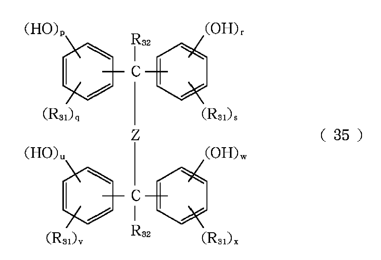

- The photosensitive compound of the present invention produces a phenolic hydroxyl group, an alkali-solubilizing group, directly through a photochemical reaction as shown in Reaction Formula (1) or (2). Thus the photosensitive compound functions as a positive resist: a light-exposed portion thereof is dissolved by a developer solution.
- Reaction Formula (1) shows the process of the photochemical reaction of nitrobenzyl phenyl ether, and Reaction Formula (2) shows the process of the photochemical reaction of nitrobenzyl phenyl carbonate.


- The photosensitive compound of the present invention may be dissolved in a solvent at a solid concentration ranging from 2% to 50% by weight for use as a photosensitive composition. The photosensitive composition is preferably filtered through a filter of pore diameter of about 0.1 to 0.2 µm.
- The above-mentioned solvent is not limited specially and can be selected arbitrarily, insofar as the solvent is capable of dissolving the photosensitive compound and will not react with the photosensitive compound. The solvent may be a simple solvent, or a mixture of solvents. The solvent includes ethers, esters, ether esters, ketones, ketone esters, amides, amide esters, lactams, lactones, hydrocarbons, and halogenated hydrocarbons. More specifically, the solvent includes ethylene glycol monoalkyl ethers, diethylene glycol dialkyl ethers, ethylene glycol monoalkyl ether acetates, propylene glycol monoalkyl ether acetates, propylene glycol monoalkyl ethers, propylene glycol dialkyl ethers, acetate esters, hydroxyacetate esters, lactate esters, alkoxyacetate esters, cyclic or acyclic ketones, acetoacetate esters, pyruvate esters, propionate esters, N,N-dialkylformamides, N,N-dialkylacetamides, N-alkylpyrrolidones, γ-lactones, (halogenated) aliphatic hydrocarbons, and (halogenated) aromatic hydrocarbons.
- Still more specifically, examples of the solvents are as follows: ethylene glycol monomethyl ether, ethylene glycol monoethyl ether, ethylene glycol mono-n-propyl ether, ethylene glycol mono-n-butyl ether, diethylene glycol dimethyl ether, diethylene glycol diethyl ether, diethylene glycol di-n-propyl ether, diethylene glycol di-n-butyl ether, ethylene glycol monomethyl ether acetate, ethylene glycol monoethyl ether acetate, ethylene glycol mono-n-propyl ether acetate, propylene glycol monomethyl ether acetate (PGMEA), propylene glycol monoethyl ether acetate, propylene glycol mono-n-propyl ether acetate, isopropenyl acetate, isopropenyl propionate, toluene, xylene, methyl ethyl ketone, cyclohexanone, 2-heptanone, 3-heptanone, 4-heptanone, ethyl 2-hydroxypropionate, ethyl 2-hydroxy-2-methylpropionate, ethyl ethoxyacetate, ethyl hydroxyacetate, methyl 2-hydroxy-3-methylbutyrate, 3-methoxybutyl acetate, 3-methyl-3-methoxybutyl acetate, 3-methyl-3-methoxybutyl propionate, 3-methyl-3-methoxybutyl butyrate, ethyl acetate, n-propyl acetate, n-butyl acetate, methyl acetoacetate, ethyl acetoacetate, methyl 3-methoxypropionate, ethyl 3-methoxypropionate, methyl 3-ethoxypropionate, ethyl 3-ethoxypropionate, N-methylpyrrolidone, N,N-dimethylformamide, and N,N-dimethylacetamide.
- In consideration of safety, preferred are propylene glycol monomethyl ether acetate (PGMEA), ethyl-2-hydroxypropionate, and cyclohexanone.
- The above-mentioned solvent may contain one or more high-boiling solvents as necessary. The high-boiling solvent includes benzyl ethyl ether, di-n-hexyl ether, diethylene glycol monomethyl ether, diethylene glycol monoethyl ether, acetonylacetone, isophorone, caproic acid, caprylic acid, 1-octanol, 1-nonanol, benzyl alcohol, benzyl acetate, ethyl benzoate, diethyl oxalate, diethyl maleate, γ-butyrolactone, ethylene carbonate, propylene carbonate, and ethylene glycol monophenyl ether acetate.
- The photosensitive composition of the present invention may contain a surfactant at a content of not more than 0.2 part by weight based on the total weight (100 parts) of the photosensitive compound, preferably ranging from 0.001 to 0.05 part, more preferably from 0.003 to 0.02 part by weight.
- The surfactant includes fluorine type surfactants; silicone type surfactants; polyoxyethylene alkyl ethers such as polyoxyethylene lauryl ether, polyoxyethylene stearyl ether, and polyoxyethylene oleyl ether; polyoxyethylene aryl ethers such as polyoxyethylene octyl phenyl ether, and polyoxyethylene nonyl phenyl ether; polyoxyethylene dialkyl esters such as polyoxyethylene dilaurate, and polyoxyethylene distearate.
- Commercially available surfactants include BM-1000, and BM-1100 (BM Chemie Co.); Megafack F142D, F144D, F171, F172, F 173, F177, F178A, F178K, F179, F183, F184, and F191 (Dainippon Ink & Chemicals Inc.); Florard FC-135, FC-170C, FC-171, FC-176, FC-430, and FC-431; Megafack RS-1, RS-7, RS-9, RS-15, and R-08 (Sumitomo 3M Ltd.); Surflon S-112, S-113, S-131, S-141, S-145, S-382, SC-101, SC-102, SC-103, SC-104, SC-105, and SC-106 (Asahi Glass Co.); F-Top EF301, EF303, and EF 352 (Shin Akita Kasei K.K.); SH-28PA, SH-190, SH-193, SZ-6032, SF-8428, DC-57, and DC-190 (Dow Corning Toray Silicone Co.); Organosiloxane Polymer KP341 (Shin-Etsu Chemical Co.); (metha)crylate type copolymers Polyflow No.57, No.95 (Kyoeisha Kagaku K.K.); Ftargent FT-250, FT-251, and FTX-218 (Neosu K.K.).
- The photosensitive composition may contain further a known additive such as a colorant, an auxiliary adhesive, a storage stabilizer, and a defoaming agent.
- A solution of the photosensitive composition of the present invention can be applied by a known application apparatus such as a spin coater, a dip coater, and a roller coater by a known method. The applied film has usually a thickness ranging from 0.01 to 5 µm after prebaking, depending on the use thereof.
- The material of the substrate for the photosensitive composition includes metals, semiconductors, glass, quartz, BN, and organic materials. The substrate may be coated with a film or films of a resist, a spin-on-glass material, an organic substance, a metal, an oxide, a nitride, or the like.
- The substrate coated with plural kinds of coating films is exemplified by a substrate coated with a lamination of a resist layer susceptible to plasma etching and another resist layer resistant to plasma etching. A preferred example is a substrate which is coated with an underlayer of a resist susceptible to oxygen dry-etching and a layer resistant to oxygen plasma etching formed in the named order.
- The resist for the underlayer includes thermosetting phenol resins, but is not limited thereto.
- The oxygen-plasma-resistant layer may be formed from SiO2, TiO2, or a spin-on-glass material, but is not limited thereto.
- The resist underlayer is formed in a thickness ranging preferably from 0.01 to 1 µm. The layer resistant to oxygen plasma etching is formed in a thickness ranging preferably from 0.001 to 1 µm.
- The applied coating film of the photosensitive composition is prebaked suitably, depending on the boiling point of the solvent or other properties of the photosensitive composition, at a temperature ranging from 50°C to 150°C, preferably from 80°C to 110°C. The prebaking can be conducted by a hot-plate, a hot-air drier, or a like heating means.
- For pattern formation, the applied photosensitive composition layer is exposed to imagewise irradiation selectively through a mask by a known exposure system. The irradiation ray for the exposure includes visible rays, ultraviolet rays, far ultraviolet rays, X-rays, electron rays, γ-rays, molecular beams, and ion beams. The ray is selected suitably. Preferred are mercury lamp beams (wavelengths: 436 nm, 365 nm, 254 nm), a KrF excimer laser beam (wavelength: 248 nm), an ArF excimer laser beam (wavelength: 193 nm), a F2 excimer laser beam (wavelength: 157 nm), far ultraviolet beams such as an extreme ultraviolet beam (EUV, wavelength: 13 nm), and electron beams. One or more of irradiation rays may be employed.
- Otherwise, the exposure may be conducted by near-field light which is generated by a photomask having a light absorber having an aperture breadth smaller than the wavelength of exposure light source. For the near-field light exposure, the above-mentioned irradiation rays are useful. The irradiation may be conducted with a single beam or two or more kinds of beams in combination. The near-field exposure is conducted by bringing the light absorber close to the irradiation object so that the near-field light may reach the irradiation object (for instance, close contact with the object).
- For finer resist pattern, particularly preferred for the exposure are shorter wavelength beams such as ArF excimer laser beams, F2 excimer laser beams, EUV beams, electron beams, and near-field light which is not affected by diffraction limit.
- The photochemical reaction of the photosensitive composition of the present invention is different from that of conventional chemically amplified resist as described below. In FIGS. 1 and 2B, the region in which one photon can induce a deprotection reaction is defined as
photoreaction spot 103. In conventional methods, one photon hν introduced into resistlayer 204 produces one molecule of an acid: the acid as a catalyst diffuses by promotion by the heat given before the development to induce deprotection reaction of plural alkali-solubilizinggroups 201 protected by an acid-decomposable protecting group to give plural alkali-solubilizinggroups 102. Therefore, one photoreaction spot in the chemically amplified resist has a size of about 10 nm. On the other hand, in the present invention, the heat treatment before the development is not necessary, so that one photon induces deprotection of one group in a molecule of the photosensitive compound of the present invention. In other words, one photon hν introduced into the resist layer produces one free alkali-solubilizing group 102 from one alkali-solubilizing group 101 protected by a photo-decomposable protecting group. Therefore, the photoreaction spot in the present invention has a size of a molecular scale (ranging from 0.1 to 1 nm). This enables decrease of LER of a resist pattern. - After the exposure, the exposed portion (irradiated portion) of the photosensitive resist layer is developed and removed, and the resist is washed and dried to obtain an intended resist pattern.
- For the development, an aqueous alkaline solution containing the compound exemplified below is used as the developer solution: sodium hydroxide, potassium hydroxide, sodium carbonate, sodium silicate, sodium metasilicate, ammonia, ethylamine, n-propylamine, diethylamine, di-n-propylamine, triethylamine, methyldiethylamine, dimethylethanolamine, triethanolamine, tetramethylammonium hydroxide, tetraethylammonium hydroxide, pyrrole, piperidine, choline, 1,8-diazabicyclo[5.4.0]-7-undecene, and 1,5-diazabicyclo[4.3.0]-5-nonene. The developer solution may contain a water-soluble organic solvent such as methanol, and ethanol, or a surfactant in a suitable amount. An aqueous 2.38-wt% tetramethylammonium hydroxide solution is particularly preferred.
- The development is conducted by dipping, spraying, brushing, slapping, or a like method.
- In the case where the resist pattern film is formed on a substrate having an underlying resist layer and an oxygen plasma-resistant layer formed thereon in this order, firstly the oxygen plasma-resistant layer is etched through the above-mentioned resist pattern as the mask. The etching may be conducted either by wet etching or by dry etching. The dry etching is suitable for fine pattern formation and is preferred. The etchant for the wet etching is selected depending on the etching object, including aqueous fluoric acid solutions, aqueous ammonium fluoride solutions, aqueous phosphoric acid solutions, aqueous acetic acid solutions, aqueous nitric acid solutions, and aqueous cerium ammonium nitrate solutions. The gas for dry etching includes CHF3, CF4, C2F6, SF6, CCl4, BCl3, Cl2, HCl, H2, and Ar, and mixtures thereof.
- Next, oxygen plasma etching is conducted through the patterned oxygen plasma-resistant layer as the mask. The oxygen-containing gas for the oxygen plasma etching includes simple oxygen, mixtures of oxygen with an inert gas such as argon, mixtures of oxygen with carbon monoxide, carbon dioxide, ammonia, dinitrogen monoxide, or sulfur dioxide.
- Through the above two-step etching, a resist pattern can be obtained which has a higher aspect ratio than the resist pattern formed by exposure and development.
- With the resist pattern formed as above as the mask, a substrate such as a semiconductor substrate of silicon, germanium, or the like is dry-etched or wetetched. The substrate is further worked by metal vapor deposition, lift-off, plating, and so forth to form an intended device on the substrate. For instance, a semiconductor device can be prepared as described below.
- Firstly, a device circuit of a semiconductor is designed. Then a mask is prepared which has a circuit pattern corresponding to the intended circuit. Separately, a substrate for the device is prepared, and thereon the photosensitive composition of the present invention is laminated.
- Then, the circuit is formed on the substrate by lithography with the mask and a conventional exposure system. The process for formation of the circuit includes oxide film formation, etching, insulation film formation, conductive wiring film formation, and patterning. Next, the substrate having the circuit is subjected to an assembly process (dicing, and bonding), packaging, and so forth, and is chipped.
- [EXAMPLES]
- The present invention is described specifically by reference to Examples.
- Example 1
- Synthesis of Photosensitive Compounds
- In a 100-mL reactor, 4.0 g of poly(hydroxystyrene) (PHS)(33.3 mmol in terms of hydroxystyrene monomer, defined as 1.0 mol-equivalent) was dissolved in 40 mL of N,N-dimethylformamide. The poly(hydroxystyrene) (PHS) had a weight-average molecular weight (Mw) of 4100, and a molecular weight distribution (Mw/Mn) of 1.1.
- To this solution, was added 0.21 g of sodium hydride (8.75 mmol, 0.265 mol-equivalent) at room temperature (23°C), and the mixture was stirred for 30 minutes, and further at 50°C for two hours.
- To this liquid suspension, was added 2.15 g (7.8 mmol, 0.235 mol-equivalent) of 4,5-dimethoxy-2-nitrobenzyl bromide at one time, and the mixture was stirred at 50°C for one hour.
- To this solution, was added again 0.21 g (8.75 mmol, 0.265 mol-equivalent) of sodium hydride, and the mixture was stirred for one hour.
- Then, to this liquid suspension, was added 2.15 g (7.8 mmol, 0.235 mol-equivalent) of 4,5-dimethoxy-2-nitrobenzyl bromide at one time, and the mixture was stirred at 50°C for two hours.
- The resulting solution was stirred at room temperature without heating for 18 hours.
- To this solution, was added 100 mL of an aqueous 10% ammonium chloride solution. The aqueous phase was extracted with 100 mL of ethyl acetate three times. The organic phase portions were combined, and the combined organic phase was washed with 100 mL of water eight times and 100 mL of saturated sodium chloride solution once. The washed organic phase was dried over anhydrous magnesium sulfate, and was concentrated.
- Toluene was added to this solution to precipitate the intended polymer. The supernatant liquid was removed, and toluene was added again thereto, and the polymer was suspended. After left standing, the supernatant was removed.
- The viscous polymer was dissolved in 80 mL of ethyl acetate. The solution was added slowly dropwise into 1.2 L of hexane. The reprecipitated crystal was washed with hexane, and dried under a high vacuum to obtain pale yellow solid of photosensitive compound A (nitrobenzyl ether group introduction degree: 38%).
- Reaction Formula (3) below shows the pathway of the synthesis of photosensitive compound A:
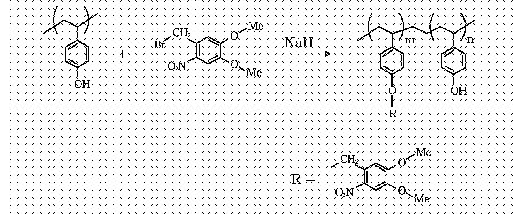
- Through the same synthetic pathway as above of Photosensitive Compound A, synthesis was conducted by changing the amounts of addition of sodium hydride and 4,5-dimethoxy-2-nitrobenzyl bromide to obtain photosensitive compounds. As the results, were obtained Photosensitive Compound B (nitrobenzyl ether group introduction degree: 26%), Photosensitive Compound C (nitrobenzyl ether group introduction degree: 20%), and Photosensitive Compound D (nitrobenzyl ether group introduction degree: 16%).
- Example 2
- Preparation of Photosensitive Compositions
- The Photosensitive Compounds A to D were dissolved respectively in propylene glycol monomethyl ether acetate (PGMEA) at a concentration of 10 wt% to obtain Photosensitive Compositions A' to D'.
- Photosensitive Compounds A to D were dissolved respectively in PGMEA at a concentration of 1.25 wt% to obtain Photosensitive Compositions A" to D".
- Example 3
- Evaluation of Photosensitive Compounds for Resistance to Developer Solution
- Photosensitive compounds A' to D' and a 10-wt% PHS solution in PGMEA (PHS having a weight-average molecular weight (Mw) or 4100 and a molecular weight distribution (Mw/Mn) of 1.1) were respectively applied on Si substrates having been treated with hexamethyldisilazane (HMDS) by spin coating.
- Then the substrates coated with the compositions were heated on a hot plate at 90°C for 90 seconds to obtain five coating films of Photosensitive Compounds A-D and polyhydroxystyrene (PHS) formed on the substrates.
- The five substrates were immersed in an aqueous 2.38-wt% tetramethylammonium hydroxide solution. The film thicknesses were measured before and after the immersion by spectroscopic ellilpsometer to estimate the speed of dissolution (nm/s) into the developer solution.
- FIG. 3 shows dependence of the dissolution speed into the developer solution on nitrobenzyl ether introduction degree of the photosensitive compound. Photosensitive Compound A (nitrobenzyl ether introduction degree: 38%) dissolved at a dissolution speed of less than 0.001 nm/s, the speed being outside FIG. 3.
- Generally, the speed of development of the unexposed portion of a positive resist is preferably not more than 0.1 nm/s. Therefore, Photosensitive Compositions A and B (nitrobenzyl ether introduction degree: 38%, 26%, respectively) were found to be useful as the positive resist.
- The change of the film thickness of Photosensitive Compound A in the developer immersion test was less than the measurement limit of the spectroscopic ellilpsometer, which prevents measurement of the development velocity.
- Example 4
- Measurement of Extinction Coefficient of Photosensitive Compounds
- The extinction coefficients of the coating films, formed in Example 3, of Photosensitive Compounds A-D were measured by spectroscopic ellilpsometer. FIG. 4 shows extinction coefficients of the coating films of Photosensitive Compounds A-D and PHS in the wavelength range from 200 nm to 500 nm. Photosensitive Compounds A-D were found to absorb light at the wavelength range below 420 nm.
- Example 5
- Formation of Resist Pattern by Near-Field Light Exposure (1)
- On a Si substrate, a thermosetting phenol resin (AR2455, Rohm & Haas Co.) of 100 nm thick and a spin-on-glass material (T-03AS, Honeywell Co.) of 20 nm thick were laminated in this order by spin coating.
- The surface of the spin-on-glass material layer was treated with hexamethyldisilazane (HMDS).
- Photosensitive Composition M for comparison was prepared as described below. To 100 weight parts of a chemically amplified positive resist (TDUR-P308EM, Tokyo Ohka Co.) for KrF excimer laser exposure, composed of a poly(hydroxystyrene), was added 5 parts by weight of a photo acid generator (PAG) (CGI1397, Ciba Specialty Chemicals Co.). The mixture was diluted with propylene glycol monomethyl ether acetate (PGMEA) to prepare Photosensitive Composition M.
- On the above-prepared substrate, Photosensitive Composition A" or Photosensitive Composition M was respectively applied by spin coating in a thickness after heating of 20 nm, and were heated on a hot plate at 90°C for 90 seconds to prepare resist-coated substrates.
- A photomask for near-field light exposure was prepared which is constituted of a patterned amorphous Si film of 50 nm thick as a light absorber and a supporting silicon nitride film (transparent substrate) of 400 nm thick, the patterned amorphous Si film having a line-and-space pattern of a pitch of 90 nm and a space breadth of about 30 nm. This photomask had a membrane structure: the light absorber and the silicon nitride film can be deformed elastically to be close to (e.g., to be contact with) a resist-coated substrate.
- The photomask was placed in opposition to the resist-coated substrate to place the light absorber parallel to the substrate with a gap of 50 µm. The photomask was brought into immediate contact with the resist-coated substrate by deforming the membrane by applying a pressure from the transparent substrate side.
- In this state, i-line light (wavelength: 365 nm, illuminance: 250 mW/cm2) of an ultrahigh pressure mercury lamp was projected through an i-line band pass filter from the transparent substrate side. Since the opening space breadth is about 30 nm and is narrower than the wavelength of the projected light, propagation light is intercepted and only the near-field light (wavelength 365 nm) is introduced in the resist film kept in immediate contact with the light absorber.
- Immediately after the near-field light exposure, the resist-coated substrate coated with Photosensitive Composition A" was immersed into an aqueous 2.38-wt% tetramethylammonium hydroxide solution for 10 seconds, and was rinsed with distilled water for 20 seconds to form a resist pattern of a pitch of 90 nm.
- On the other hand, the resist-coated substrate coated with Photosensitive Composition M, after the near-field exposure, was heated on a hot plate at 110°C for 90 seconds, and was immersed and rinsed in the same manner as above.
- Several resist patterns were formed by changing the quantity of the projected light. FIGS. 5A and 5B are atomic force photomicrographs (AFM) of the resist patterns of the highest resolution on the respective substrates. FIG. 5A is an atomic force photomicrograph of a resist pattern of a 90 nm pitch of Photosensitive Composition M. FIG. 5B is an atomic force photomicrograph of a resist pattern of a 90 nm pitch of Photosensitive Composition A".
- As shown above, Photosensitive Composition A" enables formation of a resist pattern with sufficiently small LER in comparison with Photosensitive Composition M.
- Example 6
- Formation of Resist Pattern by Near-Field Light Exposure (2)
- Two resist-coated substrates coated with Photosensitive Composition A" in a film thickness of 20 nm or 10 nm, and three resist-coated substrates coated with Photosensitive Composition M in a film thickness of 30 nm, 20 nm, or 10 nm were prepared in the same manner as in Example 5.
- A photomask was employed which was the same as the one of Example 5 except that the pattern on the amorphous light absorber had a pitch of 160 nm, and a space breadth of about 60 nm. The resist-coated substrates with the photomask closely attached were subjected to near-field light exposition.
- After the light exposure, the resist-coated substrates were subjected to heating and development to form resist patterns of a 160 nm pitch.
- On the respective resist-coated substrates, resist patterns were formed by changing the quantity of the light. FIGS. 6 to 10 are atomic force photomicrographs of the resist patterns having the highest resolution of the respective patterns.
- As shown in the atomic force photomicrographs, Photosensitive Compound M tended to give a larger LER at a smaller film thickness range from 30 to 10 nm. Photosensitive Compound A" gave a resist pattern of a small LER even with the film thickness of 10 nm.
- Photosensitive Composition M gave a large LER at a film thickness of 10 nm probably because the dilution with PGMEA of Photosensitive Composition M composed of multiple components for a smaller film thickness caused deviation of the composition ratio in application onto the substrate.
- Further, the chemically amplified resist is generally known to cause abnormality of the pattern owing to neutralization of the acid generated at the exposed portion, on the surface, by a basic component existing in the environmental atmosphere. This effect could become remarkable in the film thickness of 10 nm or less.
- As described above, the present invention provides a process for forming a resist pattern by employing a photosensitive composition capable of forming a resist pattern with a small LER, and provides also a process for producing a device employing the resist pattern.
- While the present invention has been described with reference to exemplary embodiments, it is to be understood that the invention is not limited to the disclosed exemplary embodiments. The scope of the following claims is to be accorded the broadest interpretation so as to encompass all such modifications and equivalent structures and functions.
A process for forming a resist pattern comprises the steps of applying on a substrate to form a photosensitive resist layer a photosensitive composition comprising at least one photosensitive compound having, in the molecule, two or more structural units represented by C6R2-6-CHR1-OR7 or C6R2-6-CHR1-COOR7 where R1 is a hydrogen atom or an alkyl group, at least one of R2, R3, R4, R5, and R6 is a nitro group, and others are selected from the group consisting of a hydrogen atom, a halogen atom, an alkyl, an alkoxy, a phenyl, a naphthyl, and an alkyl in which a part or the entire of hydrogen atoms are substituted by a fluorine atom, and R7 is a substituted or unsubstituted phenylene or naphthylene group dissolved in an organic solvent, irradiating the resist layer selectively with a radiation ray, and developing a portion irradiated by the ray to form a pattern of the resist layer.
Claims (19)
- A photosensitive compound having, in the molecule, two or more structural units represented by General Formula (1):

- The photosensitive compound according to claim 1, wherein the photosensitive compound has two or more structural units represented by General Formula (2) in the molecule:
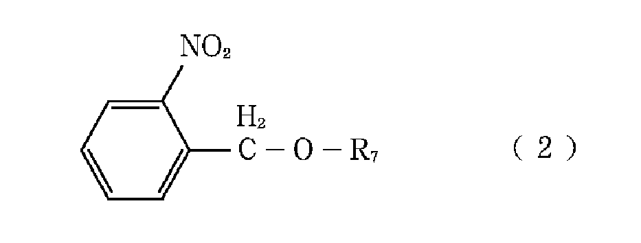
- The photosensitive compound according to claim 1, wherein the photosensitive compound has two or more structural units represented by General Formula (3) in the molecule:

- The photosensitive compound according to claim 1, wherein the photosensitive compound has two or more structural units represented by General Formula (4) in the molecule:

- The photosensitive compound according to claim 1, wherein the photosensitive compound has two or more structural units represented by General Formula (5) in the molecule:
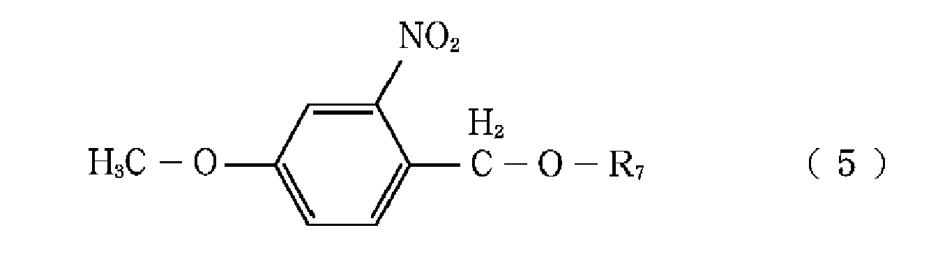
- A photosensitive compound having, in the molecule, two or more structural units represented by General Formula (6):

- The photosensitive compound according to claim 6, wherein the photosensitive compound has two or more structural units represented by General Formula (7) in the molecule:

- The photosensitive compound according to claim 6, wherein the photosensitive compound has two or more structural units represented by General Formula (8) in the molecule:

- The photosensitive compound according to claim 6, wherein the photosensitive compound has two or more structural units represented by General Formula (9) in the molecule:

- The photosensitive compound according to claim 6, wherein the photosensitive compound has two or more structural units represented by General Formula (10) in the molecule:

- A poly(hydroxystyrene) in which hydrogen atoms of two or more hydroxyl groups are substituted by the substituent represented by General Formula (11) or (12):


- A calixarene in which hydrogen atoms of two or more phenolic hydroxyl groups are substituted by the substituent represented by General Formula (11) or (12):
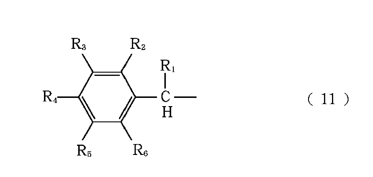

- A novolak resin in which in which hydrogen atoms of two or more phenolic hydroxyl groups are substituted by the substituent represented by General Formula (11) or (12):
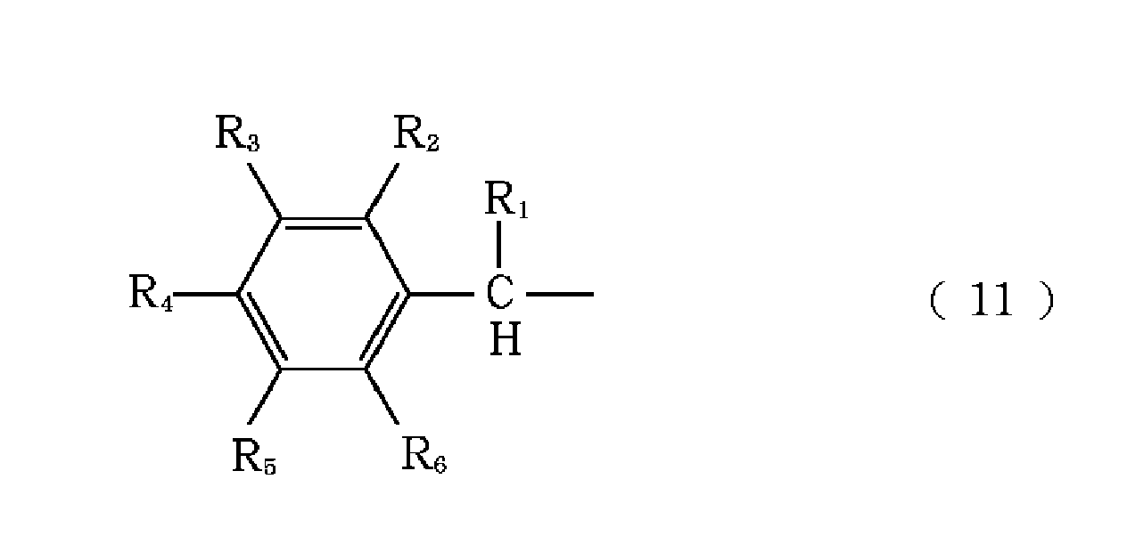
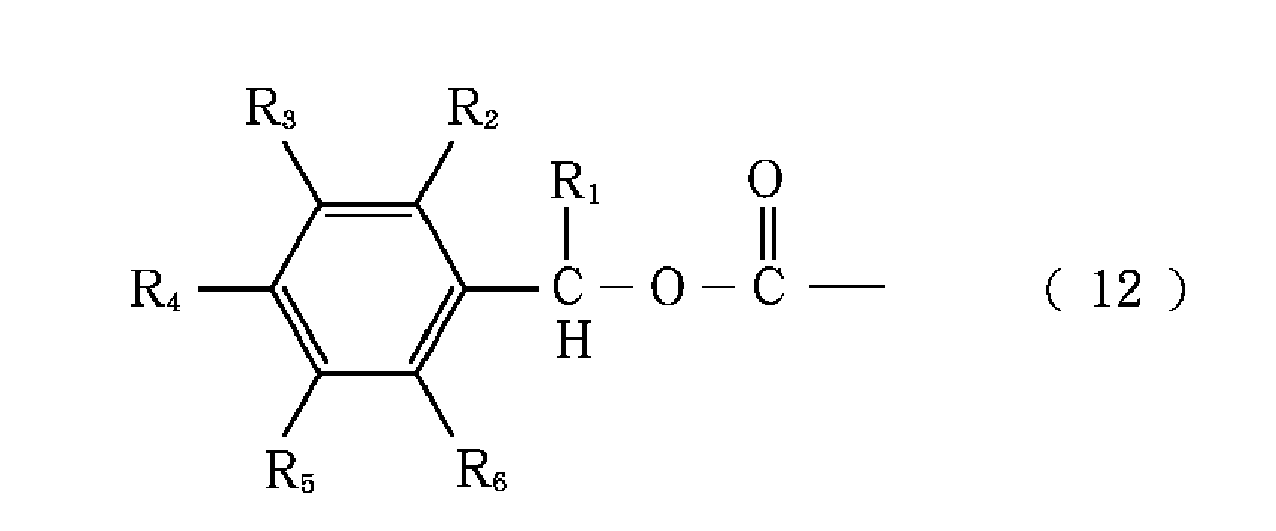
- A photosensitive composition comprising at least one of the compounds set forth in claims 1 to 13 dissolved in an organic solvent.
- A process for forming a resist pattern comprising the steps of:applying the photosensitive composition set forth in claim 14 on a substrate to form a photosensitive resist layer,irradiating the resist layer selectively with a radiation ray, anddeveloping a portion irradiated by the ray to form a pattern of the resist layer.
- The process for forming a resist pattern according to claim 15, wherein a resist layer capable of being removed by plasma etching and another resist layer resistant to plasma etching are laminated, and the photosensitive resist layer is formed on the layer resistant to plasma etching.
- The process for forming a resist pattern according to claim 15, wherein the photosensitive resist layer is formed in a thickness not more than 20 nm.
- The process for forming a resist pattern according to claim 15, wherein the irradiation of the radiation ray is conducted with near-field light.
- A process for producing a device, in which the device is formed on a substrate by the process for forming a resist pattern set forth in claim 15.
Applications Claiming Priority (2)
| Application Number | Priority Date | Filing Date | Title |
|---|---|---|---|
| JP2006161524 | 2006-06-09 | ||
| JP2007027368A JP5137410B2 (en) | 2006-06-09 | 2007-02-06 | Photosensitive compound, photosensitive composition, resist pattern forming method and substrate processing method |
Publications (2)
| Publication Number | Publication Date |
|---|---|
| EP1865379A1 true EP1865379A1 (en) | 2007-12-12 |
| EP1865379B1 EP1865379B1 (en) | 2013-01-16 |
Family
ID=38937638
Family Applications (1)
| Application Number | Title | Priority Date | Filing Date |
|---|---|---|---|
| EP07108733A Not-in-force EP1865379B1 (en) | 2006-06-09 | 2007-05-23 | Method for resist pattern formation, and process for device prodution |
Country Status (6)
| Country | Link |
|---|---|
| US (1) | US7651834B2 (en) |
| EP (1) | EP1865379B1 (en) |
| JP (1) | JP5137410B2 (en) |
| KR (1) | KR100922923B1 (en) |
| CN (1) | CN101086618B (en) |
| TW (1) | TWI399613B (en) |
Families Citing this family (14)
| Publication number | Priority date | Publication date | Assignee | Title |
|---|---|---|---|---|
| US7615332B2 (en) * | 2007-02-06 | 2009-11-10 | Canon Kabushiki Kaisha | Photosensitive compound, photosensitive composition, resist pattern forming method, and device production process |
| US7776509B2 (en) * | 2007-02-06 | 2010-08-17 | Canon Kabushiki Kaisha | Photosensitive compound, photosensitive composition, resist pattern forming method, and device production process |
| JP2008201724A (en) * | 2007-02-20 | 2008-09-04 | Canon Inc | Photosensitive compound, photosensitive composition, resist pattern forming method and substrate processing method |
| US7943285B2 (en) * | 2007-03-13 | 2011-05-17 | Panasonic Corporation | Pattern formation method |
| JP5262651B2 (en) * | 2008-12-05 | 2013-08-14 | Jsr株式会社 | Positive resist pattern forming method and developer for forming positive resist pattern |
| JP5262650B2 (en) * | 2008-12-05 | 2013-08-14 | Jsr株式会社 | Positive resist pattern forming method and developer for forming positive resist pattern |
| JP5627195B2 (en) * | 2009-04-27 | 2014-11-19 | 東海旅客鉄道株式会社 | Photosensitive composition, photosensitive metal complex, coating solution, and method for producing metal oxide thin film pattern |
| CN101942046A (en) * | 2010-09-15 | 2011-01-12 | 重庆大学 | Benzophenone fragment and p-nitrodiphenylethene fragment-containing tree like visible light photoinitiator and synthesis and application thereof |
| JP6093590B2 (en) * | 2013-02-20 | 2017-03-08 | 東京応化工業株式会社 | Method for manufacturing structure including phase separation structure, and method for forming guide pattern |
| KR20220115399A (en) * | 2021-02-10 | 2022-08-17 | 삼성전자주식회사 | Photoresist composition and method of manufacturing integrated circuit device using the same |
| US12265332B2 (en) * | 2021-06-18 | 2025-04-01 | Taiwan Semiconductor Manufacturing Company, Ltd. | Method of manufacturing a semiconductor device |
| JP2024010654A (en) * | 2022-07-12 | 2024-01-24 | 信越化学工業株式会社 | Positive resist material and pattern forming method |
| CN115407608B (en) * | 2022-08-22 | 2024-10-18 | 中国科学院光电技术研究所 | I-line single-component photoresist composition, preparation method and pattern forming method thereof |
| CN115826356A (en) * | 2022-12-13 | 2023-03-21 | Tcl华星光电技术有限公司 | Photoresist, display panel and manufacturing method thereof |
Citations (4)
| Publication number | Priority date | Publication date | Assignee | Title |
|---|---|---|---|---|
| JPS6269263A (en) | 1985-09-24 | 1987-03-30 | Toshiba Corp | Photosensitive composition |
| JPS62223156A (en) * | 1986-03-25 | 1987-10-01 | Wakayama Pref Gov | Novel derivative of calixarene and production thereof |
| EP0962825A1 (en) | 1997-12-19 | 1999-12-08 | Kansai Research Institute (KRI) | Photosensitive resin composition and process for producing the same |
| EP1033624A1 (en) | 1998-08-07 | 2000-09-06 | Clariant International Ltd. | Radiation-sensitive composition of chemical amplification type |
Family Cites Families (18)
| Publication number | Priority date | Publication date | Assignee | Title |
|---|---|---|---|---|
| JPS61185741A (en) * | 1985-02-13 | 1986-08-19 | Mitsubishi Chem Ind Ltd | Positive photoresist composition |
| JPS6225744A (en) * | 1985-07-26 | 1987-02-03 | Hitachi Ltd | Method of forming composite resist layer |
| JPS63146029A (en) | 1986-12-10 | 1988-06-18 | Toshiba Corp | Photosensitive composition |
| JPS63146038A (en) * | 1986-12-10 | 1988-06-18 | Toshiba Corp | Photosensitive composition |
| JPH01233447A (en) * | 1988-03-15 | 1989-09-19 | Oki Electric Ind Co Ltd | Photosensitive composition |
| JPH03141357A (en) * | 1989-10-27 | 1991-06-17 | Kanegafuchi Chem Ind Co Ltd | Photosensitive amphiphilic polymer compound and its production |
| US5314782A (en) * | 1993-03-05 | 1994-05-24 | Morton International, Inc. | Deep UV sensitive resistant to latent image decay comprising a diazonaphthoquinone sulfonate of a nitrobenzyl derivative |
| JPH11322656A (en) * | 1998-05-11 | 1999-11-24 | Jsr Corp | Novel calixarene derivative and calixresorcinarene derivative, and photosensitive composition |
| US6899999B2 (en) * | 2001-03-28 | 2005-05-31 | Kabushiki Kaisha Toshiba | Method of manufacturing composite member, photosensitive composition, porous base material, insulating body and composite member |
| JP2003066600A (en) * | 2001-06-12 | 2003-03-05 | Canon Inc | Photoresist, substrate processing method using the same, and photoresist manufacturing method |
| JP4156858B2 (en) * | 2002-04-03 | 2008-09-24 | 岡本化学工業株式会社 | Silane coupling agent |
| JP2005070319A (en) * | 2003-08-22 | 2005-03-17 | Canon Inc | Photoresist for near-field exposure and method for producing fine pattern using the same |
| JP4417090B2 (en) * | 2003-12-12 | 2010-02-17 | 株式会社ルネサステクノロジ | Pattern forming method, mask and exposure apparatus |
| US20050221222A1 (en) * | 2004-03-22 | 2005-10-06 | Canon Kabushiki Kaisha | Photosensitive resin composition, resist pattern forming method, substrate processing method, and device manufacturing method |
| JP2006013216A (en) * | 2004-06-28 | 2006-01-12 | Canon Inc | Method of forming resist pattern by near-field exposure, substrate processing method using the resist pattern forming method, and device manufacturing method |
| JP2006019447A (en) * | 2004-06-30 | 2006-01-19 | Canon Inc | Resist pattern forming method, substrate processing method, and device manufacturing method |
| JP2006071913A (en) * | 2004-09-01 | 2006-03-16 | Chiba Univ | Method for forming resist pattern |
| JP5013723B2 (en) * | 2006-03-09 | 2012-08-29 | キヤノン株式会社 | Fine particle pattern forming method and device manufacturing method |
-
2007
- 2007-02-06 JP JP2007027368A patent/JP5137410B2/en not_active Expired - Fee Related
- 2007-05-10 US US11/746,747 patent/US7651834B2/en not_active Expired - Fee Related
- 2007-05-23 EP EP07108733A patent/EP1865379B1/en not_active Not-in-force
- 2007-06-01 TW TW096119820A patent/TWI399613B/en not_active IP Right Cessation
- 2007-06-07 KR KR1020070055326A patent/KR100922923B1/en not_active Expired - Fee Related
- 2007-06-08 CN CN2007101103132A patent/CN101086618B/en not_active Expired - Fee Related
Patent Citations (4)
| Publication number | Priority date | Publication date | Assignee | Title |
|---|---|---|---|---|
| JPS6269263A (en) | 1985-09-24 | 1987-03-30 | Toshiba Corp | Photosensitive composition |
| JPS62223156A (en) * | 1986-03-25 | 1987-10-01 | Wakayama Pref Gov | Novel derivative of calixarene and production thereof |
| EP0962825A1 (en) | 1997-12-19 | 1999-12-08 | Kansai Research Institute (KRI) | Photosensitive resin composition and process for producing the same |
| EP1033624A1 (en) | 1998-08-07 | 2000-09-06 | Clariant International Ltd. | Radiation-sensitive composition of chemical amplification type |
Non-Patent Citations (2)
| Title |
|---|
| J. ORG. CHEM., vol. 68, 2003, pages 9100 |
| NISHIKUBO TADATOMI ET AL: "Study of photopolymers. XXXIV. Etherification and esterification reactions of polymers with (o, m, or p)-bromomethylnitrobenzene using the DBU method and the photochemical properties of the resulting polymers", J POLYM SCI PART A; JOURNAL OF POLYMER SCIENCE, PART A: POLYMER CHEMISTRY JAN 15 1990, vol. 28, no. 1, 15 January 1990 (1990-01-15), pages 105 - 117, XP002441517 * |
Also Published As
| Publication number | Publication date |
|---|---|
| JP5137410B2 (en) | 2013-02-06 |
| CN101086618B (en) | 2012-06-20 |
| KR100922923B1 (en) | 2009-10-22 |
| EP1865379B1 (en) | 2013-01-16 |
| TWI399613B (en) | 2013-06-21 |
| KR20070118016A (en) | 2007-12-13 |
| US7651834B2 (en) | 2010-01-26 |
| US20070287105A1 (en) | 2007-12-13 |
| TW200815913A (en) | 2008-04-01 |
| JP2008013745A (en) | 2008-01-24 |
| CN101086618A (en) | 2007-12-12 |
Similar Documents
| Publication | Publication Date | Title |
|---|---|---|
| EP1865379B1 (en) | Method for resist pattern formation, and process for device prodution | |
| JP2700918B2 (en) | Positive photoresist composition | |
| US7615332B2 (en) | Photosensitive compound, photosensitive composition, resist pattern forming method, and device production process | |
| JPH0651519A (en) | Positive photosensitive composition | |
| US7776509B2 (en) | Photosensitive compound, photosensitive composition, resist pattern forming method, and device production process | |
| JPH06266109A (en) | Positive photosensitive composition | |
| KR20220106794A (en) | chemically amplified photoresist | |
| KR102864915B1 (en) | PAG-free positive chemically amplified resist composition and method of using the same | |
| US7932014B2 (en) | Photosensitive compound, photosensitive composition, resist pattern forming method, and device production process | |
| JPH07271037A (en) | Positive ionization-sensitive radioactive resin composition | |
| JPH06130670A (en) | Positive photosensitive composition | |
| JPH06266107A (en) | Positive photosensitive composition | |
| JP3259263B2 (en) | Negative radiation-sensitive resin composition | |
| JPH06273924A (en) | Positive photosensitive composition | |
| JPH0962006A (en) | Positive type photoresist composition | |
| JPH08314142A (en) | Acid catalyst positive resist | |
| JPH08339075A (en) | Radiation sensitive resin composition | |
| JPH05134411A (en) | Negative resist composition | |
| JPH0934105A (en) | Positive type photosensitive composition |
Legal Events
| Date | Code | Title | Description |
|---|---|---|---|
| PUAI | Public reference made under article 153(3) epc to a published international application that has entered the european phase |
Free format text: ORIGINAL CODE: 0009012 |
|
| AK | Designated contracting states |
Kind code of ref document: A1 Designated state(s): AT BE BG CH CY CZ DE DK EE ES FI FR GB GR HU IE IS IT LI LT LU LV MC MT NL PL PT RO SE SI SK TR |
|
| AX | Request for extension of the european patent |
Extension state: AL BA HR MK YU |
|
| 17P | Request for examination filed |
Effective date: 20080612 |
|
| AKX | Designation fees paid |
Designated state(s): AT BE BG CH CY CZ DE DK EE ES FI FR GB GR HU IE IS IT LI LT LU LV MC MT NL PL PT RO SE SI SK TR |
|
| 17Q | First examination report despatched |
Effective date: 20110620 |
|
| GRAP | Despatch of communication of intention to grant a patent |
Free format text: ORIGINAL CODE: EPIDOSNIGR1 |
|
| RIN1 | Information on inventor provided before grant (corrected) |
Inventor name: ITO, TOSHIKI Inventor name: YAMAGUCHI, TAKAKO |
|
| GRAS | Grant fee paid |
Free format text: ORIGINAL CODE: EPIDOSNIGR3 |
|
| GRAA | (expected) grant |
Free format text: ORIGINAL CODE: 0009210 |
|
| AK | Designated contracting states |
Kind code of ref document: B1 Designated state(s): AT BE BG CH CY CZ DE DK EE ES FI FR GB GR HU IE IS IT LI LT LU LV MC MT NL PL PT RO SE SI SK TR |
|
| REG | Reference to a national code |
Ref country code: GB Ref legal event code: FG4D |
|
| REG | Reference to a national code |
Ref country code: CH Ref legal event code: EP |
|
| REG | Reference to a national code |
Ref country code: IE Ref legal event code: FG4D |
|
| REG | Reference to a national code |
Ref country code: AT Ref legal event code: REF Ref document number: 594169 Country of ref document: AT Kind code of ref document: T Effective date: 20130215 Ref country code: CH Ref legal event code: EP |
|
| REG | Reference to a national code |
Ref country code: DE Ref legal event code: R096 Ref document number: 602007028049 Country of ref document: DE Effective date: 20130314 |
|
| REG | Reference to a national code |
Ref country code: AT Ref legal event code: MK05 Ref document number: 594169 Country of ref document: AT Kind code of ref document: T Effective date: 20130116 |
|
| REG | Reference to a national code |
Ref country code: NL Ref legal event code: VDEP Effective date: 20130116 |
|
| REG | Reference to a national code |
Ref country code: LT Ref legal event code: MG4D |
|
| PG25 | Lapsed in a contracting state [announced via postgrant information from national office to epo] |
Ref country code: BE Free format text: LAPSE BECAUSE OF FAILURE TO SUBMIT A TRANSLATION OF THE DESCRIPTION OR TO PAY THE FEE WITHIN THE PRESCRIBED TIME-LIMIT Effective date: 20130116 Ref country code: ES Free format text: LAPSE BECAUSE OF FAILURE TO SUBMIT A TRANSLATION OF THE DESCRIPTION OR TO PAY THE FEE WITHIN THE PRESCRIBED TIME-LIMIT Effective date: 20130427 Ref country code: SE Free format text: LAPSE BECAUSE OF FAILURE TO SUBMIT A TRANSLATION OF THE DESCRIPTION OR TO PAY THE FEE WITHIN THE PRESCRIBED TIME-LIMIT Effective date: 20130116 Ref country code: BG Free format text: LAPSE BECAUSE OF FAILURE TO SUBMIT A TRANSLATION OF THE DESCRIPTION OR TO PAY THE FEE WITHIN THE PRESCRIBED TIME-LIMIT Effective date: 20130416 Ref country code: CY Free format text: LAPSE BECAUSE OF FAILURE TO SUBMIT A TRANSLATION OF THE DESCRIPTION OR TO PAY THE FEE WITHIN THE PRESCRIBED TIME-LIMIT Effective date: 20130116 Ref country code: AT Free format text: LAPSE BECAUSE OF FAILURE TO SUBMIT A TRANSLATION OF THE DESCRIPTION OR TO PAY THE FEE WITHIN THE PRESCRIBED TIME-LIMIT Effective date: 20130116 Ref country code: IS Free format text: LAPSE BECAUSE OF FAILURE TO SUBMIT A TRANSLATION OF THE DESCRIPTION OR TO PAY THE FEE WITHIN THE PRESCRIBED TIME-LIMIT Effective date: 20130516 Ref country code: LT Free format text: LAPSE BECAUSE OF FAILURE TO SUBMIT A TRANSLATION OF THE DESCRIPTION OR TO PAY THE FEE WITHIN THE PRESCRIBED TIME-LIMIT Effective date: 20130116 |
|
| PG25 | Lapsed in a contracting state [announced via postgrant information from national office to epo] |
Ref country code: GR Free format text: LAPSE BECAUSE OF FAILURE TO SUBMIT A TRANSLATION OF THE DESCRIPTION OR TO PAY THE FEE WITHIN THE PRESCRIBED TIME-LIMIT Effective date: 20130417 Ref country code: FI Free format text: LAPSE BECAUSE OF FAILURE TO SUBMIT A TRANSLATION OF THE DESCRIPTION OR TO PAY THE FEE WITHIN THE PRESCRIBED TIME-LIMIT Effective date: 20130116 Ref country code: LV Free format text: LAPSE BECAUSE OF FAILURE TO SUBMIT A TRANSLATION OF THE DESCRIPTION OR TO PAY THE FEE WITHIN THE PRESCRIBED TIME-LIMIT Effective date: 20130116 Ref country code: PT Free format text: LAPSE BECAUSE OF FAILURE TO SUBMIT A TRANSLATION OF THE DESCRIPTION OR TO PAY THE FEE WITHIN THE PRESCRIBED TIME-LIMIT Effective date: 20130516 Ref country code: PL Free format text: LAPSE BECAUSE OF FAILURE TO SUBMIT A TRANSLATION OF THE DESCRIPTION OR TO PAY THE FEE WITHIN THE PRESCRIBED TIME-LIMIT Effective date: 20130116 Ref country code: SI Free format text: LAPSE BECAUSE OF FAILURE TO SUBMIT A TRANSLATION OF THE DESCRIPTION OR TO PAY THE FEE WITHIN THE PRESCRIBED TIME-LIMIT Effective date: 20130116 Ref country code: NL Free format text: LAPSE BECAUSE OF FAILURE TO SUBMIT A TRANSLATION OF THE DESCRIPTION OR TO PAY THE FEE WITHIN THE PRESCRIBED TIME-LIMIT Effective date: 20130116 |
|
| PG25 | Lapsed in a contracting state [announced via postgrant information from national office to epo] |
Ref country code: CZ Free format text: LAPSE BECAUSE OF FAILURE TO SUBMIT A TRANSLATION OF THE DESCRIPTION OR TO PAY THE FEE WITHIN THE PRESCRIBED TIME-LIMIT Effective date: 20130116 Ref country code: RO Free format text: LAPSE BECAUSE OF FAILURE TO SUBMIT A TRANSLATION OF THE DESCRIPTION OR TO PAY THE FEE WITHIN THE PRESCRIBED TIME-LIMIT Effective date: 20130116 Ref country code: DK Free format text: LAPSE BECAUSE OF FAILURE TO SUBMIT A TRANSLATION OF THE DESCRIPTION OR TO PAY THE FEE WITHIN THE PRESCRIBED TIME-LIMIT Effective date: 20130116 Ref country code: EE Free format text: LAPSE BECAUSE OF FAILURE TO SUBMIT A TRANSLATION OF THE DESCRIPTION OR TO PAY THE FEE WITHIN THE PRESCRIBED TIME-LIMIT Effective date: 20130116 Ref country code: SK Free format text: LAPSE BECAUSE OF FAILURE TO SUBMIT A TRANSLATION OF THE DESCRIPTION OR TO PAY THE FEE WITHIN THE PRESCRIBED TIME-LIMIT Effective date: 20130116 |
|
| PLBE | No opposition filed within time limit |
Free format text: ORIGINAL CODE: 0009261 |
|
| STAA | Information on the status of an ep patent application or granted ep patent |
Free format text: STATUS: NO OPPOSITION FILED WITHIN TIME LIMIT |
|
| 26N | No opposition filed |
Effective date: 20131017 |
|
| PG25 | Lapsed in a contracting state [announced via postgrant information from national office to epo] |
Ref country code: IT Free format text: LAPSE BECAUSE OF FAILURE TO SUBMIT A TRANSLATION OF THE DESCRIPTION OR TO PAY THE FEE WITHIN THE PRESCRIBED TIME-LIMIT Effective date: 20130116 Ref country code: MC Free format text: LAPSE BECAUSE OF FAILURE TO SUBMIT A TRANSLATION OF THE DESCRIPTION OR TO PAY THE FEE WITHIN THE PRESCRIBED TIME-LIMIT Effective date: 20130116 |
|
| REG | Reference to a national code |
Ref country code: CH Ref legal event code: PL |
|
| GBPC | Gb: european patent ceased through non-payment of renewal fee |
Effective date: 20130523 |
|
| PG25 | Lapsed in a contracting state [announced via postgrant information from national office to epo] |
Ref country code: CH Free format text: LAPSE BECAUSE OF NON-PAYMENT OF DUE FEES Effective date: 20130531 Ref country code: LI Free format text: LAPSE BECAUSE OF NON-PAYMENT OF DUE FEES Effective date: 20130531 |
|
| REG | Reference to a national code |
Ref country code: DE Ref legal event code: R097 Ref document number: 602007028049 Country of ref document: DE Effective date: 20131017 |
|
| REG | Reference to a national code |
Ref country code: IE Ref legal event code: MM4A |
|
| REG | Reference to a national code |
Ref country code: FR Ref legal event code: ST Effective date: 20140131 |
|
| PG25 | Lapsed in a contracting state [announced via postgrant information from national office to epo] |
Ref country code: IE Free format text: LAPSE BECAUSE OF NON-PAYMENT OF DUE FEES Effective date: 20130523 Ref country code: GB Free format text: LAPSE BECAUSE OF NON-PAYMENT OF DUE FEES Effective date: 20130523 |
|
| PG25 | Lapsed in a contracting state [announced via postgrant information from national office to epo] |
Ref country code: FR Free format text: LAPSE BECAUSE OF NON-PAYMENT OF DUE FEES Effective date: 20130531 |
|
| PG25 | Lapsed in a contracting state [announced via postgrant information from national office to epo] |
Ref country code: MT Free format text: LAPSE BECAUSE OF FAILURE TO SUBMIT A TRANSLATION OF THE DESCRIPTION OR TO PAY THE FEE WITHIN THE PRESCRIBED TIME-LIMIT Effective date: 20130116 |
|
| PG25 | Lapsed in a contracting state [announced via postgrant information from national office to epo] |
Ref country code: TR Free format text: LAPSE BECAUSE OF FAILURE TO SUBMIT A TRANSLATION OF THE DESCRIPTION OR TO PAY THE FEE WITHIN THE PRESCRIBED TIME-LIMIT Effective date: 20130116 |
|
| PG25 | Lapsed in a contracting state [announced via postgrant information from national office to epo] |
Ref country code: HU Free format text: LAPSE BECAUSE OF FAILURE TO SUBMIT A TRANSLATION OF THE DESCRIPTION OR TO PAY THE FEE WITHIN THE PRESCRIBED TIME-LIMIT; INVALID AB INITIO Effective date: 20070523 Ref country code: LU Free format text: LAPSE BECAUSE OF NON-PAYMENT OF DUE FEES Effective date: 20130523 |
|
| PGFP | Annual fee paid to national office [announced via postgrant information from national office to epo] |
Ref country code: DE Payment date: 20160531 Year of fee payment: 10 |
|
| REG | Reference to a national code |
Ref country code: DE Ref legal event code: R119 Ref document number: 602007028049 Country of ref document: DE |
|
| PG25 | Lapsed in a contracting state [announced via postgrant information from national office to epo] |
Ref country code: DE Free format text: LAPSE BECAUSE OF NON-PAYMENT OF DUE FEES Effective date: 20171201 |