EP1860920A1 - Beleuchtungsvorrichtung mit einer Lichtquelle und einer Tastvorrichtung und Verfahren zum Betreiben einer derartigen Beleuchtungsvorrichtung - Google Patents
Beleuchtungsvorrichtung mit einer Lichtquelle und einer Tastvorrichtung und Verfahren zum Betreiben einer derartigen Beleuchtungsvorrichtung Download PDFInfo
- Publication number
- EP1860920A1 EP1860920A1 EP06010545A EP06010545A EP1860920A1 EP 1860920 A1 EP1860920 A1 EP 1860920A1 EP 06010545 A EP06010545 A EP 06010545A EP 06010545 A EP06010545 A EP 06010545A EP 1860920 A1 EP1860920 A1 EP 1860920A1
- Authority
- EP
- European Patent Office
- Prior art keywords
- output
- time constant
- lighting device
- input
- flop
- Prior art date
- Legal status (The legal status is an assumption and is not a legal conclusion. Google has not performed a legal analysis and makes no representation as to the accuracy of the status listed.)
- Granted
Links
Images


Classifications
-
- H—ELECTRICITY
- H05—ELECTRIC TECHNIQUES NOT OTHERWISE PROVIDED FOR
- H05B—ELECTRIC HEATING; ELECTRIC LIGHT SOURCES NOT OTHERWISE PROVIDED FOR; CIRCUIT ARRANGEMENTS FOR ELECTRIC LIGHT SOURCES, IN GENERAL
- H05B45/00—Circuit arrangements for operating light-emitting diodes [LED]
- H05B45/30—Driver circuits
- H05B45/32—Pulse-control circuits
Definitions
- the present invention relates to a lighting device with a light source and a touch device, which comprises a button, a connection for a supply voltage and a D flip-flop, wherein the D flip-flop a set input, a reset input, a clock Input, a data input, a Q output and a Qbar output, where the light source is connected to the Q output or the Qbar output. It also relates to a method for operating such a lighting device.
- Fig. 1 shows a sensing device comprising a button T1, in particular a changeover switch, and two pull-up resistors R1, R2 and two cross-coupled NAND gates, which together form an R / S flip-flop.
- the light source not shown, is to be coupled to the output A, for example directly or via a switching transistor or an electronic switching element.
- the main disadvantage of this probe device shown in Fig. 1 is that the button T1 must be multi-pole, ie as a switch, must be formed, which is too expensive for a variety of applications.
- the sensing device shown in FIG. 2 uses an RC element comprising the resistors R3, R4 and the capacitor C1 for debouncing. Furthermore, a pushbutton T2 and an inverter I1 are used. For the dimensioning of the RC element, the bounce time of the button T2 must be known. The RC element must be matched to the T2 button and the switching thresholds of the I1 inverter, so that debouncing works reliably. If, in fact, the RC element is too short, ie dimensioned with too short a time constant, the feeler device switches again when bouncing. A too slow dimensioning results in an undesirable dead time.
- the design for fast switching operations which is characterized by the use of a small-sized capacitor C, is sensitive to RF couplings on the switch leads and due to a shift of the trigger threshold voltage dips of the supply voltage U v , for example, load changes.
- the present invention is therefore based on the object, the above-mentioned lighting device such that it avoids the disadvantages of the prior art and in particular by a cost-effective implementation and characterized in that a reliable debouncing can be ensured regardless of the bounce time.
- Another object of the invention is to provide a corresponding method for operating a lighting device mentioned above.
- the invention is based on the finding that these objects can be achieved if a first timer with a first time constant and a second timer with a second time constant are used, the second time constant being greater than the first time constant.
- the first timer is connected on the one hand via the button to the connection for the supply voltage and on the other hand to the clock input.
- the second timer is coupled between the Qbar output and the data input. If the D flip-flop is in the reset state, pressing the button over the first timer generates a pulse-shaped voltage signal, which is applied to the clock input of the D flip-flop. The first rising edge of this signal triggers the D flip-flop, i. H.
- the level at the data input is polled synchronously with the pulse at the clock input and the Q output is switched to the level at the data input. Since in the reset state of the D flip-flop the Q output is low and the Qbar output is high, the high signal of the Qbar output is applied via the second timer to the data input of the D flip-flop created. In this "reset" state of the D flip-flop, the first pulse on the clock input triggers a switching operation of the D flip-flop, in which the signals at the Q output and Qbar output change. The Q output goes high, the Qbar output low. The data input initially remains at the previous level (High) due to the second time constant.
- the measure according to the invention effectively suppresses all pulse edges caused by trigger bounces, RF disturbances, voltage dips or load changes at the clock input.
- the debouncing is also independent of the impedance of the probe. It is insensitive to the amount of supply voltage, which is of particular importance for battery-powered systems but also for supply from power sources with higher output impedance, such as small power adapters.
- the implementation according to the invention is independent of the switching thresholds of the D flip-flops used. Because the first edge from low to high at the clock input triggers the D-flip-flop. Subsequent triggers are no longer accepted during the time period of the second time constant. From the first trigger on the clock input, this means a shift in the threshold due to the load change for subsequent pulses without any effect on the switching state of the D flip-flop.
- a particularly preferred embodiment is characterized in that the second time constant is at least 10 times, in particular at least 50 times, the first time constant. This variant ensures for a particularly long time that the data input remains at the high level until all the bounce pulses generated by pressing the button at the clock input of the D flip-flop have decayed safely.
- a third timer with a third time constant is provided, which is coupled between the connection for the supply voltage and the reset input. It is particularly preferred if the third time constant is at least 10 times, in particular at least 50 times, the first time constant. This ensures that a new reset pulse can be generated immediately after a shutdown or interruption of the supply voltage when restarting.
- At least one timer is implemented as an RC element and / or an LR element.
- RC elements or LR links are inexpensive to implement and easy to dimension.
- At least one timer comprises a first and a second ohmic resistor in series, wherein the first ohmic resistor, a capacitor is connected in parallel and the connection point between the first and the second ohmic resistor, the output and the point of departure facing away from this connection point between the first ohmic resistance and the capacitor represents the input of the respective timer.
- the set input is coupled to a reference potential, in particular to the ground potential.
- Fig. 3 shows an embodiment of a lighting device according to the invention in a schematic representation. It comprises a pushbutton T3, which is connected between the supply voltage connection U v and a first timer, which comprises the resistors R5, R6 and the capacitor C2 and with which a first time constant ⁇ 1 is realized.
- the resistor R5 and the capacitor C2 are connected in parallel, wherein the voltage drop across the resistor R6 is supplied to the clock input of a D flip-flop 10.
- the D flip-flop also has a reset input, a data input, a set input, a Q output and a Qbar output.
- the Qbar output is connected to the data input via a second timer comprising resistor R7 and capacitor C3, which together form a second time constant ⁇ 2.
- the set input is at a reference potential, in this case ground.
- the Q output represents a terminal A for connecting the light source La.
- the output A is coupled to the gate of a transistor T4 via a voltage divider comprising the resistors R10 and R11.
- the source terminal of the transistor T4 is connected to the ground terminal, while between the drain terminal and the supply voltage U v, the light source La is arranged, which in the present case comprises four series-connected LEDs.
- the light source could also be coupled directly to the output A.
- the reset input is connected to the supply voltage terminal U v via a third timer, which comprises the resistors R8 and R9 and the capacitor C4 and forms a third time constant ⁇ 3.
- the D-type flip-flop 10 is reset at startup of the lighting device. For this purpose, a single reset pulse is generated with the aid of the components R8, C4 and R9 when the supply voltage is switched on.
- the charging current generated at the resistor R9 a voltage drop, which is present as a signal at the reset input of the D flip-flop 10 and resets it.
- At the Q output of the reset D flip-flop 10 is a low signal, at the Qbar output corresponding to a high signal.
- a low voltage corresponding to the voltage divider from the resistors R8 and R9 sets at the reset input, for example, 0.1 * U v .
- the clock input of the D flip-flop 10 is enabled.
- a switching operation of the D-type flip-flop 10 can now take place when the pushbutton T3 is pressed.
- the data input initially remains at the previous level (high), since the capacitor C3 must first discharge via the resistor R7 with the time constant ⁇ 2. During this period of time, voltage pulses arriving at the clock input can not switch again since the data input is still at the high level. Due to the delayed due to the time constant ⁇ 2 level change at the data input all caused by Tasterprellen, RF interference, voltage dips or load changes pulse edges are effectively suppressed at the clock input.
- Debouncing is also insensitive to the level of the supply voltage.
- the switching threshold of the clock input of the D flip-flop must be exceeded by a pulse triggered by a switching operation of the button, at least once so that the flip-flop then - at the first such pulse - switches.
- the dimensioning of R5, C2, R6 ensures that this pulse triggered by the probe always has a sufficiently high amplitude to trigger a switching operation of the D flip-flop, even if the supply voltage U v is in a wide range, for example between 8 V and 18 V DC, varies.
- ⁇ 1 is 0.1 ms
- ⁇ 2 is 10 ms
- ⁇ 3 is 10 ms
- ⁇ 4 100 ms
- R10 is 100 ⁇
- R11 is 1 M ⁇ .
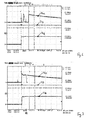
- FIGS. 4 to 7 show the time profiles of the signals at the clock input U C1 , at the data input U D and at the Q output U Q for an exemplary embodiment of a lighting device according to the invention, the time resolution in FIGS. 4 and 5 being 0 ms, in Figures 6 and 7 is 10.0 microseconds.
- Fig. 4 shows the time course of said three signals at a power-up after a reset. Over time, the voltage U Cl of the pulse generated by pressing the button T3 can be seen initially at time t1. This leads to a switching of the D flip-flops, as can be seen on the time course of the voltage U Q.
- the not shown voltage at the Qbar output changes in the opposite way, ie while U Q goes from low to high, U Qbar goes from high to low.
- the change in the voltage U Qbar at the output Qbar is only delayed given to the data input as a result of the time determined by the capacitor C3 and the resistor R7 time constant ⁇ 2, as well to be recognized by the time course of the voltage U D.
- Fig. 5 shows the time course of said signals at a turn-off of the D-type flip-flop 10.
- the D flip-flop 10 switches; the voltage U Q at the Q output goes from high to low.
- the voltage at the Qbar output changes in the opposite way, ie it goes from low to high. This change is in turn passed through the capacitor C3 and the resistor R7 fixed time constant ⁇ 2 only delayed to the data input, as well to recognize by the time course of the voltage U D.
- FIGS. 6 and 7 show the time profile of the signals mentioned in a significantly greater resolution, in each case during a switch-on process.
- the resolution is so great that the reduction in the amplitude of the voltage U D is barely discernible (which, however, in view of the Representation in Figures 6 and 7 is not relevant).
- FIG. 6 clearly shows that a key bounce, ie several successive pulses at the clock input, see the course of the voltage U C1 , reliably does not lead to a corresponding switching of the D flip-flop. This can be seen from the fact that the voltage U Q at the Q output does not change again after a first change, despite the sequence of pulses at the clock input. The reason is that at the time of the repeated pulses at the clock input, the data input is still high, see the corresponding amplitude of the voltage U D.
- FIG. 7 shows a further example: It should be pointed out here that, in the course of time of the voltage U C1, a distinctly pronounced second rising edge occurs at the clock input at the clock input t2. As can be seen in the time course of the voltage U Q at the Q output, this second rising edge does not lead to a renewed switching of the D flip-flop 10. The cause is in turn that at time t2 of the occurrence of the second rising edge, the voltage U D is still high at the signal input of the D flip-flop.
Landscapes
- Electronic Switches (AREA)
- Circuit Arrangement For Electric Light Sources In General (AREA)
- Push-Button Switches (AREA)
Abstract
Description
- Die vorliegende Erfindung betrifft eine Beleuchtungsvorrichtung mit einer Lichtquelle und einer Tastvorrichtung, die einen Taster, einen Anschluss für eine Versorgungsspannung und ein D-Flip-Flop umfasst, wobei das D-Flip-Flop einen Set-Eingang, einen Reset-Eingang, einen Clock-Eingang, einen Daten-Eingang, einen Q-Ausgang und einen Qbar-Ausgang aufweist, wobei, die Lichtquelle am Q-Ausgang oder am Qbar-Ausgang angeschlossen ist. Sie betrifft überdies ein Verfahren zum Betreiben einer derartigen Beleuchtungsvorrichtung.
- In modernen Leuchten kommen zunehmend flache Folientastvorrichtungen und flache Taster zum Einsatz, mit denen beispielsweise die Lichtquelle geschaltet oder gedimmt werden soll. Ein Problem hierbei stellt die Entprellung der Tastvorrichtung dar.
- Zwei aus dem Stand der Technik bekannte, für derartige Aufgaben eingesetzte Tastvorrichtungen sind in den Figuren 1 und 2 dargestellt.
- Fig. 1 zeigt eine Tastvorrichtung, die einen Taster T1, insbesondere einen Wechselschalter, umfasst sowie zwei Pull-Up-Widerstände R1, R2 und zwei über Kreuz gekoppelte NAND-Gatter, die zusammen ein R/S-FlipFlop bilden. Die nicht dargestellte Lichtquelle ist an den Ausgang A zu koppeln, beispielsweise direkt oder über einen Schalttransistor oder ein elektronisches Schaltelement. Der wesentliche Nachteil dieser in Fig. 1 dargestellten Tastvorrichtung besteht darin, dass der Taster T1 mehrpolig, d.h. als Umschalter, ausgebildet werden muss, was für eine Vielzahl von Anwendungen zu teuer ist.
- Die in Fig. 2 dargestellte Tastvorrichtung verwendet zur Entprellung ein RC-Glied, das die Widerstände R3, R4 und den Kondensator C1 umfasst. Weiterhin verwendet werden ein Taster T2 sowie ein Inverter I1. Zur Dimensionierung des RC-Glieds muss die Prellzeit des Tasters T2 bekannt sein. Das RC-Glied muss auf den Taster T2 und die Schaltschwellen des Inverters I1 abgestimmt sein, damit die Entprellung zuverlässig funktioniert. Ist nämlich das RC-Glied zu knapp, d.h. mit zu geringer Zeitkonstante, dimensioniert, schaltet die Tastvorrichtung bei einem Prellen nochmals. Bei einer zu langsamen Dimensionierung ergibt sich eine unerwünschte Totzeit. Da der Kondensator C1 analog aufgeladen wird, führt eine Änderung der Versorgungsspannung Uv zu einer Änderung der Ladezeit und damit der Zeitabstimmung des RC-Glieds . Die Auslegung für schnelle Schaltvorgänge, die sich durch Verwendung eines klein dimensionierten Kondensators C auszeichnet, reagiert empfindlich auf HF-Einkopplungen über die Schalterzuleitungen und infolge einer Verschiebung der Triggerschwelle auf Spannungseinbrüche der Versorgungsspannung Uv, beispielsweise bei Lastwechseln.
- Der vorliegenden Erfindung liegt deshalb die Aufgabe zugrunde, die eingangs genannte Beleuchtungsvorrichtung derart weiterzubilden, dass sie die Nachteile des Standes der Technik vermeidet und sich insbesondere durch eine kostengünstige Realisierung sowie dadurch auszeichnet, dass eine zuverlässige Entprellung unabhängig von der Prellzeit sichergestellt werden kann. Eine weitere Aufgabe der Erfindung besteht darin, ein entsprechendes Verfahren zum Betreiben einer eingangs genannten Beleuchtungsvorrichtung zur Verfügung zu stellen.
- Diese Aufgaben werden gelöst einerseits durch eine Beleuchtungsvorrichtung mit den Merkmalen von Patentanspruch 1, andererseits durch ein Verfahren mit den Merkmalen von Patentanspruch 9.
- Der Erfindung liegt die Erkenntnis zugrunde, dass diese Aufgaben gelöst werden können, wenn ein erstes Zeitglied mit einer ersten Zeitkonstante und ein zweites Zeitglied mit einer zweiten Zeitkonstante verwendet werden, wobei die zweite Zeitkonstante größer ist als die erste Zeitkonstante. Das erste Zeitglied wird einerseits über den Taster mit dem Anschluss für die Versorgungsspannung und andererseits mit dem Clock-Eingang verbunden. Das zweite Zeitglied wird zwischen den Qbar-Ausgang und den Daten-Eingang gekoppelt. Befindet sich das D-Flip-Flop im zurückgesetzten Zustand, wird durch ein Drücken des Tasters über das erste Zeitglied ein pulsförmiges Spannungssignal erzeugt, das an den Clock-Eingang des D-Flip-Flops gelegt wird. Durch die erste ansteigende Flanke dieses Signals wird das D-Flip-Flop getriggert, d. h. der Pegel am Daten-Eingang wird zeitlich synchron zum Puls am Clock-Eingang abgefragt und der Q-Ausgang wird auf den Pegel am Daten-Eingang geschaltet. Da beim D-Flip-Flop im zurückgesetzten Zustand der Q-Ausgang auf Low und der Qbar-Ausgang entsprechend auf High liegen, wird das High-Signal des Qbar-Ausgangs über das zweite Zeitglied an den Daten-Eingang des D-Flip-Flops angelegt. In diesem "zurückgesetzten" Zustand des D-Flip-Flops löst der erste Impuls am Clock-Eingang einen Umschaltvorgang des D-Flip-Flops aus, bei dem sich die Signale am Q-Ausgang und Qbar-Ausgang ändern. Der Q-Ausgang geht auf High, der Qbar-Ausgang auf Low. Der Daten-Eingang bleibt zunächst infolge der zweiten Zeitkonstante auf dem vorherigen Pegel (High). Während dieser, durch das zweite Zeitglied bestimmten Zeitspanne können weitere Spannungsimpulse, die am Clock-Eingang eintreffen, das D-Flip-Flop nicht nochmals umschalten, da der Daten-Eingang noch immer auf High liegt. Erst wenn der Daten-Eingang auf Low geht, d. h. nach Ablauf der zweiten Zeitkonstante, kann ein erneuter Schaltvorgang des D-Flip-Flops durchgeführt werden.
- Durch die erfindungsgemäße Maßnahme werden sämtliche durch Tasterprellen, HF-Störungen, Spannungseinbrüche oder Lastwechsel hervorgerufene Impulsflanken am Clock-Eingang wirksam unterdrückt. Durch die Verwendung eines schlichten Tasters - im Gegensatz zu einem mehrpoligen Taster mit Umschaltkontakt - ergibt sich eine einfache und kostengünstige Dimensionierung. Die Entprellung ist überdies unabhängig von der Impedanz des Tasters. Sie ist unempfindlich gegenüber der Höhe der Versorgungsspan-nung, was insbesondere für batteriebetriebene Systeme aber auch bei Versorgung aus Stromquellen mit höherer Ausgangsimpedanz, beispielsweise kleine Steckernetzteile, von außerordentlicher Bedeutung ist. Schließlich ist die erfindungsgemäße Realisierung unabhängig von den Schaltschwellen des verwendeten D-Flip-Flops. Denn die erste Flanke von Low nach High am Clock-Eingang triggert das D-Flip-Flop. Nachfolgende Trigger werden während der Zeitdauer der zweiten Zeitkonstante nicht mehr akzeptiert. Ab dem ersten Trigger am Clock-Eingang ist damit eine Verschiebung der Schwelle durch den Lastwechsel für nachfolgende Impulse ohne Auswirkung auf den Schaltzustand des D-Flip-Flops.
- Eine besonders bevorzugte Ausführungsform zeichnet sich dadurch aus, dass die zweite Zeitkonstante mindestens das 10-fache, insbesondere mindestens das 50-fache, der ersten Zeitkonstante beträgt. Diese Variante stellt besonders lange sicher, dass der Daten-Eingang solange auf dem High-Pegel bleibt, bis alle durch das Drücken des Tasters erzeugten Prellimpulse am Clock-Eingang des D-Flip-Flops sicher abgeklungen sind.
- Bevorzugt ist zum Zurücksetzen des D-Flip-Flops ein drittes Zeitglied mit einer dritten Zeitkonstante vorgesehen, das zwischen den Anschluss für die Versorgungsspannung und den Reset-Eingang gekoppelt ist. Besonders bevorzugt ist, wenn die dritte Zeitkonstante mindestens das 10-fache, insbesondere mindestens das 50-fache, der ersten Zeitkonstante beträgt. Dies stellt sicher, dass nach einer Abschaltung oder Unterbrechung der Versorgungsspannung bei einer erneuten Inbetriebnahme sofort ein neuer Reset-Impuls generiert werden kann.
- Bevorzugt ist mindestens ein Zeitglied, noch bevorzugter alle Zeitglieder, als RC-Glied und/oder LR-Glied ausgeführt. RC-Glieder bzw. LR-Glieder sind kostengünstig zu realisieren und einfach zu dimensionieren.
- Bevorzugt umfasst mindestens ein Zeitglied einen ersten und einen zweiten ohmschen Widerstand in Serienschaltung, wobei dem ersten ohmschen Widerstand ein Kondensator parallelgeschaltet ist und der Verbindungspunkt zwischen dem ersten und dem zweiten ohmschen Widerstand den Ausgang und der von diesem Verbindungspunkt abgekehrte Verbindungspunkt zwischen dem ersten ohmschen Widerstand und dem Kondensator den Eingang des jeweiligen Zeitglieds darstellt.
- Weiterhin bevorzugt ist der Set-Eingang mit einem Bezugspotential, insbesondere mit dem Massepotential, gekoppelt.
- Weitere vorteilhafte Ausführungsformen ergeben sich aus den Unteransprüchen.
- Die im Vorhergehenden mit Bezug auf die erfindungsgemäße Beleuchtungsvorrichtung genannten Vorteile sowie die erwähnten bevorzugten Ausführungsformen und deren Vorteile gelten entsprechend, soweit anwendbar, für das erfindungsgemäße Verfahren.
- Im Nachfolgenden wird nunmehr ein Ausführungsbeispiel einer erfindungsgemäßen Beleuchtungsvorrichtung unter Bezugnahme auf die beigefügten Zeichnungen näher beschrieben. Es zeigen:
- Fig. 1
- eine erste aus dem Stand der Technik bekannte, in einer Beleuchtungsvorrichtung verwendete Tastvorrichtung;
- Fig. 2
- eine zweite aus dem Stand der Technik bekannte, in einer Beleuchtungsvorrichtung verwendete Tastvorrichtung;
- Fig. 3
- ein Ausführungsbeispiel einer erfindungsgemäßen Beleuchtungsvorrichtung mit einer Lichtquelle und einer Tastvorrichtung;
- Fig. 4
- den zeitlichen Verlauf der Signale am Clock-Eingang, am Daten-Eingang und am Q-Ausgang bei einem Einschaltvorgang nach einem Reset;
- Fig. 5
- den zeitlichen Verlauf der Signale am Clock-Eingang, am DatenEingang und am Q-Ausgang bei einem Ausschaltvorgang;
- Fig. 6
- den zeitlichen Verlauf der Signale am Clock-Eingang, am Daten-Eingang und am Q-Ausgang bei einem Einschaltvorgang und Tasterprellen in vergrößerter Darstellung; und
- Fig. 7
- den zeitlichen Verlauf der Signale am Clock-Eingang, am Daten-Eingang und am Q-Ausgang bei einer durch Tasterprellen ausgelösten steigenden Flanke in vergrößerter Darstellung.
- Fig. 3 zeigt ein Ausführungsbeispiel einer erfindungsgemäßen Beleuchtungsvorrichtung in schematischer Darstellung. Sie umfasst einen Taster T3, der zwischen den Versorgungsspannungsanschluss Uv und ein erstes Zeitglied geschaltet ist, das die Widerstände R5, R6 und den Kondensator C2 umfasst und mit dem eine erste Zeitkonstante τ1 realisiert ist. Dabei sind der Widerstand R5 und der Kondensator C2 parallelgeschaltet, wobei die am Widerstand R6 abfallende Spannung dem Clock-Eingang eines D-Flip-Flops 10 zugeführt wird. Das D-Flip-Flop weist darüber hinaus einen Reset-Eingang, einen Daten-Eingang, einen Set-Eingang, einen Q-Ausgang sowie einen Qbar-Ausgang auf. Der Qbar-Ausgang ist über ein zweites Zeitglied, das den Widerstand R7 und den Kondensator C3 umfasst, die zusammen eine zweite Zeitkonstante τ2 bilden, mit dem Daten-Eingang verbunden. Der Set-Eingang liegt auf einem Bezugspotential, vorliegend Masse. Der Q-Ausgang stellt einen Anschluss A zum Anschließen der Lichtquelle La dar. Vorliegend ist der Ausgang A über einen Spannungsteiler, der die Widerstände R10 und R11 umfaßt, and das Gate eines Transistor T4 gekoppelt. Der Source-Anschluß des Transistors T4 ist mit dem Masseanschluß verbunden, während zwischen dem Drain-Anschluß und der Versorgungsspannung Uv die Lichtquelle La angeordnet ist, die vorliegend vier in Serie geschaltete LEDs umfasst. Anstelle des dargestellten Anschlusses der Lichtquelle La über ein elektronisches Schaltelement, vorliegend einen Transistor, könnte die Lichtquelle auch direkt an den Ausgang A gekoppelt sein. Der Reset-Eingang ist über ein drittes Zeitglied, das die Widerstände R8 und R9 sowie den Kondensator C4 umfasst und eine dritte Zeitkonstante τ3 bildet, mit dem Versorgungsspannungsanschluss Uv verbunden.
- Zunächst ist das D-Flip-Flop 10 bei Inbetriebnahme der Beleuchtungsvorrichtung zurückzusetzen. Dazu wird mit Hilfe der Bauelemente R8, C4 und R9 beim Einschalten der Versorgungsspannung ein einzelner Reset-Impuls generiert: Der zunächst entladene Kondensator C4 wird über den Widerstand R9 einmalig mit der Zeitkonstante τ3 = C4 * R9 aufgeladen. Der Ladestrom generiert am Widerstand R9 einen Spannungsabfall, der als Signal am Reset-Eingang des D-Flip-Flops 10 anliegt und diesen zurücksetzt. Am Q-Ausgang des zurückgesetzten D-Flip-Flops 10 liegt ein Low-Signal an, am Qbar-Ausgang entsprechend ein High-Signal. Nach Beendigung der Aufladung des Kondensators C4 stellt sich am Reset-Eingang eine niedrige Spannung entsprechend dem Spannungsteiler aus den Widerständen R8 und R9 ein, beispielsweise 0,1 * Uv. Wenn dieser Low-Pegel am Reset-Eingang anliegt, wird der Clock-Eingang des D-Flip-Flops 10 freigegeben.
- Bei Abschaltung oder Unterbrechung der Versorgungsspannung am Versorgungsspannungsanschluss Uv wird der Kondensator C4 über den Widerstand R8 mit einer vierten Zeitkonstante τ4 = C4 * R8 zügig entladen, so dass bei erneuter Inbetriebnahme sofort ein neuer Reset-Impuls generiert werden kann.
- Nach dem Zurücksetzen des D-Flip-Flops kann nunmehr ein Schaltvorgang des D-Flip-Flops 10 bei Drücken des Tasters T3 stattfinden. Im Einzelnen: Zunächst wird beim Drücken des Tasters T3 der Kondensator C2 über den -Widerstand R6 mit der Zeitkonstante τ1 = C2 * R6 aufgeladen. Durch den wegen des Tasterprellens pulsförmigen Ladestrom über dem Widerstand R6, fällt an diesem Widerstand eine pulsförmige Spannung ab, die am Clock-Eingang des D-Flip-Flops 10 anliegt. Die erste ansteigende Flanke dieses Signals triggert das D-Flip-Flop 10, d. h. der Pegel am Daten-Eingang wird zeitlich synchron zum Impuls am Clock-Eingang abgefragt und der Q-Ausgang wird auf den Pegel am Daten-Eingang geschaltet. Da nach dem Zurücksetzen des D-Flip-Flops der Q-Ausgang auf Low und der Qbar-Ausgang auf High liegt und nach τ3 = R7 * C3 am Daten-Eingang der High-Pegel des Qbar-Ausgangs anliegt, schaltet das D-Flip-Flop nach dem ersten Clock-Impuls (Einschaltvorgang) am Clock-Eingang und die Pegel der Ausgänge ändern sich: Der Q-Ausgang wird high und der Qbar-Ausgang wird low. Besonders von Bedeutung ist hierbei, dass der Daten-Eingang zunächst auf dem vorherigen Pegel (High) bleibt, da sich der Kondensator C3 erst über den Widerstand R7 mit der Zeitkonstante τ2 entladen muss. Während dieser Zeitspanne können nunmehr Spannungsimpulse, die am Clock-Eingang eintreffen, das D-Flip-Flop nicht wieder umschalten, da der Daten-Eingang noch immer auf dem High-Pegel liegt. Durch die infolge der Zeitkonstante τ2 verzögerte Pegeländerung am Daten-Eingang werden sämtliche durch Tasterprellen, HF-Störungen, Spannungseinbrüche oder Lastwechsel hervorgerufene Impulsflanken am Clock-Eingang wirksam unterdrückt.
- Erst wenn nach der Zeitkonstante τ2 der Pegel des Daten-Eingangs auf den Pegel am Qbar-Ausgang geht (vorliegend ist der Qbar-Ausgang auf Low), führt eine ansteigende Signalflanke am Clock-Eingang (Ausschaltvorgang) zum Umschalten des D-Flip-Flops 10. Der Pegel am Q-Ausgang ändert sich auf Low, der am Qbar-Ausgang auf High. Der Daten-Eingang bleibt zunächst auf dem vorherigen Pegel (Low), da sich der Kondensator C3 erst über R7 aufladen muss.
- Während dieser Zeitspanne können Spannungsimpulse, die am Clock-Eingang eintreffen, das D-Flip-Flop 10 nicht wieder umschalten. Durch die verzögerte Pegeländerung am Daten-Eingang infolge der Aufladung des Kondensators C3 über den Widerstand R7 werden sämtliche durch Tasterprellen, HF-Störungen, Spannungseinbrüche oder Lastwechsel hervorgerufene Impulsflanken am Clock-Eingang wirksam unterdrückt. Dabei ist die Entprellung unabhängig von der Impedanz des Tasters T1. Dies hat seine Ursache darin, dass die "ON"-Impedanz Ri des Tasters T1 klein ist, beispielsweise 30 Ω, im Vergleich zum Widerstand R6, beispielsweise 10 kΩ. Damit wird die Aufladung von C2, die der Summe aus R1 + R6 proportional ist, nur wenig von dem zusätzlichen Widerstand von Ri beeinflusst (10030 Ω anstelle von 10000 Ω). Die Entprellung ist überdies unempfindlich gegenüber der Höhe der Versorgungsspannung. Die Schaltschwelle des Clock-Eingangs des D-Flip-Flops muss durch einen Impuls, ausgelöst durch einen Schaltvorgang des Tasters, mindestens einmal überschritten werden, damit das Flip-Flop dann - beim ersten derartigen Impuls - schaltet. Durch die Dimensionierung von R5, C2, R6 ist gewährleistet, dass dieser durch den Taster ausgelöste Impuls immer eine hinreichend hohe Amplitude hat, um einen Schaltvorgang des D-Flip-Flops auszulösen, auch wenn die Versorgungsspannung Uv in einem weiten Bereich, beispielsweise zwischen 8 V und 18 V Gleichspannung, variiert.
- Erst wenn nach der Zeitkonstante τ2 auf den Pegel des Qbar-Ausgangs gegangen wird (in diesem Fall ist der Qbar-Ausgang auf High, was den Zustand nach dem Zurücksetzen des D-Flip-Flops entspricht), führt eine ansteigende Signalflanke am Clock-Eingang (Einschaltvorgang) zum Umschalten des D-Flip-Flops 10.
- Bedeutend für die vorliegende Erfindung ist, dass die erste Zeitkonstante τ1 = C2 * R6 kleiner ist als die zweite Zeitkonstante τ2 = C3 * R7. Die dritte Zeitkonstante τ3 = C4 * R9 liegt bevorzugt im Bereich zwischen 10 und 50 ms, damit kurze Spikes auf der Gleichstrom-Versorgung keinen RESET auslösen. In einem bevorzugten Ausführungsbeispiel beträgt τ1 0,1 ms, τ2 10 ms, τ3 10 ms, τ4 100 ms, R10 100 Ω und R11 1 MΩ.
- Die Figuren 4 bis 7 zeigen die zeitlichen Verläufe der Signale am Clock-Eingang UCl, am Daten-Eingang UD sowie am Q-Ausgang UQ für ein Ausführungsbeispiel einer erfindungsgemäßen Beleuchtungsvorrichtung, wobei die zeitliche Auflösung in den Figuren 4 und 5 20,0 ms, in den Figuren 6 und 7 10,0 µs beträgt. Fig. 4 zeigt den zeitlichen Verlauf der genannten drei Signale bei einem Einschaltvorgang nach einem Reset. Im zeitlichen Verlauf der Spannung UCl ist zunächst zum Zeitpunkt t1 der durch Drücken des Tasters T3 erzeugte Impuls zu erkennen. Dieser führt zu einem Umschalten des D-Flip-Flops, wie am zeitlichen Verlauf der Spannung UQ zu erkennen. Die nicht dargestellte Spannung am Qbar-Ausgang ändert sich in umgekehrter Weise, d. h. während UQ von Low auf High geht, geht UQbar von High auf Low. Die Änderung der Spannung UQbar am Ausgang Qbar wird infolge der durch den Kondensator C3 und dem Widerstand R7 bestimmten Zeitkonstante τ2 nur verzögert an den Daten-Eingang weitergegeben, wie durch den zeitlichen Verlauf der Spannung UD gut zu erkennen.
- Fig. 5 zeigt den zeitlichen Verlauf der genannten Signale bei einem Ausschaltvorgang des D-Flip-Flops 10. Im zeitlichen Verlauf der Spannung UCl am Clock-Eingang ist wiederum zum Zeitpunkt t1 das Drücken des Tasters T3 zu erkennen. Daraufhin schaltet das D-Flip-Flop 10; die Spannung UQ am Q-Ausgang geht von High auf Low. Die Spannung am Qbar-Ausgang ändert sich in umgekehrter Weise, d. h. sie geht von Low auf High. Diese Änderung wird wiederum durch den Kondensator C3 und den Widerstand R7 festgelegte Zeitkonstante τ2 nur verzögert an den Daten-Eingang weitergegeben, wie durch den zeitlichen Verlauf der Spannung UD gut zu erkennen.
- Wie bereits erwähnt, zeigen die Figuren 6 und 7 den zeitlichen Verlauf der genannten Signale in deutlich größerer Auflösung, jeweils bei einem Einschaltvorgang. Die Auflösung ist so groß, dass die Verkleinerung der Amplitude der Spannung UD kaum zu erkennen ist (was jedoch im Hinblick auf die Darstellung in den Figuren 6 und 7 ohne Relevanz ist). Zunächst zu Fig. 6: Fig. 6 zeigt deutlich, dass ein Tasterprellen, d. h. mehrere aufeinanderfolgende Impulse am Clock-Eingang, siehe den Verlauf der Spannung UCl, zuverlässig nicht zu einem entsprechenden Schalten des D-Flip-Flops führen. Dies ist daran zu erkennen, dass sich die Spannung UQ am Q-Ausgang trotz der Folge von Impulsen am Clock-Eingang nach einer ersten Änderung nicht nochmals ändert. Die Ursache liegt darin, dass zum Zeitpunkt der wiederholten Impulse am Clock-Eingang der Daten-Eingang noch immer auf High liegt, siehe die entsprechende Amplitude der Spannung UD.
- Fig. 7 zeigt ein weiteres Beispiel: Hier ist darauf hinzuweisen, dass im zeitlichen Verlauf der Spannung UCl am Clock-Eingang eine deutlich ausgeprägte zweite ansteigende Flanke zum Zeitpunkt t2 auftritt. Wie am zeitlichen Verlauf der Spannung UQ am Q-Ausgang zu erkennen ist, führt diese zweite ansteigende Flanke nicht zu einem erneuten Umschalten des D-Flip-Flops 10. Ursache ist wiederum, dass zum Zeitpunkt t2 des Auftretens der zweiten ansteigenden Flanke die Spannung UD am Signaleingang des D-Flip-Flops noch immer auf High ist.
Claims (9)
- Beleuchtungsvorrichtung mit einer Lichtquelle und einer Tastvorrichtung, die einen Taster, einen Anschluss für eine Versorgungsspannung und ein D-Flip-Flop (10) umfasst, wobei das D-Flip-Flop (10) einen Set-Eingang, einen Reset-Eingang, einen Clock-Eingang, einen Daten-Eingang, einen Q-Ausgang und einen Qbar-Ausgang aufweist, wobei die Lichtquelle am Q-Ausgang oder am Qbar-Ausgang angeschlossen ist,
dadurch gekennzeichnet,
dass sie weiterhin umfasst:- ein erstes Zeitglied (C2, R6) mit einer ersten Zeitkonstante (τ1), das einerseits über den Taster (T3) mit dem Anschluss (Uv) für die Versorgungsspannung und andererseits mit dem Clock-Eingang verbindbar ist;- ein zweites Zeitglied (R7, C3) mit einer zweiten Zeitkonstante (τ2), das zwischen den Qbar-Ausgang und den Daten-Eingang gekoppelt ist;wobei die zweite Zeitkonstante (τ2) größer ist als die erste Zeitkonstante (τ1). - Beleuchtungsvorrichtung nach Anspruch 1,
dadurch gekennzeichnet,
dass die zweite Zeitkonstante (τ2) mindestens das 10-fache, insbesondere mindestens das 50-fache, der ersten Zeitkonstante (τ1) beträgt. - Beleuchtungsvorrichtung nach einem der Ansprüche 1 und 2,
dadurch gekennzeichnet,
dass sie ein drittes Zeitglied (C4, R9) mit einer dritten Zeitkonstante (τ3) umfasst, das zwischen den Anschluss für die Versorgungsspannung und den Reset-Eingang gekoppelt ist. - Beleuchtungsvorrichtung nach Anspruch 3,
dadurch gekennzeichnet,
dass die dritte Zeitkonstante (τ3) mindestens das 10-fache, insbesondere mindestens das 50-fache, der ersten Zeitkonstante (τ1) beträgt. - Beleuchtungsvorrichtung nach einem der Ansprüche 3 oder 4,
dadurch gekennzeichnet,
dass dritte Zeitkonstante (τ3) mindestens 10 ms, bevorzugt zwischen 10 ms und 50 ms, beträgt. - Beleuchtungsvorrichtung nach einem der vorhergehenden Ansprüche,
dadurch gekennzeichnet,
dass mindestens ein Zeitglied als RC-Glied (C2, R6; C4, R9; C3, R7) und/oder LR-Glied ausgeführt ist. - Beleuchtungsvorrichtung nach einem der vorhergehenden Ansprüche,
dadurch gekennzeichnet,
dass mindestens ein Zeitglied einen ersten (R5; R8) und einen zweiten ohmschen Widerstand in Serienschaltung (R5, R6; R8, R9) umfasst, wobei dem ersten ohmschen Widerstand (R5; R8) ein Kondensator (C2; C4) parallelgeschaltet ist und der Verbindungspunkt zwischen dem ersten (R5; R8) und dem zweiten ohmschen Widerstand (R6; R9) den Ausgang und der von diesem Verbindungspunkt abgekehrte Verbindungspunkt zwischen dem ersten ohmschen Widerstand (R5; R8) und dem Kondensator (C2; C4) den Eingang des jeweiligen Zeitglieds darstellt. - Beleuchtungsvorrichtung nach einem der vorhergehenden Ansprüche,
dadurch gekennzeichnet,
dass der Set-Eingang mit einem Bezugspotential, insbesondere mit dem Massepotential, gekoppelt ist. - Verfahren zum Betreiben einer Beleuchtungsvorrichtung mit einer Lichtquelle und einer Tastvorrichtung, die einen Taster, einen Anschluss für eine Versorgungsspannung und ein D-Flip-Flop (10) umfasst, wobei das D-Flip-Flop (10) einen Set-Eingang, einen Reset-Eingang, einen Clock-Eingang, einen Daten-Eingang, einen Q-Ausgang und einen Qbar-Ausgang aufweist, wobei die Lichtquelle am Q-Ausgang oder am Qbar-Ausgang angeschlossen ist,
gekennzeichnet durch folgende Schritte:a) Drücken des Tasters, um den Anschluss für die Versorgungsspannung über ein erstes Zeitglied (C2, R6) mit einer ersten Zeitkonstante (τ1) mit dem Clock-Eingang zu verbinden;b) Koppeln des Signals am Qbar-Ausgang über ein zweites Zeitglied (R7, C3) mit einer zweiten Zeitkonstante (τ2), die größer ist als die, erste Zeitkonstante (τ1), an den Daten-Eingang.
Priority Applications (3)
| Application Number | Priority Date | Filing Date | Title |
|---|---|---|---|
| EP06010545A EP1860920B1 (de) | 2006-05-22 | 2006-05-22 | Beleuchtungsvorrichtung mit einer Lichtquelle und einer Tastvorrichtung und Verfahren zum Betreiben einer derartigen Beleuchtungsvorrichtung |
| AT06010545T ATE431063T1 (de) | 2006-05-22 | 2006-05-22 | Beleuchtungsvorrichtung mit einer lichtquelle und einer tastvorrichtung und verfahren zum betreiben einer derartigen beleuchtungsvorrichtung |
| DE502006003664T DE502006003664D1 (de) | 2006-05-22 | 2006-05-22 | Beleuchtungsvorrichtung mit einer Lichtquelle und einer Tastvorrichtung und Verfahren zum Betreiben einer derartigen Beleuchtungsvorrichtung |
Applications Claiming Priority (1)
| Application Number | Priority Date | Filing Date | Title |
|---|---|---|---|
| EP06010545A EP1860920B1 (de) | 2006-05-22 | 2006-05-22 | Beleuchtungsvorrichtung mit einer Lichtquelle und einer Tastvorrichtung und Verfahren zum Betreiben einer derartigen Beleuchtungsvorrichtung |
Publications (2)
| Publication Number | Publication Date |
|---|---|
| EP1860920A1 true EP1860920A1 (de) | 2007-11-28 |
| EP1860920B1 EP1860920B1 (de) | 2009-05-06 |
Family
ID=37309512
Family Applications (1)
| Application Number | Title | Priority Date | Filing Date |
|---|---|---|---|
| EP06010545A Expired - Lifetime EP1860920B1 (de) | 2006-05-22 | 2006-05-22 | Beleuchtungsvorrichtung mit einer Lichtquelle und einer Tastvorrichtung und Verfahren zum Betreiben einer derartigen Beleuchtungsvorrichtung |
Country Status (3)
| Country | Link |
|---|---|
| EP (1) | EP1860920B1 (de) |
| AT (1) | ATE431063T1 (de) |
| DE (1) | DE502006003664D1 (de) |
Citations (1)
| Publication number | Priority date | Publication date | Assignee | Title |
|---|---|---|---|---|
| DD263401A1 (de) * | 1987-07-29 | 1988-12-28 | Zeiss Jena Veb Carl | Integrationsfaehige schaltungsanordnung zur synchronen entprellung von schaltvorgaengen |
-
2006
- 2006-05-22 AT AT06010545T patent/ATE431063T1/de active
- 2006-05-22 EP EP06010545A patent/EP1860920B1/de not_active Expired - Lifetime
- 2006-05-22 DE DE502006003664T patent/DE502006003664D1/de not_active Expired - Lifetime
Patent Citations (1)
| Publication number | Priority date | Publication date | Assignee | Title |
|---|---|---|---|---|
| DD263401A1 (de) * | 1987-07-29 | 1988-12-28 | Zeiss Jena Veb Carl | Integrationsfaehige schaltungsanordnung zur synchronen entprellung von schaltvorgaengen |
Non-Patent Citations (4)
| Title |
|---|
| JACK G. GANSSLE: "A GUIDE TO DEBOUNCING", August 2004, THE GANSSLE GROUP, BALTIMORE, MD, XP002407146 * |
| MAX6816: "15kV ESD-Protected, SIngle/Dual/Octal CMOS Switch Debouncers", December 2005, MAXIM INTEGRATED PRODUCTS, SUNNYVALE, CALIFORNIA, USA, XP002407148 * |
| MC14490: "Hex Contact Bounce Eliminator", August 2000, SEMICONDUCTOR COMPONENTS INDUSTRIES LLC, DENVER, COLORADO, USA, XP002407147 * |
| RON MANCINI: "Examining Switch-debounce Circuits", EDN MAGAZINE, 21 February 2002 (2002-02-21), www.ednmag.com, XP002407142 * |
Also Published As
| Publication number | Publication date |
|---|---|
| ATE431063T1 (de) | 2009-05-15 |
| DE502006003664D1 (de) | 2009-06-18 |
| EP1860920B1 (de) | 2009-05-06 |
Similar Documents
| Publication | Publication Date | Title |
|---|---|---|
| DE102011003733B4 (de) | Verfahren zur Ansteuerung eines Transistors und Ansteuerschaltung | |
| DE19614354C2 (de) | Steuerschaltung für eine MOS-Gate-gesteuerte Leistungshalbleiterschaltung | |
| EP0185667B1 (de) | Rücksetzschaltung für mikroprozessoren | |
| DE3708499C2 (de) | ||
| DE112014001233T5 (de) | Treiberschaltkreis und Halbleitervorrichtung | |
| EP1797634B1 (de) | Verfahren und anordnung zum steuern der bestromung eines elektronisch kommutierten motors | |
| EP2342824B1 (de) | Vor kurzschluss geschützte halbbrückenschaltung mit halbleiterschaltern | |
| DE3507130A1 (de) | Treiberstromkreis fuer eine magnetspule | |
| WO2007147666A1 (de) | Schaltungsanordnung zur unterspannungserkennung einer energiequelle | |
| DE3924653C2 (de) | ||
| EP1860920B1 (de) | Beleuchtungsvorrichtung mit einer Lichtquelle und einer Tastvorrichtung und Verfahren zum Betreiben einer derartigen Beleuchtungsvorrichtung | |
| DE19905053C2 (de) | Komparatorschaltung | |
| DE3839077C2 (de) | ||
| DE19702602C1 (de) | Treiber- und Überlastungsschutzschaltung | |
| DE102004010890B4 (de) | Verfahren und Schaltungsanordnung zum Umschalten eines elektrischen Schaltkreises in einen Stromsparmodus | |
| DE102019218919B3 (de) | Erfassen eines Schaltzustands eines elektromechanischen Schaltelements | |
| DE10343278B4 (de) | Halbbrückenschaltung mit einer Einrichtung zur Vermeidung von Querströmen | |
| EP1921900B1 (de) | Beleuchtungsvorrichtung mit einer Lichtquelle und einer Tastvorrichtung | |
| EP0660042B1 (de) | Schaltungsanordnung zur Kopplung von spannungsführenden Leitungen mit einem Mikroprozessor | |
| DE102005024550A1 (de) | Hardwarekonzept einer Reset-Schaltung | |
| DE2834953C2 (de) | ||
| DE19754927C2 (de) | Schaltungsanordnung zur Leerlauferfassung | |
| DE102009023805B4 (de) | Schaltungsvorrichtung mit der Funktion eines nachtriggerbaren Univibrators | |
| DE2546620C2 (de) | ||
| DE4334186C2 (de) | Integrierter Zeitschalter |
Legal Events
| Date | Code | Title | Description |
|---|---|---|---|
| PUAI | Public reference made under article 153(3) epc to a published international application that has entered the european phase |
Free format text: ORIGINAL CODE: 0009012 |
|
| AK | Designated contracting states |
Kind code of ref document: A1 Designated state(s): AT BE BG CH CY CZ DE DK EE ES FI FR GB GR HU IE IS IT LI LT LU LV MC NL PL PT RO SE SI SK TR |
|
| AX | Request for extension of the european patent |
Extension state: AL BA HR MK YU |
|
| 17P | Request for examination filed |
Effective date: 20071214 |
|
| AKX | Designation fees paid |
Designated state(s): AT DE FR GB IT SE |
|
| GRAP | Despatch of communication of intention to grant a patent |
Free format text: ORIGINAL CODE: EPIDOSNIGR1 |
|
| RAP1 | Party data changed (applicant data changed or rights of an application transferred) |
Owner name: OSRAM GESELLSCHAFT MIT BESCHRAENKTER HAFTUNG |
|
| GRAS | Grant fee paid |
Free format text: ORIGINAL CODE: EPIDOSNIGR3 |
|
| GRAA | (expected) grant |
Free format text: ORIGINAL CODE: 0009210 |
|
| AK | Designated contracting states |
Kind code of ref document: B1 Designated state(s): AT DE FR GB IT SE |
|
| REG | Reference to a national code |
Ref country code: GB Ref legal event code: FG4D Free format text: NOT ENGLISH |
|
| REF | Corresponds to: |
Ref document number: 502006003664 Country of ref document: DE Date of ref document: 20090618 Kind code of ref document: P |
|
| REG | Reference to a national code |
Ref country code: SE Ref legal event code: TRGR |
|
| PLBE | No opposition filed within time limit |
Free format text: ORIGINAL CODE: 0009261 |
|
| STAA | Information on the status of an ep patent application or granted ep patent |
Free format text: STATUS: NO OPPOSITION FILED WITHIN TIME LIMIT |
|
| 26N | No opposition filed |
Effective date: 20100209 |
|
| PGFP | Annual fee paid to national office [announced via postgrant information from national office to epo] |
Ref country code: AT Payment date: 20110408 Year of fee payment: 6 |
|
| PGFP | Annual fee paid to national office [announced via postgrant information from national office to epo] |
Ref country code: IT Payment date: 20110526 Year of fee payment: 6 |
|
| REG | Reference to a national code |
Ref country code: DE Ref legal event code: R081 Ref document number: 502006003664 Country of ref document: DE Owner name: OSRAM GMBH, DE Free format text: FORMER OWNER: OSRAM GESELLSCHAFT MIT BESCHRAENKTER HAFTUNG, 81543 MUENCHEN, DE Effective date: 20111213 |
|
| REG | Reference to a national code |
Ref country code: AT Ref legal event code: MM01 Ref document number: 431063 Country of ref document: AT Kind code of ref document: T Effective date: 20120522 |
|
| PG25 | Lapsed in a contracting state [announced via postgrant information from national office to epo] |
Ref country code: AT Free format text: LAPSE BECAUSE OF NON-PAYMENT OF DUE FEES Effective date: 20120522 |
|
| PG25 | Lapsed in a contracting state [announced via postgrant information from national office to epo] |
Ref country code: IT Free format text: LAPSE BECAUSE OF NON-PAYMENT OF DUE FEES Effective date: 20120522 |
|
| REG | Reference to a national code |
Ref country code: DE Ref legal event code: R081 Ref document number: 502006003664 Country of ref document: DE Owner name: OSRAM GMBH, DE Free format text: FORMER OWNER: OSRAM AG, 81543 MUENCHEN, DE Effective date: 20130205 |
|
| REG | Reference to a national code |
Ref country code: DE Ref legal event code: R081 Ref document number: 502006003664 Country of ref document: DE Owner name: OSRAM GMBH, DE Free format text: FORMER OWNER: OSRAM GMBH, 81543 MUENCHEN, DE Effective date: 20130823 |
|
| REG | Reference to a national code |
Ref country code: FR Ref legal event code: PLFP Year of fee payment: 11 |
|
| REG | Reference to a national code |
Ref country code: FR Ref legal event code: PLFP Year of fee payment: 12 |
|
| PGFP | Annual fee paid to national office [announced via postgrant information from national office to epo] |
Ref country code: FR Payment date: 20170523 Year of fee payment: 12 Ref country code: GB Payment date: 20170519 Year of fee payment: 12 Ref country code: DE Payment date: 20170523 Year of fee payment: 12 |
|
| PGFP | Annual fee paid to national office [announced via postgrant information from national office to epo] |
Ref country code: SE Payment date: 20170519 Year of fee payment: 12 |
|
| REG | Reference to a national code |
Ref country code: DE Ref legal event code: R119 Ref document number: 502006003664 Country of ref document: DE |
|
| REG | Reference to a national code |
Ref country code: SE Ref legal event code: EUG |
|
| GBPC | Gb: european patent ceased through non-payment of renewal fee |
Effective date: 20180522 |
|
| PG25 | Lapsed in a contracting state [announced via postgrant information from national office to epo] |
Ref country code: SE Free format text: LAPSE BECAUSE OF NON-PAYMENT OF DUE FEES Effective date: 20180523 |
|
| PG25 | Lapsed in a contracting state [announced via postgrant information from national office to epo] |
Ref country code: GB Free format text: LAPSE BECAUSE OF NON-PAYMENT OF DUE FEES Effective date: 20180522 Ref country code: DE Free format text: LAPSE BECAUSE OF NON-PAYMENT OF DUE FEES Effective date: 20181201 Ref country code: FR Free format text: LAPSE BECAUSE OF NON-PAYMENT OF DUE FEES Effective date: 20180531 |