EP1857999A1 - Organic light emitting display device and power supply unit for the same - Google Patents
Organic light emitting display device and power supply unit for the same Download PDFInfo
- Publication number
- EP1857999A1 EP1857999A1 EP07108341A EP07108341A EP1857999A1 EP 1857999 A1 EP1857999 A1 EP 1857999A1 EP 07108341 A EP07108341 A EP 07108341A EP 07108341 A EP07108341 A EP 07108341A EP 1857999 A1 EP1857999 A1 EP 1857999A1
- Authority
- EP
- European Patent Office
- Prior art keywords
- module
- power supply
- voltage
- light emitting
- organic light
- Prior art date
- Legal status (The legal status is an assumption and is not a legal conclusion. Google has not performed a legal analysis and makes no representation as to the accuracy of the status listed.)
- Ceased
Links
Images

Classifications
-
- G—PHYSICS
- G09—EDUCATION; CRYPTOGRAPHY; DISPLAY; ADVERTISING; SEALS
- G09G—ARRANGEMENTS OR CIRCUITS FOR CONTROL OF INDICATING DEVICES USING STATIC MEANS TO PRESENT VARIABLE INFORMATION
- G09G3/00—Control arrangements or circuits, of interest only in connection with visual indicators other than cathode-ray tubes
- G09G3/20—Control arrangements or circuits, of interest only in connection with visual indicators other than cathode-ray tubes for presentation of an assembly of a number of characters, e.g. a page, by composing the assembly by combination of individual elements arranged in a matrix no fixed position being assigned to or needed to be assigned to the individual characters or partial characters
- G09G3/22—Control arrangements or circuits, of interest only in connection with visual indicators other than cathode-ray tubes for presentation of an assembly of a number of characters, e.g. a page, by composing the assembly by combination of individual elements arranged in a matrix no fixed position being assigned to or needed to be assigned to the individual characters or partial characters using controlled light sources
- G09G3/30—Control arrangements or circuits, of interest only in connection with visual indicators other than cathode-ray tubes for presentation of an assembly of a number of characters, e.g. a page, by composing the assembly by combination of individual elements arranged in a matrix no fixed position being assigned to or needed to be assigned to the individual characters or partial characters using controlled light sources using electroluminescent panels
- G09G3/32—Control arrangements or circuits, of interest only in connection with visual indicators other than cathode-ray tubes for presentation of an assembly of a number of characters, e.g. a page, by composing the assembly by combination of individual elements arranged in a matrix no fixed position being assigned to or needed to be assigned to the individual characters or partial characters using controlled light sources using electroluminescent panels semiconductive, e.g. using light-emitting diodes [LED]
- G09G3/3208—Control arrangements or circuits, of interest only in connection with visual indicators other than cathode-ray tubes for presentation of an assembly of a number of characters, e.g. a page, by composing the assembly by combination of individual elements arranged in a matrix no fixed position being assigned to or needed to be assigned to the individual characters or partial characters using controlled light sources using electroluminescent panels semiconductive, e.g. using light-emitting diodes [LED] organic, e.g. using organic light-emitting diodes [OLED]
-
- G—PHYSICS
- G09—EDUCATION; CRYPTOGRAPHY; DISPLAY; ADVERTISING; SEALS
- G09G—ARRANGEMENTS OR CIRCUITS FOR CONTROL OF INDICATING DEVICES USING STATIC MEANS TO PRESENT VARIABLE INFORMATION
- G09G3/00—Control arrangements or circuits, of interest only in connection with visual indicators other than cathode-ray tubes
- G09G3/20—Control arrangements or circuits, of interest only in connection with visual indicators other than cathode-ray tubes for presentation of an assembly of a number of characters, e.g. a page, by composing the assembly by combination of individual elements arranged in a matrix no fixed position being assigned to or needed to be assigned to the individual characters or partial characters
- G09G3/22—Control arrangements or circuits, of interest only in connection with visual indicators other than cathode-ray tubes for presentation of an assembly of a number of characters, e.g. a page, by composing the assembly by combination of individual elements arranged in a matrix no fixed position being assigned to or needed to be assigned to the individual characters or partial characters using controlled light sources
- G09G3/30—Control arrangements or circuits, of interest only in connection with visual indicators other than cathode-ray tubes for presentation of an assembly of a number of characters, e.g. a page, by composing the assembly by combination of individual elements arranged in a matrix no fixed position being assigned to or needed to be assigned to the individual characters or partial characters using controlled light sources using electroluminescent panels
-
- G—PHYSICS
- G09—EDUCATION; CRYPTOGRAPHY; DISPLAY; ADVERTISING; SEALS
- G09G—ARRANGEMENTS OR CIRCUITS FOR CONTROL OF INDICATING DEVICES USING STATIC MEANS TO PRESENT VARIABLE INFORMATION
- G09G3/00—Control arrangements or circuits, of interest only in connection with visual indicators other than cathode-ray tubes
- G09G3/20—Control arrangements or circuits, of interest only in connection with visual indicators other than cathode-ray tubes for presentation of an assembly of a number of characters, e.g. a page, by composing the assembly by combination of individual elements arranged in a matrix no fixed position being assigned to or needed to be assigned to the individual characters or partial characters
-
- G—PHYSICS
- G09—EDUCATION; CRYPTOGRAPHY; DISPLAY; ADVERTISING; SEALS
- G09G—ARRANGEMENTS OR CIRCUITS FOR CONTROL OF INDICATING DEVICES USING STATIC MEANS TO PRESENT VARIABLE INFORMATION
- G09G3/00—Control arrangements or circuits, of interest only in connection with visual indicators other than cathode-ray tubes
- G09G3/20—Control arrangements or circuits, of interest only in connection with visual indicators other than cathode-ray tubes for presentation of an assembly of a number of characters, e.g. a page, by composing the assembly by combination of individual elements arranged in a matrix no fixed position being assigned to or needed to be assigned to the individual characters or partial characters
- G09G3/22—Control arrangements or circuits, of interest only in connection with visual indicators other than cathode-ray tubes for presentation of an assembly of a number of characters, e.g. a page, by composing the assembly by combination of individual elements arranged in a matrix no fixed position being assigned to or needed to be assigned to the individual characters or partial characters using controlled light sources
- G09G3/30—Control arrangements or circuits, of interest only in connection with visual indicators other than cathode-ray tubes for presentation of an assembly of a number of characters, e.g. a page, by composing the assembly by combination of individual elements arranged in a matrix no fixed position being assigned to or needed to be assigned to the individual characters or partial characters using controlled light sources using electroluminescent panels
- G09G3/32—Control arrangements or circuits, of interest only in connection with visual indicators other than cathode-ray tubes for presentation of an assembly of a number of characters, e.g. a page, by composing the assembly by combination of individual elements arranged in a matrix no fixed position being assigned to or needed to be assigned to the individual characters or partial characters using controlled light sources using electroluminescent panels semiconductive, e.g. using light-emitting diodes [LED]
-
- G—PHYSICS
- G09—EDUCATION; CRYPTOGRAPHY; DISPLAY; ADVERTISING; SEALS
- G09G—ARRANGEMENTS OR CIRCUITS FOR CONTROL OF INDICATING DEVICES USING STATIC MEANS TO PRESENT VARIABLE INFORMATION
- G09G2330/00—Aspects of power supply; Aspects of display protection and defect management
- G09G2330/02—Details of power systems and of start or stop of display operation
- G09G2330/021—Power management, e.g. power saving
-
- G—PHYSICS
- G09—EDUCATION; CRYPTOGRAPHY; DISPLAY; ADVERTISING; SEALS
- G09G—ARRANGEMENTS OR CIRCUITS FOR CONTROL OF INDICATING DEVICES USING STATIC MEANS TO PRESENT VARIABLE INFORMATION
- G09G2330/00—Aspects of power supply; Aspects of display protection and defect management
- G09G2330/02—Details of power systems and of start or stop of display operation
- G09G2330/028—Generation of voltages supplied to electrode drivers in a matrix display other than LCD
-
- G—PHYSICS
- G09—EDUCATION; CRYPTOGRAPHY; DISPLAY; ADVERTISING; SEALS
- G09G—ARRANGEMENTS OR CIRCUITS FOR CONTROL OF INDICATING DEVICES USING STATIC MEANS TO PRESENT VARIABLE INFORMATION
- G09G2360/00—Aspects of the architecture of display systems
- G09G2360/04—Display device controller operating with a plurality of display units
Definitions
- the present invention relates to an organic light emitting display device and a power supply for the same.
- organic light emitting display devices have attracted much attention.
- the organic light emitting display devices include pixels corresponding to organic light emitting devices which emit light when an electric field is applied thereto.
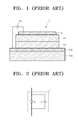
- FIG. 1 is a schematic structural view of a conventional organic light emitting device 1.
- FIG. 2 is an equivalent circuit diagram of the conventional organic light emitting device 1.
- the organic light emitting device 1 is formed by sequentially stacking a transparent electrode 102 which is formed on a glass substrate 105 and operates as anode, an organic transport layer 104 and an organic phosphor layer 103, both of which include organic compounds, and a metal electrode 101 which operates as a cathode.
- a voltage from a driving source 106 is applied between the metal electrode 101 and the transparent electrode 102. Electrons generated by the metal electrode 101 and holes generated by the transparent electrode 102 are recombined to generate excitons. When the excitons are discharged, light is concurrently emitted. The light is emitted through the transparent electrode 102 and the glass substrate 105 to the outside of the organic light emitting device 1. Since the organic light emitting device 1 is formed by stacking an organic phosphor layer (or the like) between electrodes, an equivalent circuit of the organic light emitting device 1 has a parasitic capacitance. That is, as illustrated in FIG. 2, the equivalent circuit diagram of the organic light emitting device 1 includes a luminous body (or a light emitting element) D and a parasitic capacitance C connected in parallel with each other.
- FIG. 3 is a schematic circuit diagram of a conventional organic light emitting display device.
- the conventional organic light emitting display device includes an organic light emitting display panel 2 including a plurality of organic light emitting devices 1, a controller 21, a scan drive source 6, and a data driving source 5.
- data lines D1, D2, ..., Dm and scan lines S1, S2, ..., Sn are formed to cross each other at intervals (which may be predetermined), and organic light emitting devices 1 are formed at the crossing areas of the data lines D1, D2, ..., Dm and the scan lines S1, S2, ..., Sn.
- the controller 21 processes externally inputted image signals SIM.
- Data control signals SDA are applied to the data driving source 5, and scan control signals SSC are applied to the scan drive source 6.
- the data control signals SDA include a data signal.
- the scan control signals SSC include switching control signals for generating a scan signal.
- the data driving source 5 is electrically connected to the data lines D1, D2, ..., Dm and generates a driving current corresponding to the data signal provided by the controller 21 according to the data control signals SDA. Then, the driving current is applied to the data lines D1, D2, ..., Dm.
- the scan drive source 6 is electrically connected to the scan lines S1, S2, ..., Sn and applies a scan signal to the scan lines S1, S2, ..., Sn according to the switching control signals.
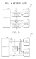
- FIG. 4 is a block diagram illustrating a conventional dual-module organic light emitting display device 400.
- the conventional dual-module organic light emitting display device 400 includes a first module 401, a second module 403, a first power supplier (or power supply) 405, a second power supplier 407, and a controller 409.
- a dual-module organic light emitting display device 400 may be used e.g. in a foldable mobile telephone in order to provide visual feedback both on the outside and the inside of the foldable mobile telephone.
- the first and second modules 401 and 403 each include an organic light emitting display panel 2, a data driving source 5, and a scan drive source 6, each of which was previously described with reference to FIG. 3. Since the conventional organic light emitting display device 400 includes two modules, the conventional organic light emitting display device 400 includes the first power supplier 405 and the second power supplier 407 to provide respective powers to the first module 401 and the second module 403. In addition, the controller 409 applies a control signal SC1 and a data signal DATA1 to the first module 401 and a control signal SC2 and a data signal DATA2 to the second module 403.
- the control signals SC1 and SC2 each include a clock signal, a vertical synchronizing signal, a horizontal synchronization signal, a writing signal, a reading signal, or the like.
- the data signals DATA1 and DATA2 each include a data driving control signal for controlling the operation of the data driving source 5, and a scan driving control signal for controlling the operation of the scan drive source 6.
- Selection signals CS1 and CS2 are signals for respectively selecting the first module 401 and the second module 403 or for selecting both of the first module 401 and the second module 403.
- the first and second power suppliers 405 and 407 are required, the two control signals SC1 and SC2 should be output from the controller 409, and the two data signals DATA1 and DATA2 should be output from the controller 409. Accordingly, the manufacturing costs and the weight of the organic light emitting display device may be increased.
- a first aspect of the present invention provides an inexpensive and light power supply for a dual-module organic light emitting display device.
- the power supply is adapted to selectively supply a first driving voltage to a first module of a dual-module organic light emitting display device or a second driving voltage to a second module of the dual-module organic light emitting display device or to supply the first driving voltage to the first module and to the second module in response to a selection signal provided to the power supply.
- the selection signal of the controller may be adapted to select both the first module and the second module, and the power supply may be adapted to supply a common driving voltage, the common driving voltage being the first driving voltage.
- the power supply may include a voltage divider connected to an output of the power supply, the voltage divider being configured to receive an output voltage of the power supply and adapted to selectively divide the output voltage to generate a feedback voltage.
- the power supply may further include a DC/DC converter connected to the voltage divider and adapted to receive the feedback voltage and to output a voltage at a level corresponding to the feedback voltage.
- the voltage divider may include a first resistor having a first end connected to the output of the power supply, a second resistor and a third resistor, each being connected in series to the first resistor at a second end of the first resistor and the third resistor being connected between the first resistor and a ground terminal.
- the voltage divider may further include a first switch connected between the second resistor and the ground terminal and adapted to be turned on in response to the selection signal.
- the first driving voltage When the first switched is turned on, the first driving voltage may be output from the power supply and may be applied to the first module, and, when the first switch is turned off, the second driving voltage may be output from the power supply and may be applied to the second module.
- the first switch When the selection signal applied from the controller selects both the first module and the second module, the first switch may be turned on and the first driving voltage output from the power supply may be applied to the first module and the second module.
- the power supply may further include a first capacitor connected between an input of the power supply and the ground terminal, the first capacitor being adapted to smooth the input voltage.
- the power supply may further include a second capacitor a second capacitor connected between the output of the power supply and the ground terminal, the second capacitor being adapted to smooth the output voltage.
- the first driving voltage and the second driving voltage may be transmitted through a common power line.
- a second aspect of the present invention provides an organic light emitting display device.
- the organic light emitting display device comprises a first module and a second module, each comprising an organic light emitting display panel and a driving source.
- the organice light emitting display device further includes a controller adapted to apply a common control signal and a data signal to the first module and the second module and to provide a selection signal for selecting at least one of the first module or the second module and a power supply according to the first aspect of the invention.
- a third aspect of the invention provides a foldable mobile telephone comprising an organic light emitting display device according to the second aspect of the invention.
- FIG. 1 is a schematic structural view of a conventional organic light emitting device
- FIG. 2 is an equivalent circuit diagram of the conventional organic light emitting device
- FIG. 3 is a schematic circuit diagram of a conventional organic light emitting display device
- FIG. 4 is a block diagram illustrating a conventional dual-module organic light emitting display device
- FIG. 5 is a block diagram illustrating an organic light emitting display device according to an embodiment of the present invention.
- FIG. 6 is a circuit diagram of a power supply, according to an embodiment of the present invention.
- FIG. 5 is a block diagram illustrating an organic light emitting display device 500 according to an embodiment of the present invention.
- the organic light emitting display device 500 includes a first module 501, a second module 503, a power supplier (or power supply) 505, and a controller 509.
- the first and second modules 501 and 503 each include an organic light emitting display panel 2, a data driving source 5, and a scan drive source 6, each of which was previously described with reference to FIG. 3. Since the conventional organic light emitting display device 400 includes two modules, the organic light emitting display device 400 includes a first power supply (or power supplier) 405 and a second power supply 407 for supplying respective powers to the first module 401 and the second module 403 (see, for example, FIG. 4). However, the organic light emitting display device 500 includes a single power supply 505 rather than two individual power supplies, and thus manufacturing costs may be reduced and the organic light emitting display device 500 may be lighter in weight.
- the power supply 505 supplies an output voltage to the first module 501 and the second module 503.
- the output voltage may be of a first voltage level or a second voltage level, as appropriate for driving the first module 501 or the second module 503, respectively. That is, the power supply 505 effectively generates two driving voltages.
- the power supply 505 will be described in more detail with reference to FIG. 6.
- the controller 509 applies a common control signal SC and a common data signal DATA to the first module 501 and the second module 503.
- the controller 509 applies selection signals CS1 and CS2 for selecting the first module 501 and the second module 503, respectively, or for concurrently selecting both the first module 501 and the second module 503, to the first module 501 and the second module 503, respectively.
- the control signal SC includes a clock signal, vertical synchronizing signal, horizontal synchronization signal, writing signal, reading signal, or the like.
- the data signal DATA includes a data driving control signal for controlling the operation of the data driving source 5 and a scan driving control signal for controlling the operation of the scan drive source 6.
- the selection signals CS1 and CS2 are signals for selecting the first module 501 and the second module 503, respectively, or for selecting both the first module 501 and the second module 503.
- the power supply 505 outputs a first driving voltage.
- the selection signal CS2 selects the second module 503, the power supply 505 outputs a second driving voltage.
- the power supply 505 may supply the first driving voltage (as a common driving voltage).
- the first driving voltage and the second driving voltage which are selectively output from the power supply 505 respectively to the first module 501 and the second module 503, may be applied through a common power line.
- the control signal SC and the data signal DATA are applied to the first module 501 and the second module 503.
- the control signal SC and the data signal DATA may be applied through a common control line and a common data line, respectively.
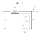
- FIG. 6 is a circuit diagram of the power supply 505, according to an embodiment of the present invention.
- the power supply 505 includes a first capacitor C1, a voltage divider 602, a DC/DC converter 604, and a second capacitor C2.
- the first capacitor C1 is for smoothing (or filtering) an input voltage Vin.
- the smoothed input voltage Vin is output as an output voltage Vout through the DC/DC converter 604 which may include an inductor L, which is a current storage device, and a diode.
- the output voltage Vout is a voltage which is smoothed by the second capacitor C2 and then output from the power supply 505.
- the voltage divider 602 selectively divides the output voltage Vout, which is generated by the DC/DC converter 604, according to the control signal SC.
- the voltage divider 602 includes a first resistance (or resistor) R1, a second resistance R2 and a third resistance R3, each of which is connected in series to the first resistance R1, and a first switch S1 arranged between the second resistance R2 and ground.
- One end of the third resistance R3 is connected to ground.
- the first switch S1 is turned on to connect the second resistance R2 and ground, thereby connecting the second resistance R2 and the third resistance R3 in parallel with each other.
- a divided voltage (Vout/[1+R1/(R2//R3)]) due to a resulting parallel connection of the second resistance R2 and the third resistance R3 is transmitted to a DC/DC converter 604 upon feedback.
- the DC/DC converter 604 converts a voltage level Vin at its input to the output voltage Vout according to the divided voltage (Vout/[1+R1/(R2//R3)]) present at a control input of the DC/DC converter 604.
- the second resistance R2 is not connected in parallel to the third resistance R3 any more.
- the divided voltage (Vout/[1+R1/R3]) is transmitted to the control input of the DC/DC converter 604 upon feedback.
- the DC/DC converter 604 converts a voltage level Vin at its input to the output voltage Vout according to the divided voltage (Vout/[1+R1/R3]) present at the control input of DC/DC converter 604.
- a first driving voltage is a voltage output from the power supply 505 in order to drive the first module 501.
- a second driving voltage is a voltage output from the power supply 505 in order to drive the second module 503.
- the first module 501 may be a main module, and the second module 503 may be a sub module.
- the first driving voltage of the first module 501 may be about 18 V
- the second driving voltage of the second module 503 may be about 14 V.
- both of the selection signals CS1 and CS2 are applied to the first module 501 and the second module 503, respectively.
- the power supply 505 concurrently supplies the first driving voltage higher than the second driving voltage to the first module 501 and the second module 503. This is because when the power supply 505 supplies the second driving voltage lower than the first driving voltage to the first module 501 and the second module 503, the first module 501 may not operate normally.
- the first driving voltage and the second driving voltage which is output from the power supply 505 to the first module 501 and the second module 503, respectively, may be transmitted through a common power line.
- the present invention has the following features.
- the power supply supplies two different driving voltages, and thus the manufacturing costs and the weight of the organic light emitting display device can be decreased.
- the manufacturing costs of the organic light emitting display device can be decreased.
Landscapes
- Engineering & Computer Science (AREA)
- Physics & Mathematics (AREA)
- Computer Hardware Design (AREA)
- General Physics & Mathematics (AREA)
- Theoretical Computer Science (AREA)
- Control Of El Displays (AREA)
- Electroluminescent Light Sources (AREA)
- Control Of Indicators Other Than Cathode Ray Tubes (AREA)
Abstract
Description
- The present invention relates to an organic light emitting display device and a power supply for the same.
- Recently, self-emitting light display devices have received considerable attention. In particular, organic light emitting display devices have attracted much attention. The organic light emitting display devices include pixels corresponding to organic light emitting devices which emit light when an electric field is applied thereto.
- FIG. 1 is a schematic structural view of a conventional organic
light emitting device 1. FIG. 2 is an equivalent circuit diagram of the conventional organiclight emitting device 1. - Referring to FIGS. 1 and 2, the organic
light emitting device 1 is formed by sequentially stacking atransparent electrode 102 which is formed on aglass substrate 105 and operates as anode, anorganic transport layer 104 and anorganic phosphor layer 103, both of which include organic compounds, and ametal electrode 101 which operates as a cathode. - A voltage from a
driving source 106 is applied between themetal electrode 101 and thetransparent electrode 102. Electrons generated by themetal electrode 101 and holes generated by thetransparent electrode 102 are recombined to generate excitons. When the excitons are discharged, light is concurrently emitted. The light is emitted through thetransparent electrode 102 and theglass substrate 105 to the outside of the organiclight emitting device 1. Since the organiclight emitting device 1 is formed by stacking an organic phosphor layer (or the like) between electrodes, an equivalent circuit of the organiclight emitting device 1 has a parasitic capacitance. That is, as illustrated in FIG. 2, the equivalent circuit diagram of the organiclight emitting device 1 includes a luminous body (or a light emitting element) D and a parasitic capacitance C connected in parallel with each other. - FIG. 3 is a schematic circuit diagram of a conventional organic light emitting display device.
- Referring to FIG. 3, the conventional organic light emitting display device includes an organic light
emitting display panel 2 including a plurality of organiclight emitting devices 1, acontroller 21, ascan drive source 6, and adata driving source 5. - In the organic light
emitting display panel 2, data lines D1, D2, ..., Dm and scan lines S1, S2, ..., Sn are formed to cross each other at intervals (which may be predetermined), and organiclight emitting devices 1 are formed at the crossing areas of the data lines D1, D2, ..., Dm and the scan lines S1, S2, ..., Sn. - The
controller 21 processes externally inputted image signals SIM. Data control signals SDA are applied to thedata driving source 5, and scan control signals SSC are applied to thescan drive source 6. The data control signals SDA include a data signal. The scan control signals SSC include switching control signals for generating a scan signal. Thedata driving source 5 is electrically connected to the data lines D1, D2, ..., Dm and generates a driving current corresponding to the data signal provided by thecontroller 21 according to the data control signals SDA. Then, the driving current is applied to the data lines D1, D2, ..., Dm. - The
scan drive source 6 is electrically connected to the scan lines S1, S2, ..., Sn and applies a scan signal to the scan lines S1, S2, ..., Sn according to the switching control signals. - FIG. 4 is a block diagram illustrating a conventional dual-module organic light
emitting display device 400. - Referring to FIG. 4, the conventional dual-module organic light
emitting display device 400 includes afirst module 401, asecond module 403, a first power supplier (or power supply) 405, asecond power supplier 407, and acontroller 409. Such a dual-module organic lightemitting display device 400 may be used e.g. in a foldable mobile telephone in order to provide visual feedback both on the outside and the inside of the foldable mobile telephone. - The first and
second modules emitting display panel 2, adata driving source 5, and ascan drive source 6, each of which was previously described with reference to FIG. 3. Since the conventional organic lightemitting display device 400 includes two modules, the conventional organic lightemitting display device 400 includes thefirst power supplier 405 and thesecond power supplier 407 to provide respective powers to thefirst module 401 and thesecond module 403. In addition, thecontroller 409 applies a control signal SC1 and a data signal DATA1 to thefirst module 401 and a control signal SC2 and a data signal DATA2 to thesecond module 403. The control signals SC1 and SC2 each include a clock signal, a vertical synchronizing signal, a horizontal synchronization signal, a writing signal, a reading signal, or the like. The data signals DATA1 and DATA2 each include a data driving control signal for controlling the operation of thedata driving source 5, and a scan driving control signal for controlling the operation of thescan drive source 6. Selection signals CS1 and CS2 are signals for respectively selecting thefirst module 401 and thesecond module 403 or for selecting both of thefirst module 401 and thesecond module 403. - According to the dual-module conventional organic light
emitting display device 400, the first andsecond power suppliers controller 409, and the two data signals DATA1 and DATA2 should be output from thecontroller 409. Accordingly, the manufacturing costs and the weight of the organic light emitting display device may be increased. - A first aspect of the present invention provides an inexpensive and light power supply for a dual-module organic light emitting display device.
- The power supply is adapted to selectively supply a first driving voltage to a first module of a dual-module organic light emitting display device or a second driving voltage to a second module of the dual-module organic light emitting display device or to supply the first driving voltage to the first module and to the second module in response to a selection signal provided to the power supply.
- The selection signal of the controller may be adapted to select both the first module and the second module, and the power supply may be adapted to supply a common driving voltage, the common driving voltage being the first driving voltage.
- The power supply may include a voltage divider connected to an output of the power supply, the voltage divider being configured to receive an output voltage of the power supply and adapted to selectively divide the output voltage to generate a feedback voltage. The power supply may further include a DC/DC converter connected to the voltage divider and adapted to receive the feedback voltage and to output a voltage at a level corresponding to the feedback voltage.
- The voltage divider may include a first resistor having a first end connected to the output of the power supply, a second resistor and a third resistor, each being connected in series to the first resistor at a second end of the first resistor and the third resistor being connected between the first resistor and a ground terminal. The voltage divider may further include a first switch connected between the second resistor and the ground terminal and adapted to be turned on in response to the selection signal.
- When the first switched is turned on, the first driving voltage may be output from the power supply and may be applied to the first module, and, when the first switch is turned off, the second driving voltage may be output from the power supply and may be applied to the second module.
- When the selection signal applied from the controller selects both the first module and the second module, the first switch may be turned on and the first driving voltage output from the power supply may be applied to the first module and the second module.
- The power supply may further include a first capacitor connected between an input of the power supply and the ground terminal, the first capacitor being adapted to smooth the input voltage.
- The power supply may further include a second capacitor a second capacitor connected between the output of the power supply and the ground terminal, the second capacitor being adapted to smooth the output voltage.
- The first driving voltage and the second driving voltage may be transmitted through a common power line.
- A second aspect of the present invention provides an organic light emitting display device. The organic light emitting display device comprises a first module and a second module, each comprising an organic light emitting display panel and a driving source. The organice light emitting display device further includes a controller adapted to apply a common control signal and a data signal to the first module and the second module and to provide a selection signal for selecting at least one of the first module or the second module and a power supply according to the first aspect of the invention. A third aspect of the invention provides a foldable mobile telephone comprising an organic light emitting display device according to the second aspect of the invention.
- The above and other features and aspects of the present invention will become more apparent by describing in detail exemplary embodiments thereof with reference to the attached drawings in which:
- FIG. 1 is a schematic structural view of a conventional organic light emitting device;
- FIG. 2 is an equivalent circuit diagram of the conventional organic light emitting device;
- FIG. 3 is a schematic circuit diagram of a conventional organic light emitting display device;
- FIG. 4 is a block diagram illustrating a conventional dual-module organic light emitting display device;
- FIG. 5 is a block diagram illustrating an organic light emitting display device according to an embodiment of the present invention; and
- FIG. 6 is a circuit diagram of a power supply, according to an embodiment of the present invention.
- The present invention will now be described more fully with reference to the accompanying drawings, in which exemplary embodiments of the invention are shown.
- FIG. 5 is a block diagram illustrating an organic light emitting
display device 500 according to an embodiment of the present invention. - Referring to FIG. 5, the organic light emitting
display device 500 includes afirst module 501, asecond module 503, a power supplier (or power supply) 505, and acontroller 509. - The first and
second modules display panel 2, adata driving source 5, and ascan drive source 6, each of which was previously described with reference to FIG. 3. Since the conventional organic light emittingdisplay device 400 includes two modules, the organic light emittingdisplay device 400 includes a first power supply (or power supplier) 405 and asecond power supply 407 for supplying respective powers to thefirst module 401 and the second module 403 (see, for example, FIG. 4). However, the organic light emittingdisplay device 500 includes asingle power supply 505 rather than two individual power supplies, and thus manufacturing costs may be reduced and the organic light emittingdisplay device 500 may be lighter in weight. - The
power supply 505 supplies an output voltage to thefirst module 501 and thesecond module 503. The output voltage may be of a first voltage level or a second voltage level, as appropriate for driving thefirst module 501 or thesecond module 503, respectively. That is, thepower supply 505 effectively generates two driving voltages. Thepower supply 505 will be described in more detail with reference to FIG. 6. - The
controller 509 applies a common control signal SC and a common data signal DATA to thefirst module 501 and thesecond module 503. In addition, thecontroller 509 applies selection signals CS1 and CS2 for selecting thefirst module 501 and thesecond module 503, respectively, or for concurrently selecting both thefirst module 501 and thesecond module 503, to thefirst module 501 and thesecond module 503, respectively. The control signal SC includes a clock signal, vertical synchronizing signal, horizontal synchronization signal, writing signal, reading signal, or the like. The data signal DATA includes a data driving control signal for controlling the operation of thedata driving source 5 and a scan driving control signal for controlling the operation of thescan drive source 6. The selection signals CS1 and CS2 are signals for selecting thefirst module 501 and thesecond module 503, respectively, or for selecting both thefirst module 501 and thesecond module 503. When the selection signal CS1 selects thefirst module 501, thepower supply 505 outputs a first driving voltage. When the selection signal CS2 selects thesecond module 503, thepower supply 505 outputs a second driving voltage. When the selection signals CS1 and CS2 concurrently select both thefirst module 501 and thesecond module 503, thepower supply 505 may supply the first driving voltage (as a common driving voltage). - In the organic light emitting
display device 500, the first driving voltage and the second driving voltage, which are selectively output from thepower supply 505 respectively to thefirst module 501 and thesecond module 503, may be applied through a common power line. The control signal SC and the data signal DATA are applied to thefirst module 501 and thesecond module 503. The control signal SC and the data signal DATA may be applied through a common control line and a common data line, respectively. - FIG. 6 is a circuit diagram of the
power supply 505, according to an embodiment of the present invention. - Referring to FIG. 6, the
power supply 505 includes a first capacitor C1, avoltage divider 602, a DC/DC converter 604, and a second capacitor C2. - The first capacitor C1 is for smoothing (or filtering) an input voltage Vin. The smoothed input voltage Vin is output as an output voltage Vout through the DC/
DC converter 604 which may include an inductor L, which is a current storage device, and a diode. The output voltage Vout is a voltage which is smoothed by the second capacitor C2 and then output from thepower supply 505. - The
voltage divider 602 selectively divides the output voltage Vout, which is generated by the DC/DC converter 604, according to the control signal SC. To achieve this, thevoltage divider 602 includes a first resistance (or resistor) R1, a second resistance R2 and a third resistance R3, each of which is connected in series to the first resistance R1, and a first switch S1 arranged between the second resistance R2 and ground. One end of the third resistance R3 is connected to ground. The first switch S1 is turned on to connect the second resistance R2 and ground, thereby connecting the second resistance R2 and the third resistance R3 in parallel with each other. - According to the structure of the
voltage divider 602, when the first switch S1 is turned on, that is, when the control signal SC selects thefirst module 501, a divided voltage (Vout/[1+R1/(R2//R3)]) due to a resulting parallel connection of the second resistance R2 and the third resistance R3 is transmitted to a DC/DC converter 604 upon feedback. The DC/DC converter 604 converts a voltage level Vin at its input to the output voltage Vout according to the divided voltage (Vout/[1+R1/(R2//R3)]) present at a control input of the DC/DC converter 604. Due to the feedback structure formed by resistor R1, the DC/DC converter 604, output voltage Vout will rise when a lower voltage is present at input node N1 of the DC/DC converter 604. Thus, by changing the ratio between the output voltage Vout and the voltage present at node N1 the output voltage Vout can be adjusted. - When the first switch S1 is turned off, that is, when the control signal SC selects the
second module 503, the second resistance R2 is not connected in parallel to the third resistance R3 any more. Thus, the divided voltage (Vout/[1+R1/R3]) is transmitted to the control input of the DC/DC converter 604 upon feedback. The DC/DC converter 604 converts a voltage level Vin at its input to the output voltage Vout according to the divided voltage (Vout/[1+R1/R3]) present at the control input of DC/DC converter 604. - When the control signal SC selects the
first module 501, a higher output voltage is output from thepower supply 505 relative to the case where the control signal SC selects thesecond module 503 due to the type of voltage division. A first driving voltage is a voltage output from thepower supply 505 in order to drive thefirst module 501. A second driving voltage is a voltage output from thepower supply 505 in order to drive thesecond module 503. In the organic light emittingdisplay device 500 including two modules, thefirst module 501 may be a main module, and thesecond module 503 may be a sub module. Thus, by way of example, the first driving voltage of thefirst module 501 may be about 18 V, and the second driving voltage of thesecond module 503 may be about 14 V. - When the control signal SC selects both of the
first module 501 and thesecond module 503, both of the selection signals CS1 and CS2 are applied to thefirst module 501 and thesecond module 503, respectively. Here, thepower supply 505 concurrently supplies the first driving voltage higher than the second driving voltage to thefirst module 501 and thesecond module 503. This is because when thepower supply 505 supplies the second driving voltage lower than the first driving voltage to thefirst module 501 and thesecond module 503, thefirst module 501 may not operate normally. - The first driving voltage and the second driving voltage, which is output from the
power supply 505 to thefirst module 501 and thesecond module 503, respectively, may be transmitted through a common power line. - The present invention has the following features.
- In the organic light emitting display device using two modules, the power supply supplies two different driving voltages, and thus the manufacturing costs and the weight of the organic light emitting display device can be decreased.
- In addition, since the organic light emitting display device using two modules commonly uses a common power line, a common control line for transferring a control signal, and a common data line for transferring a data signal, the manufacturing costs of the organic light emitting display device can be decreased.
Claims (7)
- A power supply for an organic light emitting display device comprising a first module and a second module, each module comprising an organic light emitting display panel and a driving source, the power supply being adapted to selectively supply a first driving voltage to the first module or a second driving voltage to the second module or to supply the first driving voltage to the first module and to the second module in response to a selection signal provided to the power supply.
- The power supply of claim 1, the power supply comprising:a voltage divider connected to an output of the power supply, the voltage divider being configured to receive an output voltage of the power supply and adapted to selectively divide the output voltage to generate a feedback voltage; anda DC/DC converter connected to the voltage divider and adapted to receive the feedback voltage and to output a voltage at a level corresponding to the feedback voltage.
- The power supply of claim 2, wherein the voltage divider comprises:a first resistor having a first end connected to the output of the power supply;a second resistor and a third resistor, each being connected in series to the first resistor at a second end of the first resistor and the third resistor being connected between the first resistor and a ground terminal; anda first switch connected between the second resistor and the ground terminal and adapted to be turned on in response to the selection signal.
- The power supply of claim 3, further comprising a first capacitor connected between an input of the power supply and the ground terminal, the first capacitor being adapted to smooth the input voltage.
- The power supply of one of claims 3 or 4, further comprising a second capacitor connected between the output of the power supply and the ground terminal, the second capacitor being adapted to smooth the output voltage.
- An organic light emitting display device comprising:a first module and a second module, each comprising an organic light emitting display panel and a driving source;a controller adapted to apply a common control signal and a data signal to the first module and the second module and to provide a selection signal; anda power supply according to one of the preceding claims, the power supply being connected to the controller, the first module, and the second module and adapted to selectively supply a first driving voltage to the first module or a second driving voltage to the second module or to supply the first driving voltage to the first module and to the second module in response to the selection signal.
- A foldable mobile telephone comprising an organic light emitting display device according to claim 6.
Applications Claiming Priority (1)
| Application Number | Priority Date | Filing Date | Title |
|---|---|---|---|
| KR1020060043950A KR100795797B1 (en) | 2006-05-16 | 2006-05-16 | Organic light emitting display device and power supply unit of organic light emitting display device |
Publications (1)
| Publication Number | Publication Date |
|---|---|
| EP1857999A1 true EP1857999A1 (en) | 2007-11-21 |
Family
ID=38320301
Family Applications (1)
| Application Number | Title | Priority Date | Filing Date |
|---|---|---|---|
| EP07108341A Ceased EP1857999A1 (en) | 2006-05-16 | 2007-05-16 | Organic light emitting display device and power supply unit for the same |
Country Status (6)
| Country | Link |
|---|---|
| US (1) | US8379008B2 (en) |
| EP (1) | EP1857999A1 (en) |
| JP (1) | JP5318363B2 (en) |
| KR (1) | KR100795797B1 (en) |
| CN (1) | CN101075408A (en) |
| TW (1) | TWI378427B (en) |
Cited By (1)
| Publication number | Priority date | Publication date | Assignee | Title |
|---|---|---|---|---|
| EP2056282A3 (en) * | 2007-10-29 | 2010-08-11 | Samsung Mobile Display Co., Ltd. | Organic light emitting display and power supply method thereof |
Families Citing this family (6)
| Publication number | Priority date | Publication date | Assignee | Title |
|---|---|---|---|---|
| CN101546204B (en) * | 2008-03-25 | 2011-02-02 | 联咏科技股份有限公司 | Voltage generator with dynamic resistance feedback control |
| KR101346858B1 (en) * | 2008-11-12 | 2014-01-02 | 엘지디스플레이 주식회사 | Organic electro-luminescence display device |
| KR20160016413A (en) * | 2014-08-05 | 2016-02-15 | 삼성전자주식회사 | Display system and control method of the same |
| KR102518745B1 (en) * | 2015-10-13 | 2023-04-07 | 삼성디스플레이 주식회사 | Display Device and Driving Method Thereof |
| CN106383611B (en) * | 2016-09-27 | 2019-03-12 | 京东方科技集团股份有限公司 | Display control circuit, display control method, and display device |
| US11605968B2 (en) * | 2021-03-29 | 2023-03-14 | Pliops Ltd. | Charging device for charging a supercapacitor |
Citations (5)
| Publication number | Priority date | Publication date | Assignee | Title |
|---|---|---|---|---|
| US20040252096A1 (en) | 2003-05-21 | 2004-12-16 | Der-Jiunn Wang | Dual panel display backlight power controller chip for handheld apparatus |
| EP1542066A1 (en) | 2002-09-20 | 2005-06-15 | Matsushita Electric Industrial Co., Ltd. | Liquid crystal display device, and portable telephone device using liquid crystal display device |
| US20050143137A1 (en) | 2003-12-25 | 2005-06-30 | Fujitsu Limited | Terminal apparatus |
| US20050253773A1 (en) | 2002-09-25 | 2005-11-17 | Kanetaka Sekiguchi | Display |
| EP1619653A2 (en) | 2004-07-20 | 2006-01-25 | LG Electronics, Inc. | Multi-panel display device and method of driving the same |
Family Cites Families (24)
| Publication number | Priority date | Publication date | Assignee | Title |
|---|---|---|---|---|
| US5841431A (en) | 1996-11-15 | 1998-11-24 | Intel Corporation | Application of split- and dual-screen LCD panel design in cellular phones |
| KR100257714B1 (en) * | 1997-11-06 | 2000-06-01 | 손욱 | Foldable Flat Panel Display Drives |
| JPH11327511A (en) * | 1998-05-07 | 1999-11-26 | Hitachi Ltd | LCD display control circuit |
| KR100348275B1 (en) | 2000-07-28 | 2002-08-09 | 엘지전자 주식회사 | driving control circuit in organic electroluminescence |
| KR100709717B1 (en) * | 2001-03-07 | 2007-04-19 | 삼성전자주식회사 | Liquid Crystal Display with Multiple Screens |
| JP3623752B2 (en) | 2001-04-23 | 2005-02-23 | 埼玉日本電気株式会社 | Folding mobile phone |
| JP2004109595A (en) | 2002-09-19 | 2004-04-08 | Melco Display Technology Kk | Display device and its driving method |
| JP4794801B2 (en) | 2002-10-03 | 2011-10-19 | ルネサスエレクトロニクス株式会社 | Display device for portable electronic device |
| JP4552437B2 (en) * | 2003-03-20 | 2010-09-29 | マグナチップセミコンダクター有限会社 | Display device |
| TWI220751B (en) * | 2003-05-06 | 2004-09-01 | Toppoly Optoelectronics Corp | Driving circuit for double display pannel |
| US7385598B2 (en) * | 2003-06-27 | 2008-06-10 | Samsung Electronics, Co., Ltd. | Driver for operating multiple display devices |
| JP4485184B2 (en) | 2003-12-15 | 2010-06-16 | 株式会社半導体エネルギー研究所 | LIGHT EMITTING DEVICE AND ELECTRONIC DEVICE |
| JP5124137B2 (en) * | 2004-03-10 | 2013-01-23 | ローム株式会社 | Organic EL display device |
| JP4499472B2 (en) | 2004-04-28 | 2010-07-07 | オプトレックス株式会社 | Drive device for organic EL display device |
| JP2005332914A (en) | 2004-05-19 | 2005-12-02 | Mitsubishi Materials Corp | Radio wave absorber with excellent flame resistance |
| JP4939770B2 (en) | 2004-05-21 | 2012-05-30 | 株式会社半導体エネルギー研究所 | Display device |
| US8681140B2 (en) * | 2004-05-21 | 2014-03-25 | Semiconductor Energy Laboratory Co., Ltd. | Display device and electronic apparatus having the same |
| JP4047839B2 (en) * | 2004-08-09 | 2008-02-13 | 株式会社東芝 | Display device and portable electronic device |
| KR100570772B1 (en) * | 2004-08-20 | 2006-04-12 | 삼성에스디아이 주식회사 | Display panel driving driver and method of light emitting display device |
| KR20060025784A (en) * | 2004-09-17 | 2006-03-22 | 삼성전자주식회사 | Display device |
| JP5062990B2 (en) * | 2004-11-19 | 2012-10-31 | 株式会社半導体エネルギー研究所 | Display device |
| KR20060085289A (en) | 2005-01-21 | 2006-07-26 | 삼성전자주식회사 | Dual display |
| TWI408542B (en) * | 2005-05-12 | 2013-09-11 | 樂金顯示科技股份有限公司 | Equipment for supplying power |
| KR100669205B1 (en) * | 2005-06-17 | 2007-01-16 | 엘지전자 주식회사 | Drive of dual flat panel display |
-
2006
- 2006-05-16 KR KR1020060043950A patent/KR100795797B1/en not_active Expired - Fee Related
-
2007
- 2007-04-19 US US11/737,646 patent/US8379008B2/en not_active Expired - Fee Related
- 2007-04-20 JP JP2007111396A patent/JP5318363B2/en not_active Expired - Fee Related
- 2007-05-14 TW TW096117050A patent/TWI378427B/en not_active IP Right Cessation
- 2007-05-16 EP EP07108341A patent/EP1857999A1/en not_active Ceased
- 2007-05-16 CN CNA2007101038434A patent/CN101075408A/en active Pending
Patent Citations (5)
| Publication number | Priority date | Publication date | Assignee | Title |
|---|---|---|---|---|
| EP1542066A1 (en) | 2002-09-20 | 2005-06-15 | Matsushita Electric Industrial Co., Ltd. | Liquid crystal display device, and portable telephone device using liquid crystal display device |
| US20050253773A1 (en) | 2002-09-25 | 2005-11-17 | Kanetaka Sekiguchi | Display |
| US20040252096A1 (en) | 2003-05-21 | 2004-12-16 | Der-Jiunn Wang | Dual panel display backlight power controller chip for handheld apparatus |
| US20050143137A1 (en) | 2003-12-25 | 2005-06-30 | Fujitsu Limited | Terminal apparatus |
| EP1619653A2 (en) | 2004-07-20 | 2006-01-25 | LG Electronics, Inc. | Multi-panel display device and method of driving the same |
Non-Patent Citations (2)
| Title |
|---|
| "269 Cs", 1983, ELEKTOR-VERLAG, pages: 62 |
| "269 ICs", 1983, ELEKTOR-VERLAG, AACHEN * |
Cited By (2)
| Publication number | Priority date | Publication date | Assignee | Title |
|---|---|---|---|---|
| EP2056282A3 (en) * | 2007-10-29 | 2010-08-11 | Samsung Mobile Display Co., Ltd. | Organic light emitting display and power supply method thereof |
| US9041626B2 (en) | 2007-10-29 | 2015-05-26 | Samsung Display Co., Ltd. | Organic light emitting display and power supply method thereof |
Also Published As
| Publication number | Publication date |
|---|---|
| KR20070111075A (en) | 2007-11-21 |
| JP5318363B2 (en) | 2013-10-16 |
| TW200744055A (en) | 2007-12-01 |
| KR100795797B1 (en) | 2008-01-21 |
| US20070269168A1 (en) | 2007-11-22 |
| US8379008B2 (en) | 2013-02-19 |
| CN101075408A (en) | 2007-11-21 |
| JP2007310381A (en) | 2007-11-29 |
| TWI378427B (en) | 2012-12-01 |
Similar Documents
| Publication | Publication Date | Title |
|---|---|---|
| EP1978504B1 (en) | Organic light emitting diode (OLED) display and a method of driving the same | |
| KR100602065B1 (en) | Power supply device and its driving method and driving device and driving method of electroluminescence display device using the same | |
| US9535440B2 (en) | DC-DC converter and organic light emitting display device using the same | |
| US9123286B2 (en) | Power generator having a power selector and organic light emitting display device using the same | |
| KR101903703B1 (en) | DC-DC Converter and Organic Light Emitting Display including The Same | |
| KR102057286B1 (en) | Organic Light Emitting Display | |
| US8519914B2 (en) | Organic light emitting display device | |
| US8379008B2 (en) | Organic light emitting display device and power supply unit for the same | |
| US8581897B2 (en) | DC-DC converter and organic light emitting display using the same | |
| KR102085061B1 (en) | DC-DC Converter and Organic Light Emitting Display including The Same | |
| US7236148B2 (en) | Drive method of light-emitting display panel and organic EL display device | |
| CN102834858A (en) | Organic el display device | |
| KR20130072175A (en) | Backlight module and driving method thereof and display device using the same | |
| EP1876582A2 (en) | Organic light emitting display and driving method thereof | |
| US9414461B2 (en) | DC-DC converter and organic light emitting display device including the same | |
| EP2475083A2 (en) | DC-DC converter and mobile communication terminal using the same | |
| KR101633426B1 (en) | Power supplying apparatus of Organic Light Emitting Display | |
| US9443468B2 (en) | Display device and controller therefor | |
| EP2690772A2 (en) | Voltage generator, driving method for the voltage generator, and organic light emitting display device using the same | |
| EP2298031A2 (en) | Organic light emitting diode driver arrangement | |
| US20250008623A1 (en) | Two-stage power supply architecture with flyback/llc and buck converter for led display | |
| KR101554583B1 (en) | Organic electroluminescent display and method of driving the same | |
| US20140118323A1 (en) | Organic light emitting display | |
| KR20080068428A (en) | Organic light emitting display device | |
| KR102606744B1 (en) | DC Power supply for driving display panel |
Legal Events
| Date | Code | Title | Description |
|---|---|---|---|
| PUAI | Public reference made under article 153(3) epc to a published international application that has entered the european phase |
Free format text: ORIGINAL CODE: 0009012 |
|
| 17P | Request for examination filed |
Effective date: 20070516 |
|
| AK | Designated contracting states |
Kind code of ref document: A1 Designated state(s): AT BE BG CH CY CZ DE DK EE ES FI FR GB GR HU IE IS IT LI LT LU LV MC MT NL PL PT RO SE SI SK TR |
|
| AX | Request for extension of the european patent |
Extension state: AL BA HR MK YU |
|
| RIN1 | Information on inventor provided before grant (corrected) |
Inventor name: KIM, SANG-WOOK Inventor name: PARK, JUNG-KOOK |
|
| AKX | Designation fees paid |
Designated state(s): DE FR GB HU |
|
| 17Q | First examination report despatched |
Effective date: 20080808 |
|
| RAP1 | Party data changed (applicant data changed or rights of an application transferred) |
Owner name: SAMSUNG MOBILE DISPLAY CO., LTD. |
|
| STAA | Information on the status of an ep patent application or granted ep patent |
Free format text: STATUS: THE APPLICATION HAS BEEN REFUSED |
|
| 18R | Application refused |
Effective date: 20090511 |