EP2475083A2 - DC-DC converter and mobile communication terminal using the same - Google Patents
DC-DC converter and mobile communication terminal using the same Download PDFInfo
- Publication number
- EP2475083A2 EP2475083A2 EP11190064A EP11190064A EP2475083A2 EP 2475083 A2 EP2475083 A2 EP 2475083A2 EP 11190064 A EP11190064 A EP 11190064A EP 11190064 A EP11190064 A EP 11190064A EP 2475083 A2 EP2475083 A2 EP 2475083A2
- Authority
- EP
- European Patent Office
- Prior art keywords
- voltage
- converter
- input voltage
- output terminal
- resistor
- Prior art date
- Legal status (The legal status is an assumption and is not a legal conclusion. Google has not performed a legal analysis and makes no representation as to the accuracy of the status listed.)
- Withdrawn
Links
Images

Classifications
-
- H—ELECTRICITY
- H02—GENERATION; CONVERSION OR DISTRIBUTION OF ELECTRIC POWER
- H02M—APPARATUS FOR CONVERSION BETWEEN AC AND AC, BETWEEN AC AND DC, OR BETWEEN DC AND DC, AND FOR USE WITH MAINS OR SIMILAR POWER SUPPLY SYSTEMS; CONVERSION OF DC OR AC INPUT POWER INTO SURGE OUTPUT POWER; CONTROL OR REGULATION THEREOF
- H02M3/00—Conversion of dc power input into dc power output
-
- F—MECHANICAL ENGINEERING; LIGHTING; HEATING; WEAPONS; BLASTING
- F24—HEATING; RANGES; VENTILATING
- F24D—DOMESTIC- OR SPACE-HEATING SYSTEMS, e.g. CENTRAL HEATING SYSTEMS; DOMESTIC HOT-WATER SUPPLY SYSTEMS; ELEMENTS OR COMPONENTS THEREFOR
- F24D3/00—Hot-water central heating systems
- F24D3/12—Tube and panel arrangements for ceiling, wall, or underfloor heating
- F24D3/14—Tube and panel arrangements for ceiling, wall, or underfloor heating incorporated in a ceiling, wall or floor
- F24D3/141—Tube mountings specially adapted therefor
- F24D3/143—Tube clips with barbed anchors
-
- E—FIXED CONSTRUCTIONS
- E04—BUILDING
- E04C—STRUCTURAL ELEMENTS; BUILDING MATERIALS
- E04C2/00—Building elements of relatively thin form for the construction of parts of buildings, e.g. sheet materials, slabs, or panels
- E04C2/44—Building elements of relatively thin form for the construction of parts of buildings, e.g. sheet materials, slabs, or panels characterised by the purpose
- E04C2/52—Building elements of relatively thin form for the construction of parts of buildings, e.g. sheet materials, slabs, or panels characterised by the purpose with special adaptations for auxiliary purposes, e.g. serving for locating conduits
- E04C2/521—Building elements of relatively thin form for the construction of parts of buildings, e.g. sheet materials, slabs, or panels characterised by the purpose with special adaptations for auxiliary purposes, e.g. serving for locating conduits serving for locating conduits; for ventilating, heating or cooling
- E04C2/525—Building elements of relatively thin form for the construction of parts of buildings, e.g. sheet materials, slabs, or panels characterised by the purpose with special adaptations for auxiliary purposes, e.g. serving for locating conduits serving for locating conduits; for ventilating, heating or cooling for heating or cooling
-
- E—FIXED CONSTRUCTIONS
- E04—BUILDING
- E04F—FINISHING WORK ON BUILDINGS, e.g. STAIRS, FLOORS
- E04F2290/00—Specially adapted covering, lining or flooring elements not otherwise provided for
- E04F2290/02—Specially adapted covering, lining or flooring elements not otherwise provided for for accommodating service installations or utility lines, e.g. heating conduits, electrical lines, lighting devices or service outlets
- E04F2290/023—Specially adapted covering, lining or flooring elements not otherwise provided for for accommodating service installations or utility lines, e.g. heating conduits, electrical lines, lighting devices or service outlets for heating
-
- H—ELECTRICITY
- H02—GENERATION; CONVERSION OR DISTRIBUTION OF ELECTRIC POWER
- H02J—CIRCUIT ARRANGEMENTS OR SYSTEMS FOR SUPPLYING OR DISTRIBUTING ELECTRIC POWER; SYSTEMS FOR STORING ELECTRIC ENERGY
- H02J2207/00—Indexing scheme relating to details of circuit arrangements for charging or depolarising batteries or for supplying loads from batteries
- H02J2207/20—Charging or discharging characterised by the power electronics converter
-
- H—ELECTRICITY
- H02—GENERATION; CONVERSION OR DISTRIBUTION OF ELECTRIC POWER
- H02M—APPARATUS FOR CONVERSION BETWEEN AC AND AC, BETWEEN AC AND DC, OR BETWEEN DC AND DC, AND FOR USE WITH MAINS OR SIMILAR POWER SUPPLY SYSTEMS; CONVERSION OF DC OR AC INPUT POWER INTO SURGE OUTPUT POWER; CONTROL OR REGULATION THEREOF
- H02M1/00—Details of apparatus for conversion
- H02M1/0003—Details of control, feedback or regulation circuits
- H02M1/0032—Control circuits allowing low power mode operation, e.g. in standby mode
-
- H—ELECTRICITY
- H02—GENERATION; CONVERSION OR DISTRIBUTION OF ELECTRIC POWER
- H02M—APPARATUS FOR CONVERSION BETWEEN AC AND AC, BETWEEN AC AND DC, OR BETWEEN DC AND DC, AND FOR USE WITH MAINS OR SIMILAR POWER SUPPLY SYSTEMS; CONVERSION OF DC OR AC INPUT POWER INTO SURGE OUTPUT POWER; CONTROL OR REGULATION THEREOF
- H02M1/00—Details of apparatus for conversion
- H02M1/14—Arrangements for reducing ripples from dc input or output
- H02M1/15—Arrangements for reducing ripples from dc input or output using active elements
-
- Y—GENERAL TAGGING OF NEW TECHNOLOGICAL DEVELOPMENTS; GENERAL TAGGING OF CROSS-SECTIONAL TECHNOLOGIES SPANNING OVER SEVERAL SECTIONS OF THE IPC; TECHNICAL SUBJECTS COVERED BY FORMER USPC CROSS-REFERENCE ART COLLECTIONS [XRACs] AND DIGESTS
- Y02—TECHNOLOGIES OR APPLICATIONS FOR MITIGATION OR ADAPTATION AGAINST CLIMATE CHANGE
- Y02B—CLIMATE CHANGE MITIGATION TECHNOLOGIES RELATED TO BUILDINGS, e.g. HOUSING, HOUSE APPLIANCES OR RELATED END-USER APPLICATIONS
- Y02B30/00—Energy efficient heating, ventilation or air conditioning [HVAC]
-
- Y—GENERAL TAGGING OF NEW TECHNOLOGICAL DEVELOPMENTS; GENERAL TAGGING OF CROSS-SECTIONAL TECHNOLOGIES SPANNING OVER SEVERAL SECTIONS OF THE IPC; TECHNICAL SUBJECTS COVERED BY FORMER USPC CROSS-REFERENCE ART COLLECTIONS [XRACs] AND DIGESTS
- Y02—TECHNOLOGIES OR APPLICATIONS FOR MITIGATION OR ADAPTATION AGAINST CLIMATE CHANGE
- Y02B—CLIMATE CHANGE MITIGATION TECHNOLOGIES RELATED TO BUILDINGS, e.g. HOUSING, HOUSE APPLIANCES OR RELATED END-USER APPLICATIONS
- Y02B70/00—Technologies for an efficient end-user side electric power management and consumption
- Y02B70/10—Technologies improving the efficiency by using switched-mode power supplies [SMPS], i.e. efficient power electronics conversion e.g. power factor correction or reduction of losses in power supplies or efficient standby modes
Definitions
- the following description relates to a DC-DC converter and a mobile communication terminal using the same, and more particularly, to a DC-DC converter capable of reducing or removing a pulse skip mode by increasing a load of an output terminal when an input voltage is in a specific range and a mobile communication terminal using the same.
- the mobile communication terminal includes a display unit to display images.
- the DC-DC converter uses pulse width modulation (PWM) to boost or reduce battery power in order to convert the power into DC power desired at a load side and to supply the DC power.
- PWM pulse width modulation
- the DC-DC converter is operated in a pulse skip mode (PSM) in order to increase efficiency by removing a switching operation performed when a user interface (UI) screen having low driving voltage, or the like is displayed on the display unit.
- PSM pulse skip mode
- GSM global system for mobile communication
- aspects of embodiments of the present invention are directed toward a DC-DC converter capable of reducing or removing a pulse skip mode by increasing a load of an output terminal if it is determined that an voltage of an input power is in a specific range by sensing the input power and a mobile communication terminal using the same.
- a DC-DC converter converting an input power to generate a first power and outputting the first power to a first output terminal includes: a resistor unit electrically connecting a set or predetermined resistor to the first output terminal when a voltage of the input power is in a specific range.
- the DC-DC converter may further include: a boost circuit boosting the input power to generate the first power and outputting the first power to the first output terminal; and a buck circuit bucking the input power to generate a second power and outputting the second power to a second output terminal.
- the resistor unit may include: the set resistor; a switching element disposed between the set resistor and the first output terminal; and a comparator turning-on the switching device when the voltage of the input power is larger than the reference voltage, and turning-off the switching element when the voltage of the input power is lower than the reference voltage.
- the reference voltage may be 4V.
- the input power may be transferred from a battery.
- a mobile communication terminal includes: a display unit for displaying images, the display unit including scan lines, data lines crossing the scan lines, and pixels at crossing regions of the scan lines and the data lines, the pixels being connected to both a first power supply and a second power supply; a scan driver supplying scan signals to the pixels through the scan lines; a data driver supplying data signals to the pixels through the data lines; and a DC-DC converter converting an input power to generate a first power of the first power supply and a second power of the second power supply and outputting the first power to a first output terminal and the second power to a second output terminal, wherein the DC-DC converter includes a resistor unit electrically connecting a set or predetermined resistor to the first output terminal when a voltage of the input power is in a specific range.
- the DC-DC converter is capable of reducing or removing the pulse skip mode by increasing the load of the output terminal if it is determined that the voltage of the input power is in a specific range, by sensing the input voltage.
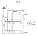
- FIG. 1 is a diagram showing a mobile communication terminal including a DC-DC converter according to an exemplary embodiment of the present invention.
- FIG. 1 shows a display unit 20 related to the subject matter of the present invention and components related to a DC-DC converter 60, but other components included in a mobile communication terminal are known, and therefore they are not shown in FIG. 1 and will be omitted in the following description.
- the mobile communication terminal may be a cellular phone, a smart phone, etc., that uses a mobile communication network.
- FIG. 2 is a diagram showing a pixel of a display unit according to the exemplary embodiment of the present invention.
- FIG. 2 shows pixels connected to an n-th scan line Sn and an m-th data line Dn.
- the mobile communication terminal is configured to include a display unit 20, a scan driver 30, a data driver 40, and a DC-DC converter 60.
- the mobile communication terminal may further include a timing controller for controlling the scan driver 30 and the data driver 40.
- the display unit 20 displays various screens such as a user interface image (UI) on the mobile communication terminal.
- UI user interface image
- the display unit 20 may be an organic light emitting display.
- the display unit 20 is formed of a plurality of pixels 10 connected to scan lines S1 to Sn and data lines D1 to Dm.
- each pixel 10 is connected to a first power supply ELVDD and a second power supply ELVSS, and each of pixel 10 supplied with a first voltage ELVDD' of the first power supply ELVDD and a second voltage ELVSS' of the second power supply ELVSS, generates light corresponding to data signals in accordance with the current flowing to the second power supply ELVSS from the first power supply ELVDD via an organic light emitting diode.
- each pixel 10 includes an organic light emitting diode (OLED) and a pixel circuit 12 connected to the data line Dm and the scan line Sn to control the organic light emitting diode (OLED).
- OLED organic light emitting diode
- An anode electrode of the organic light emitting diode (OLED) is connected to the pixel circuit 12, and a cathode electrode thereof is connected to the second power supply ELVSS.
- OLED organic light emitting diode
- the pixel circuit 12 controls the amount of current supplied to the organic light emitting diode (OLED) in accordance with the data signals supplied to the data line
- the pixel circuit 12 is configured to include a second transistor M2 connected between the first power supply ELVDD and the organic light emitting diode OLED, a first transistor M1 connected between the second transistor M2 and the data line Dm and is controlled by the scan line Sn, and a storage capacitor Cst connected between the gate electrode and the first electrode of the second transistor M2.
- the gate electrode of the first transistor M1 is connected to the scan line Sn, and the first electrode is connected to the data line Dm.
- the second electrode of the first transistor M1 is connected to one terminal of the storage capacitor Cst.
- the first electrode is set as any one of a source electrode and a drain electrode, and the second electrode is set as an electrode different from the first electrode. For example, when the first electrode is set as the source electrode, the second electrode is set as the drain electrode.
- the first transistor M1 connected to the scan line Sn and the data line Sm supplies the data signal supplied from the data line Dm to the storage capacitor Cst when the scan signal is supplied from the scan line Sn.
- the storage capacitor Cst charges the voltage corresponding to the data signal.
- the gate electrode of the second transistor M2 is connected to one terminal of the storage capacitor Cst, and the first electrode of the second transistor M2 is connected to other terminal of the storage capacitor Cst and the first power supply ELVDD.
- the second electrode of the second transistor M2 is connected to the anode electrode of the organic light emitting diode (OLED).
- the second transistor M2 controls the amount of current flowing to the second power supply ELVSS from the first power supply ELVDD via the organic light emitting diode OLED corresponding to the voltage value stored in the storage capacitor Cst.
- the organic light emitting diode (OLED) generates light corresponding to the amount of current supplied from the second transistor M2.
- the scan driver 30 generates the scan signals by the control of the timing controller 50 and supplies the generated scan signals to the scan lines S1 to Sn.
- the data driver 40 generates the data signals by the control of the timing controller 50 and supplies the generated data signals to the data lines D1 to Dm.
- FIG. 3 is a diagram showing the DC-DC converter according to the exemplary embodiment of the present invention.
- the DC-DC converter 60 converts input power Vin and generates the first power ELVDD' of the first power supply ELVDD and the second power ELVSS' of the second power supply ELVSS and supplies them to the display unit 20. In other words, an input voltage Vin is converted to generate a first voltage ELVDD' and a second voltage ELVSS'.
- the DC-DC converter 60 includes a resistor unit 100 electrically connecting a set or predetermined resistor R to a first output terminal OUT1 from which the first voltage ELVDD' is output, when the input voltage Vin is in a specific range.
- the flicker phenomenon occurring in the display unit 20 may be removed by changing the pulse skip mode into either a discontinuous mode (DCM) or a continuous mode by increasing the load of the first output terminal OUT1 which is done by connecting the first output terminal OUT1 to the resistor R.
- DCM discontinuous mode
- a continuous mode by increasing the load of the first output terminal OUT1 which is done by connecting the first output terminal OUT1 to the resistor R.
- the DC-DC converter 60 further includes a boost circuit 80 and a buck circuit 90, together with the resistor unit 100.
- the boost circuit 80 which is a boost converter, generates the first voltage ELVDD' boosting the input Vin applied to the input terminal INPUT and outputs the first voltage ELVDD' to the first output terminal OUT1.
- the buck circuit 90 which is a buck converter, generates the second voltage ELVSS' bucking the input voltage Vin applied to the input terminal INPUT and outputs the second voltage ELVSS' to the second output terminal OUT1.
- the boost circuit 80 and the buck circuit 90 may be formed to have any suitable configuration as long as they are formed for boosting and bucking voltage and also may use any suitable circuit.
- the first power supply ELVDD is a power supply boosting the input voltage Vin and the second power supply ELVSS is a power supply bucking the input voltage Vin, such that the first power supply ELVDD supplies voltage larger (higher in voltage level) than the second power supply ELVSS.
- the input voltage Vin may be transferred from, or provided by, the battery 70 installed in the mobile communication terminal.
- the resistor unit 100 includes a resistor R, a switching element T1, and a comparator 110.
- the resistor R is a device having a set or predetermined resistance value, wherein the resistance value may be variously changed according to experiment or the characteristics of the converter, etc.
- the switching element T1 is disposed between the first output terminal OUT1 outputting the first voltage ELVDD' and the resistor R and is on/off controlled by a comparison signal Vcmp transferred from the comparator 110.
- FIG. 3 shows the case where the switching element T1 is configured as an NMOS type transistor as an exemplary embodiment, but the present invention is not limited thereto.
- the comparator 100 compares the input voltage Vin with reference voltage Vref to perform the on/off control of the switching element T1 through the comparison signal Vcmp.
- the switching element T1 when the input voltage Vin is larger than the reference voltage Vref, the switching element T1 is turned on to connect the resistor R to the first output terminal OUT1, and when the input voltage Vin is lower than the reference voltage Vref, the switching device T1 is turned off to disconnect the resistor R from the first output terminal OUT1.
- the comparator 110 supplies the high-level comparison signal Vcmp to the gate electrode of the transistor when the input voltage Vin is larger than the reference voltage Vref, to turn on the switching element T1, and supplies the low-level comparison signal Vcmp to the gate electrode of the transistor when the input voltage Vin is lower than the reference voltage Vref, to turn off the switching element T1.
- the reference voltage Vref that is a comparison reference may be 4V. That is, when the input voltage Vin is fluctuated above 4V, the resistor R may be connected to the first output terminal OUT1 by determining the fluctuation of the input voltage Vin.
- FIG. 3 shows the case where the resistor unit 100 of the present invention is installed in the DC-DC converter 60 including both the boost circuit 80 and the buck circuit 90, but the resistor unit 100 according to an embodiment of the present invention may be installed in the DC-DC converter including only the boost circuit 80.
Abstract
A DC-DC converter for converting an input voltage to generate a first voltage and for outputting the first voltage to a first output terminal, the DC-DC converter including: a resistor unit for electrically connecting a set resistor to the first output terminal when the input voltage is in a specific range, and a mobile communication terminal using the same. Here, the DC-DC converter is capable of reducing or removing a pulse skip mode by increasing a load of an output end if it is determined that the input voltage is in the specific range, by sensing the input voltage.
Description
- The following description relates to a DC-DC converter and a mobile communication terminal using the same, and more particularly, to a DC-DC converter capable of reducing or removing a pulse skip mode by increasing a load of an output terminal when an input voltage is in a specific range and a mobile communication terminal using the same.
- With the development of mobile communications, a mobile communication terminal (such as a smart phone, etc.) has been prevalently distributed. The mobile communication terminal includes a display unit to display images.
- Power needed to drive the display unit is transferred from a DC-DC converter. The DC-DC converter uses pulse width modulation (PWM) to boost or reduce battery power in order to convert the power into DC power desired at a load side and to supply the DC power.
- Since the length of time the battery is used in an available range is important, the DC-DC converter is operated in a pulse skip mode (PSM) in order to increase efficiency by removing a switching operation performed when a user interface (UI) screen having low driving voltage, or the like is displayed on the display unit.
- However, when a call is made during the pulse skip mode, the battery power is unstably fluctuated and a flicker phenomenon occurs in the display unit. The problem is more of an issue in the case of a terminal using, e.g., a global system for mobile communication (GSM) scheme, that is a digital mobile communication scheme.
- Aspects of embodiments of the present invention are directed toward a DC-DC converter capable of reducing or removing a pulse skip mode by increasing a load of an output terminal if it is determined that an voltage of an input power is in a specific range by sensing the input power and a mobile communication terminal using the same.
- According to an exemplary embodiment of the present invention, a DC-DC converter converting an input power to generate a first power and outputting the first power to a first output terminal includes: a resistor unit electrically connecting a set or predetermined resistor to the first output terminal when a voltage of the input power is in a specific range.
- The DC-DC converter may further include: a boost circuit boosting the input power to generate the first power and outputting the first power to the first output terminal; and a buck circuit bucking the input power to generate a second power and outputting the second power to a second output terminal.
- The resistor unit may include: the set resistor; a switching element disposed between the set resistor and the first output terminal; and a comparator turning-on the switching device when the voltage of the input power is larger than the reference voltage, and turning-off the switching element when the voltage of the input power is lower than the reference voltage.
- The reference voltage may be 4V.
- The input power may be transferred from a battery.
- According to another exemplary embodiment of the present invention, a mobile communication terminal includes: a display unit for displaying images, the display unit including scan lines, data lines crossing the scan lines, and pixels at crossing regions of the scan lines and the data lines, the pixels being connected to both a first power supply and a second power supply; a scan driver supplying scan signals to the pixels through the scan lines; a data driver supplying data signals to the pixels through the data lines; and a DC-DC converter converting an input power to generate a first power of the first power supply and a second power of the second power supply and outputting the first power to a first output terminal and the second power to a second output terminal, wherein the DC-DC converter includes a resistor unit electrically connecting a set or predetermined resistor to the first output terminal when a voltage of the input power is in a specific range.
- As set forth above, in an exemplary embodiment of the present invention, the DC-DC converter is capable of reducing or removing the pulse skip mode by increasing the load of the output terminal if it is determined that the voltage of the input power is in a specific range, by sensing the input voltage.
- The accompanying drawings, together with the specification, illustrate exemplary embodiments of the present invention, and, together with the description, serve to explain the principles of the present invention.
-
FIG. 1 is a diagram showing a mobile communication terminal including a DC-DC converter according to an exemplary embodiment of the present invention; -
FIG. 2 is a diagram showing a pixel of a display unit according to the exemplary embodiment of the present invention; and -
FIG. 3 is a diagram showing the DC-DC converter according to the exemplary embodiment of the present invention. -
FIG. 1 is a diagram showing a mobile communication terminal including a DC-DC converter according to an exemplary embodiment of the present invention. In particular,FIG. 1 shows adisplay unit 20 related to the subject matter of the present invention and components related to a DC-DC converter 60, but other components included in a mobile communication terminal are known, and therefore they are not shown inFIG. 1 and will be omitted in the following description. - In addition, the mobile communication terminal may be a cellular phone, a smart phone, etc., that uses a mobile communication network.
-
FIG. 2 is a diagram showing a pixel of a display unit according to the exemplary embodiment of the present invention. In particular,FIG. 2 shows pixels connected to an n-th scan line Sn and an m-th data line Dn. - The mobile communication terminal according to the exemplary embodiment of the present invention is configured to include a
display unit 20, ascan driver 30, adata driver 40, and a DC-DC converter 60. In addition, the mobile communication terminal may further include a timing controller for controlling thescan driver 30 and thedata driver 40. - The
display unit 20 displays various screens such as a user interface image (UI) on the mobile communication terminal. In the exemplary embodiment of the present invention, thedisplay unit 20 may be an organic light emitting display. - In addition, the
display unit 20 is formed of a plurality ofpixels 10 connected to scan lines S1 to Sn and data lines D1 to Dm. In addition, eachpixel 10 is connected to a first power supply ELVDD and a second power supply ELVSS, and each ofpixel 10 supplied with a first voltage ELVDD' of the first power supply ELVDD and a second voltage ELVSS' of the second power supply ELVSS, generates light corresponding to data signals in accordance with the current flowing to the second power supply ELVSS from the first power supply ELVDD via an organic light emitting diode. - Referring to
FIG. 2 , eachpixel 10 includes an organic light emitting diode (OLED) and apixel circuit 12 connected to the data line Dm and the scan line Sn to control the organic light emitting diode (OLED). - An anode electrode of the organic light emitting diode (OLED) is connected to the
pixel circuit 12, and a cathode electrode thereof is connected to the second power supply ELVSS. - The above-mentioned organic light emitting diode (OLED) generates light having set or predetermined luminance corresponding to current supplied from the
pixel circuit 12. - The
pixel circuit 12 controls the amount of current supplied to the organic light emitting diode (OLED) in accordance with the data signals supplied to the data line - Dm when the scan signals are supplied to the scan line Sn. To this end, the
pixel circuit 12 is configured to include a second transistor M2 connected between the first power supply ELVDD and the organic light emitting diode OLED, a first transistor M1 connected between the second transistor M2 and the data line Dm and is controlled by the scan line Sn, and a storage capacitor Cst connected between the gate electrode and the first electrode of the second transistor M2. - Here, the gate electrode of the first transistor M1 is connected to the scan line Sn, and the first electrode is connected to the data line Dm. The second electrode of the first transistor M1 is connected to one terminal of the storage capacitor Cst. In this configuration, the first electrode is set as any one of a source electrode and a drain electrode, and the second electrode is set as an electrode different from the first electrode. For example, when the first electrode is set as the source electrode, the second electrode is set as the drain electrode.
- The first transistor M1 connected to the scan line Sn and the data line Sm supplies the data signal supplied from the data line Dm to the storage capacitor Cst when the scan signal is supplied from the scan line Sn. In this case, the storage capacitor Cst charges the voltage corresponding to the data signal.
- The gate electrode of the second transistor M2 is connected to one terminal of the storage capacitor Cst, and the first electrode of the second transistor M2 is connected to other terminal of the storage capacitor Cst and the first power supply ELVDD. The second electrode of the second transistor M2 is connected to the anode electrode of the organic light emitting diode (OLED).
- The second transistor M2 controls the amount of current flowing to the second power supply ELVSS from the first power supply ELVDD via the organic light emitting diode OLED corresponding to the voltage value stored in the storage capacitor Cst. In this case, the organic light emitting diode (OLED) generates light corresponding to the amount of current supplied from the second transistor M2. The above-mentioned pixel structure of
FIG. 2 is only the exemplary embodiment of the present invention, and thepixel 10 of the present invention is not limited to the pixel structure ofFIG. 2 . - The
scan driver 30 generates the scan signals by the control of thetiming controller 50 and supplies the generated scan signals to the scan lines S1 to Sn. - The
data driver 40 generates the data signals by the control of thetiming controller 50 and supplies the generated data signals to the data lines D1 to Dm. -
FIG. 3 is a diagram showing the DC-DC converter according to the exemplary embodiment of the present invention. - The DC-
DC converter 60 converts input power Vin and generates the first power ELVDD' of the first power supply ELVDD and the second power ELVSS' of the second power supply ELVSS and supplies them to thedisplay unit 20. In other words, an input voltage Vin is converted to generate a first voltage ELVDD' and a second voltage ELVSS'. - In particular, the DC-
DC converter 60 includes aresistor unit 100 electrically connecting a set or predetermined resistor R to a first output terminal OUT1 from which the first voltage ELVDD' is output, when the input voltage Vin is in a specific range. - Therefore, when the input voltage Vin is in the specific range and when a call is placed during the pulse skip mode, the flicker phenomenon occurring in the
display unit 20 may be removed by changing the pulse skip mode into either a discontinuous mode (DCM) or a continuous mode by increasing the load of the first output terminal OUT1 which is done by connecting the first output terminal OUT1 to the resistor R. - Referring to
FIG. 3 , the DC-DC converter 60 further includes aboost circuit 80 and abuck circuit 90, together with theresistor unit 100. - The
boost circuit 80, which is a boost converter, generates the first voltage ELVDD' boosting the input Vin applied to the input terminal INPUT and outputs the first voltage ELVDD' to the first output terminal OUT1. - The
buck circuit 90, which is a buck converter, generates the second voltage ELVSS' bucking the input voltage Vin applied to the input terminal INPUT and outputs the second voltage ELVSS' to the second output terminal OUT1. - The
boost circuit 80 and thebuck circuit 90 may be formed to have any suitable configuration as long as they are formed for boosting and bucking voltage and also may use any suitable circuit. - The first power supply ELVDD is a power supply boosting the input voltage Vin and the second power supply ELVSS is a power supply bucking the input voltage Vin, such that the first power supply ELVDD supplies voltage larger (higher in voltage level) than the second power supply ELVSS.
- The input voltage Vin may be transferred from, or provided by, the
battery 70 installed in the mobile communication terminal. - In the exemplary embodiment of the present invention, the
resistor unit 100 includes a resistor R, a switching element T1, and acomparator 110. - The resistor R is a device having a set or predetermined resistance value, wherein the resistance value may be variously changed according to experiment or the characteristics of the converter, etc.
- The switching element T1 is disposed between the first output terminal OUT1 outputting the first voltage ELVDD' and the resistor R and is on/off controlled by a comparison signal Vcmp transferred from the
comparator 110.FIG. 3 shows the case where the switching element T1 is configured as an NMOS type transistor as an exemplary embodiment, but the present invention is not limited thereto. - The
comparator 100 compares the input voltage Vin with reference voltage Vref to perform the on/off control of the switching element T1 through the comparison signal Vcmp. - In more detail, when the input voltage Vin is larger than the reference voltage Vref, the switching element T1 is turned on to connect the resistor R to the first output terminal OUT1, and when the input voltage Vin is lower than the reference voltage Vref, the switching device T1 is turned off to disconnect the resistor R from the first output terminal OUT1.
- Describing the case where the switching device T1 is the NMOS type transistor as an example, the
comparator 110 supplies the high-level comparison signal Vcmp to the gate electrode of the transistor when the input voltage Vin is larger than the reference voltage Vref, to turn on the switching element T1, and supplies the low-level comparison signal Vcmp to the gate electrode of the transistor when the input voltage Vin is lower than the reference voltage Vref, to turn off the switching element T1. - In this case, the reference voltage Vref that is a comparison reference may be 4V. That is, when the input voltage Vin is fluctuated above 4V, the resistor R may be connected to the first output terminal OUT1 by determining the fluctuation of the input voltage Vin.
-
FIG. 3 shows the case where theresistor unit 100 of the present invention is installed in the DC-DC converter 60 including both theboost circuit 80 and thebuck circuit 90, but theresistor unit 100 according to an embodiment of the present invention may be installed in the DC-DC converter including only theboost circuit 80. - While the present invention has been described in connection with certain exemplary embodiments, it is to be understood that the invention is not limited to the disclosed embodiments, but, on the contrary, is intended to cover various modifications and equivalent arrangements included within the scope of the appended claims.
Claims (6)
- A DC-DC converter for converting an input voltage to generate a first voltage and for outputting the first voltage to a first output terminal, the DC-DC converter comprising:a resistor unit for electrically connecting a set resistor to the first output terminal when the input voltage is in a specific range.
- The DC-DC converter according to claim 1, further comprising:a boost circuit for boosting the input voltage to generate the first voltage and for outputting the first voltage to the first output terminal; anda buck circuit for bucking the input voltage to generate a second voltage and for outputting the second voltage to a second output terminal.
- The DC-DC converter according to claim 1 or 2, wherein the resistor unit comprises:the set resistor;a switching element between the set resistor and the first output terminal; anda comparator for turning on the switching element when the input voltage is larger than a reference voltage, and for turning off the switching element when the input voltage is lower than the reference voltage.
- The DC-DC converter according to claim 3, wherein the reference voltage is 4V.
- The DC-DC converter according to any one of the preceding claims, wherein the input voltage is provided by a battery.
- A mobile communication terminal, comprising:a display unit for displaying images, the display unit comprising scan lines, data lines crossing the scan lines, and pixels at crossing regions of the scan lines and the data lines, the pixels being connected to both a first power supply and a second power supply;a scan driver for supplying scan signals to the pixels through the scan lines;a data driver for supplying data signals to the pixels through the data lines; anda DC-DC converter according to any one of the preceding claims.
Applications Claiming Priority (1)
| Application Number | Priority Date | Filing Date | Title |
|---|---|---|---|
| KR1020110001418A KR101788218B1 (en) | 2011-01-06 | 2011-01-06 | DC-DC Converter and Mobile Communication Terminal using The Same |
Publications (1)
| Publication Number | Publication Date |
|---|---|
| EP2475083A2 true EP2475083A2 (en) | 2012-07-11 |
Family
ID=44992793
Family Applications (1)
| Application Number | Title | Priority Date | Filing Date |
|---|---|---|---|
| EP11190064A Withdrawn EP2475083A2 (en) | 2011-01-06 | 2011-11-22 | DC-DC converter and mobile communication terminal using the same |
Country Status (3)
| Country | Link |
|---|---|
| US (1) | US8643637B2 (en) |
| EP (1) | EP2475083A2 (en) |
| KR (1) | KR101788218B1 (en) |
Families Citing this family (6)
| Publication number | Priority date | Publication date | Assignee | Title |
|---|---|---|---|---|
| US20130271102A1 (en) * | 2012-04-12 | 2013-10-17 | Roger Lin | Power supply control structure |
| KR102592901B1 (en) * | 2016-02-26 | 2023-10-24 | 삼성디스플레이 주식회사 | Dc-dc converter, method of dc-dc converting using the same and display apparatus having the same |
| US10461555B2 (en) | 2017-05-18 | 2019-10-29 | Dialog Semiconductor (Uk) Limited | Battery charging for mobile devices |
| KR20210122932A (en) | 2020-04-01 | 2021-10-13 | 삼성디스플레이 주식회사 | Power management circuit, method of generating a pixel power supplly voltage, and display device |
| US20230105095A1 (en) * | 2021-10-01 | 2023-04-06 | Samsung Electronics Co., Ltd. | Electronic device and method of operating the same |
| CN115472125B (en) * | 2022-08-26 | 2024-02-27 | 惠科股份有限公司 | Driving circuit of display panel and display device |
Family Cites Families (34)
| Publication number | Priority date | Publication date | Assignee | Title |
|---|---|---|---|---|
| US3590361A (en) * | 1969-12-31 | 1971-06-29 | Bell Telephone Labor Inc | Dc to dc converter including switching device having its on and off times independently controlled by the line and load voltages, respectively |
| US4124884A (en) * | 1977-03-07 | 1978-11-07 | Bell Telephone Laboratories, Incorporated | DC to DC converter with regulated input impedance |
| US4210958A (en) * | 1978-10-25 | 1980-07-01 | Tsuneo Ikenoue | DC-DC Converter output stabilizing device |
| US6424130B1 (en) * | 1999-04-27 | 2002-07-23 | Seiko Instruments Inc. | Output voltage detecting circuit |
| US6466188B1 (en) * | 2000-01-20 | 2002-10-15 | International Business Machines Corporation | DC-DC converter with current sensing for use with non-linear devices |
| KR100348275B1 (en) * | 2000-07-28 | 2002-08-09 | 엘지전자 주식회사 | driving control circuit in organic electroluminescence |
| JP4873677B2 (en) * | 2001-09-06 | 2012-02-08 | 東北パイオニア株式会社 | Driving device for light emitting display panel |
| TWI269513B (en) * | 2004-05-21 | 2006-12-21 | Delta Electronics Inc | Power converter that supplies multiple output voltages via adaptor |
| US8013583B2 (en) * | 2004-07-01 | 2011-09-06 | Xslent Energy Technologies, Llc | Dynamic switch power converter |
| US7161333B2 (en) | 2004-12-08 | 2007-01-09 | Linear Technology Corporation | System and method for determining load current in switching regulators operable in pulse skipping mode |
| EP1693948B1 (en) * | 2005-02-22 | 2008-04-09 | STMicroelectronics S.r.l. | Secondary side post regulator with PWM |
| US8134548B2 (en) * | 2005-06-30 | 2012-03-13 | Micron Technology, Inc. | DC-DC converter switching transistor current measurement technique |
| US7948455B2 (en) * | 2005-10-20 | 2011-05-24 | 02Micro Inc. | Apparatus and method for regulating white LEDs |
| JP4851203B2 (en) * | 2006-02-24 | 2012-01-11 | ルネサスエレクトロニクス株式会社 | Power supply selection detection circuit and power supply control method |
| KR100732851B1 (en) | 2006-06-05 | 2007-06-27 | 삼성에스디아이 주식회사 | Dc/dc converter and organic light emitting display using the same |
| KR20080064564A (en) * | 2007-01-05 | 2008-07-09 | 삼성전자주식회사 | Printed circuit board and liquid crystal display device having the same |
| KR100833764B1 (en) | 2007-01-22 | 2008-05-29 | 삼성에스디아이 주식회사 | Organic light emitting display having dc-dc converter |
| JP4363457B2 (en) * | 2007-05-01 | 2009-11-11 | ヤマハ株式会社 | Power control device, speaker device, and power control method |
| US7944420B2 (en) * | 2007-09-28 | 2011-05-17 | Osram Sylvania Inc. | Light emitting diode driver providing current and power control |
| KR101624501B1 (en) * | 2007-10-17 | 2016-06-08 | 삼성디스플레이 주식회사 | Gate off voltage generating circuit, Driving device and Liquid crystal display comprising the same |
| KR20090050318A (en) | 2007-11-15 | 2009-05-20 | 삼성전자주식회사 | Power converter having auto conversion function for pulse skip mode and control method of thereof |
| US7924019B2 (en) * | 2008-01-16 | 2011-04-12 | Lear Corporation | System and method for fault isolation and leakage current detection |
| JP5205083B2 (en) * | 2008-03-07 | 2013-06-05 | ルネサスエレクトロニクス株式会社 | Power supply |
| KR100952834B1 (en) * | 2008-08-06 | 2010-04-15 | 삼성모바일디스플레이주식회사 | Dc-dc converter and organic light emitting display using the same |
| JP4666096B2 (en) * | 2008-09-04 | 2011-04-06 | 株式会社デンソー | DC-DC converter |
| JP2010118999A (en) * | 2008-11-14 | 2010-05-27 | Toshiba Corp | Semiconductor integrated circuit |
| KR101064462B1 (en) * | 2009-11-17 | 2011-09-15 | 삼성모바일디스플레이주식회사 | Dc-dc converter and organic light emitting display device for the same |
| KR101101094B1 (en) * | 2010-02-03 | 2012-01-03 | 삼성모바일디스플레이주식회사 | Dc-dc converter and organic light emitting display device for the same |
| KR101146989B1 (en) * | 2010-05-06 | 2012-05-22 | 삼성모바일디스플레이주식회사 | DC-DC converter, Organic electro luminescence Display having the same and driving method thereof |
| KR101097352B1 (en) * | 2010-05-06 | 2011-12-23 | 삼성모바일디스플레이주식회사 | DC-DC converter, driving method thereof, organic electro luminescence Display having the same and driving method thereof |
| US8487924B2 (en) * | 2010-08-25 | 2013-07-16 | Dongwoon Anatech Co., Ltd. | Apparatus for driving of display panel |
| US8427130B2 (en) * | 2010-12-16 | 2013-04-23 | Integrated Device Technology, Inc. | Methods and apparatuses for combined frequency compensation and soft start processes |
| KR101829398B1 (en) * | 2011-06-30 | 2018-02-20 | 삼성디스플레이 주식회사 | Organic Light Emitting Display and Driving Method Thereof |
| KR101871906B1 (en) * | 2011-06-30 | 2018-06-28 | 삼성디스플레이 주식회사 | DC-DC Converter and Organic Light Emitting Display including The Same |
-
2011
- 2011-01-06 KR KR1020110001418A patent/KR101788218B1/en active IP Right Grant
- 2011-09-28 US US13/247,897 patent/US8643637B2/en active Active
- 2011-11-22 EP EP11190064A patent/EP2475083A2/en not_active Withdrawn
Non-Patent Citations (1)
| Title |
|---|
| None |
Also Published As
| Publication number | Publication date |
|---|---|
| KR20120080007A (en) | 2012-07-16 |
| US8643637B2 (en) | 2014-02-04 |
| US20120176361A1 (en) | 2012-07-12 |
| KR101788218B1 (en) | 2017-10-20 |
Similar Documents
| Publication | Publication Date | Title |
|---|---|---|
| US9123286B2 (en) | Power generator having a power selector and organic light emitting display device using the same | |
| JP7083929B2 (en) | DC-DC converter | |
| US9875692B2 (en) | DC-DC converter and organic light emitting display including the same | |
| US9535440B2 (en) | DC-DC converter and organic light emitting display device using the same | |
| EP1978504B1 (en) | Organic light emitting diode (OLED) display and a method of driving the same | |
| KR101064462B1 (en) | Dc-dc converter and organic light emitting display device for the same | |
| US10325548B2 (en) | Power converter, display device including power converter, and method of operating power converter | |
| US8643637B2 (en) | DC-DC converter and mobile communication terminal using the same | |
| CN106160469B (en) | DC-DC converter and organic light emitting display device having the same | |
| US10170047B2 (en) | Organic light emitting display and driving method thereof | |
| US20100033467A1 (en) | Dc-dc converter and organic light emitting display device using the same | |
| US9548649B2 (en) | DC-DC converter and display device including the same | |
| US9414461B2 (en) | DC-DC converter and organic light emitting display device including the same | |
| US20150236594A1 (en) | Independent Output Control for Single-Inductor, Bipolar Outputs, Buck-Boost Converters | |
| KR101554583B1 (en) | Organic electroluminescent display and method of driving the same | |
| CN113422510A (en) | DC-DC converter | |
| KR102116565B1 (en) | Dc-dc converter and organic light emitting display including the same | |
| KR20130095401A (en) | Backlight driver and liquid crystal display device including the same |
Legal Events
| Date | Code | Title | Description |
|---|---|---|---|
| PUAI | Public reference made under article 153(3) epc to a published international application that has entered the european phase |
Free format text: ORIGINAL CODE: 0009012 |
|
| AK | Designated contracting states |
Kind code of ref document: A2 Designated state(s): AL AT BE BG CH CY CZ DE DK EE ES FI FR GB GR HR HU IE IS IT LI LT LU LV MC MK MT NL NO PL PT RO RS SE SI SK SM TR |
|
| AX | Request for extension of the european patent |
Extension state: BA ME |
|
| RAP1 | Party data changed (applicant data changed or rights of an application transferred) |
Owner name: SAMSUNG DISPLAY CO., LTD. |
|
| RAP1 | Party data changed (applicant data changed or rights of an application transferred) |
Owner name: SAMSUNG DISPLAY CO., LTD. |
|
| STAA | Information on the status of an ep patent application or granted ep patent |
Free format text: STATUS: THE APPLICATION HAS BEEN WITHDRAWN |
|
| 18W | Application withdrawn |
Effective date: 20170726 |