EP1852756A1 - Clock signal outputting device and its control method, and electronic device and its control method - Google Patents
Clock signal outputting device and its control method, and electronic device and its control method Download PDFInfo
- Publication number
- EP1852756A1 EP1852756A1 EP06714542A EP06714542A EP1852756A1 EP 1852756 A1 EP1852756 A1 EP 1852756A1 EP 06714542 A EP06714542 A EP 06714542A EP 06714542 A EP06714542 A EP 06714542A EP 1852756 A1 EP1852756 A1 EP 1852756A1
- Authority
- EP
- European Patent Office
- Prior art keywords
- clock signal
- oscillator
- accuracy
- section
- correction data
- Prior art date
- Legal status (The legal status is an assumption and is not a legal conclusion. Google has not performed a legal analysis and makes no representation as to the accuracy of the status listed.)
- Granted
Links
- 238000000034 method Methods 0.000 title claims abstract description 46
- 238000012937 correction Methods 0.000 claims abstract description 151
- 239000010453 quartz Substances 0.000 claims abstract description 72
- VYPSYNLAJGMNEJ-UHFFFAOYSA-N silicon dioxide Inorganic materials O=[Si]=O VYPSYNLAJGMNEJ-UHFFFAOYSA-N 0.000 claims abstract description 72
- 238000006073 displacement reaction Methods 0.000 claims abstract description 16
- 238000001514 detection method Methods 0.000 claims description 47
- 230000008859 change Effects 0.000 claims description 39
- 239000013078 crystal Substances 0.000 claims description 21
- 230000003679 aging effect Effects 0.000 claims description 12
- 230000005484 gravity Effects 0.000 claims description 3
- 230000010355 oscillation Effects 0.000 description 42
- 230000008569 process Effects 0.000 description 25
- 238000010586 diagram Methods 0.000 description 17
- 230000010363 phase shift Effects 0.000 description 8
- 230000032683 aging Effects 0.000 description 7
- 230000007246 mechanism Effects 0.000 description 7
- 239000003990 capacitor Substances 0.000 description 6
- 230000007774 longterm Effects 0.000 description 6
- 239000004973 liquid crystal related substance Substances 0.000 description 4
- 230000001419 dependent effect Effects 0.000 description 3
- 229910052792 caesium Inorganic materials 0.000 description 2
- TVFDJXOCXUVLDH-UHFFFAOYSA-N caesium atom Chemical compound [Cs] TVFDJXOCXUVLDH-UHFFFAOYSA-N 0.000 description 2
- 101150110971 CIN7 gene Proteins 0.000 description 1
- 101150110298 INV1 gene Proteins 0.000 description 1
- WHXSMMKQMYFTQS-UHFFFAOYSA-N Lithium Chemical compound [Li] WHXSMMKQMYFTQS-UHFFFAOYSA-N 0.000 description 1
- XUIMIQQOPSSXEZ-UHFFFAOYSA-N Silicon Chemical compound [Si] XUIMIQQOPSSXEZ-UHFFFAOYSA-N 0.000 description 1
- BQCADISMDOOEFD-UHFFFAOYSA-N Silver Chemical compound [Ag] BQCADISMDOOEFD-UHFFFAOYSA-N 0.000 description 1
- 101100397044 Xenopus laevis invs-a gene Proteins 0.000 description 1
- 230000003213 activating effect Effects 0.000 description 1
- 230000004913 activation Effects 0.000 description 1
- 230000008901 benefit Effects 0.000 description 1
- 239000000919 ceramic Substances 0.000 description 1
- 230000000295 complement effect Effects 0.000 description 1
- 238000013461 design Methods 0.000 description 1
- 230000000694 effects Effects 0.000 description 1
- 230000005684 electric field Effects 0.000 description 1
- 230000004907 flux Effects 0.000 description 1
- 230000010354 integration Effects 0.000 description 1
- 229910052744 lithium Inorganic materials 0.000 description 1
- 238000005259 measurement Methods 0.000 description 1
- 230000010358 mechanical oscillation Effects 0.000 description 1
- 238000004377 microelectronic Methods 0.000 description 1
- 238000012986 modification Methods 0.000 description 1
- 230000004048 modification Effects 0.000 description 1
- 238000010248 power generation Methods 0.000 description 1
- 230000009467 reduction Effects 0.000 description 1
- 230000004044 response Effects 0.000 description 1
- 230000000717 retained effect Effects 0.000 description 1
- 229910052701 rubidium Inorganic materials 0.000 description 1
- IGLNJRXAVVLDKE-UHFFFAOYSA-N rubidium atom Chemical compound [Rb] IGLNJRXAVVLDKE-UHFFFAOYSA-N 0.000 description 1
- 229910052710 silicon Inorganic materials 0.000 description 1
- 239000010703 silicon Substances 0.000 description 1
- 229910052709 silver Inorganic materials 0.000 description 1
- 239000004332 silver Substances 0.000 description 1
- 239000000758 substrate Substances 0.000 description 1
- XLYOFNOQVPJJNP-UHFFFAOYSA-N water Substances O XLYOFNOQVPJJNP-UHFFFAOYSA-N 0.000 description 1
Images






Classifications
-
- G—PHYSICS
- G04—HOROLOGY
- G04G—ELECTRONIC TIME-PIECES
- G04G3/00—Producing timing pulses
-
- G—PHYSICS
- G04—HOROLOGY
- G04C—ELECTROMECHANICAL CLOCKS OR WATCHES
- G04C13/00—Driving mechanisms for clocks by primary clocks
-
- G—PHYSICS
- G04—HOROLOGY
- G04F—TIME-INTERVAL MEASURING
- G04F5/00—Apparatus for producing preselected time intervals for use as timing standards
- G04F5/14—Apparatus for producing preselected time intervals for use as timing standards using atomic clocks
Definitions
- the present invention relates to a clock signal output unit being equipped with a reference oscillator that generates a reference clock signal, and generating an output clock signal of a predetermined frequency from the reference clock signal for output, and a control method thereof, and an electronic device and a control method thereof.
- an electronic clock generates a signal of 1Hz, for example, by frequency-dividing a reference clock signal coming from a reference oscillator, and counts the time based on this 1Hz signal.
- the electronic clock of such a type is well known by a annual rate timepiece, which implements an error of ⁇ a few tens of seconds per year using a temperature compensated crystal oscillator for a reference oscillator (as an example, Patent Document 1).
- Patent Documents 2 and 3 a standard oscillator using an atomic oscillator is proposed (as examples, Patent Documents 2 and 3) .
- the issue here is that, in the conventional temperature compensated crystal oscillator, the temperature properties of a quartz crystal having the third-order properties are temperature-compensated by the temperature properties of a capacity having the second-order properties, thereby causing some temperature change to an oscillation frequency. Moreover, with the crystal oscillator of such a type, the aging properties of the quartz crystal causes some change to the oscillation frequency over the long terms, thereby resulting in poorer frequency accuracy compared with an atomic oscillator.
- the present invention is proposed in consideration of the above-described circumstances, and an object thereof is to provide a clock signal output unit that can increase the accuracy of a clock signal while avoiding the increase of the entire power consumption even with a high-accuracy oscillator relatively high in power consumption, and a control method thereof, and an electronic device and a control method thereof.
- the present invention is directed to a clock signal output unit being equipped with a reference oscillator that generates a reference clock signal, and generating, from the reference clock signal, an output clock signal of a predetermined frequency for output.
- the unit is characterized by including: a high-accuracy oscillator that generates a high-accuracy clock signal whose accuracy is higher than that of the reference oscillator; an intermittent driving section that drives the high-accuracy oscillator in an intermittent manner; and a correction section that acquires correction data for correcting an amount of displacement observed in the output clock signal with reference to the high-accuracy clock signal every time the high-accuracy oscillator is driven, and corrects the output clock signal based on the correction data.
- This configuration includes the high-accuracy oscillator that generates a high-accuracy clock signal whose accuracy is higher than that of the reference oscillator; the intermittent driving section that drives the high-accuracy oscillator in an intermittent manner; and the correction section that acquires correction data for correcting an amount of displacement observed in the output clock signal with reference to the high-accuracy clock signal every time the high-accuracy oscillator is driven, and corrects the output clock signal based on the correction data. Therefore, even if a high-accuracy oscillator with high power consumption is used, the output clock signal can be increased in accuracy with reference to the high-accuracy oscillator while avoiding the increase of the entire power consumption by stopping the high-accuracy oscillator in an intermittent manner.
- a reference oscillator influence information detection section is provided for detecting reference oscillator influence information affecting the operation of the reference oscillator.
- the intermittent driving section drives the high-accuracy oscillator, and the correction section acquires the correction data.
- the high-accuracy oscillator is driven to acquire the correction data. This enables to quickly correct any frequency change caused by the reference oscillator influence information so that the accuracy of the output clock signal can be increased to a further extent.
- the above configuration includes a reference oscillator influence information detection section that detects reference oscillator influence information affecting the operation of the reference oscillator; and a storage section that stores therein the correction data corresponding to the reference oscillator influence information on a value basis.
- the intermittent driving section drives the high-accuracy oscillator
- the correction section acquires the correction data
- the correction data is stored in the storage section
- the output clock signal is corrected based on this correction data
- the detected reference oscillator influence information is not the first-time-detected value
- the intermittent driving section drives the high-accuracy oscillator, and when the detected reference oscillator influence information is not the value detected for the first time in the correction data update period, the high-accuracy oscillator is kept in a no-drive state.
- the high-accuracy oscillator when the detected reference oscillator influence information is not a value detected for the first time in the correction data update period, the high-accuracy oscillator is kept in a no-drive state so that the power consumption can be favorably reduced.
- the detected reference oscillator influence information is a value detected for the first time in the correction data update period
- the high-accuracy oscillator is driven so that correction data in storage can be updated with any new correction data every time the correction data update period passes. This enables to update the correction data in accordance with any frequency change caused due to the aging properties or others of the reference oscillator so that the accuracy of the output clock signal can be increased to a further extent.
- the reference oscillator influence information includes at least any one of an amount of temperature change, an amount of humidity change, an electric power supply, a posture or a gravity direction of the clock signal output unit.
- the above configuration includes a high-accuracy oscillator influence information detection section that detects high-accuracy oscillator influence information affecting the operation of the high-accuracy oscillator.
- the high-accuracy oscillator is kept in the no-drive state.
- the high-accuracy oscillator is kept in the no-drive state so that a possible case of driving the high-accuracy oscillator in the operation-unstable state can be avoided.
- the high-accuracy oscillator influence information includes at least either a magnetic field or an electric power supply.
- the reference oscillator is small in power consumption compared with the high-accuracy oscillator, and the reference oscillator may be a quartz oscillator, a CR oscillator, or a MEMS oscillator.
- the high-accuracy clock signal may be a signal whose frequency is higher than that of the reference clock signal, and the high-accuracy oscillator may be any one of an atomic oscillator, a temperature compensated oscillator, an oven controlled crystal oscillator, and an oscillator using an AT cut resonator.
- the above configuration may include, alternatively, a comparison section that makes a phase comparison or a frequency comparison between the reference clock signal and the high-accuracy clock signal, and the intermittent driving section may drive the comparison section only during driving the high-accuracy oscillator so as to reduce the power consumption to a further extent.
- the intermittent driving section may gradually lengthen an intermittent driving interval in accordance with the aging properties of the reference oscillator. This configuration enables to reduce the frequency of driving the high-accuracy oscillator while suppressing a frequency change possibly caused by aging so that the power consumption can be reduced.
- the present invention is directed also to a control method of a clock signal output unit being equipped with a reference oscillator that generates a reference clock signal, and generating, from the reference clock signal, an output clock signal of a predetermined frequency for output.
- the method is characterized in that a high-accuracy oscillator that generates a high-accuracy clock signal whose accuracy is higher than that of the reference oscillator is driven in an intermittent manner, and every time the high-accuracy oscillator is driven, correction data is acquired for use for correcting an amount of displacement observed in the output clock signal with reference to the high-accuracy clock signal, and based on the correction data, the output clock signal is corrected.
- the high-accuracy oscillator that generates a high-accuracy clock signal whose accuracy is higher than that of the reference oscillator is driven in an intermittent manner, and every time the high-accuracy oscillator is driven, correction data is acquired for use for correcting an amount of displacement observed in the output clock signal with reference to the high-accuracy clock signal, and based on the correction data, the output clock signal is corrected. Therefore, even if a high-accuracy oscillator with high power consumption is used, the output clock signal can be increased in accuracy while avoiding the increase of the entire power consumption.
- the present invention is directed also to an electronic device equipped with a clock signal output section that generates, from a reference clock signal coming from a reference oscillator, an output clock signal of a predetermined frequency for output.
- the device is characterized by including: a high-accuracy oscillator that generates a high-accuracy clock signal whose accuracy is higher than that of the reference oscillator; an intermittent driving section that drives the high-accuracy oscillator in an intermittent manner; and a correction section that acquires correction data for correcting an amount of displacement observed in the output clock signal with reference to the high-accuracy clock signal every time the high-accuracy oscillator is driven, and corrects the output clock signal based on the correction data.
- This configuration includes the high-accuracy oscillator that generates a high-accuracy clock signal whose accuracy is higher than that of the reference oscillator, the intermittent driving section that drives the high-accuracy oscillator in an intermittent manner, and the correction section that acquires correction data for correcting an amount of displacement observed in the output clock signal with reference to the high-accuracy clock signal every time the high-accuracy oscillator is driven, and corrects the output clock signal based on the correction data. Therefore, even if a high-accuracy oscillator with high power consumption is used, the output clock signal can be increased in accuracy while avoiding the increase of the entire power consumption.
- the electronic device may be configured as a timepiece including a time display section that displays thereon a time based on the output clock signal.
- the electronic device preferably includes therein a power supply section that supplies an operating power to the electronic device. This configuration enables the long-term operation even with an electronic device equipped therein with a power supply section.
- the present invention is directed also to a control method of an electronic device equipped with a clock signal output section that generates, for output, an output clock signal of a predetermined frequency from a reference clock signal coming from a reference oscillator.
- the method is characterized in that a high-accuracy oscillator generating a high-accuracy clock signal whose accuracy is higher than that of the reference oscillator is driven in an intermittent manner, and every time the high-accuracy oscillator is driven, correction data for correcting an amount of displacement observed in the output clock signal is acquired with reference to the high-accuracy clock signal, and the output clock signal is corrected based on the correction data.
- the high-accuracy oscillator generating a high-accuracy clock signal whose accuracy is higher than that of the reference oscillator is driven in an intermittent manner, and every time the high-accuracy oscillator is driven, correction data for correcting an amount of displacement observed in the output clock signal is acquired with reference to the high-accuracy clock signal, and the output clock signal is corrected based on the correction data. Therefore, even if a high-accuracy oscillator with high power consumption is used, the output clock signal can be increased in accuracy while avoiding the increase of the entire power consumption.
- the present invention includes a high-accuracy oscillator that generates a high-accuracy clock signal whose accuracy is higher than that of the reference oscillator; an intermittent driving section that drives the high-accuracy oscillator in an intermittent manner; and a correction section that acquires correction data for correcting an amount of displacement observed in the output clock signal with reference to the high-accuracy clock signal every time the high-accuracy oscillator is driven, and corrects the output clock signal based on the correction data. Therefore, even if a high-accuracy oscillator with high power consumption is used, the output clock signal can be increased in accuracy with reference to the high-accuracy oscillator while avoiding the increase of the entire power consumption by stopping this high-accuracy oscillator in an intermittent manner.
- the high-accuracy oscillator is driven to acquire the correction data. This enables to quickly correct any frequency change caused by the reference oscillator influence information so that the accuracy of the output clock signal can be increased to a further extent.
- the high-accuracy oscillator when the detected reference oscillator influence information is a value detected for the first time in a predetermined correction data update period, the high-accuracy oscillator is driven, and when the detected reference oscillator influence information is not the value detected for the first time in the correction data update period, the high-accuracy oscillator is kept in a no-drive state. Therefore, the frequency of driving the high-accuracy oscillator is reduced, and the power consumption can be thus reduced.
- every time the correction data update period is passed the high-accuracy oscillator is driven so that any new correction data is acquired, and the correction data can be updated in accordance with a frequency change caused due to the aging properties or others of the reference oscillator.
- the output clock signal can be thus increased in accuracy to a further extent.
- the high-accuracy oscillator while the high-accuracy oscillator influence information affecting the operation of the high-accuracy oscillator is detected, the high-accuracy oscillator is kept in the no-drive state. This thus avoids the case of driving the high-accuracy oscillator in the operation-unstable state.
- FIG. 1 is a block diagram showing the configuration of a wristwatch of an embodiment of the present invention.
- This wristwatch (electronic timepiece) 10 is configured to include a hand movement mechanism 11 and a drive section 12 both configuring a timepiece module, and a power supply section 13 that supplies an operating power to this timepiece module.
- the hand movement mechanism 11 configures a time display section that displays thereon the time by driving a second hand 21, a minute hand 22, and an hour hand 23, and as shown in the drawing, includes a gear train 29 in which a second wheel 24, a second wheel 25, and a tube wheel 26 are coupled together via intermediate wheels 27 and 28 to move together.
- the rotation axis of the second wheel 24 is attached with one end of the second hand 21, the rotation axis of the second wheel 25 is attached with one end of the minute hand 22, and the rotation axis of the tube wheel 26 is attached with one end of the hour hand 23.
- the second wheel 24 is meshed with a drive gear 31 of a drive motor 30, and the second wheel 24 is rotate-driven in response to the rotation of the drive motor 30. This rotation is transferred to the second wheel 25 and the tube wheel 26 so that the second hand 21, the minute hand 22, and the hour hand 23 are each rotate-driven. By these hands 21 to 23, the time is displayed.
- the drive section 12 is provided with an oscillation section (clock signal output section) 40 and a motor drive section 50.
- the oscillation section 40 outputs a 1Hz clock signal (output clock signal) CL0, and based on this 1Hz clock signal CL0, the motor drive section 50 supplies a drive pulse to the drive motor 30, thereby driving the drive motor 30.
- this wristwatch 1 may be provided with a liquid crystal display device as an alternative to the hand movement mechanism 11 or in addition to the hand movement mechanism 11, and the liquid crystal display device may be so configured as to display thereon the time.
- the drive section 12 may be provided with a counter for use with a timepiece, counting the 1Hz clock signal CL0, and a liquid crystal drive section that drives the liquid crystal display device based on the count value of the counter for use with a timepiece.
- the power supply section 13 is configured to include a battery 60 disposed inside of this wristwatch 10, and a constant voltage circuit (not shown) that converts the power stored in the battery 60 into a constant voltage for supply to the components of the drive section 12.
- a coin-shaped primary battery such as lithium battery or silver battery.
- this wristwatch 10 may be provided therein with a power generation section such as solar panel, and with this being the case, a secondary battery is applied to the battery 60.
- the oscillation section 40 is provided with a quartz oscillator (reference oscillation section) 41, and an atomic oscillator (high-accuracy oscillator) 42.
- the quartz oscillator 41 is an oscillator that oscillates a fork-type crystal resonator, and outputs a reference clock signal CL1 of 32.768 kHz, for example.
- a cesium atomic oscillator whose frequency accuracy and the frequency stability are higher than those of the quartz oscillator 41, e.g., an oscillator that outputs a clock signal CL2 of 9.2 GHz.
- the cesium atomic oscillator is not restrictive, and any other atomic oscillator (e.g., rubidium atomic oscillator) may be used.
- the quartz oscillator 41 may be any arbitrary quartz oscillator such as oscillator to be used in a annual rate timepiece or in a daily rate timepiece.
- the oscillation section 40 is provided with a frequency division circuit 43 that frequency-divides the reference clock signal CL1 of the quartz oscillator 41.
- This frequency division circuit 43 is configured to include a plurality of frequency dividers that are connected in multistage, including a data-set-function-provided 1/2 frequency division circuit 43a serving as an adjustment amount provision section.
- the frequency division circuit frequency-divides the reference clock signal CL1 to derive 1Hz, and outputs the 1Hz clock signal CL0.
- This clock signal CL0 is output to the outside as an output of the oscillation section 40, and is also output to a comparison circuit 45 inside of the oscillation section 40 as a comparison signal CL4.
- the oscillation section 40 is provided with a frequency division circuit 44 that frequency-divides the clock signal CL2 of the atomic oscillator 42.
- the frequency division circuit 44 frequency-divides the clock signal CL2 to derive 1Hz, and outputs the resulting 1Hz frequency division signal CL3 to the comparison circuit 45.
- the comparison circuit 45 is a circuit that takes charge of making a phase comparison between the 1Hz comparison signal CL4 being a frequency division signal of the reference clock signal CL1 of the quartz oscillator 41, and the 1Hz clock signal CL3 being a frequency division signal of the clock signal CL2 of the atomic oscillator 42.
- the rise timing is measured for both the comparison signal CL4 and the clock signal CL3 using the frequency division signal of the atomic oscillator 42 (the clock signal acquired from any of the frequency-division stages of the frequency division circuit 44, e.g., signal of 100 Hz), thereby outputting, to a correction section 46, correction data D1 indicating a phase difference ⁇ F of the comparison signal CL4 with respect to the clock signal CL2.
- the phase difference ⁇ F between the comparison signal CL4 and the clock signal CL3 using the 9.2 GHz clock signal CL2 of the atomic oscillator 42.
- the comparison signal CL4 for input to the comparison circuit 45 does not necessarily have the cycle of the output clock signal, and may have the intermediate frequency of frequency division if sharing the same design frequency with the clock signal CL3, e.g., 16 Hz.
- the correction section 46 is a circuit for correcting the clock signal CL0 based on the correction data D1 acquired from the comparison circuit 45.
- the circuit is configured to include a memory 46a that stores therein the correction data D1 or others, and a theoretical regulation circuit 46b that transmits an adjustment timing signal T1 to the data-set-function-provided 1/2 frequency division circuit 43a for activation thereof for adjustment.
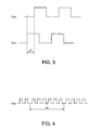
- This theoretical regulation circuit 46b activates the data-set-function-provided 1/2 frequency division circuit 43a for adjustment, thereby, as shown in FIG.
- the atomic oscillator 42 has excellent short-term accuracy (accuracy resulting from a temperature change observed in the oscillation frequency) and long-term stability (accuracy resulting from aging or others) compared with the quartz oscillator 41.
- the atomic oscillator is considerably high in power consumption compared with the quartz oscillator 41, if the atomic oscillator 42 is driven at all times, the duration of the battery 60 gets short.
- the oscillation section 40 is provided with an intermittent time management section (intermittent driving section) 47.
- This intermittent time management section 47 is so configured as to drive the atomic oscillator 42 in an intermittent manner with time intervals.
- the intermittent time management section 47 is provided with a counter 47a that counts the clock signal of the quartz oscillator 41, e.g., the clock signal of a predetermined frequency inside of the frequency division circuit 43 (the clock signal CL0 of 1Hz will also do). Every time the count value of this counter 47a reaches a value corresponding to the drive stop period (e.g., three hours), a power supply is made from the power supply section 13 only for the drive period (e.g., only ten seconds) to an intermittent to-be-driven section 49, which is configured by the atomic oscillator 42, the frequency division circuit 44, and the comparison circuit 45.
- a counter 47a that counts the clock signal of the quartz oscillator 41, e.g., the clock signal of a predetermined frequency inside of the frequency division circuit 43 (the clock signal CL0 of 1Hz will also do). Every time the count value of this counter 47a reaches a value corresponding to the drive stop period (e.g., three hours), a power supply is made from the power supply section 13
- the intermittent to-be-driven section 49 is driven only for ten seconds for every three hours, and during such driving, the comparison circuit 45 outputs the correction data D1 indicating the phase difference ⁇ F between the frequency division signal of the atomic oscillator 42 (the above-described 1Hz clock signal CL3) and the frequency division signal of the quartz oscillator 41 (the 1Hz comparison signal CL4).
- the correction section 46 updates the previous correction data D1 so that new correction data D1 is derived, and the correction data D1 being the update result is used as a basis to correct the phase of the clock signal CL0.
- FIG. 5 is a flowchart of the operation of the oscillation section 40.
- the intermittent time management section 47 resets the counter 47a so as to make it start counting the time (step S1), and based on the count value of the counter 47a, determines whether the drive stop period (three hours) has passed or not (step S2).
- the intermittent time management section 47 repeats the above determination-making of step S2 until the drive stop period (three hours) passes (step S2: n), and when a determination is made that the drive stop period (three hours) is now passed (step S2: y), a power supply is made to the intermittent to-be-driven section 49 including the atomic oscillator 42 so as to make the atomic oscillator 42 start oscillating (step S3).
- the comparison circuit 45 measures the phase difference ⁇ F between the frequency division signal of the atomic oscillator 42 (the above-described 1Hz clock signal CL3) and the frequency division signal of the quartz oscillator 41 (the 1Hz comparison signal CL4) (step S4).
- the correction data D1 is then forwarded to the correction section 46.
- the correction section 46 stores this correction data D1 into a predetermined area of the memory 46a, and when there is any previous correction data D1, this correction data is overwritten by the newly-acquired correction data D1 for update, and based on the resulting correction data D1, an amount of correction (amount of theoretical regulation) is calculated (step S5).
- the correction section 46 stores the amount of correction (amount of theoretical regulation) into the predetermined area of the memory 46a, and based on this amount of correction, the theoretical regulation circuit 46b goes through a process of activating the data-set-function-provided 1/2 frequency division circuit 43a for adjustment (step S6), thereby correcting the amount of phase shift observed in the 1Hz clock signal CL0 (the comparison signal CL4).
- the intermittent time management section 47 cuts off the power supply, and stops the operation of the intermittent-to-be-driven section 49. The procedure then goes to the process of step S1 (step S7).
- the amount of phase shift is corrected for the 1Hz clock signal CL0, and after three hours, when the intermittent to-be-driven section 49 is driven again, the process is repeated, i.e., the phase difference ⁇ F is newly measured between the frequency division signal of the atomic oscillator 42 and the frequency division signal of the quartz oscillator 41, and the amount of phase shift is corrected for the 1Hz clock signal CL0 in such a manner as to correct the phase difference ⁇ F.
- the quartz oscillator 41 is always driven, and the atomic oscillator 42 is driven in an intermittent manner. Every time the atomic oscillator 42 is driven, the amount of phase shift is measured for the 1Hz comparison signal CL4 being a frequency division signal of the quartz oscillator 41 with reference to the clock signal CL2 of the atomic oscillator 42. In such a manner as to correct this amount of phase shift, the 1Hz clock signal CL0 is corrected. As such, the accuracy of the clock signal CL0 can be increased in accuracy with reference to the atomic oscillator 42 while avoiding the increase of the entire power consumption by stopping the atomic oscillator 42 in an intermittent manner so that any possible error of a timepiece can be reduced.
- the quartz oscillator 41 before correction shows the negative frequency deviation during daytime hours with the temperature lower than a reference temperature (e.g., 25 degrees) TO as shown in FIG. 6(B), and during nighttime hours with the temperature higher than the reference temperature T0, the frequency deviation is changed to be positive.
- the quartz oscillator 41 is corrected with the accuracy of the atomic oscillator 42 for every three hours so that the absolute value of the frequency deviation becomes smaller as shown in FIG. 6(C).
- the area enclosed by the line of the reference temperature T0 (reference character ⁇ in the drawing) and the line of the frequency deviation (reference character ⁇ in the drawing) is equivalent to the error of a timepiece per day (error per day).
- the accuracy correction using the accuracy of the atomic oscillator 42 is performed at intervals (three hours) shorter than the daytime hours with the relatively high temperature in a day or than the nighttime hours with the relatively low temperature. This enables to cancel out the positive frequency deviation observed in the daytime hours and the negative frequency deviation observed in the nighttime hours so that the per-day error, the per-month error, and the per-year error of the wristwatch 10 can be reduced.
- the frequency deviation dependent on the temperature properties of the quartz oscillator 41 is 0.1 ppm
- eight-time correction-making a day can reduce the frequency deviation down to about 1/8, i.e., about 0.0125 ppm (equivalent to about an error of 0.4 seconds per year).
- the power consumption in the atomic oscillator 42 is of 0.1W, because the oscillator is driven only ten seconds for every three hours (10800 seconds), the power to be consumed by the atomic oscillator 42 can be suppressed to 10/10800, i.e., down to the power consumption of about 1/1000 (10 -4 W).
- the frequency deviation dependent on the aging properties of the quartz crystal is 0.2 ppm ( ⁇ in the drawing) in three years, in this embodiment, it is corrected to be almost the same as the long-term frequency deviation of the atomic oscillator 42, thereby deriving the frequency deviation of about 10 -4 ppm same as the accuracy of the atomic oscillator 42 ( ⁇ in the drawing).
- the resulting wristwatch 10 can be of high quality in which no error variation is observed for a long time after it is put in use.
- the wristwatch 1 can be sufficiently applied to a railway timepiece required to be high in accuracy for use by railway staff or train drivers of subways or others.
- a wristwatch 10A of a second embodiment is provided with a sensor section 65 as shown in FIG. 8, and this sensor section 65 includes a first detection section (reference oscillator influence information detection section) 70 detecting first information (reference oscillator influence information) that affects the operation of the quartz oscillator (reference oscillation section) 41 or others, and a second detection section (high-accuracy oscillator influence information detection section) 80 detecting second information (high-accuracy oscillator influence information) that affects the operation of the atomic oscillator (high-accuracy oscillator) 42 or others.
- first detection section reference oscillator influence information detection section
- first information reference oscillator influence information
- high-accuracy oscillator influence information detection section 80 detecting second information (high-accuracy oscillator influence information) that affects the operation of the atomic oscillator (high-accuracy oscillator) 42 or others.
- the first detection section 70 is provided with a temperature detection section 71 that detects the temperature (outside air temperature included), a voltage detection section 72 that detects the power supply voltage, and a posture detection section 73 that detects the posture of the wristwatch 10A.
- the temperature change is a factor of causing a frequency change of the quartz oscillator 41
- the reduction of the power supply voltage is a factor of causing the components in the wristwatch 10A to be unstable during operation
- the posture of the wristwatch 10A is a factor of causing the quartz oscillator 41 to vary in frequency, e.g., the posture of affecting the mechanical oscillation of the quartz crystal.
- the second detection section 80 is provided with a magnetic field detection section 81 that detects the magnetic field (changed magnetic flux) of the geomagnetism or others. Once exceeding an allowable level, the magnetic field becomes a factor of causing the atomic oscillator 42 to be unstable during operation.
- the intermittent time management section 47 inside of the oscillation section 40 sets the drive stop time ST of the atomic oscillator 42 in accordance with the aging properties ⁇ of the quartz crystal. More specifically, as shown in the same drawing, because the aging properties ⁇ of the quartz crystal are the properties that show a logarithmic change, by the intermittent time management section 47 changing the drive stop time ST of the atomic oscillator 42 in a logarithmic manner, the drive stop time is so set as to be the shortest immediately after the wristwatch 10 is put in use, and with a lapse of time, the drive stop time is so set as to be longer by degrees.
- FIG. 10 is a flowchart of the operation in this case. Note that this temporary correction process is a process to be continuously executed at predetermined interrupt intervals.
- the intermittent time management section 47 determines whether the voltage detected by the voltage detection section 72 is equal to or lower than a preset threshold value Z1 (step S11).
- a preset threshold value Z1 applied is a criterion value for a determination-making whether the remaining amount of battery is low or not.
- the intermittent time management section 47 sets the clock correction to be in a stop state in the quartz oscillator 41 (step S20).
- this stop state the oscillation section 40 does not drive the atomic oscillator 42 or perform clock correction even after the drive stop time ST is passed, thereby suppressing the power consumption, and keeping the drive time of the wristwatch 10A.
- the setting of this stop state is cleared when the voltage exceeds the threshold value Z1.
- step S11 when the voltage exceeds the threshold value Z1 (step S11: NO), the intermittent time management section 47 determines whether the magnetic field detected by the magnetic field detection section 81 exceeds a preset threshold value Z2 or not (step S12).
- step S12 YES
- the procedure also goes to the process of step S20, and the clock correction is set to be in the stop state.
- the threshold value Z2 applied is the allowance level of the magnetic field with respect to the atomic oscillator 42, thereby enabling to avoid a possible case of driving the atomic oscillator 42 when the generated magnetic field is of a level causing the atomic oscillator 42 to be unstable during operation.
- step S12 when the magnetic field is equal to or smaller than the threshold value Z2 (step S12: NO), the intermittent time management section 47 determines whether or not an amount of temperature change detected by the temperature detection section 71 per a predetermined time exceeds a preset threshold value Z3 (step S13).
- step S13 YES
- steps S3 to S7 in the below, referred to as clock correction process
- step S21 the processes of steps S3 to S7 (in the below, referred to as clock correction process) are executed (step S21), i.e., the intermittent to-be-driven section 49 including the atomic oscillator 42 is driven, and the clock signal CL0 coming from the quartz oscillator 41 is corrected.
- the threshold value Z3 applied is the allowance level of any frequency change dependent on the temperature of the quartz oscillator 41. This enables to execute the clock correction process when a frequency change exceeding the allowance level is observed, and to swiftly avoid any frequency drift possibly caused to the clock signal CL0 as a result of the frequency change caused by the temperature change occurred in
- step S13 determines whether or not the posture detected by the posture detection section 73 is a posture affecting the quartz oscillator 41, e.g., causing frequency change (step S14). If it affects the quarts oscillator 41 (step S14: YES), the clock correction process of step S21 is executed. This enables to swiftly avoid any possible frequency drift observed in the clock signal CL0 as a result of the frequency change caused by any posture change of the quartz oscillator 41. On the other hand, when the determination result of step S14 is a negative result, the intermittent time management section 47 terminates this process once, and goes through the process repeatedly.
- any information affecting the operation of the quartz oscillator 41 and that of the atomic oscillator 42 is monitored, and when any information possibly causing a frequency change to the quartz oscillator 41 (amount of temperature change, posture) is detected, the clock correction process is executed.
- the clock correction is stopped so that the clock signal CL0 can be quickly corrected in accordance with the frequency change observed in the quartz oscillator 41.
- the possible error of a timepiece can be reduced to a further extent.
- the drive stop time ST of the atomic oscillator 42 is so set as to be longer by degrees in accordance with the aging properties ⁇ of the quartz crystal. Therefore, in the first half of the period in which the quartz oscillator 41 shows a large frequency change due to aging (within substantially a half year after the timepiece is put in use as shown in FIG. 9), the clock correction process is executed at relatively short intervals, and in the second half of the period with a small frequency change by aging (substantially a half year and thereafter as shown in FIG. 9), the clock correction process is executed at relatively long intervals.
- This thus enables to reduce the frequency of driving the atomic oscillator 42 or others while suppressing any frequency change possibly caused by aging so that the power consumption can be reduced. Thanks thereto, compared with the first embodiment, the possible error of a timepiece can be reduced to a further extent, and the power consumption can be also reduced.
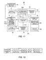
- a wristwatch 10B of a third embodiment is provided with a temperature detection section 71 detecting the temperature (reference oscillator influence information) as shown in FIG. 11, and this temperature detection section 71 is connected to the intermittent time management section 47 of the oscillation section 40.
- This intermittent time management section 47 is provided with a counter 47a1 for counting an update period P1 of correction data, and a counter 47b2 for counting the temperature detection interval P2.
- the intermittent time management section is so configured as to be able to count the update period P1 and the temperature detection interval P2.
- the degree may be roughly set such as for every five degrees. If this is the case, for correction data D1(n) of an intermediate temperature that is not set with the correction data, a complementary calculation process or others may be executed for specification using correction data D1 (m), D1 (m+1) (where m ⁇ n ⁇ m+1) for the preceding and subsequent temperatures, for example. Alternatively, in view of increasing the accuracy, the degree may be set precisely such as for every 0.5 degrees.
- FIG. 13 is a flowchart of the operation of the oscillation section 40.
- the intermittent time management section 47 sets 30 days for the update period P1 of the correction data D1 (k), and sets 10 minutes for the temperature detection interval P2 (step S31).
- the update period P1 is then started to be counted by the counter 47a1 (step S32), and a determination is made whether the update period P1 is now passed or not (step S33).
- step 533: YES the intermittent time management section 47 starts counting the update period P1 all over again, and when the update period P1 is not yet passed (step S33: NO), it starts counting the temperature detection interval P2 for temperature detection by the counter 47a2 (step S34), and waits until the temperature detection interval P2 passes (step S35).
- the intermittent time management section 47 measures the temperature T by the temperature detection section 71 (step S36), and then determines whether or not the measured temperature T is the temperature detected for the first time during the counting of the current update period P1 (step S37).
- the intermittent time management section 47 makes a power supply to the intermittent to-be-driven section 49 including the atomic oscillator 42, and makes the atomic oscillator 42 start oscillating (step S38). Thereafter, after the atomic oscillator 42 is driven in a stable manner, the intermittent time management section 47 uses the comparison circuit 45 to measure the phase difference ⁇ F between the frequency division signal of the atomic oscillator 42 (the above-described 1Hz clock signal CL3) and the frequency division signal of the quartz oscillator 41 (the 1Hz comparison signal CL4) (step S39), and calculates the amount of correction for use for correcting the phase difference ⁇ F (step S40).
- the intermittent time management section then rewrites correction data D1(T) corresponding to the above-described measured temperature T stored in the memory 46a by the correction section 46 to derive correction data corresponding to the calculated amount of correction (step S41), and cuts off the power supply to the intermittent to-be-driven section 49, thereby stopping the operation of the intermittent to-be-driven section 49 (step S42).
- the intermittent time management section 47 goes through a process of correcting the amount of phase shift observed in the clock signal CL0 (step S43), and the procedure goes to the process of step S33.
- the processes of steps S33 to S43 are then executed repeatedly.
- step S37 when the measured temperature T is not the temperature detected for the first time during the counting of the current update period P1 (step S37: YES), based on the correction data D1(T) corresponding to the measured temperature T stored in the memory 46a, the process of correcting the amount of phase shift is executed to the clock signal CL0 (step S43), and the procedure goes to the process of step S33.
- the processes of steps S33 to S43 are then executed repeatedly.
- the temperature T is measured in the temperature detection interval P2, and only when the resulting temperature T is the first-time-detected temperature, the intermittent to-be-driven section 49 including the atomic oscillator 42 is driven so that the correction data D1(T) corresponding to the measured temperature T is acquired.
- This thus enables to update the correction data D1(k) in the memory 46a to be the latest value.
- the correction data D1(k) in the memory 46a can be updated in accordance with the variation so that the clock signal CL0 can be protected from any possible frequency drift.
- the correction data D1(T) corresponding to the temperature T is acquired, and the correction data in the memory 46a is then updated. Accordingly, the correction data in the memory 46a can be updated appropriately in accordance with the frequency variation caused due to the aging properties of the quartz crystal or others so that any possible error of a timepiece can be reduced to a further extent.
- a temperature compensation system and an adjustment system are equipped inside of the quartz oscillator 41.
- This favorably eliminates any expensive device for adjustment use and adjustment work required for adjustment at the time of shipping.
- the adjustment can be completed only by putting the product in a high-temperature sink to go through any required temperature (e.g., -20 degrees to 70 degrees) at the time of shipping so that the adjustment work time can be shortened or the adjustment work can be simplified.
- the update period P1 is not necessarily fixed, and the update period P1 may be set variable. More preferably, the update period P1 may be set to be longer by degrees in accordance with the aging properties ⁇ of the quartz crystal (refer to FIG. 9). If the update period P1 is set variable in accordance with the aging properties ⁇ as such, it becomes possible to reduce the frequency of driving the atomic oscillator 42 or others while suppressing any possible frequency change caused by aging so that the power consumption can be reduced to a further extent. As such, with this configuration, the resulting oscillator can have the entire accuracy close to the accuracy of the atomic oscillator, and the power consumption of a level close to the power consumption in the quartz oscillator.
- the above-described embodiment is merely an example of the present invention, and it is understood that numerous other modifications can be arbitrarily devised without departing from the scope of the present invention.
- exemplified in the above second and third embodiments is the case of detecting the amount of temperature change and the posture as the information causing a frequency change to the quartz oscillator 41.
- This is surely not restrictive, and for example, an amount of humidity change may be detected, or as an alternative to the posture detection, the direction of gravity may be detected.
- the information causing the quartz oscillator 41 and the atomic oscillator 42 to be unstable during operation is not restrictive to the power supply voltage and the magnetic field, and any other information may be detected for the purpose.
- the second detection section 80 may be provided for detecting second information that affects the operation of the atomic oscillator 42 or others, and in the configuration, the atomic oscillator 42 may not be driven or the correction data may not be acquired while this second detection section 80 is detecting the second information.
- exemplified is the case of making a phase comparison between the quartz oscillator 41 and the atomic oscillator 42.
- a frequency comparison may be made between the quartz oscillator 41 and the atomic oscillator 42, and with reference to the frequency of the atomic oscillator 42, the oscillation frequency of the quartz oscillator 41 may be corrected.
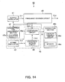
- FIG. 14 is a block diagram showing an exemplary configuration of the oscillation section 40 when the oscillation frequency is to be corrected.
- a quartz oscillator 41a is configured by a frequency adjustment section 41b configured by a series circuit of capacitors C1, C2, ... Cn, and switches SW1, SW2, ... SWn in parallel to a capacitor Cg, in addition to a crystal resonator X, an inverter INV1 for oscillation use, a feedback resistance Rf, a drive adjustment resistance Rd, a capacitor Cg on the gate side, and a capacitor Cd on the drain side.
- a correction section 46c is configured by the memory 46a, and a capacity variable circuit 46d that exercises control over the switches SW to SWn.
- the frequency division circuit 43b includes a no-data-set-function-provided 1/2 frequency division circuit as an alternative to the data-set-function-provided 1/2 frequency division circuit 43a, and this is the only difference.
- a comparison circuit 45a measures the cycle of a 1Hz comparison signal CL4 being a frequency division signal of the reference clock signal CL1 of the quartz oscillator 41 using the frequency division signal of 10 MHz of the atomic oscillator 42, for example, and outputs correction data D2 indicating this cycle to the correction section 46c. Based on this correction data D2, the correction section 46c then calculates the amount of the frequency drift observed in the quartz oscillator 41, and in accordance with the amount of frequency drift, the open/close state of the switches SW1 to SWn is controlled. As such, the quartz oscillator 41a is retained in the oscillation-frequency-changed state in such a manner that the frequency of the clock signal CL0 (comparison signal CL4) has the frequency of 1Hz.
- the oscillation frequency of the crystal oscillator 41a is updated with the frequency accuracy of the atomic oscillator 42, and in addition to the effects of the embodiments, the oscillation cycle of the clock signal CL0 can be almost constant as shown in FIG. 16 compared with the case with theoretical regulation of correcting the clock signal CL0 for every correction cycle TH (ten seconds).
- the above-described theoretical regulation may be used together with the capacity variable method of the quartz oscillator.
- the clock signal CL0 can be increased in adjustment amount.
- a capacitor for capacity change use is not necessarily provided in the quartz oscillation circuit, and the capacitor for capacity change use may be provided outside of the quartz oscillation circuit.
- exemplified is the case of correcting the amount of displacement observed in the clock signal CL0 through control over the phase or frequency of the reference clock signal CL1.
- the reference clock signal CL1 is not the only possibility, and any other signals (e.g. , frequency division signals) may be used for phase or frequency control as a reference use for generating the clock signal CL0 to correct the displacement amount of the clock signal CL0.
- the intermittent driving interval may be set not uniform, e.g., the drive stop period may be set shorter during daytime hours (e.g., two hours), and set longer during nighttime hours (e.g., four hours).
- a reference oscillator being a quartz oscillator using a fork-type crystal resonator
- an atomic oscillator being an oscillator (high-accuracy oscillator) whose accuracy is higher than that of the reference oscillator.
- the reference oscillator may be any other quartz oscillators including a temperature compensated crystal oscillator or others, a PLL (Phase Locked Loop) circuit, an CR oscillator or ceramic oscillator other than quartz oscillation, or an MEMS (Micro Electronic Mechanical Systems) oscillator being an integration of mechanical components and electronic circuits on a single silicon substrate.
- options include an oscillation circuit using an AT cut resonator in a range showing the higher frequency accuracy or frequency stability compared with the reference oscillator, a temperature compensated oscillator (TCXO), an oven controlled crystal oscillator (Oven Controlled Xtal Oscillator; OCXO), or others.
- TCXO temperature compensated oscillator
- Oven Controlled Xtal Oscillator Oven Controlled Xtal Oscillator
- the present invention is widely applicable to general timepieces and clocks, including a clock equipped with a calendar mechanism, a radio clock that receives radio waves with a time code superposed thereon, and corrects the time based on the time code, a in-pocket watch, a on-the-desk clock, a hanging clock, or others, or any electronic device that can be carried around, including a mobile phone, a PDA (Personal Digital Assistants) device, a portable measuring instrument, a mobile GPS (Global Positioning System), or others, or electric equipment including a standard oscillator, notebook personal computer, or others.
- the present invention is especially suitable to power-supply-equipped electronic devices that require long-term operation with a power supply section (battery) equipped for supply of the operating power.
- the time display can be made with sufficient accuracy even in the state of not being able to receive radio waves, e.g., in any place with no radio wave received (in buildings, in underground, in the water, close to a noise source), in any place with no radio wave (e.g., area with no standard frequency and time signal station, in outer space), with inappropriate antenna orientation, during radio wave routine check, with incorrect radio wave frequency or time code, in the weather state with low electric field intensity, or others.
- the resulting radio timepiece can provide high accuracy under various circumstances.
- a clock signal coming from the oscillation section 40 may be used as a criterion signal for determining a communications bit rate so that the communications can be performed at high speed with reliability.
- first detection section reference oscillator influence information detection section
- 72 temperature detection section
- 72 voltage detection section
- 73 posture detection section
- 80 second detection section (high-accuracy oscillator influence information detection section)
- 81 magnetic field detection section
- CL0 clock signal (output clock signal)
- CL1 reference clock signal
- CL2, CL3 clock signal
- CL4 comparison signal
- D1, D2 ... correction data P1 ... update period (correction data update period), P2 ... temperature detection interval
Landscapes
- Physics & Mathematics (AREA)
- General Physics & Mathematics (AREA)
- Electric Clocks (AREA)
- Stabilization Of Oscillater, Synchronisation, Frequency Synthesizers (AREA)
Abstract
Description
- The present invention relates to a clock signal output unit being equipped with a reference oscillator that generates a reference clock signal, and generating an output clock signal of a predetermined frequency from the reference clock signal for output, and a control method thereof, and an electronic device and a control method thereof.
- Conventionally, some type of an electronic clock generates a signal of 1Hz, for example, by frequency-dividing a reference clock signal coming from a reference oscillator, and counts the time based on this 1Hz signal. The electronic clock of such a type is well known by a annual rate timepiece, which implements an error of ± a few tens of seconds per year using a temperature compensated crystal oscillator for a reference oscillator (as an example, Patent Document 1). In recent years, a standard oscillator using an atomic oscillator is proposed (as examples,
Patent Documents 2 and 3) . - Patent Document 1:
JP-B-6-31731 - Patent Document 2:
United States Patent No. 6806784 - Patent Document 3:
United States Patent No. 6265945 - The issue here is that, in the conventional temperature compensated crystal oscillator, the temperature properties of a quartz crystal having the third-order properties are temperature-compensated by the temperature properties of a capacity having the second-order properties, thereby causing some temperature change to an oscillation frequency. Moreover, with the crystal oscillator of such a type, the aging properties of the quartz crystal causes some change to the oscillation frequency over the long terms, thereby resulting in poorer frequency accuracy compared with an atomic oscillator.
- On the other hand, if an atomic oscillator is to be used for a reference oscillator in an electronic clock, the duration of a battery is shortened because the power consumption of the atomic oscillator is higher compared with a quartz oscillator.
- The present invention is proposed in consideration of the above-described circumstances, and an object thereof is to provide a clock signal output unit that can increase the accuracy of a clock signal while avoiding the increase of the entire power consumption even with a high-accuracy oscillator relatively high in power consumption, and a control method thereof, and an electronic device and a control method thereof.
- In order to solve the above-described problems, the present invention is directed to a clock signal output unit being equipped with a reference oscillator that generates a reference clock signal, and generating, from the reference clock signal, an output clock signal of a predetermined frequency for output. The unit is characterized by including: a high-accuracy oscillator that generates a high-accuracy clock signal whose accuracy is higher than that of the reference oscillator; an intermittent driving section that drives the high-accuracy oscillator in an intermittent manner; and a correction section that acquires correction data for correcting an amount of displacement observed in the output clock signal with reference to the high-accuracy clock signal every time the high-accuracy oscillator is driven, and corrects the output clock signal based on the correction data.
- This configuration includes the high-accuracy oscillator that generates a high-accuracy clock signal whose accuracy is higher than that of the reference oscillator; the intermittent driving section that drives the high-accuracy oscillator in an intermittent manner; and the correction section that acquires correction data for correcting an amount of displacement observed in the output clock signal with reference to the high-accuracy clock signal every time the high-accuracy oscillator is driven, and corrects the output clock signal based on the correction data. Therefore, even if a high-accuracy oscillator with high power consumption is used, the output clock signal can be increased in accuracy with reference to the high-accuracy oscillator while avoiding the increase of the entire power consumption by stopping the high-accuracy oscillator in an intermittent manner.
- In the above configuration, a reference oscillator influence information detection section is provided for detecting reference oscillator influence information affecting the operation of the reference oscillator. When the reference oscillator influence information is detected, it is preferable that the intermittent driving section drives the high-accuracy oscillator, and the correction section acquires the correction data.
- With this configuration, when the reference oscillator influence information affecting the operation of the reference oscillator is detected, the high-accuracy oscillator is driven to acquire the correction data. This enables to quickly correct any frequency change caused by the reference oscillator influence information so that the accuracy of the output clock signal can be increased to a further extent.
- Alternatively, the above configuration includes a reference oscillator influence information detection section that detects reference oscillator influence information affecting the operation of the reference oscillator; and a storage section that stores therein the correction data corresponding to the reference oscillator influence information on a value basis. When the reference oscillator influence information is detected, and when the detected reference oscillator influence information is a first-time-detected value, it is preferable that the intermittent driving section drives the high-accuracy oscillator, the correction section acquires the correction data, the correction data is stored in the storage section, and the output clock signal is corrected based on this correction data, and when the detected reference oscillator influence information is not the first-time-detected value, it is preferable to correct the output clock signal based on the correction data corresponding to the value of the reference oscillator influence information stored in the storage section. With this configuration, because the high-accuracy oscillator is driven only when the detected reference oscillator influence information is a first-time-detected value, the frequency of driving the high-accuracy oscillator can be reduced so that the power consumption can be reduced.
- In the above configuration, when the detected reference oscillator influence information is a value detected for the first time in a predetermined correction data update period, it is preferable that the intermittent driving section drives the high-accuracy oscillator, and when the detected reference oscillator influence information is not the value detected for the first time in the correction data update period, the high-accuracy oscillator is kept in a no-drive state.
- With this configuration, when the detected reference oscillator influence information is not a value detected for the first time in the correction data update period, the high-accuracy oscillator is kept in a no-drive state so that the power consumption can be favorably reduced. In addition thereto, when the detected reference oscillator influence information is a value detected for the first time in the correction data update period, the high-accuracy oscillator is driven so that correction data in storage can be updated with any new correction data every time the correction data update period passes. This enables to update the correction data in accordance with any frequency change caused due to the aging properties or others of the reference oscillator so that the accuracy of the output clock signal can be increased to a further extent.
- In the above configuration, it is preferable that the reference oscillator influence information includes at least any one of an amount of temperature change, an amount of humidity change, an electric power supply, a posture or a gravity direction of the clock signal output unit.
- Alternatively, the above configuration includes a high-accuracy oscillator influence information detection section that detects high-accuracy oscillator influence information affecting the operation of the high-accuracy oscillator. During the detection of the high-accuracy oscillator influence information, it is preferable that the high-accuracy oscillator is kept in the no-drive state. With this configuration, during the detection of the high-accuracy oscillator influence information affecting the operation of the high-accuracy oscillator, the high-accuracy oscillator is kept in the no-drive state so that a possible case of driving the high-accuracy oscillator in the operation-unstable state can be avoided. Moreover, in the above configuration, it is preferable that the high-accuracy oscillator influence information includes at least either a magnetic field or an electric power supply.
- In the above configuration, it is preferable that the reference oscillator is small in power consumption compared with the high-accuracy oscillator, and the reference oscillator may be a quartz oscillator, a CR oscillator, or a MEMS oscillator. Moreover, the high-accuracy clock signal may be a signal whose frequency is higher than that of the reference clock signal, and the high-accuracy oscillator may be any one of an atomic oscillator, a temperature compensated oscillator, an oven controlled crystal oscillator, and an oscillator using an AT cut resonator.
- The above configuration may include, alternatively, a comparison section that makes a phase comparison or a frequency comparison between the reference clock signal and the high-accuracy clock signal, and the intermittent driving section may drive the comparison section only during driving the high-accuracy oscillator so as to reduce the power consumption to a further extent.
- Further, in the above configuration, the intermittent driving section may gradually lengthen an intermittent driving interval in accordance with the aging properties of the reference oscillator. This configuration enables to reduce the frequency of driving the high-accuracy oscillator while suppressing a frequency change possibly caused by aging so that the power consumption can be reduced.
- The present invention is directed also to a control method of a clock signal output unit being equipped with a reference oscillator that generates a reference clock signal, and generating, from the reference clock signal, an output clock signal of a predetermined frequency for output. The method is characterized in that a high-accuracy oscillator that generates a high-accuracy clock signal whose accuracy is higher than that of the reference oscillator is driven in an intermittent manner, and every time the high-accuracy oscillator is driven, correction data is acquired for use for correcting an amount of displacement observed in the output clock signal with reference to the high-accuracy clock signal, and based on the correction data, the output clock signal is corrected.
- With this configuration, the high-accuracy oscillator that generates a high-accuracy clock signal whose accuracy is higher than that of the reference oscillator is driven in an intermittent manner, and every time the high-accuracy oscillator is driven, correction data is acquired for use for correcting an amount of displacement observed in the output clock signal with reference to the high-accuracy clock signal, and based on the correction data, the output clock signal is corrected. Therefore, even if a high-accuracy oscillator with high power consumption is used, the output clock signal can be increased in accuracy while avoiding the increase of the entire power consumption.
- The present invention is directed also to an electronic device equipped with a clock signal output section that generates, from a reference clock signal coming from a reference oscillator, an output clock signal of a predetermined frequency for output. The device is
characterized by including: a high-accuracy oscillator that generates a high-accuracy clock signal whose accuracy is higher than that of the reference oscillator; an intermittent driving section that drives the high-accuracy oscillator in an intermittent manner; and a correction section that acquires correction data for correcting an amount of displacement observed in the output clock signal with reference to the high-accuracy clock signal every time the high-accuracy oscillator is driven, and corrects the output clock signal based on the correction data. - This configuration includes the high-accuracy oscillator that generates a high-accuracy clock signal whose accuracy is higher than that of the reference oscillator, the intermittent driving section that drives the high-accuracy oscillator in an intermittent manner, and the correction section that acquires correction data for correcting an amount of displacement observed in the output clock signal with reference to the high-accuracy clock signal every time the high-accuracy oscillator is driven, and corrects the output clock signal based on the correction data. Therefore, even if a high-accuracy oscillator with high power consumption is used, the output clock signal can be increased in accuracy while avoiding the increase of the entire power consumption.
- Alternatively, in the above configuration, the electronic device may be configured as a timepiece including a time display section that displays thereon a time based on the output clock signal. The electronic device preferably includes therein a power supply section that supplies an operating power to the electronic device. This configuration enables the long-term operation even with an electronic device equipped therein with a power supply section.
- The present invention is directed also to a control method of an electronic device equipped with a clock signal output section that generates, for output, an output clock signal of a predetermined frequency from a reference clock signal coming from a reference oscillator. The method is characterized in that a high-accuracy oscillator generating a high-accuracy clock signal whose accuracy is higher than that of the reference oscillator is driven in an intermittent manner, and every time the high-accuracy oscillator is driven, correction data for correcting an amount of displacement observed in the output clock signal is acquired with reference to the high-accuracy clock signal, and the output clock signal is corrected based on the correction data.
- In this configuration, the high-accuracy oscillator generating a high-accuracy clock signal whose accuracy is higher than that of the reference oscillator is driven in an intermittent manner, and every time the high-accuracy oscillator is driven, correction data for correcting an amount of displacement observed in the output clock signal is acquired with reference to the high-accuracy clock signal, and the output clock signal is corrected based on the correction data. Therefore, even if a high-accuracy oscillator with high power consumption is used, the output clock signal can be increased in accuracy while avoiding the increase of the entire power consumption.
- The present invention includes a high-accuracy oscillator that generates a high-accuracy clock signal whose accuracy is higher than that of the reference oscillator; an intermittent driving section that drives the high-accuracy oscillator in an intermittent manner; and a correction section that acquires correction data for correcting an amount of displacement observed in the output clock signal with reference to the high-accuracy clock signal every time the high-accuracy oscillator is driven, and corrects the output clock signal based on the correction data. Therefore, even if a high-accuracy oscillator with high power consumption is used, the output clock signal can be increased in accuracy with reference to the high-accuracy oscillator while avoiding the increase of the entire power consumption by stopping this high-accuracy oscillator in an intermittent manner.
- Further, with the present invention, when the reference oscillator influence information affecting the operation of the reference oscillator is detected, the high-accuracy oscillator is driven to acquire the correction data. This enables to quickly correct any frequency change caused by the reference oscillator influence information so that the accuracy of the output clock signal can be increased to a further extent.
- Still further, with the present invention, when the detected reference oscillator influence information is a value detected for the first time in a predetermined correction data update period, the high-accuracy oscillator is driven, and when the detected reference oscillator influence information is not the value detected for the first time in the correction data update period, the high-accuracy oscillator is kept in a no-drive state. Therefore, the frequency of driving the high-accuracy oscillator is reduced, and the power consumption can be thus reduced. In this case, every time the correction data update period is passed, the high-accuracy oscillator is driven so that any new correction data is acquired, and the correction data can be updated in accordance with a frequency change caused due to the aging properties or others of the reference oscillator. The output clock signal can be thus increased in accuracy to a further extent.
- In the above configuration, while the high-accuracy oscillator influence information affecting the operation of the high-accuracy oscillator is detected, the high-accuracy oscillator is kept in the no-drive state. This thus avoids the case of driving the high-accuracy oscillator in the operation-unstable state.
- In the below, an embodiment of the present invention is described by referring to the drawings.
- FIG. 1 is a block diagram showing the configuration of a wristwatch of an embodiment of the present invention. This wristwatch (electronic timepiece) 10 is configured to include a
hand movement mechanism 11 and adrive section 12 both configuring a timepiece module, and apower supply section 13 that supplies an operating power to this timepiece module. - The
hand movement mechanism 11 configures a time display section that displays thereon the time by driving asecond hand 21, aminute hand 22, and anhour hand 23, and as shown in the drawing, includes agear train 29 in which asecond wheel 24, asecond wheel 25, and atube wheel 26 are coupled together viaintermediate wheels second wheel 24 is attached with one end of thesecond hand 21, the rotation axis of thesecond wheel 25 is attached with one end of theminute hand 22, and the rotation axis of thetube wheel 26 is attached with one end of thehour hand 23. Thesecond wheel 24 is meshed with adrive gear 31 of adrive motor 30, and thesecond wheel 24 is rotate-driven in response to the rotation of thedrive motor 30. This rotation is transferred to thesecond wheel 25 and thetube wheel 26 so that thesecond hand 21, theminute hand 22, and thehour hand 23 are each rotate-driven. By thesehands 21 to 23, the time is displayed. - The
drive section 12 is provided with an oscillation section (clock signal output section) 40 and amotor drive section 50. Theoscillation section 40 outputs a 1Hz clock signal (output clock signal) CL0, and based on this 1Hz clock signal CL0, themotor drive section 50 supplies a drive pulse to thedrive motor 30, thereby driving thedrive motor 30. Note here that thiswristwatch 1 may be provided with a liquid crystal display device as an alternative to thehand movement mechanism 11 or in addition to thehand movement mechanism 11, and the liquid crystal display device may be so configured as to display thereon the time. If this is the case, thedrive section 12 may be provided with a counter for use with a timepiece, counting the 1Hz clock signal CL0, and a liquid crystal drive section that drives the liquid crystal display device based on the count value of the counter for use with a timepiece. - The
power supply section 13 is configured to include abattery 60 disposed inside of thiswristwatch 10, and a constant voltage circuit (not shown) that converts the power stored in thebattery 60 into a constant voltage for supply to the components of thedrive section 12. To thisbattery 60, applied is a coin-shaped primary battery such as lithium battery or silver battery. Note that thiswristwatch 10 may be provided therein with a power generation section such as solar panel, and with this being the case, a secondary battery is applied to thebattery 60. - In this embodiment, as shown in FIG. 2, the
oscillation section 40 is provided with a quartz oscillator (reference oscillation section) 41, and an atomic oscillator (high-accuracy oscillator) 42. Thequartz oscillator 41 is an oscillator that oscillates a fork-type crystal resonator, and outputs a reference clock signal CL1 of 32.768 kHz, for example. To theatomic oscillator 42, applied is a cesium atomic oscillator whose frequency accuracy and the frequency stability are higher than those of thequartz oscillator 41, e.g., an oscillator that outputs a clock signal CL2 of 9.2 GHz. The cesium atomic oscillator is not restrictive, and any other atomic oscillator (e.g., rubidium atomic oscillator) may be used. Thequartz oscillator 41 may be any arbitrary quartz oscillator such as oscillator to be used in a annual rate timepiece or in a daily rate timepiece. - The
oscillation section 40 is provided with afrequency division circuit 43 that frequency-divides the reference clock signal CL1 of thequartz oscillator 41. Thisfrequency division circuit 43 is configured to include a plurality of frequency dividers that are connected in multistage, including a data-set-function-provided 1/2frequency division circuit 43a serving as an adjustment amount provision section. The frequency division circuit frequency-divides the reference clock signal CL1 to derive 1Hz, and outputs the 1Hz clock signal CL0. This clock signal CL0 is output to the outside as an output of theoscillation section 40, and is also output to acomparison circuit 45 inside of theoscillation section 40 as a comparison signal CL4. - The
oscillation section 40 is provided with afrequency division circuit 44 that frequency-divides the clock signal CL2 of theatomic oscillator 42. Thefrequency division circuit 44 frequency-divides the clock signal CL2 to derive 1Hz, and outputs the resulting 1Hz frequency division signal CL3 to thecomparison circuit 45. - The
comparison circuit 45 is a circuit that takes charge of making a phase comparison between the 1Hz comparison signal CL4 being a frequency division signal of the reference clock signal CL1 of thequartz oscillator 41, and the 1Hz clock signal CL3 being a frequency division signal of the clock signal CL2 of theatomic oscillator 42. To be specific, as shown in FIG. 3, the rise timing is measured for both the comparison signal CL4 and the clock signal CL3 using the frequency division signal of the atomic oscillator 42 (the clock signal acquired from any of the frequency-division stages of thefrequency division circuit 44, e.g., signal of 100 Hz), thereby outputting, to acorrection section 46, correction data D1 indicating a phase difference ΔF of the comparison signal CL4 with respect to the clock signal CL2. - Note here that it is also possible to measure the phase difference ΔF between the comparison signal CL4 and the clock signal CL3 using the 9.2 GHz clock signal CL2 of the
atomic oscillator 42. In view of reducing the power consumption, however, it is considered preferable to reduce the high-frequency-configured network using, for measurement, a frequency division signal of the clock signal CL2 of theatomic oscillator 42. The comparison signal CL4 for input to thecomparison circuit 45 does not necessarily have the cycle of the output clock signal, and may have the intermediate frequency of frequency division if sharing the same design frequency with the clock signal CL3, e.g., 16 Hz. - The
correction section 46 is a circuit for correcting the clock signal CL0 based on the correction data D1 acquired from thecomparison circuit 45. As shown in FIG. 2, the circuit is configured to include amemory 46a that stores therein the correction data D1 or others, and atheoretical regulation circuit 46b that transmits an adjustment timing signal T1 to the data-set-function-provided 1/2frequency division circuit 43a for activation thereof for adjustment. Thistheoretical regulation circuit 46b activates the data-set-function-provided 1/2frequency division circuit 43a for adjustment, thereby, as shown in FIG. 4, extending the clock signal CL0 by any needed phase amount (adjustment amount) for every correction period (ten seconds) TH, and correcting the phase of the clock signal CL0 by an amount of phase shift with respect to the clock signal CL2 (corresponding to the phase difference ΔF). - The issue here is that the
atomic oscillator 42 has excellent short-term accuracy (accuracy resulting from a temperature change observed in the oscillation frequency) and long-term stability (accuracy resulting from aging or others) compared with thequartz oscillator 41. On the other hand, because the atomic oscillator is considerably high in power consumption compared with thequartz oscillator 41, if theatomic oscillator 42 is driven at all times, the duration of thebattery 60 gets short. - In consideration thereof, in this embodiment, as shown in FIG. 2, the
oscillation section 40 is provided with an intermittent time management section (intermittent driving section) 47. This intermittenttime management section 47 is so configured as to drive theatomic oscillator 42 in an intermittent manner with time intervals. - The intermittent
time management section 47 is provided with acounter 47a that counts the clock signal of thequartz oscillator 41, e.g., the clock signal of a predetermined frequency inside of the frequency division circuit 43 (the clock signal CL0 of 1Hz will also do). Every time the count value of thiscounter 47a reaches a value corresponding to the drive stop period (e.g., three hours), a power supply is made from thepower supply section 13 only for the drive period (e.g., only ten seconds) to an intermittent to-be-driven section 49, which is configured by theatomic oscillator 42, thefrequency division circuit 44, and thecomparison circuit 45. As a result, the intermittent to-be-driven section 49 is driven only for ten seconds for every three hours, and during such driving, thecomparison circuit 45 outputs the correction data D1 indicating the phase difference ΔF between the frequency division signal of the atomic oscillator 42 (the above-described 1Hz clock signal CL3) and the frequency division signal of the quartz oscillator 41 (the 1Hz comparison signal CL4). After acquiring the correction data D1, thecorrection section 46 updates the previous correction data D1 so that new correction data D1 is derived, and the correction data D1 being the update result is used as a basis to correct the phase of the clock signal CL0. - FIG. 5 is a flowchart of the operation of the
oscillation section 40. - In the
oscillation section 40, the intermittenttime management section 47 resets thecounter 47a so as to make it start counting the time (step S1), and based on the count value of thecounter 47a, determines whether the drive stop period (three hours) has passed or not (step S2). The intermittenttime management section 47 repeats the above determination-making of step S2 until the drive stop period (three hours) passes (step S2: n), and when a determination is made that the drive stop period (three hours) is now passed (step S2: y), a power supply is made to the intermittent to-be-driven section 49 including theatomic oscillator 42 so as to make theatomic oscillator 42 start oscillating (step S3). - Thereafter, after the oscillation frequency of the
atomic oscillator 42 is stabilized, thecomparison circuit 45 measures the phase difference ΔF between the frequency division signal of the atomic oscillator 42 (the above-described 1Hz clock signal CL3) and the frequency division signal of the quartz oscillator 41 (the 1Hz comparison signal CL4) (step S4). The correction data D1 is then forwarded to thecorrection section 46. Thecorrection section 46 then stores this correction data D1 into a predetermined area of thememory 46a, and when there is any previous correction data D1, this correction data is overwritten by the newly-acquired correction data D1 for update, and based on the resulting correction data D1, an amount of correction (amount of theoretical regulation) is calculated (step S5). - Next, the
correction section 46 stores the amount of correction (amount of theoretical regulation) into the predetermined area of thememory 46a, and based on this amount of correction, thetheoretical regulation circuit 46b goes through a process of activating the data-set-function-provided 1/2frequency division circuit 43a for adjustment (step S6), thereby correcting the amount of phase shift observed in the 1Hz clock signal CL0 (the comparison signal CL4). Moreover, when the drive period (ten seconds) is passed after the power supply is started to the intermittent to-be-driven section 49 including theatomic oscillator 42, the intermittenttime management section 47 cuts off the power supply, and stops the operation of the intermittent-to-be-driven section 49. The procedure then goes to the process of step S1 (step S7). In this manner, while the intermittent to-be-driven section 49 is not in operation, based on the amount of correction stored in thememory 46a (amount of theoretical regulation), the amount of phase shift is corrected for the 1Hz clock signal CL0, and after three hours, when the intermittent to-be-driven section 49 is driven again, the process is repeated, i.e., the phase difference ΔF is newly measured between the frequency division signal of theatomic oscillator 42 and the frequency division signal of thequartz oscillator 41, and the amount of phase shift is corrected for the 1Hz clock signal CL0 in such a manner as to correct the phase difference ΔF. - With the configuration above, when the
wristwatch 1 is being driven, thequartz oscillator 41 is always driven, and theatomic oscillator 42 is driven in an intermittent manner. Every time theatomic oscillator 42 is driven, the amount of phase shift is measured for the 1Hz comparison signal CL4 being a frequency division signal of thequartz oscillator 41 with reference to the clock signal CL2 of theatomic oscillator 42. In such a manner as to correct this amount of phase shift, the 1Hz clock signal CL0 is corrected. As such, the accuracy of the clock signal CL0 can be increased in accuracy with reference to theatomic oscillator 42 while avoiding the increase of the entire power consumption by stopping theatomic oscillator 42 in an intermittent manner so that any possible error of a timepiece can be reduced. - To be specific, when the temperature varies in a day as shown in FIG. 6 (A), the
quartz oscillator 41 before correction shows the negative frequency deviation during daytime hours with the temperature lower than a reference temperature (e.g., 25 degrees) TO as shown in FIG. 6(B), and during nighttime hours with the temperature higher than the reference temperature T0, the frequency deviation is changed to be positive. With this configuration, thequartz oscillator 41 is corrected with the accuracy of theatomic oscillator 42 for every three hours so that the absolute value of the frequency deviation becomes smaller as shown in FIG. 6(C). - In FIG. 6(C), the area enclosed by the line of the reference temperature T0 (reference character α in the drawing) and the line of the frequency deviation (reference character β in the drawing) is equivalent to the error of a timepiece per day (error per day). In this embodiment, the accuracy correction using the accuracy of the
atomic oscillator 42 is performed at intervals (three hours) shorter than the daytime hours with the relatively high temperature in a day or than the nighttime hours with the relatively low temperature. This enables to cancel out the positive frequency deviation observed in the daytime hours and the negative frequency deviation observed in the nighttime hours so that the per-day error, the per-month error, and the per-year error of thewristwatch 10 can be reduced. When the frequency deviation dependent on the temperature properties of thequartz oscillator 41 is 0.1 ppm, for example, eight-time correction-making a day can reduce the frequency deviation down to about 1/8, i.e., about 0.0125 ppm (equivalent to about an error of 0.4 seconds per year). Moreover, when the power consumption in theatomic oscillator 42 is of 0.1W, because the oscillator is driven only ten seconds for every three hours (10800 seconds), the power to be consumed by theatomic oscillator 42 can be suppressed to 10/10800, i.e., down to the power consumption of about 1/1000 (10-4W). - Further, as shown in FIG. 7, when the frequency deviation dependent on the aging properties of the quartz crystal is 0.2 ppm (γ in the drawing) in three years, in this embodiment, it is corrected to be almost the same as the long-term frequency deviation of the
atomic oscillator 42, thereby deriving the frequency deviation of about 10-4 ppm same as the accuracy of the atomic oscillator 42 (θ in the drawing). As such, the resultingwristwatch 10 can be of high quality in which no error variation is observed for a long time after it is put in use. Moreover, with this configuration, not only theatomic oscillator 42 but also thefrequency division circuit 44 and thecomparison circuit 45 are stopped in an intermittent manner, whereby the power consumption can be reduced to a further extent, and even if a battery same as that in any conventional timepiece is used, the duration of the battery is not reduced that much. As such, in this configuration, even if theatomic oscillator 42 high in power consumption is used, any possible error of a timepiece can be reduced over a long time while avoiding the increase of the power consumption. Therefore, thewristwatch 1 can be sufficiently applied to a railway timepiece required to be high in accuracy for use by railway staff or train drivers of subways or others. - A
wristwatch 10A of a second embodiment is provided with asensor section 65 as shown in FIG. 8, and thissensor section 65 includes a first detection section (reference oscillator influence information detection section) 70 detecting first information (reference oscillator influence information) that affects the operation of the quartz oscillator (reference oscillation section) 41 or others, and a second detection section (high-accuracy oscillator influence information detection section) 80 detecting second information (high-accuracy oscillator influence information) that affects the operation of the atomic oscillator (high-accuracy oscillator) 42 or others. In the below, any component similar to that of the first embodiment is provided with the same reference numeral, and not described again in detail but only any different part will be described in detail. - The
first detection section 70 is provided with atemperature detection section 71 that detects the temperature (outside air temperature included), avoltage detection section 72 that detects the power supply voltage, and aposture detection section 73 that detects the posture of thewristwatch 10A. Here, the temperature change is a factor of causing a frequency change of thequartz oscillator 41, the reduction of the power supply voltage is a factor of causing the components in thewristwatch 10A to be unstable during operation, and the posture of thewristwatch 10A is a factor of causing thequartz oscillator 41 to vary in frequency, e.g., the posture of affecting the mechanical oscillation of the quartz crystal. - The
second detection section 80 is provided with a magneticfield detection section 81 that detects the magnetic field (changed magnetic flux) of the geomagnetism or others. Once exceeding an allowable level, the magnetic field becomes a factor of causing theatomic oscillator 42 to be unstable during operation. - Moreover, in this embodiment, as shown in FIG. 9, the intermittent
time management section 47 inside of theoscillation section 40 sets the drive stop time ST of theatomic oscillator 42 in accordance with the aging properties γ of the quartz crystal. More specifically, as shown in the same drawing, because the aging properties γ of the quartz crystal are the properties that show a logarithmic change, by the intermittenttime management section 47 changing the drive stop time ST of theatomic oscillator 42 in a logarithmic manner, the drive stop time is so set as to be the shortest immediately after thewristwatch 10 is put in use, and with a lapse of time, the drive stop time is so set as to be longer by degrees. Note that, in the drawing, exemplified is the case of changing the drive stop time ST every time the frequency deviation of the quartz crystal shows a change by a fixed amount, but the timing for such a change can be arbitrarily set, e.g., the drive stop time ST is changed every time a fixed length of time passes. - In the
wristwatch 10A, in addition to a routine correction process of subjecting thequartz oscillator 41 to clock correction by theoscillator section 40 driving theatomic oscillator 42 based on the drive stop time ST set by the intermittenttime management section 47, executed is a temporary correction process of correcting or stopping, for correction, the clock of thequartz oscillator 41 based on the detection result derived by the above-describedsensor section 65. - In the below, this temporary correction process is described. FIG. 10 is a flowchart of the operation in this case. Note that this temporary correction process is a process to be continuously executed at predetermined interrupt intervals.
- In the
oscillation section 40, first of all, the intermittenttime management section 47 determines whether the voltage detected by thevoltage detection section 72 is equal to or lower than a preset threshold value Z1 (step S11). Here, to this threshold value Z1, applied is a criterion value for a determination-making whether the remaining amount of battery is low or not. - When the voltage is equal to or lower than the threshold value Z1 (step S11: YES), for the aim of avoiding the possible power consumption needed to drive the
atomic oscillator 42 or others, the intermittenttime management section 47 sets the clock correction to be in a stop state in the quartz oscillator 41 (step S20). In the case with this stop state, theoscillation section 40 does not drive theatomic oscillator 42 or perform clock correction even after the drive stop time ST is passed, thereby suppressing the power consumption, and keeping the drive time of thewristwatch 10A. Herein, the setting of this stop state is cleared when the voltage exceeds the threshold value Z1. - On the other hand, when the voltage exceeds the threshold value Z1 (step S11: NO), the intermittent
time management section 47 determines whether the magnetic field detected by the magneticfield detection section 81 exceeds a preset threshold value Z2 or not (step S12). When the magnetic field exceeds the threshold value Z2 (step S12: YES), the procedure also goes to the process of step S20, and the clock correction is set to be in the stop state. Here, to the threshold value Z2, applied is the allowance level of the magnetic field with respect to theatomic oscillator 42, thereby enabling to avoid a possible case of driving theatomic oscillator 42 when the generated magnetic field is of a level causing theatomic oscillator 42 to be unstable during operation. - Next, when the magnetic field is equal to or smaller than the threshold value Z2 (step S12: NO), the intermittent
time management section 47 determines whether or not an amount of temperature change detected by thetemperature detection section 71 per a predetermined time exceeds a preset threshold value Z3 (step S13). When the amount exceeds the value (step S13: YES), the processes of steps S3 to S7 (in the below, referred to as clock correction process) are executed (step S21), i.e., the intermittent to-be-driven section 49 including theatomic oscillator 42 is driven, and the clock signal CL0 coming from thequartz oscillator 41 is corrected. Here, to the threshold value Z3, applied is the allowance level of any frequency change dependent on the temperature of thequartz oscillator 41. This enables to execute the clock correction process when a frequency change exceeding the allowance level is observed, and to swiftly avoid any frequency drift possibly caused to the clock signal CL0 as a result of the frequency change caused by the temperature change occurred in thequartz oscillator 41. - Moreover, when the amount of temperature change is equal to or smaller than the threshold value Z3 (step S13: NO), the intermittent
time management section 47 determines whether or not the posture detected by theposture detection section 73 is a posture affecting thequartz oscillator 41, e.g., causing frequency change (step S14). If it affects the quarts oscillator 41 (step S14: YES), the clock correction process of step S21 is executed. This enables to swiftly avoid any possible frequency drift observed in the clock signal CL0 as a result of the frequency change caused by any posture change of thequartz oscillator 41. On the other hand, when the determination result of step S14 is a negative result, the intermittenttime management section 47 terminates this process once, and goes through the process repeatedly. - As described in the foregoing, with this configuration, any information affecting the operation of the
quartz oscillator 41 and that of theatomic oscillator 42 is monitored, and when any information possibly causing a frequency change to the quartz oscillator 41 (amount of temperature change, posture) is detected, the clock correction process is executed. When any information possibly causing thequartz oscillator 41 and theatomic oscillator 42 to be unstable during the operation (power supply voltage, magnetic field) is detected, the clock correction is stopped so that the clock signal CL0 can be quickly corrected in accordance with the frequency change observed in thequartz oscillator 41. As such, compared with that of the first embodiment, the possible error of a timepiece can be reduced to a further extent. - What is more, with this configuration, the drive stop time ST of the
atomic oscillator 42 is so set as to be longer by degrees in accordance with the aging properties γ of the quartz crystal. Therefore, in the first half of the period in which thequartz oscillator 41 shows a large frequency change due to aging (within substantially a half year after the timepiece is put in use as shown in FIG. 9), the clock correction process is executed at relatively short intervals, and in the second half of the period with a small frequency change by aging (substantially a half year and thereafter as shown in FIG. 9), the clock correction process is executed at relatively long intervals. This thus enables to reduce the frequency of driving theatomic oscillator 42 or others while suppressing any frequency change possibly caused by aging so that the power consumption can be reduced. Thanks thereto, compared with the first embodiment, the possible error of a timepiece can be reduced to a further extent, and the power consumption can be also reduced. - A wristwatch 10B of a third embodiment is provided with a
temperature detection section 71 detecting the temperature (reference oscillator influence information) as shown in FIG. 11, and thistemperature detection section 71 is connected to the intermittenttime management section 47 of theoscillation section 40. This intermittenttime management section 47 is provided with a counter 47a1 for counting an update period P1 of correction data, and a counter 47b2 for counting the temperature detection interval P2. The intermittent time management section is so configured as to be able to count the update period P1 and the temperature detection interval P2. - As shown in FIG. 12, the
memory 46a carries therein correction data D1 (k) (K = temperature) corresponding to each temperature. Note that, in this drawing, exemplified is a case that the correction data D1 (k) is set for every degree, but in view of reducing the amount of data, the degree may be roughly set such as for every five degrees. If this is the case, for correction data D1(n) of an intermediate temperature that is not set with the correction data, a complementary calculation process or others may be executed for specification using correction data D1 (m), D1 (m+1) (where m<n<m+1) for the preceding and subsequent temperatures, for example. Alternatively, in view of increasing the accuracy, the degree may be set precisely such as for every 0.5 degrees. - FIG. 13 is a flowchart of the operation of the
oscillation section 40. - First of all, the intermittent
time management section 47 sets 30 days for the update period P1 of the correction data D1 (k), and sets 10 minutes for the temperature detection interval P2 (step S31). The update period P1 is then started to be counted by the counter 47a1 (step S32), and a determination is made whether the update period P1 is now passed or not (step S33). - When the update period P1 is passed (step 533: YES), the intermittent
time management section 47 starts counting the update period P1 all over again, and when the update period P1 is not yet passed (step S33: NO), it starts counting the temperature detection interval P2 for temperature detection by the counter 47a2 (step S34), and waits until the temperature detection interval P2 passes (step S35). - After the temperature detection interval P2 is passed (step S35: YES), the intermittent
time management section 47 measures the temperature T by the temperature detection section 71 (step S36), and then determines whether or not the measured temperature T is the temperature detected for the first time during the counting of the current update period P1 (step S37). - Here, if it is the first-time-detected temperature (step S37: NO), the intermittent
time management section 47 makes a power supply to the intermittent to-be-driven section 49 including theatomic oscillator 42, and makes theatomic oscillator 42 start oscillating (step S38). Thereafter, after theatomic oscillator 42 is driven in a stable manner, the intermittenttime management section 47 uses thecomparison circuit 45 to measure the phase difference ΔF between the frequency division signal of the atomic oscillator 42 (the above-described 1Hz clock signal CL3) and the frequency division signal of the quartz oscillator 41 (the 1Hz comparison signal CL4) (step S39), and calculates the amount of correction for use for correcting the phase difference ΔF (step S40). The intermittent time management section then rewrites correction data D1(T) corresponding to the above-described measured temperature T stored in thememory 46a by thecorrection section 46 to derive correction data corresponding to the calculated amount of correction (step S41), and cuts off the power supply to the intermittent to-be-driven section 49, thereby stopping the operation of the intermittent to-be-driven section 49 (step S42). - Based on the correction data D1(T) being the rewriting result, the intermittent
time management section 47 goes through a process of correcting the amount of phase shift observed in the clock signal CL0 (step S43), and the procedure goes to the process of step S33. The processes of steps S33 to S43 are then executed repeatedly. - On the other hand, when the measured temperature T is not the temperature detected for the first time during the counting of the current update period P1 (step S37: YES), based on the correction data D1(T) corresponding to the measured temperature T stored in the
memory 46a, the process of correcting the amount of phase shift is executed to the clock signal CL0 (step S43), and the procedure goes to the process of step S33. The processes of steps S33 to S43 are then executed repeatedly. - As such, during the counting of the update period P1, the temperature T is measured in the temperature detection interval P2, and only when the resulting temperature T is the first-time-detected temperature, the intermittent to-
be-driven section 49 including theatomic oscillator 42 is driven so that the correction data D1(T) corresponding to the measured temperature T is acquired. This thus enables to update the correction data D1(k) in thememory 46a to be the latest value. In this manner, even if a frequency variation occurs with respect to the temperature of thequartz oscillator 41 due to aging or others, the correction data D1(k) in thememory 46a can be updated in accordance with the variation so that the clock signal CL0 can be protected from any possible frequency drift. - As described in the foregoing, in this configuration, only when the detected temperature T takes a value detected for the first time in the preset update period P1, a power supply is made to the intermittent to-
be-driven section 49 including theatomic oscillator 42, and the correction data D1 (T) corresponding to the temperature T is acquired for use for updating the correction data in thememory 46a. As such, compared with the first embodiment in which correction data is acquired through a power supply to the intermittent to-be-driven section 49 at any predetermined intervals, the frequency of driving theatomic oscillator 42 can be reduced, and the power consumption can be reduced. These accordingly enable to reduce any possible error of a timepiece and power consumption to a further extent compared with the first embodiment. - What is better, when the update period P1 is passed, for every temperature T detected for the first time in the next update period P1, the correction data D1(T) corresponding to the temperature T is acquired, and the correction data in the
memory 46a is then updated. Accordingly, the correction data in thememory 46a can be updated appropriately in accordance with the frequency variation caused due to the aging properties of the quartz crystal or others so that any possible error of a timepiece can be reduced to a further extent. - Moreover, with this configuration, a temperature compensation system and an adjustment system are equipped inside of the
quartz oscillator 41. This favorably eliminates any expensive device for adjustment use and adjustment work required for adjustment at the time of shipping. Even with any adjustment at the time of shipping for the aim of increasing the battery duration by reducing the frequency of driving theatomic oscillator 42 after shipping, the adjustment can be completed only by putting the product in a high-temperature sink to go through any required temperature (e.g., -20 degrees to 70 degrees) at the time of shipping so that the adjustment work time can be shortened or the adjustment work can be simplified. - Note that the update period P1 is not necessarily fixed, and the update period P1 may be set variable. More preferably, the update period P1 may be set to be longer by degrees in accordance with the aging properties γ of the quartz crystal (refer to FIG. 9). If the update period P1 is set variable in accordance with the aging properties γ as such, it becomes possible to reduce the frequency of driving the
atomic oscillator 42 or others while suppressing any possible frequency change caused by aging so that the power consumption can be reduced to a further extent. As such, with this configuration, the resulting oscillator can have the entire accuracy close to the accuracy of the atomic oscillator, and the power consumption of a level close to the power consumption in the quartz oscillator. - The above-described embodiment is merely an example of the present invention, and it is understood that numerous other modifications can be arbitrarily devised without departing from the scope of the present invention. As an example, exemplified in the above second and third embodiments is the case of detecting the amount of temperature change and the posture as the information causing a frequency change to the
quartz oscillator 41. This is surely not restrictive, and for example, an amount of humidity change may be detected, or as an alternative to the posture detection, the direction of gravity may be detected. Moreover, the information causing thequartz oscillator 41 and theatomic oscillator 42 to be unstable during operation is not restrictive to the power supply voltage and the magnetic field, and any other information may be detected for the purpose. Furthermore, in the third embodiment, thesecond detection section 80 may be provided for detecting second information that affects the operation of theatomic oscillator 42 or others, and in the configuration, theatomic oscillator 42 may not be driven or the correction data may not be acquired while thissecond detection section 80 is detecting the second information. - In the above-described embodiments, exemplified is the case of making a phase comparison between the
quartz oscillator 41 and theatomic oscillator 42. Alternatively, a frequency comparison may be made between thequartz oscillator 41 and theatomic oscillator 42, and with reference to the frequency of theatomic oscillator 42, the oscillation frequency of thequartz oscillator 41 may be corrected. - FIG. 14 is a block diagram showing an exemplary configuration of the
oscillation section 40 when the oscillation frequency is to be corrected. In this drawing, any component similar to that in FIG. 1 is provided with the same reference numeral, and not described in detail again. In thisoscillation section 40, as exemplarily shown in FIG. 15, aquartz oscillator 41a is configured by afrequency adjustment section 41b configured by a series circuit of capacitors C1, C2, ... Cn, and switches SW1, SW2, ... SWn in parallel to a capacitor Cg, in addition to a crystal resonator X, an inverter INV1 for oscillation use, a feedback resistance Rf, a drive adjustment resistance Rd, a capacitor Cg on the gate side, and a capacitor Cd on the drain side. As shown in FIG. 14, acorrection section 46c is configured by thememory 46a, and acapacity variable circuit 46d that exercises control over the switches SW to SWn. Note here that the frequency division circuit 43b includes a no-data-set-function-provided 1/2 frequency division circuit as an alternative to the data-set-function-provided 1/2frequency division circuit 43a, and this is the only difference. - In this
oscillation section 40, acomparison circuit 45a measures the cycle of a 1Hz comparison signal CL4 being a frequency division signal of the reference clock signal CL1 of thequartz oscillator 41 using the frequency division signal of 10 MHz of theatomic oscillator 42, for example, and outputs correction data D2 indicating this cycle to thecorrection section 46c. Based on this correction data D2, thecorrection section 46c then calculates the amount of the frequency drift observed in thequartz oscillator 41, and in accordance with the amount of frequency drift, the open/close state of the switches SW1 to SWn is controlled. As such, thequartz oscillator 41a is retained in the oscillation-frequency-changed state in such a manner that the frequency of the clock signal CL0 (comparison signal CL4) has the frequency of 1Hz. In this manner, for every three hours, the oscillation frequency of thecrystal oscillator 41a is updated with the frequency accuracy of theatomic oscillator 42, and in addition to the effects of the embodiments, the oscillation cycle of the clock signal CL0 can be almost constant as shown in FIG. 16 compared with the case with theoretical regulation of correcting the clock signal CL0 for every correction cycle TH (ten seconds). - Moreover, in the embodiment, as a correction method for the clock signal CL0, the above-described theoretical regulation may be used together with the capacity variable method of the quartz oscillator. In this case, by using the theoretical regulation with the capacity variable method, the clock signal CL0 can be increased in adjustment amount. Note here that a capacitor for capacity change use is not necessarily provided in the quartz oscillation circuit, and the capacitor for capacity change use may be provided outside of the quartz oscillation circuit.
- Moreover, in the above embodiments, exemplified is the case of correcting the amount of displacement observed in the clock signal CL0 through control over the phase or frequency of the reference clock signal CL1. The reference clock signal CL1 is not the only possibility, and any other signals (e.g. , frequency division signals) may be used for phase or frequency control as a reference use for generating the clock signal CL0 to correct the displacement amount of the clock signal CL0.
- In the above embodiments, also exemplified is the case of setting the drive stop period of the
atomic oscillator 42 or others to three hours, and the drive period to ten seconds. This is not restrictive, and such time settings may be arbitrarily made, and as an alternative to uniformly set the intermittent driving interval, the intermittent driving interval may be set not uniform, e.g., the drive stop period may be set shorter during daytime hours (e.g., two hours), and set longer during nighttime hours (e.g., four hours). - In the above embodiments, exemplified is the case of using a reference oscillator being a quartz oscillator using a fork-type crystal resonator, and an atomic oscillator being an oscillator (high-accuracy oscillator) whose accuracy is higher than that of the reference oscillator. This is not restrictive, and the reference oscillator may be any other quartz oscillators including a temperature compensated crystal oscillator or others, a PLL (Phase Locked Loop) circuit, an CR oscillator or ceramic oscillator other than quartz oscillation, or an MEMS (Micro Electronic Mechanical Systems) oscillator being an integration of mechanical components and electronic circuits on a single silicon substrate. For the high-accuracy oscillator, options include an oscillation circuit using an AT cut resonator in a range showing the higher frequency accuracy or frequency stability compared with the reference oscillator, a temperature compensated oscillator (TCXO), an oven controlled crystal oscillator (Oven Controlled Xtal Oscillator; OCXO), or others. Note here that because the reference oscillator is driven at all times, in view of reducing the power consumption, the oscillator to be used preferably has an oscillation frequency lower than that of the high-accuracy oscillator.
- In the above embodiments, exemplified is the case of applying the present invention to the
wristwatch 10 configured by thehand movement mechanism 11, thedrive section 12, and thepower supply section 13. The present invention is widely applicable to general timepieces and clocks, including a clock equipped with a calendar mechanism, a radio clock that receives radio waves with a time code superposed thereon, and corrects the time based on the time code, a in-pocket watch, a on-the-desk clock, a hanging clock, or others, or any electronic device that can be carried around, including a mobile phone, a PDA (Personal Digital Assistants) device, a portable measuring instrument, a mobile GPS (Global Positioning System), or others, or electric equipment including a standard oscillator, notebook personal computer, or others. In view of being capable of reducing the power consumption, the present invention is especially suitable to power-supply-equipped electronic devices that require long-term operation with a power supply section (battery) equipped for supply of the operating power. - Note that if the invention is applied to a radio timepiece, the time display can be made with sufficient accuracy even in the state of not being able to receive radio waves, e.g., in any place with no radio wave received (in buildings, in underground, in the water, close to a noise source), in any place with no radio wave (e.g., area with no standard frequency and time signal station, in outer space), with inappropriate antenna orientation, during radio wave routine check, with incorrect radio wave frequency or time code, in the weather state with low electric field intensity, or others. As such, the resulting radio timepiece can provide high accuracy under various circumstances. What is more, when the invention is applied to a data communications device such as mobile phone, a clock signal coming from the
oscillation section 40 may be used as a criterion signal for determining a communications bit rate so that the communications can be performed at high speed with reliability. -
- [FIG. 1] FIG. 1 is a block diagram showing the configuration of a wristwatch in a first embodiment of the present invention.
- [FIG. 2] FIG. 2 is a block diagram showing the configuration of an oscillation section.
- [FIG. 3] FIG. 3 is a diagram for use for illustrating a comparison circuit.
- [FIG. 4] FIG. 4 is a diagram showing a clock signal after correction.
- [FIG. 5] FIG. 5 is a flowchart of the operation of the oscillation section.
- [FIG. 6] FIG. 6A is a diagram showing the temperature change in a day, B is a diagram showing the frequency accuracy of a quartz oscillator before correction, and C is a diagram showing the frequency accuracy after correction.
- [FIG. 7] FIG. 7 is a diagram for use for illustrating the long-term accuracy of the quartz oscillator.
- [FIG. 8] FIG. 8 is a block diagram showing the configuration of a wristwatch in a second embodiment.
- [FIG. 9] FIG. 9 is a diagram for use for illustrating the drive stop time of an atomic oscillator.
- [FIG. 10] FIG. 10 is a flowchart of the operation of the oscillation section.
- [FIG. 11] FIG. 11 is a block diagram showing the configuration of an oscillation section of a wristwatch in a third embodiment.
- [FIG. 12] FIG. 12 is a diagram showing correction data.
- [FIG. 13] FIG. 13 is a flowchart of the operation of the oscillation section.
- [FIG. 14] FIG. 14 is a block diagram showing an exemplary configuration of an oscillation section in a modified example.
- [FIG. 15] FIG. 15 is a diagram showing an exemplary configuration of a quartz oscillator.
- [FIG. 16] FIG. 16 is a diagram showing a clock signal after correction.
- 10, 10A, 10B ... wristwatch (electronic device), 11 ... hand movement mechanism (time display section), 12 ... drive section, 13 ... power supply section, 30 ... drive motor, 40 ... oscillation section, 41, 41a ... quartz oscillator (reference oscillator), 41b ... frequency adjustment section, 42 ... atomic oscillator (high-accuracy oscillator), 43, 44, 43b ... frequency division circuit, 45 ... comparison circuit, 46, 46c ... correction section, 46a ... memory (storage section), 46b ... theoretical regulation circuit, 46d ... capacity variable circuit, 47 ... intermittent time management section, 49 ... intermittent to-be-driven section, 50 ... motor drive section, 60 ... battery, 65 ... sensor section, 70 ... first detection section (reference oscillator influence information detection section), 71 ... temperature detection section, 72 ... voltage detection section, 73 ... posture detection section, 80 ... second detection section (high-accuracy oscillator influence information detection section), 81 ... magnetic field detection section, CL0 ... clock signal (output clock signal), CL1 ... reference clock signal, CL2, CL3 ... clock signal, CL4 ... comparison signal, D1, D2 ... correction data, P1 ... update period (correction data update period), P2 ... temperature detection interval
Claims (18)
- A clock signal output unit being equipped with a reference oscillator that generates a reference clock signal, and generating, from the reference clock signal, an output clock signal of a predetermined frequency for output, characterized by including:a high-accuracy oscillator that generates a high-accuracy clock signal whose accuracy is higher than that of the reference oscillator;an intermittent driving section that drives the high-accuracy oscillator in an intermittent manner; anda correction section that acquires correction data for correcting an amount of displacement observed in the output clock signal with reference to the high-accuracy clock signal every time the high-accuracy oscillator is driven, and corrects the output clock signal based on the correction data.
- The clock signal output unit according to claim 1,
characterized in that
a reference oscillator influence information detection section is provided for detecting reference oscillator influence information affecting an operation of the reference oscillator, and
when the reference oscillator influence information is detected, the intermittent driving section drives the high-accuracy oscillator, and the correction section acquires the correction data. - The clock signal output unit according to claim 1,
characterized in that
a reference oscillator influence information detection section is provided for detecting reference oscillator influence information affecting an operation of the reference oscillator, and a storage section is provided for storing therein the correction data corresponding to the reference oscillator influence information on a value basis, and
when the reference oscillator influence information is detected, and when the detected reference oscillator influence information is a first-time-detected value, the intermittent driving section drives the high-accuracy oscillator, the correction section acquires the correction data, the correction data is stored in the storage section, and the output clock signal is corrected based on this correction data, and when the detected reference oscillator influence information is not the first-time-detected value, the output clock signal is corrected based on the correction data corresponding to the value of the reference oscillator influence information stored in the storage section. - The clock signal output unit according to claim 3,
characterized in that
when the detected reference oscillator influence information is a value detected for the first time in a predetermined correction data update period, the intermittent driving section drives the high-accuracy oscillator, and when the detected reference oscillator influence information is not the value detected in the correction data update period for the first time, it keeps the high-accuracy oscillator in a no-drive state. - The clock signal output unit according to any one of claims 2 to 4, characterized in that
the reference oscillator influence information includes at least any one of an amount of temperature change, an amount of humidity change, an electric power supply, a posture or a gravity direction of the clock signal output unit. - The clock signal output unit according to any one of claims 1 to 5, characterized in that
a high-accuracy oscillator influence information detection section is provided for detecting high-accuracy oscillator influence information affecting the operation of the high-accuracy oscillator, and
during a detection of the high-accuracy oscillator influence information, the high-accuracy oscillator is kept in the no-drive state. - The clock signal output unit according to claim 6,
characterized in that
the high-accuracy oscillator influence information includes at least either a magnetic field or the electric power supply. - The clock signal output unit according to any one of claims 1 to 7, characterized in that
a power consumption of the reference oscillator is smaller than that of the high-accuracy oscillator. - The clock signal output unit according to any one of claims 1 to 8, characterized in that
the reference oscillator is a quartz oscillator, a CR oscillator, or a MEMS oscillator. - The clock signal output unit according to any one of claims 1 to 9, characterized in that
the high-accuracy clock signal is a signal whose frequency is higher than that of the reference clock signal. - The clock signal output unit according to any one of claims 1 to 10, characterized in that
the high-accuracy oscillator is any one of an atomic oscillator, a temperature compensated oscillator, an oven controlled crystal oscillator, and an oscillator using an AT cut resonator. - The clock signal output unit according to any one of claims 1 to 11, characterized in that
a comparison section is provided for making a phase comparison or a frequency comparison between the reference clock signal and the high-accuracy clock signal, and
the intermittent driving section drives the comparison section only while driving the high-accuracy oscillator. - The clock signal output unit according to any one of claims 1 to 12, characterized in that
the intermittent driving section gradually lengthens an intermittent driving interval in accordance with aging properties of the reference oscillator. - A control method of a clock signal output unit being equipped with a reference oscillator that generates a reference clock signal, and generating, from the reference clock signal, an output clock signal of a predetermined frequency for output, characterized in that
a high-accuracy oscillator that generates a high-accuracy clock signal whose accuracy is higher than that of the reference oscillator is driven in an intermittent manner, and every time the high-accuracy oscillator is driven, correction data is acquired for use for correcting an amount of displacement observed in the output clock signal with reference to the high-accuracy clock signal, and based on the correction data, the output clock signal is corrected. - An electronic device equipped with a clock signal output section that generates, from a reference clock signal coming from a reference oscillator, an output clock signal of a predetermined frequency for output, characterized by comprising:a high-accuracy oscillator that generates a high-accuracy clock signal whose accuracy is higher than that of the reference oscillator;an intermittent driving section that drives the high-accuracy oscillator in an intermittent manner; anda correction section that acquires correction data for correcting an amount of displacement observed in the output clock signal with reference to the high-accuracy clock signal every time the high-accuracy oscillator is driven, and corrects the output clock signal based on the correction data.
- The electronic device according to claim 15,
characterized in that
the electronic device is configured as a timepiece including a time display section that displays thereon a time based on the output clock signal. - The electronic device according to claim 15 or 16,
characterized in that
the electronic device includes therein a power supply section that supplies an operating power to the electronic device. - A control method of an electronic device equipped with a clock signal output section that generates, for output, an output clock signal of a predetermined frequency from a reference clock signal coming from a reference oscillator,
characterized in that
a high-accuracy oscillator generating a high-accuracy clock signal whose accuracy is higher than that of the reference oscillator is driven in an intermittent manner, and every time the high-accuracy oscillator is driven, correction data for correcting an amount of displacement observed in the output clock signal is acquired with reference to the high-accuracy clock signal, and the output clock signal is corrected based on the correction data.
Applications Claiming Priority (2)
| Application Number | Priority Date | Filing Date | Title |
|---|---|---|---|
| JP2005048269 | 2005-02-24 | ||
| PCT/JP2006/303403 WO2006090831A1 (en) | 2005-02-24 | 2006-02-24 | Clock signal outputting device and its control method, and electronic device and its control method |
Publications (3)
| Publication Number | Publication Date |
|---|---|
| EP1852756A1 true EP1852756A1 (en) | 2007-11-07 |
| EP1852756A4 EP1852756A4 (en) | 2009-08-05 |
| EP1852756B1 EP1852756B1 (en) | 2010-09-01 |
Family
ID=36927464
Family Applications (1)
| Application Number | Title | Priority Date | Filing Date |
|---|---|---|---|
| EP06714542A Ceased EP1852756B1 (en) | 2005-02-24 | 2006-02-24 | Clock signal outputting device and its control method |
Country Status (6)
| Country | Link |
|---|---|
| US (1) | US7391273B2 (en) |
| EP (1) | EP1852756B1 (en) |
| JP (1) | JP4561829B2 (en) |
| CN (1) | CN101128780B (en) |
| DE (1) | DE602006016560D1 (en) |
| WO (1) | WO2006090831A1 (en) |
Cited By (1)
| Publication number | Priority date | Publication date | Assignee | Title |
|---|---|---|---|---|
| EP2498151A1 (en) | 2011-03-09 | 2012-09-12 | Rolex Sa | Wristwatch with atomic oscillator |
Families Citing this family (32)
| Publication number | Priority date | Publication date | Assignee | Title |
|---|---|---|---|---|
| US7791419B1 (en) * | 2007-05-14 | 2010-09-07 | Dust Networks, Inc. | Timing calibration for crystal oscillators within a mesh network |
| US7852711B1 (en) * | 2008-02-25 | 2010-12-14 | Pillar, LLC | Portable device using location determination and MEMS timekeeping to update and keep time |
| JP2010021706A (en) * | 2008-07-09 | 2010-01-28 | Panasonic Corp | Semiconductor integrated circuit |
| US7830216B1 (en) * | 2008-09-23 | 2010-11-09 | Silicon Labs Sc, Inc. | Precision, temperature stable clock using a frequency-control circuit and a single oscillator |
| JP4695175B2 (en) * | 2008-11-14 | 2011-06-08 | 日本電波工業株式会社 | Constant temperature crystal oscillator |
| US8731501B2 (en) * | 2009-09-29 | 2014-05-20 | Silicon Laboratories Inc. | Systems and methods for tuning a broadcast radio receiver with digital display |
| JP2011197910A (en) * | 2010-03-18 | 2011-10-06 | Denso Corp | Clock control circuit and microcomputer |
| US8660596B2 (en) * | 2010-10-01 | 2014-02-25 | Mediatek Inc. | Electronic apparatus and associated frequency adjusting method |
| WO2012114738A1 (en) * | 2011-02-22 | 2012-08-30 | パナソニック株式会社 | Wireless communication system and wireless slave and master units used therein |
| EP2525265B1 (en) * | 2011-05-14 | 2015-06-03 | Johnson Controls Automotive Electronics GmbH | Method of operation of a timepiece device |
| JP6069872B2 (en) * | 2012-03-30 | 2017-02-01 | セイコーエプソン株式会社 | Oscillator and electronic device |
| JP5874522B2 (en) | 2012-05-09 | 2016-03-02 | セイコーエプソン株式会社 | Oscillator and electronic device |
| US8901989B2 (en) * | 2012-07-26 | 2014-12-02 | Qualcomm Incorporated | Adaptive gate drive circuit with temperature compensation |
| EP2741151A1 (en) * | 2012-12-06 | 2014-06-11 | Services Pétroliers Schlumberger | Silicon-based oscillator for a downhole toolsystem made therewith |
| US9698872B2 (en) | 2013-06-18 | 2017-07-04 | Qualcomm Incorporated | Methods and apparatus for improving remote NFC device detection using a low power oscillator circuit |
| JP6241600B2 (en) * | 2013-10-31 | 2017-12-06 | セイコーエプソン株式会社 | CLOCK GENERATION DEVICE, ELECTRONIC DEVICE, MOBILE BODY, AND CLOCK GENERATION METHOD |
| JP6192529B2 (en) * | 2013-12-20 | 2017-09-06 | 学校法人 名城大学 | Function execution method of radio clock |
| EP3130184B1 (en) * | 2014-04-09 | 2021-05-26 | Transmode Systems AB | Methods and nodes for transmission of a synchronous data over packet data network |
| JP6544047B2 (en) * | 2015-05-29 | 2019-07-17 | セイコーエプソン株式会社 | Reference signal generator, electronic device, data communication device, and terrestrial digital communication network |
| JP2016226153A (en) * | 2015-05-29 | 2016-12-28 | 株式会社東芝 | Motor drive circuit |
| JP2017175203A (en) * | 2016-03-18 | 2017-09-28 | セイコーエプソン株式会社 | Oscillator, electronic apparatus, and movable body |
| JP6701869B2 (en) * | 2016-03-25 | 2020-05-27 | セイコーエプソン株式会社 | Circuit device, physical quantity detection device, electronic device and moving body |
| JP6720671B2 (en) * | 2016-04-25 | 2020-07-08 | セイコーエプソン株式会社 | Circuit devices, oscillators, electronic devices and mobile units |
| EP3355133B1 (en) * | 2017-01-25 | 2019-10-30 | ams AG | Method for calibrating a time-to-digital converter system and time-to-digital converter system |
| JP6834605B2 (en) * | 2017-03-06 | 2021-02-24 | セイコーエプソン株式会社 | Electronics |
| US10936004B2 (en) * | 2017-09-28 | 2021-03-02 | Microchip Technology Incorporated | Temperature compensated clock frequency monitor |
| TWI697877B (en) * | 2019-03-15 | 2020-07-01 | 瑞鼎科技股份有限公司 | Calibration method for display clock and apparatus thereof |
| CN110568750A (en) * | 2019-09-04 | 2019-12-13 | 西安矽力杰半导体技术有限公司 | Timing circuit and timing method |
| JP2021103415A (en) * | 2019-12-25 | 2021-07-15 | セイコーエプソン株式会社 | Real time clock device and electronic apparatus |
| WO2022178697A1 (en) * | 2021-02-24 | 2022-09-01 | 中国科学院地质与地球物理研究所 | Wireless time service method, apparatus and system |
| CN113703518B (en) * | 2021-08-31 | 2024-08-13 | 深圳市航顺芯片技术研发有限公司 | Clock frequency adjusting device, method, equipment and storage medium |
| CN115561988B (en) * | 2022-12-06 | 2023-03-07 | 浙江赛思电子科技有限公司 | Time service terminal and time service system and method thereof |
Family Cites Families (24)
| Publication number | Priority date | Publication date | Assignee | Title |
|---|---|---|---|---|
| GB1224165A (en) * | 1967-06-15 | 1971-03-03 | Plessey Co Ltd | Improvements relating to temperature compensated crystal oscillators |
| US3783408A (en) * | 1972-06-30 | 1974-01-01 | Honeywell Inf Systems | Low frequency oscillator circuit |
| US3757510A (en) * | 1972-07-03 | 1973-09-11 | Hughes Aircraft Co | High frequency electronic watch with low power dissipation |
| JPS5210769A (en) * | 1975-07-16 | 1977-01-27 | Citizen Watch Co Ltd | Electronic watch |
| JPS5557181A (en) * | 1978-10-20 | 1980-04-26 | Citizen Watch Co Ltd | Electronic watch |
| JPH0631731B2 (en) | 1984-08-13 | 1994-04-27 | セイコーエプソン株式会社 | Clock device with temperature compensation function |
| US4899117A (en) * | 1987-12-24 | 1990-02-06 | The United States Of America As Represented By The Secretary Of The Army | High accuracy frequency standard and clock system |
| JPH07312549A (en) * | 1994-05-19 | 1995-11-28 | Toshiba Corp | Clock correction method and apparatus thereof |
| JPH0882686A (en) * | 1994-09-12 | 1996-03-26 | Nippon Avionics Co Ltd | Real-time clock accuracy improvement circuit |
| EP1006661B1 (en) | 1998-11-27 | 2003-02-12 | Asulab S.A. | High frequency signal generator using a reference clock |
| JP3642219B2 (en) * | 1999-03-30 | 2005-04-27 | セイコーエプソン株式会社 | Electronic device and method for adjusting electronic device |
| JP3558040B2 (en) * | 1999-03-30 | 2004-08-25 | セイコーエプソン株式会社 | Electronic device, external adjustment device for electronic device, adjustment method for electronic device |
| JP2000315121A (en) * | 1999-04-30 | 2000-11-14 | Toshiba Corp | RTC circuit |
| US6265945B1 (en) | 1999-10-25 | 2001-07-24 | Kernco, Inc. | Atomic frequency standard based upon coherent population trapping |
| JP2002051004A (en) * | 2000-05-24 | 2002-02-15 | Seiko Instruments Inc | Power supply device and portable information device |
| JP3753307B2 (en) | 2000-10-31 | 2006-03-08 | 富士通株式会社 | Portable wireless terminal device |
| JP2002228778A (en) | 2001-01-31 | 2002-08-14 | Seiko Epson Corp | Real-time clock and timing circuit |
| JP2002305443A (en) * | 2001-04-06 | 2002-10-18 | Texas Instr Japan Ltd | Timer circuit |
| US6806784B2 (en) * | 2001-07-09 | 2004-10-19 | The National Institute Of Standards And Technology | Miniature frequency standard based on all-optical excitation and a micro-machined containment vessel |
| KR100396785B1 (en) * | 2001-10-19 | 2003-09-02 | 엘지전자 주식회사 | Apparatus and method for compensating time error of gsm terminal |
| WO2003098258A1 (en) * | 2002-05-17 | 2003-11-27 | Motorola, Inc., A Corporation Of The State Of Delaware | Frequency management in a communications positioning device |
| JP2004048454A (en) * | 2002-07-12 | 2004-02-12 | Fujitsu Ltd | Atomic oscillator |
| JP2004205244A (en) * | 2002-12-24 | 2004-07-22 | Citizen Watch Co Ltd | Electronic timepiece and its control method |
| EP1630960A4 (en) * | 2003-05-20 | 2006-07-26 | Citizen Watch Co Ltd | Tuning device and radio-wave corrected timepiece |
-
2006
- 2006-02-24 EP EP06714542A patent/EP1852756B1/en not_active Ceased
- 2006-02-24 WO PCT/JP2006/303403 patent/WO2006090831A1/en not_active Ceased
- 2006-02-24 JP JP2007504807A patent/JP4561829B2/en not_active Expired - Fee Related
- 2006-02-24 DE DE602006016560T patent/DE602006016560D1/en not_active Expired - Lifetime
- 2006-02-24 CN CN2006800059136A patent/CN101128780B/en not_active Expired - Fee Related
- 2006-02-24 US US11/360,664 patent/US7391273B2/en not_active Expired - Lifetime
Cited By (2)
| Publication number | Priority date | Publication date | Assignee | Title |
|---|---|---|---|---|
| EP2498151A1 (en) | 2011-03-09 | 2012-09-12 | Rolex Sa | Wristwatch with atomic oscillator |
| US8922283B2 (en) | 2011-03-09 | 2014-12-30 | Rolex S.A. | Wristwatch with atomic oscillator |
Also Published As
| Publication number | Publication date |
|---|---|
| WO2006090831A1 (en) | 2006-08-31 |
| JPWO2006090831A1 (en) | 2008-08-07 |
| DE602006016560D1 (en) | 2010-10-14 |
| CN101128780B (en) | 2010-12-08 |
| EP1852756B1 (en) | 2010-09-01 |
| US20060202771A1 (en) | 2006-09-14 |
| JP4561829B2 (en) | 2010-10-13 |
| CN101128780A (en) | 2008-02-20 |
| US7391273B2 (en) | 2008-06-24 |
| EP1852756A4 (en) | 2009-08-05 |
Similar Documents
| Publication | Publication Date | Title |
|---|---|---|
| EP1852756B1 (en) | Clock signal outputting device and its control method | |
| JP2624176B2 (en) | Electronic clock and time correction method | |
| US20090129208A1 (en) | Apparatus, system and method for keeping time | |
| CN107831647B (en) | Positioning device, electronic timepiece, positioning control method, and storage medium | |
| EP2854294B1 (en) | Temperature compensated timing signal generator | |
| US20120250469A1 (en) | Apparatus and Method of Keeping Time of Day Over an Industrial Temperature Range | |
| EP2525265B1 (en) | Method of operation of a timepiece device | |
| US20230231592A1 (en) | Radio device with resonator | |
| US9389636B2 (en) | Clock generating device, electronic apparatus, moving object, clock generating method | |
| JP2002217722A (en) | Reference frequency generator | |
| EP2854293A1 (en) | Temperature compensated timing signal generator | |
| US7679466B1 (en) | Counter-based resonator frequency compensation | |
| US8896359B1 (en) | Temperature compensated timing signal generator | |
| GB2604768A (en) | Radio device with resonator | |
| JP6834605B2 (en) | Electronics | |
| JP4411869B2 (en) | Electronic device, electronic device control method, program, and recording medium | |
| EP1906271A1 (en) | Portable clock and electronic device | |
| US12554231B2 (en) | Radio-controlled timepiece and method of controlling radio-controlled timepiece | |
| JP2007232569A (en) | Radio-controlled timepiece | |
| JP2002152036A (en) | Reference signal generator | |
| JP2020173149A (en) | Timepiece | |
| JP2001267848A (en) | Temperature compensated oscillator, communication device and electronic equipment | |
| HK1167934A (en) | Management device, management method, and program recording medium | |
| JP2004347457A (en) | Electronic timepiece |
Legal Events
| Date | Code | Title | Description |
|---|---|---|---|
| PUAI | Public reference made under article 153(3) epc to a published international application that has entered the european phase |
Free format text: ORIGINAL CODE: 0009012 |
|
| 17P | Request for examination filed |
Effective date: 20070821 |
|
| AK | Designated contracting states |
Kind code of ref document: A1 Designated state(s): CH DE FR GB IT LI NL |
|
| DAX | Request for extension of the european patent (deleted) | ||
| RBV | Designated contracting states (corrected) |
Designated state(s): CH DE FR GB IT LI NL |
|
| A4 | Supplementary search report drawn up and despatched |
Effective date: 20090707 |
|
| GRAP | Despatch of communication of intention to grant a patent |
Free format text: ORIGINAL CODE: EPIDOSNIGR1 |
|
| RTI1 | Title (correction) |
Free format text: CLOCK SIGNAL OUTPUTTING DEVICE AND ITS CONTROL METHOD |
|
| GRAS | Grant fee paid |
Free format text: ORIGINAL CODE: EPIDOSNIGR3 |
|
| GRAA | (expected) grant |
Free format text: ORIGINAL CODE: 0009210 |
|
| AK | Designated contracting states |
Kind code of ref document: B1 Designated state(s): CH DE FR GB IT LI NL |
|
| REG | Reference to a national code |
Ref country code: GB Ref legal event code: FG4D |
|
| REG | Reference to a national code |
Ref country code: CH Ref legal event code: NV Representative=s name: BOVARD AG PATENTANWAELTE Ref country code: CH Ref legal event code: EP |
|
| REF | Corresponds to: |
Ref document number: 602006016560 Country of ref document: DE Date of ref document: 20101014 Kind code of ref document: P |
|
| REG | Reference to a national code |
Ref country code: NL Ref legal event code: VDEP Effective date: 20100901 |
|
| PG25 | Lapsed in a contracting state [announced via postgrant information from national office to epo] |
Ref country code: NL Free format text: LAPSE BECAUSE OF FAILURE TO SUBMIT A TRANSLATION OF THE DESCRIPTION OR TO PAY THE FEE WITHIN THE PRESCRIBED TIME-LIMIT Effective date: 20100901 |
|
| REG | Reference to a national code |
Ref country code: CH Ref legal event code: PFA Owner name: SEIKO EPSON CORPORATION Free format text: SEIKO EPSON CORPORATION#4-1, NISHI-SHINJUKU 2-CHOME#SHINJUKU-KU TOKYO 163-0811 (JP) -TRANSFER TO- SEIKO EPSON CORPORATION#4-1, NISHI-SHINJUKU 2-CHOME#SHINJUKU-KU TOKYO 163-0811 (JP) |
|
| PG25 | Lapsed in a contracting state [announced via postgrant information from national office to epo] |
Ref country code: IT Free format text: LAPSE BECAUSE OF FAILURE TO SUBMIT A TRANSLATION OF THE DESCRIPTION OR TO PAY THE FEE WITHIN THE PRESCRIBED TIME-LIMIT Effective date: 20100901 |
|
| PLBE | No opposition filed within time limit |
Free format text: ORIGINAL CODE: 0009261 |
|
| STAA | Information on the status of an ep patent application or granted ep patent |
Free format text: STATUS: NO OPPOSITION FILED WITHIN TIME LIMIT |
|
| 26N | No opposition filed |
Effective date: 20110606 |
|
| REG | Reference to a national code |
Ref country code: DE Ref legal event code: R097 Ref document number: 602006016560 Country of ref document: DE Effective date: 20110606 |
|
| REG | Reference to a national code |
Ref country code: FR Ref legal event code: PLFP Year of fee payment: 11 |
|
| REG | Reference to a national code |
Ref country code: FR Ref legal event code: PLFP Year of fee payment: 12 |
|
| REG | Reference to a national code |
Ref country code: FR Ref legal event code: PLFP Year of fee payment: 13 |
|
| PGFP | Annual fee paid to national office [announced via postgrant information from national office to epo] |
Ref country code: DE Payment date: 20200211 Year of fee payment: 15 Ref country code: GB Payment date: 20200212 Year of fee payment: 15 |
|
| PGFP | Annual fee paid to national office [announced via postgrant information from national office to epo] |
Ref country code: CH Payment date: 20200213 Year of fee payment: 15 |
|
| PGFP | Annual fee paid to national office [announced via postgrant information from national office to epo] |
Ref country code: FR Payment date: 20200113 Year of fee payment: 15 |
|
| REG | Reference to a national code |
Ref country code: DE Ref legal event code: R119 Ref document number: 602006016560 Country of ref document: DE |
|
| GBPC | Gb: european patent ceased through non-payment of renewal fee |
Effective date: 20210224 |
|
| PG25 | Lapsed in a contracting state [announced via postgrant information from national office to epo] |
Ref country code: LI Free format text: LAPSE BECAUSE OF NON-PAYMENT OF DUE FEES Effective date: 20210228 Ref country code: CH Free format text: LAPSE BECAUSE OF NON-PAYMENT OF DUE FEES Effective date: 20210228 |
|
| PG25 | Lapsed in a contracting state [announced via postgrant information from national office to epo] |
Ref country code: FR Free format text: LAPSE BECAUSE OF NON-PAYMENT OF DUE FEES Effective date: 20210228 Ref country code: GB Free format text: LAPSE BECAUSE OF NON-PAYMENT OF DUE FEES Effective date: 20210224 Ref country code: DE Free format text: LAPSE BECAUSE OF NON-PAYMENT OF DUE FEES Effective date: 20210901 |