EP1852688A2 - Multiaxial force sensor chip - Google Patents
Multiaxial force sensor chip Download PDFInfo
- Publication number
- EP1852688A2 EP1852688A2 EP07008878A EP07008878A EP1852688A2 EP 1852688 A2 EP1852688 A2 EP 1852688A2 EP 07008878 A EP07008878 A EP 07008878A EP 07008878 A EP07008878 A EP 07008878A EP 1852688 A2 EP1852688 A2 EP 1852688A2
- Authority
- EP
- European Patent Office
- Prior art keywords
- area
- force sensor
- sensor chip
- connecting parts
- parts
- Prior art date
- Legal status (The legal status is an assumption and is not a legal conclusion. Google has not performed a legal analysis and makes no representation as to the accuracy of the status listed.)
- Granted
Links
- 101150082987 VAMP3 gene Proteins 0.000 claims abstract description 10
- 239000004065 semiconductor Substances 0.000 claims description 54
- 239000000758 substrate Substances 0.000 claims description 51
- 238000011282 treatment Methods 0.000 claims description 7
- 238000001312 dry etching Methods 0.000 claims description 6
- 230000009471 action Effects 0.000 claims description 2
- 101150089150 Vamp1 gene Proteins 0.000 abstract description 9
- 238000005304 joining Methods 0.000 description 26
- 239000011521 glass Substances 0.000 description 25
- 238000001514 detection method Methods 0.000 description 14
- 229910052751 metal Inorganic materials 0.000 description 8
- 239000002184 metal Substances 0.000 description 8
- XUIMIQQOPSSXEZ-UHFFFAOYSA-N Silicon Chemical compound [Si] XUIMIQQOPSSXEZ-UHFFFAOYSA-N 0.000 description 7
- 238000005530 etching Methods 0.000 description 7
- 238000000034 method Methods 0.000 description 7
- 229910052710 silicon Inorganic materials 0.000 description 7
- 239000010703 silicon Substances 0.000 description 7
- 230000005540 biological transmission Effects 0.000 description 6
- 238000013016 damping Methods 0.000 description 6
- 239000010410 layer Substances 0.000 description 6
- 238000004519 manufacturing process Methods 0.000 description 6
- 238000013461 design Methods 0.000 description 5
- 230000002349 favourable effect Effects 0.000 description 5
- 238000001020 plasma etching Methods 0.000 description 5
- 230000035945 sensitivity Effects 0.000 description 5
- 230000015572 biosynthetic process Effects 0.000 description 4
- 238000005259 measurement Methods 0.000 description 4
- 230000008569 process Effects 0.000 description 4
- 230000009467 reduction Effects 0.000 description 4
- ZZUFCTLCJUWOSV-UHFFFAOYSA-N furosemide Chemical compound C1=C(Cl)C(S(=O)(=O)N)=CC(C(O)=O)=C1NCC1=CC=CO1 ZZUFCTLCJUWOSV-UHFFFAOYSA-N 0.000 description 3
- 230000007246 mechanism Effects 0.000 description 3
- 230000002093 peripheral effect Effects 0.000 description 3
- ZOXJGFHDIHLPTG-UHFFFAOYSA-N Boron Chemical compound [B] ZOXJGFHDIHLPTG-UHFFFAOYSA-N 0.000 description 2
- KRHYYFGTRYWZRS-UHFFFAOYSA-N Fluorane Chemical compound F KRHYYFGTRYWZRS-UHFFFAOYSA-N 0.000 description 2
- 101150026889 VAMP2 gene Proteins 0.000 description 2
- 229910052782 aluminium Inorganic materials 0.000 description 2
- 229910052796 boron Inorganic materials 0.000 description 2
- 230000008859 change Effects 0.000 description 2
- 238000010276 construction Methods 0.000 description 2
- 238000009792 diffusion process Methods 0.000 description 2
- 238000005516 engineering process Methods 0.000 description 2
- 239000011229 interlayer Substances 0.000 description 2
- 238000005468 ion implantation Methods 0.000 description 2
- 230000004048 modification Effects 0.000 description 2
- 238000012986 modification Methods 0.000 description 2
- 238000000059 patterning Methods 0.000 description 2
- 238000000206 photolithography Methods 0.000 description 2
- 230000000717 retained effect Effects 0.000 description 2
- 238000001039 wet etching Methods 0.000 description 2
- 229910018125 Al-Si Inorganic materials 0.000 description 1
- 229910018520 Al—Si Inorganic materials 0.000 description 1
- 229910052581 Si3N4 Inorganic materials 0.000 description 1
- VYPSYNLAJGMNEJ-UHFFFAOYSA-N Silicium dioxide Chemical compound O=[Si]=O VYPSYNLAJGMNEJ-UHFFFAOYSA-N 0.000 description 1
- 230000004913 activation Effects 0.000 description 1
- 239000000956 alloy Substances 0.000 description 1
- 229910045601 alloy Inorganic materials 0.000 description 1
- XAGFODPZIPBFFR-UHFFFAOYSA-N aluminium Chemical compound [Al] XAGFODPZIPBFFR-UHFFFAOYSA-N 0.000 description 1
- 230000008901 benefit Effects 0.000 description 1
- 238000005513 bias potential Methods 0.000 description 1
- 238000007796 conventional method Methods 0.000 description 1
- 238000005336 cracking Methods 0.000 description 1
- 230000000694 effects Effects 0.000 description 1
- 230000005489 elastic deformation Effects 0.000 description 1
- 238000010438 heat treatment Methods 0.000 description 1
- 230000006872 improvement Effects 0.000 description 1
- 239000012535 impurity Substances 0.000 description 1
- 150000002500 ions Chemical class 0.000 description 1
- 238000002161 passivation Methods 0.000 description 1
- 238000012545 processing Methods 0.000 description 1
- HQVNEWCFYHHQES-UHFFFAOYSA-N silicon nitride Chemical compound N12[Si]34N5[Si]62N3[Si]51N64 HQVNEWCFYHHQES-UHFFFAOYSA-N 0.000 description 1
- 229910052814 silicon oxide Inorganic materials 0.000 description 1
- 238000004544 sputter deposition Methods 0.000 description 1
- 239000000126 substance Substances 0.000 description 1
Images


Classifications
-
- G—PHYSICS
- G01—MEASURING; TESTING
- G01L—MEASURING FORCE, STRESS, TORQUE, WORK, MECHANICAL POWER, MECHANICAL EFFICIENCY, OR FLUID PRESSURE
- G01L5/00—Apparatus for, or methods of, measuring force, work, mechanical power, or torque, specially adapted for specific purposes
- G01L5/16—Apparatus for, or methods of, measuring force, work, mechanical power, or torque, specially adapted for specific purposes for measuring several components of force
- G01L5/161—Apparatus for, or methods of, measuring force, work, mechanical power, or torque, specially adapted for specific purposes for measuring several components of force using variations in ohmic resistance
- G01L5/162—Apparatus for, or methods of, measuring force, work, mechanical power, or torque, specially adapted for specific purposes for measuring several components of force using variations in ohmic resistance of piezoresistors
Definitions
- the present invention relates to a force sensor chip and, more particularly, to a force sensor chip which has a plurality of strain resistance elements formed on the surface of a semiconductor substrate by using semiconductor manufacturing technology, and which is suitable for a six-axis force sensor or other device used as a compact force sensor in an industrial robot or the like.
- force sensors When classified based on the detection scheme, force sensors are usually divided into elastic force sensors and equilibrium force sensors. Elastic force sensors measure a force on the basis of the amount of deformation proportional to the external force. Equilibrium force sensors measure a force by balancing this force with a known force.
- force sensors whose structure is based on the principle that a plurality of strain resistance elements is installed in parts of a strain-generating body which undergoes elastic deformation in accordance with an external force.
- an external force is applied to the strain-generating body of the force sensor, electrical signals corresponding to the degree of deformation of the strain-generating body are output from the plurality of strain resistance elements.
- Forces that have two or more components and are applied to the strain-generating body can be detected on the basis of these electrical signals.
- the measurement of the force generated by the force sensor can be calculated on the basis of these electrical signals.
- Six-axis force sensors constitute a known class of force sensors.
- Such six-axis force sensors are a class of elastic force sensors that comprise a plurality of strain resistance elements in parts of a strain-generating body.
- Six-axis sensors divide an external force into force components (forces: Fx, Fy, Fz) in the respective axial directions of three axes (X axis, Y axis, Z axis) of an orthogonal coordinate system, and into moment components (moments: Mx, My, Mz) about the respective axes, and detect the force as six-axis components.
- the present inventors previously proposed a six-axis force sensor having a novel construction (see JP 2003-207405 A1 ).
- This six-axis force sensor can solve the problem of interference from other axes that prevents the respective components (forces and moments) of an external force applied to a strain-generating body from being resolved with good precision.
- a plurality of strain resistance elements is integrally assembled in a specified arrangement pattern on parts of a strain-generating body on a semiconductor substrate by using a semiconductor manufacturing process.
- the six-axis sensor is constructed from a supporting part which comprises a plate-form semiconductor substrate that has a substantially square plane shape, and which supports an operating part as the peripheral part of the substrate; an operating part having a substantially square plane shape which is positioned in the central part; and connecting parts which connect each of the four sides of the square operating part with the corresponding portions of the supporting part.
- the strain resistance elements are installed in the boundary parts between the sides of the square operating part and the connecting parts.
- JP 2001-264198 A1 may also be cited as a prior art document relating to the invention of the present application.
- JP 2001-264198 A1 only some of the connecting parts of the sensor chip are made thinner by electrochemical etching in order to increase the amount of strain of the sensor chip as the sensor chip becomes more compact, and the strain detection sensitivity is increased.
- the silicon wafer that is used to manufacture the chip is inherently thin as such in comparison with the surface area of the wafer, a further reduction in the thickness leads to a danger of warping and cracking of the wafer during the process.
- leaving the thickness unchanged relative to the surface area of the chip makes it difficult to increase the chip sensitivity even if flexible parts are formed.
- the thickness of some of the connecting parts of the sensor chip is reduced for the purpose of heightening the strain detection sensitivity of the sensor chip.
- the rigidity of the connecting parts is lowered to achieve flexibility and make the chip more compact by forming the connecting parts into thin parts using a semiconductor process (electrochemical etching) rather than mechanical working.
- the problem of damage caused by the concentration of stress arises when boundaries of the thin areas (boundaries of thick parts and thin parts) are formed in the connecting parts during reduction of the thickness of the sensor chip.
- a force sensor chip having a multiaxial force sensing function
- the force sensor chip comprising: a base member having an operating part provided with an external force application area; a supporting part for supporting the operating part; connecting parts for connecting the operating part and the supporting part; and strain resistance elements disposed in the connecting parts or within boundaries between the connecting parts and the operating part, wherein the base member has a thin area formed with a small thickness, and the boundaries of the thin area are disposed in the supporting part and the operating part.
- the thin area formed in the base member is formed to include the areas of the connecting parts.
- the thin area has boundaries disposed in an area of a predetermined range extending from outside end portions of the connecting parts to an end portion of the base member, and in an area of a predetermined range extending from an end portion of the external force application area to inside end portions of the connecting parts.
- the thin area is formed to include as a whole each of the connecting parts.
- the thin area includes as a whole each of the connecting parts, and is formed corresponding to the connecting parts.
- the base member is bored to have openings that functionally separate the base member into the supporting part, the operating part and the connecting parts.
- the openings be long slots.
- each of the connecting parts have a bridge part provided with an area of high rigidity, and an elastic part provided with an area of low rigidity.
- the thin area has boundaries that are disposed inside an area of a predetermined range extending from an end portion of the base member to end portions of the elastic parts, and inside an area of a predetermined range extending from an end portion of the external force application area to end portions of the bridge parts.
- the thin area is an annular area that surrounds the external force application area of the operating part.
- the thin area is formed on a back surface of the base member.
- the base member is a semiconductor substrate, and the thin area is formed by a dry etching treatment.
- the thin area formed in the base member is formed to include the areas in which the connecting parts are formed, and the degree of deformation of the connecting parts can therefore be increased. Accordingly, even if the chip is made compact in the planar direction, a favorable detection balance can be maintained between the respective axial forces as the chip is made more compact. In particular, since the boundary between the thin part of the thin area and the thick parts of other areas is formed in the supporting part and the operating part, a favorable detection balance can be maintained between the respective axial forces without affecting the connecting parts.
- the boundary of the thin area is formed in the supporting part and operating part as described above, a state of concentrated stress in the connecting parts can be avoided, and damage to the base member, i.e., to the chip, can be prevented.
- the degree of deformation of the connecting parts overall can be increased by forming the thin area, strain can be effectively generated in the parts where deformation of the connecting parts is generated, and the detection sensitivity can be increased.
- a first embodiment of the force sensor chip of the present invention will be described with reference to FIGS. 1 through 3.
- an example of a six-axis force sensor chip is described as a force sensor chip.
- the force sensor chip of the present invention is not limited to a six-axis force sensor chip.
- FIG. 1 is a plan view showing the front surface of the force sensor chip.
- all of the strain resistance elements and temperature compensation resistance elements show a pattern comprising a plurality of holes and electrode pads.
- the six-axis force sensor chip 1 of the present embodiment is formed using a semiconductor substrate which preferably has a square planar shape.
- the length of one side of this square semiconductor substrate is 5.5 mm.
- the substrate is not limited to a semiconductor substrate.
- the six-axis force sensor chip 1 has a plate-form shape based on the semiconductor substrate.
- the square semiconductor substrate is provided with a planar shape, specified holes are formed, and the substrate itself is processed by applying semiconductor manufacturing process technology (treatments such as patterning, etching, ion implantation, P-CVD, sputtering, RIE, and the like) to one surface (front surface), and the chip is manufactured by forming a film in a specified area of the front surface of the semiconductor substrate.
- semiconductor manufacturing process technology treatments such as patterning, etching, ion implantation, P-CVD, sputtering, RIE, and the like
- the six-axis sensor chip 1 of the present embodiment is formed as a semiconductor sensor device.
- the functional part for detecting six-axis components as a six-axis force sensor is formed by 12 strain resistance elements (or piezo-resistance elements, hereafter referred to as "resistance elements,” meaning strain resistance elements) Sxa1 through Sxa3, Sxb1 through Sxb3, Sya1 through Sya3, and Syb1 through Syb3 composed of active layers (or thermal diffusion layers) formed by ion implantation in the front surface of a semiconductor substrate 2.
- strain resistance elements or piezo-resistance elements, hereafter referred to as "resistance elements,” meaning strain resistance elements
- Sxa1 through Sxa3, Sxb1 through Sxb3, Sya1 through Sya3, and Syb1 through Syb3 composed of active layers (or thermal diffusion layers) formed by ion implantation in the front surface of a semiconductor substrate 2.
- the total of 12 strain resistance elements are disposed as sets of three elements each (Sxa1, Sxa2, Sxa3), (Sxbl, Sxb2, Sxb3), (Sya1, Sya2, Sya3), and (Syb1, Syb2, Syb3) along the area adjacent to the edge of the boundary with the operating part 4 in four connecting parts 5A through 5D having a below-described inverted T shape (or T shape).
- temperature compensation resistance elements 11 composed of active layers (thermal diffusion layers) are separately formed in the six-axis force sensor chip 1 in positions corresponding to the 12 resistance elements Sxa1 through Sxa3, Sxb1 through Sxb3, Sya1 through Sya3, and Syb1 through Syb3.
- the semiconductor substrate 2 has holes A, B, C, D, K, L, M, and N formed by boring so that these holes pass through in the direction of thickness of the plate member.
- the six-axis force sensor chip 1 is functionally separated into the supporting part, the operating part, and the connecting parts by the holes A, B, C, D, K, L, M, and N.
- the holes A, B, C, D, K, L, M, and N all have a slit-form shape that has a relatively narrow width.
- the holes A, B, C, and D have a substantially rectilinear slit shape, and the holes K, L, M, and N have a slit shape resembling the letter L.
- the semiconductor substrate 2 that forms the six-axis force sensor chip 1 is constructed from an operating part 4 which has a planar shape resembling a square shape positioned in the center, a supporting part 3 which has a substantially square ring shape in a position surrounding this operating part 4, and four connecting parts 5A, 5B, 5C, and 5D having a T shape which are positioned between the operating part 4 and supporting part 3, and which connect both of these parts in positions corresponding to the respective parts of the four sides.
- the operating part 4 is formed by the holes K, L, M, and N.
- the four T-shaped connecting parts 5A, 5B, 5C, and 5D are formed between the holes A, B, C, and D and the holes K, L, M, and N.
- the arrangement is not necessarily limited to locations where maximum stress is generated in the connecting parts.
- the strain resistance elements are disposed by taking into account various other conditions, such as the formation process, wiring route, and the like.
- this supporting part 3 is joined to a support seat (e.g., the chip seat 303 shown in FIG. 7 described later).
- Silicon and glass, or glass and a metal can usually be joined by anodic joining, but direct anodic joining between silicon and a metal is not possible. Accordingly, the support seat and a metal part that transmits external forces, such as a connecting rod or the like, are jointed via a glass part. This point will be explained in detail later.
- the operating part 4 when the operating part 4 is assembled with the six-axis force sensor unit, and external forces, loads, or the like (hereafter referred to as "external loads") are transmitted via a connecting rod or the like (e.g., the transmitting part 104 shown in FIG. 7 described later), the operating part 4 is the part that directly receives the action of these external forces.
- the operating part 4 is ordinarily constructed so as to receive external forces in the central portion thereof.
- the connecting parts 5A, 5B, 5C, and 5D undergo considerable deformation in conjunction with the change in position.
- the operating part 4 is formed from a central part (external force application area) 4A to which external forces are applied or input, and is also formed from four corner parts 4B corresponding to the four corners positioned around the central part 4A.
- the circle 4C indicated by a broken line is a connection area where a connecting rod that transmits external forces and the like is connected.
- the diameter of the circle 4C is 1.6 mm.
- the outer edge parts of the four corner parts 4B in the operating part 4 are formed as free ends by the holes K, L, M, and N. Accordingly, the areas adjacent to the free ends of the four corner parts 4B are non-deformation areas in which no deformation occurs in the parts themselves even in cases where an external force is applied to the central part 4A.
- the central part 4A is a part where external forces are applied or input.
- the four surrounding connecting parts 5A through 5D are substantially T-shaped bridges and have a bridge part 5Aa and elastic part 5Ab, a bridge part 5Ba and elastic part 5Bb, a bridge part 5Ca and elastic part 5Cb, and a bridge part 5Da and elastic part 5Db, respectively.
- the elastic parts 5Ab, 5Bb, 5Cb, and 5Db of the connecting parts 5A through 5D are connected to the supporting part 3 at both end portions in the longitudinal direction in the areas on the inside of the holes A, B, C, and D, respectively.
- one end portion in the longitudinal direction (the inside end portion) is connected to a part corresponding to one side of the operating part 4, and the other end portion (outside end portion) is connected to the corresponding elastic part.
- the peripheries of the boundaries between the operating part 4 and the bridge parts 5Aa, 5Ba, 5Ca, and 5Da and elastic parts 5Ab, 5Bb, 5Cb, and 5Db are worked, preferably rounded, into a circular arc shape and connected.
- the shapes of the holes A through D and K through N are not limited to the shapes shown in the present embodiment.
- the holes A through D and K through N are formed by taking into account the size of the six-axis force sensor chip 1, the number of strain resistance elements, the detectable stress range, and the like so that strain is most conspicuously generated in the parts of the 12 strain resistance elements Sxa1 through Sxa3, Sxb1 through Sxb3, Sya1 through Sya3, and Syb1 through Syb3 and not generated in the positions of the temperature compensation resistance elements 11, and so that the temperature conditions are the same in the 12 strain resistance elements.
- the linear lengths of the end portions of the holes K through N may be made longer than the lengths shown in FIGS. 1 and 2.
- the connecting parts 5A through 5D are formed substantially with a T shape (as T beams) by the holes A, B, C, D, K, L, M, and N formed as through-holes in the semiconductor substrate 2.
- the parts may be formed with some other shape, such as a Y shape or the like.
- the resistance elements Sya1, Sya2, Sya3, and the like are formed adjacent to the boundary between the operating part 4 and the bridge part 5Aa in the connecting part 5A. Specifically, on the front surface of the connecting part 5A, stress is generated in accordance with external forces applied to the operating part 4. Accordingly, these elements are formed so that the elements are disposed in parts where strain is most conspicuously generated. Furthermore, the resistance elements Sya1, Sya2, and Sya3 are lined up in the direction of width of the bridge part 5Aa, and are formed so that these elements are spaced at equal intervals, with the longitudinal directions of the elements parallel to the direction of the longitudinal axis of the bridge part 5Aa. The central resistance elements Sya2, Sxa2, Syb2, and Sxb2 are disposed on the center line in the longitudinal direction of the respective bridge parts.
- resistance elements Syb1 through Syb3 Similar to the resistance elements Sya1 through Sya3 described above, the other resistance elements Syb1 through Syb3, resistance elements Sxa1 through Sxa3, and resistance elements Sxb 1 through Sxb3 are formed so that these resistance elements are disposed adjacent to the boundary between the operating part 4 and bridge part 5Ca, adjacent to the boundary between the operating part 4 and bridge part 5Ba, and adjacent to the boundary between the operating part 4 and bridge part 5Da.
- Substantially square annular GND (ground) wiring 13 is disposed across the required width along the respective sides around the periphery of the semiconductor substrate 2.
- Two electrode pads 14 are connected to the GND wiring 13.
- a total of 26 signal electrode pads 16 are formed along each of a pair of opposite sides in the semiconductor substrate 2. Thirteen signal electrode pads 16 are lined up along each of these sides. Two remaining electrode pads 17 are additional electrode pads. These additional electrode pads 17 are provided in order to make the potential in the plane of the semiconductor substrate uniform by being connected to an external GND potential or bias potential. The number of additional electrode pads 17 is not limited to two, and three or more of these electrode pads may be installed.
- the square annular GND wiring 13 shown in FIG. 1 is merely an example; this function can be fulfilled as long as a constant potential is afforded.
- the 12 temperature compensation resistance elements 11 which are separately installed corresponding to each of the 12 resistance elements Sxa1 through Sxa3, Sxb1 through Sxb3, Sya1 through Sya3, and Syb1 through Syb3 are disposed on the peripheral edge parts of the four corner parts 4B, which are non-deformation areas.
- the resistance elements and temperature compensation resistance elements 11 are related in a one-to-one correspondence.
- the 12 temperature compensation resistance elements 11 are formed on the surface of the peripheral edge parts of the corner parts 4B, which have substantially the same temperature conditions as the corresponding resistance elements and do not deform even when the operating part 4 receives an external force.
- the results of measuring variations in the resistance of the resistance elements used for external force measurement are constantly corrected on the basis of variations in the resistance of the temperature compensation resistance elements 11 that are unaffected by external forces, so that the measurement of forces and moments unaffected by the ambient temperature is possible.
- boron which is a p-type impurity
- boron is implanted as ions into a semiconductor substrate made of n-type (100) silicon using a resistance element formation pattern formed by photolithography, and the semiconductor substrate 2 is heated so that an activation treatment of the implanted boron is performed, thus forming active layers.
- the resistance elements that are formed on the front surface of the semiconductor substrate 2 are the temperature compensation resistance elements 11 and the strain resistance elements Sya1 through Sya3, Syb1 through Syb3, Sxa1 through Sxa3 and Sxb1 through Sxb3.
- a silicon oxide film is formed as an inter-layer insulating film by p-CVD (plasma chemical vapor growth method).
- a resist pattern used to form contact holes is formed, and the inter-layer insulating film in the areas where the contact holes are to be formed is removed by means of BHF (buffered hydrofluoric acid) using this resist pattern as a mask. Then, the resist pattern is removed, Al or Al-Si (an alloy of aluminum and silicon) is sputtered over the entire front surface of the semiconductor substrate 2, and a heat treatment used to form an ohmic junction is performed. This results in the formation of contacts for the active layers and contacts between the various types of electrodes and the semiconductor substrate 2.
- a resist pattern used to form GND wiring, signal wiring, and the like is formed together with the respective electrode areas by photolithography, and patterning of the respective wiring and electrodes is performed by removing the unnecessary metal parts by wet etching.
- the resist pattern is then removed, and an SiN film (silicon nitride film) is formed as a passivation film by p-CVD.
- holes A, B, C, D, K, L, M, and N are formed in the semiconductor substrate 2 by RIE (reactive ion etching), and sensor chip are divided (sensor chips 1 are cut out from the wafer) by dicing. Instead of being divided by dicing, sensor chips can sometimes be cut by an etching treatment using RIE.
- FIG. 2 shows the front surface of the semiconductor substrate 2 of the six-axis force sensor chip 1 in simplified form
- FIG. 3A shows a plan view (A) and a cross section along line A-A (B) of the further simplified chip front surface
- FIG. 3B shows an underside view (A) and a cross section along line B-B (B) of the chip back surface.
- the relationship of the joining alignment of the glass parts joined to the back surface of the chip is also shown in the sectional view (B) of FIG. 3A and the sectional view (B) of FIG. 3B.
- the thin area 20 is the area indicated by shading between the outside boundary 21 and inside boundary 22.
- the thin area 20 is formed as a thin part by subjecting the back surface of the semiconductor substrate 2 to dry etching or the like.
- the etching of the semiconductor substrate 2 is set as a step of the method used to manufacture the six-axis force sensor chip 1.
- the thickness can also be reduced by wet etching, but the thin area can be formed with greater precision by using a dry etching treatment such as RIE or the like, which is superior in terms of finer processing precision.
- the thin area 20 in the plan view of the chip shown in (A) of FIG. 3A and in the undersurface view of the chip shown in (B) of FIG. 3B can be clearly shown based on the correspondence relationship with the thin part shown in the sectional views of the respective figures.
- glass parts 25 and 26 are respectively joined to the thick parts of the semiconductor substrate 2 that remain as a result of the formation of the thin area 20 on the back surface of the semiconductor substrate 2, i.e., the thick parts of the supporting part 3 and operating part 4.
- the glass part 25 is joined to the supporting part 3, and the glass part 26 is joined to the operating part 4.
- a design is selected so that the surface along which the supporting part 3 is joined to the glass part 25 is narrower than the surface of the glass part 25 that faces the supporting part 3.
- the surface along which the operating part 4 is joined to the glass part 26 is designed wider than the surface of the glass part 26 that faces the operating part 4.
- the shape and area of the thin area 20 of the semiconductor substrate 2 are specifically selected.
- Silicon and glass, and glass and metal can usually be joined by anodic joining, but direct anodic joining between silicon and metal is not possible. Accordingly, in the present embodiment, as is shown in FIGS. 3A and 3B, anodic joining is made possible via the respective glass parts 25 and 26 in the joint between the support seat (metal, not shown) and the supporting part 3, and in the joint between the operating part 4 and the connecting rod (metal, not shown) that transmits external forces to the operating part 4.
- the thin area is made larger than in existing conventional techniques. Accordingly, the plane surface area of the thick parts of the supporting part 3 and operating part 4 can be made smaller than the plane surface area of the glass parts 25 and 26. As a result, even if the position of the sensor chip 1 is somewhat shifted during alignment, the joining surfaces of the supporting part 3 and operating part 4 originally scheduled for joining can be stipulated from the sensor chip. From the standpoint of this joining alignment, the joining surface on the back surface of the chip (the remaining parts that are not made thinner) is preferably made smaller than the joining surface of the joined glass parts. In other words, it may be said that a configuration in which the thin area is larger is preferred to provide better joining surfaces with the glass parts.
- the thin area 20 in the first embodiment has an annular shape.
- the annular planar shape has the advantage of being able to simplify the adjustment of the alignment with the glass parts 25 and 26 is obtained.
- the outside boundary 21 of the annular thin area 20 is formed on the back surface of the part where the supporting part 3 is formed.
- the inside boundary 22 of the thin area 20 is the part that forms the operating part 4, and the boundary is formed on the back surface of the area surrounding the central part (external force application area) 4A to which external forces are applied.
- the thin area 20 is formed as an area that includes all of the connecting parts 5A through 5D.
- the “distance W 0 " and the “distance W 3 " are defined as shown in FIG. 2.
- the “distance W 0 " is the distance from the outside end portion (end portion of the elastic part) 27 of the connecting part 5A to the edge of the semiconductor substrate 2.
- the “distance W 3 " is the distance from the inside end portion (end portion of the bridge part) 28 of the connecting part 5A to the external force application area 4A of the operating part 4.
- the position of the outside boundary 21 formed on the supporting part 3 is between the outside end portions (boundary between the connecting part and supporting part) 27 of the respective connecting parts and the edge of the semiconductor substrate 2.
- forming the thin area 20 on the back surface of the semiconductor substrate 2 allows the position of the outside boundary 21 to be set in a range in which there is no loss of functionality for the supporting part 3 (i.e., in which the joining area with the external structural body is retained and no problems are created in terms of strength).
- the range for setting the outside boundary of the thin area can be expressed as the distance W 1 shown in FIG. 2.
- the distance W 1 may be set, for example, so that the condition 0 ⁇ W 1 ⁇ W 0 ⁇ 0.9 is satisfied.
- 0 ⁇ W 1 means that the position of the outside boundary 21 faces the edge of the semiconductor substrate 2, beginning with the outside end portion 27 of the connecting part as the starting point.
- the position (fig. 15) of the inside boundary 22 formed in the operating part 4 is between the edge of the external force application area 4A and the inside end portion (boundary between the connecting part and operating part) 28 of the connecting part.
- the position of the inside boundary 22 is set in a range in which there is no loss of functionality for the operating part 4 (i.e., in which the joining area with the member that transmits external forces, such as a connecting rod or the like, is retained, and no problems are created in terms of strength).
- the range for setting the inside boundary of the thin area can be expressed as the distance W 2 shown in FIG. 2.
- the distance W 2 may be set (for example) so that the condition 0 ⁇ W 2 ⁇ W 3 is satisfied.
- 0 ⁇ W 2 means that the position of the inside boundary 22 faces the edge of the inside end portion 28 of the connecting part, beginning with the external force application area as the starting point.
- the outside boundary and inside boundary of the thin area are set so that these boundaries do not fall on the connecting parts.
- the positions of the boundaries of the thin area thus being set an unnecessary concentration of stress in the boundaries between the thick parts and thin parts of the connecting parts can be avoided.
- the non-deformation areas 4B which are the four corner parts of the operating part 4 are not parts that have an effect on the measurement of axial forces in the thin area formed on the back surface of the operating part 4. Accordingly, a reduction in thickness is not always necessary, but such a reduction is still desirable to improve the alignment with the glass parts 25 and 26.
- the thin area By making the thin area large, it is possible to make the surface area of the joining surface (thick part) on the chip side smaller than the surface area of the joining surface on the side of the glass parts, and a tolerance can be obtained in the alignment of the two joining surfaces.
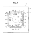
- FIG. 4 is a view similar to FIG. 2, and shows a simplification of the front surface of the semiconductor substrate 2 of the six-axis force sensor chip 1.
- the thin area in this embodiment is formed as thin area portions 31 through 34, as shown by the hatched area in FIG. 4, in positions corresponding to the four connecting parts 5A through 5D, respectively.
- the thin area portions 31 through 34 are formed as divided individual areas by subjecting the back surface of the semiconductor substrate 2 to dry etching or the like.
- Each of the four thin area portions 31 through 34 is formed so as to include the corresponding connecting parts 5A through 5D.
- the thin area portions 31 through 34 indicated by the hatched areas are formed as thin parts compared to the parts of other areas.
- the respective boundaries of the thin area portions 31 through 34 are not formed in the connecting parts 5A through 5D, but are formed in the supporting part 3 and operating part 4.
- the thin area portions 31 through 34 according to the present embodiment are set within a range in which there is a near match of the planar shapes that substantially include the connecting parts 5A through 5D. Accordingly, etching can be performed over a smaller surface area.
- the thin area portions 31 through 34 shown in FIG. 4 are separated from each other, but these areas may also be formed so that both respective end portions of the thin area portions 31 through 34 are connected to the end portions of the adjacent thin areas.
- FIG. 5 The front surface of the semiconductor substrate 2 of the six-axis force sensor chip 1 of this embodiment is shown in simplified form, and the location of the upper right corner part of the semiconductor substrate 2 shown in FIG. 4 is shown in a partial view.
- the thin area in the present embodiment are formed as thin area portions 41 and 42 corresponding to the connecting parts 5A and 5B, respectively, and indicated as hatched areas in FIG. 5.
- the thin area portions 41 and 42 are formed as divided individual areas by subjecting the back surface of the semiconductor substrate 2 to dry etching or the like.
- the left half of the thin area 41 is omitted in FIG. 5, and the lower half of the thin area 42 is also omitted.
- the thin area portions 41 and 42 both have a T shape.
- the thin area portions 41 and 42 are formed so as to include the corresponding connecting parts 5A and 5B and the holes A, B, L, M and K, and are formed with the same shape as the connecting parts (or a similar shape) but with a larger surface area than the connecting T-shaped parts.
- the thin area portions 41 and 42 indicated as the hatched areas are formed as thin parts compared to the parts of other areas.
- the thin area portions 41 and 42 of the connecting parts 5A and 5B are shown; however, thin areas of the other connecting parts 5C and 5D are also similarly formed.
- the respective boundaries of the thin area portions 31 through 34 are not formed in the connecting parts 5A through 5D, but are formed in the supporting part 3 and operating part 4.
- the thin areas in the present embodiment include the connecting parts 5A through 5D, and are formed so that these thin areas are considerably larger than the connecting parts.
- FIG. 6 is a perspective view of the external appearance of the force sensor
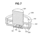
- FIG. 7 is a sectional perspective view illustrating the internal structure of the force sensor.
- the essential parts of a force sensor 300 are constructed from a force sensor chip 101 and a shock-absorbing device 102.
- the force sensor chip 101 is one of the force sensor chips 1 described in the embodiments.
- the force sensor 300 is constructed from a cylindrical rod-form input part 301 to which an external force (axial force or load) F1 is directly applied, a sensor mount 302 that has a relatively flat cylindrical shape (or ring shape) with a short length in the axial direction and is used to mount the force sensor 300 in a specified location, a discoid chip seat 303 that is used to attach the force sensor chip 101, a circular plate 304 having a damping or shock-absorbing function, and a transmission part 104 for connecting the input part 301 and the operating part 103 of the force sensor chip 101.
- the circular plate 304 forms the damping mechanism part of the shock-absorbing device 102 described above.
- the circular plate 304 and the discoid chip seat 303 are disposed parallel to each other in relatively close positions.
- the circular plate 304 and chip seat 303 both have holes formed in the central part.
- the back surface of the force sensor chip 101 is mounted via a glass part (not shown) to a part of the hole formed in the central part of the discoid chip seat 303.
- the rod-form transmission part 104 is disposed so that this part passes through the hole in the chip seat 303 and connects the undersurface of the input part 301 and the operating part 103 of the force sensor chip 101.
- the chip seat 303 and transmission part 104 are adjacent to each other on the same side of the force sensor chip 101. Furthermore, using a layout such as that of the damping device 102 shown in FIGS. 6 and 7 allows the entire construction of the damping device 102 to be located on the same side of the force sensor chip 101 (on the upper side of the force sensor chip 101 in FIG. 7), and the force sensor chip 101 can be joined by post-assembly after two or more of the parts comprising the input part 301, circular plate 304, sensor mount 302, transmission part 104 and chip seat 303 are integrally formed.
- the transmission part 104, damping mechanism part 304, and chip seat 303 are disposed on the side of the same surface of the force sensor chip 101; the damping mechanism part 304 is disposed on the inner circumferential side of the sensor mount 302; and the transmission part 104 is disposed on the inner circumferential side of the chip seat 303.
- a force sensor chip (1) having a multiaxial force sensing function is disclosed.
- the force sensor chip comprises a base member (2) having an operating part (4) provided with an external force application area (4A), a supporting part (3) for supporting the operating part, connecting parts (5A through 5D) for connecting the operating part and the supporting part, and strain resistance elements (Sxa1 through Sxa3, Sxb1 through Sxb3, Sya1 through Sya3, and Syb1 through Syb3) disposed in the connecting parts or within boundaries between the connecting parts and the operating part.
- the base member has a thin area (20) formed with a small thickness, and the boundaries of the thin area are disposed in the supporting part and operating part.
Abstract
Description
- The present invention relates to a force sensor chip and, more particularly, to a force sensor chip which has a plurality of strain resistance elements formed on the surface of a semiconductor substrate by using semiconductor manufacturing technology, and which is suitable for a six-axis force sensor or other device used as a compact force sensor in an industrial robot or the like.
- In automated industrial machines such as machine tools, industrial robots, and the like, forces are applied to workpieces, and the forces act from the outside because of the manner in which these machines operate. In this case, the forces and moments applied to the machines from the outside must be detected, and a control program that corresponds to these forces and moments must be performed. To ensure that a control program that corresponds to these forces and moments is carried out with a high degree of precision, the externally applied forces and moments must be accurately detected.
- In view of this situation, various types of force sensors have been proposed in the past. When classified based on the detection scheme, force sensors are usually divided into elastic force sensors and equilibrium force sensors. Elastic force sensors measure a force on the basis of the amount of deformation proportional to the external force. Equilibrium force sensors measure a force by balancing this force with a known force.
- Also known are force sensors whose structure is based on the principle that a plurality of strain resistance elements is installed in parts of a strain-generating body which undergoes elastic deformation in accordance with an external force. When an external force is applied to the strain-generating body of the force sensor, electrical signals corresponding to the degree of deformation of the strain-generating body are output from the plurality of strain resistance elements. Forces that have two or more components and are applied to the strain-generating body can be detected on the basis of these electrical signals. The measurement of the force generated by the force sensor can be calculated on the basis of these electrical signals.
- Six-axis force sensors constitute a known class of force sensors. Such six-axis force sensors are a class of elastic force sensors that comprise a plurality of strain resistance elements in parts of a strain-generating body. Six-axis sensors divide an external force into force components (forces: Fx, Fy, Fz) in the respective axial directions of three axes (X axis, Y axis, Z axis) of an orthogonal coordinate system, and into moment components (moments: Mx, My, Mz) about the respective axes, and detect the force as six-axis components.
- The present inventors previously proposed a six-axis force sensor having a novel construction (see
JP 2003-207405 A1 -
JP 2001-264198 A1 JP 2001-264198 A1 - In the six-axis force sensor described in
JP 2003-207405 A1 - On the other hand, in the multiaxial force sensor described in
JP 2001-264198 A1 - It is an object of the present invention to provide, in light of the above problems, a force sensor chip in which a favorable detection balance can be maintained between the respective axial forces even when the planar shape is made compact, in which the concentration of stress in the connecting parts by applied external forces can be prevented to avoid chip damage, and in which the connecting parts can be sufficiently flexed so that the detection sensitivity can be increased while making it less likely that design errors will occur in the amounts of strain detected by the respective strain detection elements.
- According to an aspect of the present invention, there is provided a force sensor chip having a multiaxial force sensing function, the force sensor chip comprising: a base member having an operating part provided with an external force application area; a supporting part for supporting the operating part; connecting parts for connecting the operating part and the supporting part; and strain resistance elements disposed in the connecting parts or within boundaries between the connecting parts and the operating part, wherein the base member has a thin area formed with a small thickness, and the boundaries of the thin area are disposed in the supporting part and the operating part.
- The thin area formed in the base member is formed to include the areas of the connecting parts. As a result, when the planar shape of the chip as such is made compact, the overall degree of deformation of the connecting parts is increased by the presence of the thin area, and the detection balance between the respective axial forces can be maintained as the chip is made more compact.
- Preferably, the thin area has boundaries disposed in an area of a predetermined range extending from outside end portions of the connecting parts to an end portion of the base member, and in an area of a predetermined range extending from an end portion of the external force application area to inside end portions of the connecting parts.
- Desirably, the thin area is formed to include as a whole each of the connecting parts.
- Preferably, the thin area includes as a whole each of the connecting parts, and is formed corresponding to the connecting parts.
- In a preferred form, the base member is bored to have openings that functionally separate the base member into the supporting part, the operating part and the connecting parts.
- It is preferable that the openings be long slots.
- It is desirable that each of the connecting parts have a bridge part provided with an area of high rigidity, and an elastic part provided with an area of low rigidity.
- Preferably, the thin area has boundaries that are disposed inside an area of a predetermined range extending from an end portion of the base member to end portions of the elastic parts, and inside an area of a predetermined range extending from an end portion of the external force application area to end portions of the bridge parts.
- Desirably, the thin area is an annular area that surrounds the external force application area of the operating part.
- Preferably, the thin area is formed on a back surface of the base member.
- Desirably, the base member is a semiconductor substrate, and the thin area is formed by a dry etching treatment.
- The thin area formed in the base member is formed to include the areas in which the connecting parts are formed, and the degree of deformation of the connecting parts can therefore be increased. Accordingly, even if the chip is made compact in the planar direction, a favorable detection balance can be maintained between the respective axial forces as the chip is made more compact. In particular, since the boundary between the thin part of the thin area and the thick parts of other areas is formed in the supporting part and the operating part, a favorable detection balance can be maintained between the respective axial forces without affecting the connecting parts.
- If the boundary of the thin area is formed in the supporting part and operating part as described above, a state of concentrated stress in the connecting parts can be avoided, and damage to the base member, i.e., to the chip, can be prevented.
- Since the degree of deformation of the connecting parts overall can be increased by forming the thin area, strain can be effectively generated in the parts where deformation of the connecting parts is generated, and the detection sensitivity can be increased.
- Certain preferred embodiments of the present invention will be described in detail below, by way of example only, with reference to the accompanying drawings, in which:
- FIG. 1 is a plan view showing a force sensor chip according to a first embodiment of the present invention;
- FIG. 2 is a top plan view showing in simplified manner the front surface of the semiconductor substrate of the force sensor chip according to the first embodiment of the present invention;
- FIG. 3A is a schematic view showing the upper surface of the force sensor chip in further simplified manner and in cross section along line A-A;
- FIG. 3B is a schematic view showing the back surface of the force sensor chip in further simplified manner and in cross section along line B-B;
- FIG. 4 is a view similar to FIG. 2, showing a force sensor chip according to a second embodiment of the present invention;
- FIG. 5 is a top plan view showing essential parts of a modification of the force sensor chip according to the second embodiment;
- FIG. 6 is a perspective view showing an example of assembly of the force sensor chip with the sensor unit; and
- FIG. 7 is a longitudinal sectional view of the force sensor shown in FIG. 6.
- A first embodiment of the force sensor chip of the present invention will be described with reference to FIGS. 1 through 3. In this embodiment, an example of a six-axis force sensor chip is described as a force sensor chip. The force sensor chip of the present invention is not limited to a six-axis force sensor chip.
- FIG. 1 is a plan view showing the front surface of the force sensor chip. In the force sensor chip of FIG. 1, all of the strain resistance elements and temperature compensation resistance elements show a pattern comprising a plurality of holes and electrode pads.
- In FIG. 1, the six-axis
force sensor chip 1 of the present embodiment is formed using a semiconductor substrate which preferably has a square planar shape. For example, the length of one side of this square semiconductor substrate is 5.5 mm. The substrate is not limited to a semiconductor substrate. The six-axisforce sensor chip 1 has a plate-form shape based on the semiconductor substrate. - In the six-axis
force sensor chip 1, in cases where a semiconductor device is formed on the substrate, the square semiconductor substrate is provided with a planar shape, specified holes are formed, and the substrate itself is processed by applying semiconductor manufacturing process technology (treatments such as patterning, etching, ion implantation, P-CVD, sputtering, RIE, and the like) to one surface (front surface), and the chip is manufactured by forming a film in a specified area of the front surface of the semiconductor substrate. - Thus, the six-
axis sensor chip 1 of the present embodiment is formed as a semiconductor sensor device. - In the six-
axis sensor chip 1, the functional part for detecting six-axis components as a six-axis force sensor is formed by 12 strain resistance elements (or piezo-resistance elements, hereafter referred to as "resistance elements," meaning strain resistance elements) Sxa1 through Sxa3, Sxb1 through Sxb3, Sya1 through Sya3, and Syb1 through Syb3 composed of active layers (or thermal diffusion layers) formed by ion implantation in the front surface of asemiconductor substrate 2. The total of 12 strain resistance elements are disposed as sets of three elements each (Sxa1, Sxa2, Sxa3), (Sxbl, Sxb2, Sxb3), (Sya1, Sya2, Sya3), and (Syb1, Syb2, Syb3) along the area adjacent to the edge of the boundary with the operatingpart 4 in four connectingparts 5A through 5D having a below-described inverted T shape (or T shape). - Furthermore, temperature
compensation resistance elements 11 composed of active layers (thermal diffusion layers) are separately formed in the six-axisforce sensor chip 1 in positions corresponding to the 12 resistance elements Sxa1 through Sxa3, Sxb1 through Sxb3, Sya1 through Sya3, and Syb1 through Syb3. - As is shown in FIG. 1, the
semiconductor substrate 2 has holes A, B, C, D, K, L, M, and N formed by boring so that these holes pass through in the direction of thickness of the plate member. The six-axisforce sensor chip 1 is functionally separated into the supporting part, the operating part, and the connecting parts by the holes A, B, C, D, K, L, M, and N. - The holes A, B, C, D, K, L, M, and N all have a slit-form shape that has a relatively narrow width. The holes A, B, C, and D have a substantially rectilinear slit shape, and the holes K, L, M, and N have a slit shape resembling the letter L.
- The
semiconductor substrate 2 that forms the six-axisforce sensor chip 1 is constructed from an operatingpart 4 which has a planar shape resembling a square shape positioned in the center, a supportingpart 3 which has a substantially square ring shape in a position surrounding this operatingpart 4, and four connectingparts part 4 and supportingpart 3, and which connect both of these parts in positions corresponding to the respective parts of the four sides. The operatingpart 4 is formed by the holes K, L, M, and N. The four T-shaped connectingparts - Furthermore, in cases where the strain resistance elements are disposed on the connecting parts, the arrangement is not necessarily limited to locations where maximum stress is generated in the connecting parts. The strain resistance elements are disposed by taking into account various other conditions, such as the formation process, wiring route, and the like.
- In the
semiconductor substrate 2 having the above configuration, for example, when the surrounding supportingpart 3 is assembled with the six-axis force sensor unit, this supportingpart 3 is joined to a support seat (e.g., thechip seat 303 shown in FIG. 7 described later). - Silicon and glass, or glass and a metal can usually be joined by anodic joining, but direct anodic joining between silicon and a metal is not possible. Accordingly, the support seat and a metal part that transmits external forces, such as a connecting rod or the like, are jointed via a glass part. This point will be explained in detail later.
- Furthermore, for example, when the operating
part 4 is assembled with the six-axis force sensor unit, and external forces, loads, or the like (hereafter referred to as "external loads") are transmitted via a connecting rod or the like (e.g., the transmittingpart 104 shown in FIG. 7 described later), the operatingpart 4 is the part that directly receives the action of these external forces. The operatingpart 4 is ordinarily constructed so as to receive external forces in the central portion thereof. Furthermore, when the operatingpart 4 receives an external force and undergoes a change in position, the connectingparts - The operating
part 4 is formed from a central part (external force application area) 4A to which external forces are applied or input, and is also formed from fourcorner parts 4B corresponding to the four corners positioned around thecentral part 4A. Thecircle 4C indicated by a broken line is a connection area where a connecting rod that transmits external forces and the like is connected. For example, the diameter of thecircle 4C is 1.6 mm. The outer edge parts of the fourcorner parts 4B in theoperating part 4 are formed as free ends by the holes K, L, M, and N. Accordingly, the areas adjacent to the free ends of the fourcorner parts 4B are non-deformation areas in which no deformation occurs in the parts themselves even in cases where an external force is applied to thecentral part 4A. - In the
operating part 4, thecentral part 4A is a part where external forces are applied or input. As is shown in FIG. 2, the four surrounding connectingparts 5A through 5D are substantially T-shaped bridges and have a bridge part 5Aa and elastic part 5Ab, a bridge part 5Ba and elastic part 5Bb, a bridge part 5Ca and elastic part 5Cb, and a bridge part 5Da and elastic part 5Db, respectively. The elastic parts 5Ab, 5Bb, 5Cb, and 5Db of the connectingparts 5A through 5D are connected to the supportingpart 3 at both end portions in the longitudinal direction in the areas on the inside of the holes A, B, C, and D, respectively. In each of the bridge parts 5Aa, 5Ba, 5Ca, and 5Da of the connectingparts 5A through 5D, one end portion in the longitudinal direction (the inside end portion) is connected to a part corresponding to one side of the operatingpart 4, and the other end portion (outside end portion) is connected to the corresponding elastic part. - In order to disperse the stress caused by external forces applied to the
operating part 4 and to provide strength against applied external forces, the peripheries of the boundaries between the operatingpart 4 and the bridge parts 5Aa, 5Ba, 5Ca, and 5Da and elastic parts 5Ab, 5Bb, 5Cb, and 5Db are worked, preferably rounded, into a circular arc shape and connected. The shapes of the holes A through D and K through N are not limited to the shapes shown in the present embodiment. The holes A through D and K through N are formed by taking into account the size of the six-axisforce sensor chip 1, the number of strain resistance elements, the detectable stress range, and the like so that strain is most conspicuously generated in the parts of the 12 strain resistance elements Sxa1 through Sxa3, Sxb1 through Sxb3, Sya1 through Sya3, and Syb1 through Syb3 and not generated in the positions of the temperaturecompensation resistance elements 11, and so that the temperature conditions are the same in the 12 strain resistance elements. For example, the linear lengths of the end portions of the holes K through N (the parts of the holes extending from the bridge parts 5Aa through 5Da to the respective temperature compensation elements) may be made longer than the lengths shown in FIGS. 1 and 2. - In the structural example shown in FIG. 1, the connecting
parts 5A through 5D are formed substantially with a T shape (as T beams) by the holes A, B, C, D, K, L, M, and N formed as through-holes in thesemiconductor substrate 2. However, as long as these parts provide the required elastic function, the parts may be formed with some other shape, such as a Y shape or the like. - In FIG. 1, for example, the resistance elements Sya1, Sya2, Sya3, and the like are formed adjacent to the boundary between the operating
part 4 and the bridge part 5Aa in the connectingpart 5A. Specifically, on the front surface of the connectingpart 5A, stress is generated in accordance with external forces applied to theoperating part 4. Accordingly, these elements are formed so that the elements are disposed in parts where strain is most conspicuously generated. Furthermore, the resistance elements Sya1, Sya2, and Sya3 are lined up in the direction of width of the bridge part 5Aa, and are formed so that these elements are spaced at equal intervals, with the longitudinal directions of the elements parallel to the direction of the longitudinal axis of the bridge part 5Aa. The central resistance elements Sya2, Sxa2, Syb2, and Sxb2 are disposed on the center line in the longitudinal direction of the respective bridge parts. - Similar to the resistance elements Sya1 through Sya3 described above, the other resistance elements Syb1 through Syb3, resistance elements Sxa1 through Sxa3, and
resistance elements Sxb 1 through Sxb3 are formed so that these resistance elements are disposed adjacent to the boundary between the operatingpart 4 and bridge part 5Ca, adjacent to the boundary between the operatingpart 4 and bridge part 5Ba, and adjacent to the boundary between the operatingpart 4 and bridge part 5Da. - Substantially square annular GND (ground)
wiring 13 is disposed across the required width along the respective sides around the periphery of thesemiconductor substrate 2. Twoelectrode pads 14 are connected to theGND wiring 13. - A total of 26
signal electrode pads 16 are formed along each of a pair of opposite sides in thesemiconductor substrate 2. Thirteensignal electrode pads 16 are lined up along each of these sides. Two remainingelectrode pads 17 are additional electrode pads. Theseadditional electrode pads 17 are provided in order to make the potential in the plane of the semiconductor substrate uniform by being connected to an external GND potential or bias potential. The number ofadditional electrode pads 17 is not limited to two, and three or more of these electrode pads may be installed. The squareannular GND wiring 13 shown in FIG. 1 is merely an example; this function can be fulfilled as long as a constant potential is afforded. - In the six-axis
force sensor chip 1, the 12 temperaturecompensation resistance elements 11 which are separately installed corresponding to each of the 12 resistance elements Sxa1 through Sxa3, Sxb1 through Sxb3, Sya1 through Sya3, and Syb1 through Syb3 are disposed on the peripheral edge parts of the fourcorner parts 4B, which are non-deformation areas. The resistance elements and temperaturecompensation resistance elements 11 are related in a one-to-one correspondence. The 12 temperaturecompensation resistance elements 11 are formed on the surface of the peripheral edge parts of thecorner parts 4B, which have substantially the same temperature conditions as the corresponding resistance elements and do not deform even when the operatingpart 4 receives an external force. The results of measuring variations in the resistance of the resistance elements used for external force measurement are constantly corrected on the basis of variations in the resistance of the temperaturecompensation resistance elements 11 that are unaffected by external forces, so that the measurement of forces and moments unaffected by the ambient temperature is possible. - Here, one example of the method used to manufacture the six-axis
force sensor chip 1 will be described. For example, boron, which is a p-type impurity, is implanted as ions into a semiconductor substrate made of n-type (100) silicon using a resistance element formation pattern formed by photolithography, and thesemiconductor substrate 2 is heated so that an activation treatment of the implanted boron is performed, thus forming active layers. The resistance elements that are formed on the front surface of thesemiconductor substrate 2 are the temperaturecompensation resistance elements 11 and the strain resistance elements Sya1 through Sya3, Syb1 through Syb3, Sxa1 through Sxa3 and Sxb1 through Sxb3. Subsequently, a silicon oxide film is formed as an inter-layer insulating film by p-CVD (plasma chemical vapor growth method). - Subsequently, a resist pattern used to form contact holes is formed, and the inter-layer insulating film in the areas where the contact holes are to be formed is removed by means of BHF (buffered hydrofluoric acid) using this resist pattern as a mask. Then, the resist pattern is removed, Al or Al-Si (an alloy of aluminum and silicon) is sputtered over the entire front surface of the
semiconductor substrate 2, and a heat treatment used to form an ohmic junction is performed. This results in the formation of contacts for the active layers and contacts between the various types of electrodes and thesemiconductor substrate 2. - Subsequently, a resist pattern used to form GND wiring, signal wiring, and the like is formed together with the respective electrode areas by photolithography, and patterning of the respective wiring and electrodes is performed by removing the unnecessary metal parts by wet etching. The resist pattern is then removed, and an SiN film (silicon nitride film) is formed as a passivation film by p-CVD. Subsequently, holes A, B, C, D, K, L, M, and N are formed in the
semiconductor substrate 2 by RIE (reactive ion etching), and sensor chip are divided (sensor chips 1 are cut out from the wafer) by dicing. Instead of being divided by dicing, sensor chips can sometimes be cut by an etching treatment using RIE. - Next, the thin area of the six-axis
force sensor chip 1 provided with the above-described structure on the front surface will be described with reference to FIGS. 2, 3A, and 3B. - FIG. 2 shows the front surface of the
semiconductor substrate 2 of the six-axisforce sensor chip 1 in simplified form, FIG. 3A shows a plan view (A) and a cross section along line A-A (B) of the further simplified chip front surface, and FIG. 3B shows an underside view (A) and a cross section along line B-B (B) of the chip back surface. The relationship of the joining alignment of the glass parts joined to the back surface of the chip (described later) is also shown in the sectional view (B) of FIG. 3A and the sectional view (B) of FIG. 3B. - As is shown in FIG. 2, the
thin area 20 is the area indicated by shading between theoutside boundary 21 and insideboundary 22. As is shown in FIG. 3A (B) and FIG. 3B (B), thethin area 20 is formed as a thin part by subjecting the back surface of thesemiconductor substrate 2 to dry etching or the like. The etching of thesemiconductor substrate 2 is set as a step of the method used to manufacture the six-axisforce sensor chip 1. - The thickness can also be reduced by wet etching, but the thin area can be formed with greater precision by using a dry etching treatment such as RIE or the like, which is superior in terms of finer processing precision.
- The
thin area 20 in the plan view of the chip shown in (A) of FIG. 3A and in the undersurface view of the chip shown in (B) of FIG. 3B can be clearly shown based on the correspondence relationship with the thin part shown in the sectional views of the respective figures. - As is shown in (B) of FIG. 3A, (B) of FIG. 3B, and the like,
glass parts semiconductor substrate 2 that remain as a result of the formation of thethin area 20 on the back surface of thesemiconductor substrate 2, i.e., the thick parts of the supportingpart 3 and operatingpart 4. Theglass part 25 is joined to the supportingpart 3, and theglass part 26 is joined to theoperating part 4. From the standpoint of the joining alignment described above, a design is selected so that the surface along which the supportingpart 3 is joined to theglass part 25 is narrower than the surface of theglass part 25 that faces the supportingpart 3. Similarly, the surface along which theoperating part 4 is joined to theglass part 26 is designed wider than the surface of theglass part 26 that faces the operatingpart 4. In other words, from the standpoint of the joining alignment with the glass parts, the shape and area of thethin area 20 of thesemiconductor substrate 2 are specifically selected. - Silicon and glass, and glass and metal can usually be joined by anodic joining, but direct anodic joining between silicon and metal is not possible. Accordingly, in the present embodiment, as is shown in FIGS. 3A and 3B, anodic joining is made possible via the
respective glass parts part 3, and in the joint between the operatingpart 4 and the connecting rod (metal, not shown) that transmits external forces to theoperating part 4. - Furthermore, in the anodic joining treatment, it is necessary to align the
glass parts part 3 and operatingpart 4 of the six-axisforce sensor chip 1. - In the present embodiment, the thin area is made larger than in existing conventional techniques. Accordingly, the plane surface area of the thick parts of the supporting
part 3 and operatingpart 4 can be made smaller than the plane surface area of theglass parts sensor chip 1 is somewhat shifted during alignment, the joining surfaces of the supportingpart 3 and operatingpart 4 originally scheduled for joining can be stipulated from the sensor chip. From the standpoint of this joining alignment, the joining surface on the back surface of the chip (the remaining parts that are not made thinner) is preferably made smaller than the joining surface of the joined glass parts. In other words, it may be said that a configuration in which the thin area is larger is preferred to provide better joining surfaces with the glass parts. - The
thin area 20 in the first embodiment has an annular shape. The annular planar shape has the advantage of being able to simplify the adjustment of the alignment with theglass parts outside boundary 21 of the annularthin area 20 is formed on the back surface of the part where the supportingpart 3 is formed. Theinside boundary 22 of thethin area 20 is the part that forms the operatingpart 4, and the boundary is formed on the back surface of the area surrounding the central part (external force application area) 4A to which external forces are applied. As a result, thethin area 20 is formed as an area that includes all of the connectingparts 5A through 5D. - Next, the position of the
outside boundary part 21 and the position of theinside boundary part 22 that determine the range of thethin area 20 will be described. Here, the "distance W0" and the "distance W3" are defined as shown in FIG. 2. For example, the "distance W0" is the distance from the outside end portion (end portion of the elastic part) 27 of the connectingpart 5A to the edge of thesemiconductor substrate 2. Furthermore, for example, the "distance W3" is the distance from the inside end portion (end portion of the bridge part) 28 of the connectingpart 5A to the externalforce application area 4A of the operatingpart 4. - In the
thin area 20, the position of theoutside boundary 21 formed on the supportingpart 3 is between the outside end portions (boundary between the connecting part and supporting part) 27 of the respective connecting parts and the edge of thesemiconductor substrate 2. In other words, forming thethin area 20 on the back surface of thesemiconductor substrate 2 allows the position of theoutside boundary 21 to be set in a range in which there is no loss of functionality for the supporting part 3 (i.e., in which the joining area with the external structural body is retained and no problems are created in terms of strength). The range for setting the outside boundary of the thin area can be expressed as the distance W1 shown in FIG. 2. In this case, the distance W1 may be set, for example, so that thecondition 0 < W1 < W0 ≤ 0.9 is satisfied. Here, 0 < W1 means that the position of theoutside boundary 21 faces the edge of thesemiconductor substrate 2, beginning with theoutside end portion 27 of the connecting part as the starting point. - The position (fig. 15) of the
inside boundary 22 formed in theoperating part 4 is between the edge of the externalforce application area 4A and the inside end portion (boundary between the connecting part and operating part) 28 of the connecting part. In other words, by forming thethin area 20 on the back surface of thesemiconductor substrate 2, the position of theinside boundary 22 is set in a range in which there is no loss of functionality for the operating part 4 (i.e., in which the joining area with the member that transmits external forces, such as a connecting rod or the like, is retained, and no problems are created in terms of strength). The range for setting the inside boundary of the thin area can be expressed as the distance W2 shown in FIG. 2. In this case, the distance W2 may be set (for example) so that thecondition 0 ≤ W2 < W3 is satisfied. Here, 0 ≤ W2 means that the position of theinside boundary 22 faces the edge of theinside end portion 28 of the connecting part, beginning with the external force application area as the starting point. - In this case, the outside boundary and inside boundary of the thin area are set so that these boundaries do not fall on the connecting parts. As a result of the positions of the boundaries of the thin area thus being set, an unnecessary concentration of stress in the boundaries between the thick parts and thin parts of the connecting parts can be avoided.
- Furthermore, in the
thin area 20, thenon-deformation areas 4B, which are the four corner parts of the operatingpart 4, are not parts that have an effect on the measurement of axial forces in the thin area formed on the back surface of the operatingpart 4. Accordingly, a reduction in thickness is not always necessary, but such a reduction is still desirable to improve the alignment with theglass parts - Next, a second embodiment of the thin area formed in the six-axis
force sensor chip 1 will be described with reference to FIG. 4. FIG. 4 is a view similar to FIG. 2, and shows a simplification of the front surface of thesemiconductor substrate 2 of the six-axisforce sensor chip 1. - The thin area in this embodiment is formed as
thin area portions 31 through 34, as shown by the hatched area in FIG. 4, in positions corresponding to the four connectingparts 5A through 5D, respectively. As in the case of the first embodiment, thethin area portions 31 through 34 are formed as divided individual areas by subjecting the back surface of thesemiconductor substrate 2 to dry etching or the like. - Each of the four
thin area portions 31 through 34 is formed so as to include the corresponding connectingparts 5A through 5D. Thethin area portions 31 through 34 indicated by the hatched areas are formed as thin parts compared to the parts of other areas. In this embodiment as well, the respective boundaries of thethin area portions 31 through 34 are not formed in the connectingparts 5A through 5D, but are formed in the supportingpart 3 and operatingpart 4. - The
thin area portions 31 through 34 according to the present embodiment are set within a range in which there is a near match of the planar shapes that substantially include the connectingparts 5A through 5D. Accordingly, etching can be performed over a smaller surface area. - The
thin area portions 31 through 34 shown in FIG. 4 are separated from each other, but these areas may also be formed so that both respective end portions of thethin area portions 31 through 34 are connected to the end portions of the adjacent thin areas. - Next, a modification of the second embodiment will be described with reference to FIG. 5. The front surface of the
semiconductor substrate 2 of the six-axisforce sensor chip 1 of this embodiment is shown in simplified form, and the location of the upper right corner part of thesemiconductor substrate 2 shown in FIG. 4 is shown in a partial view. - The thin area in the present embodiment, for example, are formed as
thin area portions parts thin area portions semiconductor substrate 2 to dry etching or the like. - The left half of the
thin area 41 is omitted in FIG. 5, and the lower half of thethin area 42 is also omitted. Thethin area portions thin area portions parts thin area portions thin area portions parts parts thin area portions 31 through 34 are not formed in the connectingparts 5A through 5D, but are formed in the supportingpart 3 and operatingpart 4. - The thin areas in the present embodiment include the connecting
parts 5A through 5D, and are formed so that these thin areas are considerably larger than the connecting parts. By reducing the thickness in such a shape, the surface area where thickness-reducing etching is performed can be reduced, and the design of the thin areas can be simplified. - Next, an example in which the force sensor of the six-axis
force sensor chip 1 formed by thesemiconductor substrate 2 having the shape described above is assembled with the sensor unit will be described with reference to FIGS. 6 and 7. - FIG. 6 is a perspective view of the external appearance of the force sensor, and FIG. 7 is a sectional perspective view illustrating the internal structure of the force sensor.
- The essential parts of a
force sensor 300 are constructed from aforce sensor chip 101 and a shock-absorbingdevice 102. Theforce sensor chip 101 is one of theforce sensor chips 1 described in the embodiments. Theforce sensor 300 is constructed from a cylindrical rod-form input part 301 to which an external force (axial force or load) F1 is directly applied, asensor mount 302 that has a relatively flat cylindrical shape (or ring shape) with a short length in the axial direction and is used to mount theforce sensor 300 in a specified location, adiscoid chip seat 303 that is used to attach theforce sensor chip 101, acircular plate 304 having a damping or shock-absorbing function, and atransmission part 104 for connecting theinput part 301 and theoperating part 103 of theforce sensor chip 101. Thecircular plate 304 forms the damping mechanism part of the shock-absorbingdevice 102 described above. - The
circular plate 304 and thediscoid chip seat 303 are disposed parallel to each other in relatively close positions. Thecircular plate 304 andchip seat 303 both have holes formed in the central part. Furthermore, in a position on the lower side (outside) of thechip seat 303, the back surface of theforce sensor chip 101 is mounted via a glass part (not shown) to a part of the hole formed in the central part of thediscoid chip seat 303. The rod-form transmission part 104 is disposed so that this part passes through the hole in thechip seat 303 and connects the undersurface of theinput part 301 and theoperating part 103 of theforce sensor chip 101. - In the
force sensor 300, thechip seat 303 andtransmission part 104 are adjacent to each other on the same side of theforce sensor chip 101. Furthermore, using a layout such as that of the dampingdevice 102 shown in FIGS. 6 and 7 allows the entire construction of the dampingdevice 102 to be located on the same side of the force sensor chip 101 (on the upper side of theforce sensor chip 101 in FIG. 7), and theforce sensor chip 101 can be joined by post-assembly after two or more of the parts comprising theinput part 301,circular plate 304,sensor mount 302,transmission part 104 andchip seat 303 are integrally formed. - To reduce the thickness of the
force sensor 300, thetransmission part 104, dampingmechanism part 304, andchip seat 303 are disposed on the side of the same surface of theforce sensor chip 101; the dampingmechanism part 304 is disposed on the inner circumferential side of thesensor mount 302; and thetransmission part 104 is disposed on the inner circumferential side of thechip seat 303. - When an external force F1 is applied to the
input part 301, thecircular plate 304 is deformed by the external force F1, and this external force F1 is dampened and transmitted to theoperating part 103 of theforce sensor chip 101. - A force sensor chip (1) having a multiaxial force sensing function is disclosed. The force sensor chip comprises a base member (2) having an operating part (4) provided with an external force application area (4A), a supporting part (3) for supporting the operating part, connecting parts (5A through 5D) for connecting the operating part and the supporting part, and strain resistance elements (Sxa1 through Sxa3, Sxb1 through Sxb3, Sya1 through Sya3, and Syb1 through Syb3) disposed in the connecting parts or within boundaries between the connecting parts and the operating part. The base member has a thin area (20) formed with a small thickness, and the boundaries of the thin area are disposed in the supporting part and operating part.
Claims (11)
- A force sensor chip (1) having a multiaxial force sensing function, comprising:a base member (2) having an operating part (4) provided with an external action area part (4A), a supporting part (3) for supporting the operating part, and connecting parts (5A through 5D) for connecting the operating part and the supporting part; andstrain resistance elements (Sxa1 through Sxa3, Sxb1 through Sxb3, Sya1 through Sya3, and Syb 1 through Syb3) disposed in the connecting parts or within boundaries between the connecting parts and the operating part,wherein the base member has a thin area (20) formed with a small thickness, and the boundaries of the thin area are disposed in the supporting part and the operating part.
- The force sensor chip of claim 1, wherein the thin area (20) has boundaries disposed in an area of a predetermined range extending from outside end portions of the connecting parts (5A through 5D) to an end portion of the base member (2), and in an area of a predetermined range extending from an end portion of the external force application area (4A) to inside end portions of the connecting parts.
- The force sensor chip of claim 1, wherein the thin area (20) is formed to include as a whole each of the connecting parts (5A through 5D).
- The force sensor chip of claim 1, wherein the thin area (20) includes as a whole each of the connecting parts (5A through 5D), and is formed corresponding to the connecting parts.
- The force sensor chip of claim 1, wherein the base member (2) is bored to have openings (A through D and K through N) that functionally separate the base member into the supporting part (3), the operating part (4) and the the connecting parts (5A through 5D).
- The force sensor chip of claim 5, wherein the openings (A through D and K through N) are long slots.
- The force sensor chip of claim 5, wherein each of the connecting parts (5A through 5D) has a bridge part (5Aa, 5Ba, 5Ca, 5Da) provided with an area of high rigidity, and an elastic part (5Ab, 5Bb, 5Cb, 5Db) provided with an area of low rigidity.
- The force sensor chip of claim 7, wherein the thin area (20) has boundaries that are disposed inside an area of a predetermined range extending from an end portion of the base member (2) to end portions of the elastic parts (5Ab, 5Bb, 5Cb, 5Db), and inside an area of a predetermined range extending from an end portion of the external force application area (4A) to end portions of the bridge parts (5Aa, 5Ba, 5Ca, 5Da).
- The force sensor chip of claim 1, wherein the thin area (20) is an annular area that surrounds the external force application area (4A) of the operating part (4).
- The force sensor chip of claim 1, wherein the thin area (20) is formed on a back surface of the base member (2).
- The force sensor chip of claim 1, wherein the base member (2) is a semiconductor substrate, and the thin area (20) is formed by a dry etching treatment.
Applications Claiming Priority (1)
| Application Number | Priority Date | Filing Date | Title |
|---|---|---|---|
| JP2006128384A JP5303101B2 (en) | 2006-05-02 | 2006-05-02 | Force sensor chip |
Publications (3)
| Publication Number | Publication Date |
|---|---|
| EP1852688A2 true EP1852688A2 (en) | 2007-11-07 |
| EP1852688A3 EP1852688A3 (en) | 2008-03-12 |
| EP1852688B1 EP1852688B1 (en) | 2010-10-20 |
Family
ID=38330496
Family Applications (1)
| Application Number | Title | Priority Date | Filing Date |
|---|---|---|---|
| EP07008878A Not-in-force EP1852688B1 (en) | 2006-05-02 | 2007-05-02 | Multiaxial force sensor chip |
Country Status (5)
| Country | Link |
|---|---|
| US (1) | US7536923B2 (en) |
| EP (1) | EP1852688B1 (en) |
| JP (1) | JP5303101B2 (en) |
| AT (1) | ATE485498T1 (en) |
| DE (1) | DE602007009893D1 (en) |
Cited By (2)
| Publication number | Priority date | Publication date | Assignee | Title |
|---|---|---|---|---|
| CN110325832A (en) * | 2017-02-24 | 2019-10-11 | 日本电产科宝电子株式会社 | Response body and the force snesor for having the response body |
| EP3495794A4 (en) * | 2016-10-07 | 2020-04-01 | Minebea Mitsumi Inc. | Sensor chip, strain inducing body, and force sensor device |
Families Citing this family (15)
| Publication number | Priority date | Publication date | Assignee | Title |
|---|---|---|---|---|
| JP5243704B2 (en) * | 2006-08-24 | 2013-07-24 | 本田技研工業株式会社 | Force sensor |
| JP4909104B2 (en) * | 2007-01-31 | 2012-04-04 | 本田技研工業株式会社 | Force sensor |
| US8476005B2 (en) * | 2008-02-05 | 2013-07-02 | California Institute Of Technology | Microfluidic embedded polymer NEMS force sensors |
| DE102008061769A1 (en) * | 2008-12-11 | 2010-06-17 | Bayerische Motoren Werke Aktiengesellschaft | Internal combustion engine and compression ignition combustion method |
| JP5024358B2 (en) * | 2009-01-08 | 2012-09-12 | 株式会社日本自動車部品総合研究所 | Action force detector |
| JP5243988B2 (en) * | 2009-02-10 | 2013-07-24 | 本田技研工業株式会社 | Multi-axis force sensor and acceleration sensor |
| US8857275B2 (en) | 2011-05-02 | 2014-10-14 | California Institute Of Technology | NEMS sensors for cell force application and measurement |
| DE102011112935B4 (en) * | 2011-09-13 | 2015-02-12 | Micronas Gmbh | force sensor |
| CN102944339A (en) * | 2012-10-22 | 2013-02-27 | 北京大学 | Piezoresistive pressure sensor of MEMS (Micro-Electro-Mechanical Systems) and preparation method thereof |
| WO2018066557A1 (en) * | 2016-10-07 | 2018-04-12 | ミツミ電機株式会社 | Sensor chip, strain inducing body, and force sensor device |
| JP6940037B2 (en) * | 2017-04-26 | 2021-09-22 | ミネベアミツミ株式会社 | Force sensor device |
| US10634695B2 (en) * | 2017-04-26 | 2020-04-28 | Minebea Mitsumi Inc. | Force sensor |
| JP2022101139A (en) * | 2020-12-24 | 2022-07-06 | ミネベアミツミ株式会社 | Sensor chip and inner force sensor device |
| JP2022142116A (en) * | 2021-03-16 | 2022-09-30 | ミネベアミツミ株式会社 | Strain body and force sensor device |
| JP2022142117A (en) * | 2021-03-16 | 2022-09-30 | ミネベアミツミ株式会社 | Sensor chip, and force sensor device |
Family Cites Families (17)
| Publication number | Priority date | Publication date | Assignee | Title |
|---|---|---|---|---|
| JPS57169643A (en) * | 1981-04-13 | 1982-10-19 | Yamato Scale Co Ltd | Load cell for multiple components of force |
| JPH0821721B2 (en) * | 1986-10-09 | 1996-03-04 | 株式会社リコー | Force detection device |
| US5263375A (en) * | 1987-09-18 | 1993-11-23 | Wacoh Corporation | Contact detector using resistance elements and its application |
| US6864677B1 (en) * | 1993-12-15 | 2005-03-08 | Kazuhiro Okada | Method of testing a sensor |
| JP3171970B2 (en) * | 1992-12-10 | 2001-06-04 | 株式会社ワコー | Force / acceleration detector |
| KR100199691B1 (en) * | 1997-05-19 | 1999-06-15 | 김동진 | 6-component load cell |
| JPH11333765A (en) * | 1998-05-26 | 1999-12-07 | Tokai Rika Co Ltd | Micro-manipulator having force sensor |
| JP2001264198A (en) | 2000-03-16 | 2001-09-26 | Olympus Optical Co Ltd | Method for manufacturing multiaxial tactile sensor and tactile sensor |
| EP1327870B1 (en) | 2002-01-11 | 2013-05-08 | Honda Giken Kogyo Kabushiki Kaisha | Six-axis force sensor |
| JP4011345B2 (en) * | 2002-01-11 | 2007-11-21 | 本田技研工業株式会社 | Multi-axis force sensor chip |
| JP2005049320A (en) * | 2003-07-30 | 2005-02-24 | Microstone Corp | Acceleration sensor |
| JP4680566B2 (en) * | 2004-10-26 | 2011-05-11 | 本田技研工業株式会社 | Multi-axis force sensor chip and multi-axis force sensor using the same |
| JP4203051B2 (en) * | 2005-06-28 | 2008-12-24 | 本田技研工業株式会社 | Force sensor |
| JP5007083B2 (en) * | 2006-08-08 | 2012-08-22 | 本田技研工業株式会社 | Force sensor chip |
| JP4210296B2 (en) * | 2006-08-24 | 2009-01-14 | 本田技研工業株式会社 | Method for manufacturing force sensor |
| JP4958501B2 (en) * | 2006-08-30 | 2012-06-20 | 本田技研工業株式会社 | Force sensor chip and external force transmission mechanism |
| JP2008058110A (en) * | 2006-08-30 | 2008-03-13 | Honda Motor Co Ltd | Chip for force sensor and force sensor |
-
2006
- 2006-05-02 JP JP2006128384A patent/JP5303101B2/en not_active Expired - Fee Related
-
2007
- 2007-05-01 US US11/797,173 patent/US7536923B2/en active Active
- 2007-05-02 DE DE602007009893T patent/DE602007009893D1/en active Active
- 2007-05-02 EP EP07008878A patent/EP1852688B1/en not_active Not-in-force
- 2007-05-02 AT AT07008878T patent/ATE485498T1/en not_active IP Right Cessation
Non-Patent Citations (1)
| Title |
|---|
| None |
Cited By (5)
| Publication number | Priority date | Publication date | Assignee | Title |
|---|---|---|---|---|
| EP3495794A4 (en) * | 2016-10-07 | 2020-04-01 | Minebea Mitsumi Inc. | Sensor chip, strain inducing body, and force sensor device |
| US10801904B2 (en) | 2016-10-07 | 2020-10-13 | Minebea Mitsumi Inc. | Sensor chip, flexure element, and force sensor device |
| CN110325832A (en) * | 2017-02-24 | 2019-10-11 | 日本电产科宝电子株式会社 | Response body and the force snesor for having the response body |
| EP3588040A4 (en) * | 2017-02-24 | 2021-01-06 | Nidec Copal Electronics Corporation | Strain element and force sensor including strain element |
| US11187598B2 (en) | 2017-02-24 | 2021-11-30 | Nidec Copal Electronics Corporation | Strain body and force sensor provided with the strain body |
Also Published As
| Publication number | Publication date |
|---|---|
| JP5303101B2 (en) | 2013-10-02 |
| EP1852688B1 (en) | 2010-10-20 |
| JP2007298471A (en) | 2007-11-15 |
| DE602007009893D1 (en) | 2010-12-02 |
| US20070266797A1 (en) | 2007-11-22 |
| EP1852688A3 (en) | 2008-03-12 |
| ATE485498T1 (en) | 2010-11-15 |
| US7536923B2 (en) | 2009-05-26 |
Similar Documents
| Publication | Publication Date | Title |
|---|---|---|
| EP1852688B1 (en) | Multiaxial force sensor chip | |
| US7707899B2 (en) | Force sensor chip | |
| US6951142B2 (en) | Six-axis force sensor chip and six-axis force sensor using the same | |
| US8607646B2 (en) | Force sensor chip and acceleration sensor chip | |
| US7536922B2 (en) | Force sensor chip | |
| EP1887335B1 (en) | Force sensor chip | |
| EP1653208B1 (en) | Multi-axis force sensor chip and multi-axis force sensor using same | |
| JP4909104B2 (en) | Force sensor | |
| US7703340B2 (en) | Chip for force sensor and force sensor | |
| US20120180575A1 (en) | Capacitance-type force sensor | |
| JP4011345B2 (en) | Multi-axis force sensor chip | |
| WO2017170748A1 (en) | Stress sensor | |
| JP7298092B2 (en) | sensor device | |
| JPH05149811A (en) | Axial force sensor for six components | |
| JP6878668B2 (en) | Force sensor | |
| JP6820817B2 (en) | Torque detector | |
| JPH05340957A (en) | Semiconductor sensor and manufacture thereof | |
| KR102333526B1 (en) | Torque detector and manufacturing method of torque detector | |
| CN117716200A (en) | Electrode pad connection structure | |
| JPS63226074A (en) | Force detector | |
| CN113272634A (en) | Multi-axis sensor | |
| JPH0446462B2 (en) | ||
| JPS60208866A (en) | Pressure sensor |
Legal Events
| Date | Code | Title | Description |
|---|---|---|---|
| PUAI | Public reference made under article 153(3) epc to a published international application that has entered the european phase |
Free format text: ORIGINAL CODE: 0009012 |
|
| 17P | Request for examination filed |
Effective date: 20070502 |
|
| AK | Designated contracting states |
Kind code of ref document: A2 Designated state(s): AT BE BG CH CY CZ DE DK EE ES FI FR GB GR HU IE IS IT LI LT LU LV MC MT NL PL PT RO SE SI SK TR |
|
| AX | Request for extension of the european patent |
Extension state: AL BA HR MK YU |
|
| PUAL | Search report despatched |
Free format text: ORIGINAL CODE: 0009013 |
|
| AK | Designated contracting states |
Kind code of ref document: A3 Designated state(s): AT BE BG CH CY CZ DE DK EE ES FI FR GB GR HU IE IS IT LI LT LU LV MC MT NL PL PT RO SE SI SK TR |
|
| AX | Request for extension of the european patent |
Extension state: AL BA HR MK YU |
|
| 17Q | First examination report despatched |
Effective date: 20080623 |
|
| AKX | Designation fees paid |
Designated state(s): AT BE BG CH CY CZ DE DK EE ES FI FR GB GR HU IE IS IT LI LT LU LV MC MT NL PL PT RO SE SI SK TR |
|
| GRAP | Despatch of communication of intention to grant a patent |
Free format text: ORIGINAL CODE: EPIDOSNIGR1 |
|
| GRAS | Grant fee paid |
Free format text: ORIGINAL CODE: EPIDOSNIGR3 |
|
| GRAA | (expected) grant |
Free format text: ORIGINAL CODE: 0009210 |
|
| RAP1 | Party data changed (applicant data changed or rights of an application transferred) |
Owner name: HONDA MOTOR CO., LTD. |
|
| AK | Designated contracting states |
Kind code of ref document: B1 Designated state(s): AT BE BG CH CY CZ DE DK EE ES FI FR GB GR HU IE IS IT LI LT LU LV MC MT NL PL PT RO SE SI SK TR |
|
| REG | Reference to a national code |
Ref country code: GB Ref legal event code: FG4D |
|
| REG | Reference to a national code |
Ref country code: CH Ref legal event code: EP |
|
| REG | Reference to a national code |
Ref country code: IE Ref legal event code: FG4D |
|
| REF | Corresponds to: |
Ref document number: 602007009893 Country of ref document: DE Date of ref document: 20101202 Kind code of ref document: P |
|
| REG | Reference to a national code |
Ref country code: NL Ref legal event code: VDEP Effective date: 20101020 |
|
| LTIE | Lt: invalidation of european patent or patent extension |
Effective date: 20101020 |
|
| PG25 | Lapsed in a contracting state [announced via postgrant information from national office to epo] |
Ref country code: LT Free format text: LAPSE BECAUSE OF FAILURE TO SUBMIT A TRANSLATION OF THE DESCRIPTION OR TO PAY THE FEE WITHIN THE PRESCRIBED TIME-LIMIT Effective date: 20101020 |
|
| PG25 | Lapsed in a contracting state [announced via postgrant information from national office to epo] |
Ref country code: PT Free format text: LAPSE BECAUSE OF FAILURE TO SUBMIT A TRANSLATION OF THE DESCRIPTION OR TO PAY THE FEE WITHIN THE PRESCRIBED TIME-LIMIT Effective date: 20110221 Ref country code: NL Free format text: LAPSE BECAUSE OF FAILURE TO SUBMIT A TRANSLATION OF THE DESCRIPTION OR TO PAY THE FEE WITHIN THE PRESCRIBED TIME-LIMIT Effective date: 20101020 Ref country code: AT Free format text: LAPSE BECAUSE OF FAILURE TO SUBMIT A TRANSLATION OF THE DESCRIPTION OR TO PAY THE FEE WITHIN THE PRESCRIBED TIME-LIMIT Effective date: 20101020 Ref country code: SI Free format text: LAPSE BECAUSE OF FAILURE TO SUBMIT A TRANSLATION OF THE DESCRIPTION OR TO PAY THE FEE WITHIN THE PRESCRIBED TIME-LIMIT Effective date: 20101020 Ref country code: SE Free format text: LAPSE BECAUSE OF FAILURE TO SUBMIT A TRANSLATION OF THE DESCRIPTION OR TO PAY THE FEE WITHIN THE PRESCRIBED TIME-LIMIT Effective date: 20101020 Ref country code: FI Free format text: LAPSE BECAUSE OF FAILURE TO SUBMIT A TRANSLATION OF THE DESCRIPTION OR TO PAY THE FEE WITHIN THE PRESCRIBED TIME-LIMIT Effective date: 20101020 Ref country code: IS Free format text: LAPSE BECAUSE OF FAILURE TO SUBMIT A TRANSLATION OF THE DESCRIPTION OR TO PAY THE FEE WITHIN THE PRESCRIBED TIME-LIMIT Effective date: 20110220 Ref country code: LV Free format text: LAPSE BECAUSE OF FAILURE TO SUBMIT A TRANSLATION OF THE DESCRIPTION OR TO PAY THE FEE WITHIN THE PRESCRIBED TIME-LIMIT Effective date: 20101020 Ref country code: BG Free format text: LAPSE BECAUSE OF FAILURE TO SUBMIT A TRANSLATION OF THE DESCRIPTION OR TO PAY THE FEE WITHIN THE PRESCRIBED TIME-LIMIT Effective date: 20110120 |
|
| PG25 | Lapsed in a contracting state [announced via postgrant information from national office to epo] |
Ref country code: BE Free format text: LAPSE BECAUSE OF FAILURE TO SUBMIT A TRANSLATION OF THE DESCRIPTION OR TO PAY THE FEE WITHIN THE PRESCRIBED TIME-LIMIT Effective date: 20101020 Ref country code: GR Free format text: LAPSE BECAUSE OF FAILURE TO SUBMIT A TRANSLATION OF THE DESCRIPTION OR TO PAY THE FEE WITHIN THE PRESCRIBED TIME-LIMIT Effective date: 20110121 |
|
| PG25 | Lapsed in a contracting state [announced via postgrant information from national office to epo] |
Ref country code: CZ Free format text: LAPSE BECAUSE OF FAILURE TO SUBMIT A TRANSLATION OF THE DESCRIPTION OR TO PAY THE FEE WITHIN THE PRESCRIBED TIME-LIMIT Effective date: 20101020 Ref country code: ES Free format text: LAPSE BECAUSE OF FAILURE TO SUBMIT A TRANSLATION OF THE DESCRIPTION OR TO PAY THE FEE WITHIN THE PRESCRIBED TIME-LIMIT Effective date: 20110131 Ref country code: EE Free format text: LAPSE BECAUSE OF FAILURE TO SUBMIT A TRANSLATION OF THE DESCRIPTION OR TO PAY THE FEE WITHIN THE PRESCRIBED TIME-LIMIT Effective date: 20101020 |
|
| PLBE | No opposition filed within time limit |
Free format text: ORIGINAL CODE: 0009261 |
|
| STAA | Information on the status of an ep patent application or granted ep patent |
Free format text: STATUS: NO OPPOSITION FILED WITHIN TIME LIMIT |
|
| PG25 | Lapsed in a contracting state [announced via postgrant information from national office to epo] |
Ref country code: RO Free format text: LAPSE BECAUSE OF FAILURE TO SUBMIT A TRANSLATION OF THE DESCRIPTION OR TO PAY THE FEE WITHIN THE PRESCRIBED TIME-LIMIT Effective date: 20101020 Ref country code: SK Free format text: LAPSE BECAUSE OF FAILURE TO SUBMIT A TRANSLATION OF THE DESCRIPTION OR TO PAY THE FEE WITHIN THE PRESCRIBED TIME-LIMIT Effective date: 20101020 Ref country code: PL Free format text: LAPSE BECAUSE OF FAILURE TO SUBMIT A TRANSLATION OF THE DESCRIPTION OR TO PAY THE FEE WITHIN THE PRESCRIBED TIME-LIMIT Effective date: 20101020 Ref country code: DK Free format text: LAPSE BECAUSE OF FAILURE TO SUBMIT A TRANSLATION OF THE DESCRIPTION OR TO PAY THE FEE WITHIN THE PRESCRIBED TIME-LIMIT Effective date: 20101020 |
|
| 26N | No opposition filed |
Effective date: 20110721 |
|
| REG | Reference to a national code |
Ref country code: DE Ref legal event code: R097 Ref document number: 602007009893 Country of ref document: DE Effective date: 20110721 |
|
| PG25 | Lapsed in a contracting state [announced via postgrant information from national office to epo] |
Ref country code: IT Free format text: LAPSE BECAUSE OF FAILURE TO SUBMIT A TRANSLATION OF THE DESCRIPTION OR TO PAY THE FEE WITHIN THE PRESCRIBED TIME-LIMIT Effective date: 20101020 Ref country code: MC Free format text: LAPSE BECAUSE OF NON-PAYMENT OF DUE FEES Effective date: 20110531 Ref country code: MT Free format text: LAPSE BECAUSE OF FAILURE TO SUBMIT A TRANSLATION OF THE DESCRIPTION OR TO PAY THE FEE WITHIN THE PRESCRIBED TIME-LIMIT Effective date: 20101020 |
|
| REG | Reference to a national code |
Ref country code: CH Ref legal event code: PL |
|
| GBPC | Gb: european patent ceased through non-payment of renewal fee |
Effective date: 20110502 |
|
| PG25 | Lapsed in a contracting state [announced via postgrant information from national office to epo] |
Ref country code: LI Free format text: LAPSE BECAUSE OF NON-PAYMENT OF DUE FEES Effective date: 20110531 Ref country code: CH Free format text: LAPSE BECAUSE OF NON-PAYMENT OF DUE FEES Effective date: 20110531 |
|
| REG | Reference to a national code |
Ref country code: FR Ref legal event code: ST Effective date: 20120131 |
|
| REG | Reference to a national code |
Ref country code: IE Ref legal event code: MM4A |
|
| PG25 | Lapsed in a contracting state [announced via postgrant information from national office to epo] |
Ref country code: FR Free format text: LAPSE BECAUSE OF NON-PAYMENT OF DUE FEES Effective date: 20110531 Ref country code: IE Free format text: LAPSE BECAUSE OF NON-PAYMENT OF DUE FEES Effective date: 20110502 |
|
| PG25 | Lapsed in a contracting state [announced via postgrant information from national office to epo] |
Ref country code: GB Free format text: LAPSE BECAUSE OF NON-PAYMENT OF DUE FEES Effective date: 20110502 |
|
| PGFP | Annual fee paid to national office [announced via postgrant information from national office to epo] |
Ref country code: DE Payment date: 20120502 Year of fee payment: 6 |
|
| PG25 | Lapsed in a contracting state [announced via postgrant information from national office to epo] |
Ref country code: CY Free format text: LAPSE BECAUSE OF FAILURE TO SUBMIT A TRANSLATION OF THE DESCRIPTION OR TO PAY THE FEE WITHIN THE PRESCRIBED TIME-LIMIT Effective date: 20101020 Ref country code: LU Free format text: LAPSE BECAUSE OF NON-PAYMENT OF DUE FEES Effective date: 20110502 |
|
| PG25 | Lapsed in a contracting state [announced via postgrant information from national office to epo] |
Ref country code: TR Free format text: LAPSE BECAUSE OF FAILURE TO SUBMIT A TRANSLATION OF THE DESCRIPTION OR TO PAY THE FEE WITHIN THE PRESCRIBED TIME-LIMIT Effective date: 20101020 |
|
| PG25 | Lapsed in a contracting state [announced via postgrant information from national office to epo] |
Ref country code: HU Free format text: LAPSE BECAUSE OF FAILURE TO SUBMIT A TRANSLATION OF THE DESCRIPTION OR TO PAY THE FEE WITHIN THE PRESCRIBED TIME-LIMIT Effective date: 20101020 |
|
| PG25 | Lapsed in a contracting state [announced via postgrant information from national office to epo] |
Ref country code: DE Free format text: LAPSE BECAUSE OF NON-PAYMENT OF DUE FEES Effective date: 20131203 |
|
| REG | Reference to a national code |
Ref country code: DE Ref legal event code: R119 Ref document number: 602007009893 Country of ref document: DE Effective date: 20131203 |