EP1850477A2 - Amplificateur opérationnel - Google Patents
Amplificateur opérationnel Download PDFInfo
- Publication number
- EP1850477A2 EP1850477A2 EP07106708A EP07106708A EP1850477A2 EP 1850477 A2 EP1850477 A2 EP 1850477A2 EP 07106708 A EP07106708 A EP 07106708A EP 07106708 A EP07106708 A EP 07106708A EP 1850477 A2 EP1850477 A2 EP 1850477A2
- Authority
- EP
- European Patent Office
- Prior art keywords
- operational amplifier
- high impedance
- pole
- gain
- impedance node
- Prior art date
- Legal status (The legal status is an assumption and is not a legal conclusion. Google has not performed a legal analysis and makes no representation as to the accuracy of the status listed.)
- Withdrawn
Links
Images

Classifications
-
- H—ELECTRICITY
- H03—ELECTRONIC CIRCUITRY
- H03F—AMPLIFIERS
- H03F3/00—Amplifiers with only discharge tubes or only semiconductor devices as amplifying elements
- H03F3/45—Differential amplifiers
- H03F3/45071—Differential amplifiers with semiconductor devices only
- H03F3/45076—Differential amplifiers with semiconductor devices only characterised by the way of implementation of the active amplifying circuit in the differential amplifier
- H03F3/45179—Differential amplifiers with semiconductor devices only characterised by the way of implementation of the active amplifying circuit in the differential amplifier using MOSFET transistors as the active amplifying circuit
- H03F3/45183—Long tailed pairs
-
- H—ELECTRICITY
- H03—ELECTRONIC CIRCUITRY
- H03F—AMPLIFIERS
- H03F3/00—Amplifiers with only discharge tubes or only semiconductor devices as amplifying elements
- H03F3/45—Differential amplifiers
-
- H—ELECTRICITY
- H03—ELECTRONIC CIRCUITRY
- H03F—AMPLIFIERS
- H03F2203/00—Indexing scheme relating to amplifiers with only discharge tubes or only semiconductor devices as amplifying elements covered by H03F3/00
- H03F2203/45—Indexing scheme relating to differential amplifiers
- H03F2203/45028—Indexing scheme relating to differential amplifiers the differential amplifier amplifying transistors are folded cascode coupled transistors
-
- H—ELECTRICITY
- H03—ELECTRONIC CIRCUITRY
- H03F—AMPLIFIERS
- H03F2203/00—Indexing scheme relating to amplifiers with only discharge tubes or only semiconductor devices as amplifying elements covered by H03F3/00
- H03F2203/45—Indexing scheme relating to differential amplifiers
- H03F2203/45548—Indexing scheme relating to differential amplifiers the IC comprising one or more capacitors as shunts to earth or as short circuit between inputs
Definitions
- amplifiers are used in electronic circuits to increase the magnitude of a signal, where the amount of signal amplification is called the gain.
- Amplifiers can be used in any suitable circuit or system, such as a system that includes one or more feedback loops.
- One type of amplifier is an operational amplifier.
- An operational amplifier is a differential amplifier that amplifies the difference between two input signals and provides a single output signal.
- the operational amplifier includes a positive or non-inverting input terminal and a negative or inverting input terminal. If the positive terminal is more positive than the negative terminal, the output signal is high. If the negative terminal is more positive than the positive terminal, the output signal is low.
- a single stage operational amplifier typically includes a single high impedance node, such as a high impedance output node.
- a first order approximation of the gain of the single stage operational amplifier may be given by the transconductance of the differential input transistors times the impedance at the high impedance output node times a possible constant value.
- a Bode diagram including the magnitude and phase of the single stage operational amplifier's frequency response includes a single significant pole. To achieve higher gain, a two stage operational amplifier can be used.
- two high impedance nodes can be used to provide a gain that is much larger than the gain through a single stage operational amplifier.
- Two low frequency poles associated with the two high impedance nodes are present in the frequency response of the two stage operational amplifier. These two low frequency poles may make the resulting system unstable or nearly unstable. Consequently, the stability margin of the two stage operational amplifier and/or the system that includes the two stage operational amplifier is degraded.
- the stability margin of the two stage operational amplifier and/or the system that includes the operational amplifier may improve, but typically a large capacitor is needed to maintain the stability margin.
- One aspect of the present invention provides an operational amplifier including a first current mirror, a second current mirror, and a differential pair of transistors.
- the differential pair of transistors are configured to receive two inputs to direct current through the first current mirror and the second current mirror.
- the first current mirror provides a first current to a first high impedance node and the second current mirror provides a second current to a second high impedance node.
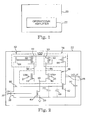
- Figure 1 is a diagram illustrating one embodiment of an electronic system that includes one embodiment of an operational amplifier, according to the present invention.
- Figure 2 is a diagram illustrating one embodiment of an operational amplifier of the present invention.
- Figure 3 is a bode diagram illustrating the overall gain magnitude versus frequency and the overall gain phase versus frequency of one embodiment of an operational amplifier of the present invention.
- FIG. 1 is a diagram illustrating one embodiment of an electronic system 20 that includes one embodiment of an operational amplifier 22, according to the present invention.
- Operational amplifier 22 is a two stage operational amplifier that includes a first gain path configured to provide a low gain and large frequency bandwidth and a second gain path configured to provide a high gain and small frequency bandwidth.
- the overall gain frequency response includes a first pole, a second pole at a higher frequency than the first pole, and a zero.
- Operational amplifier 22 is configured to introduce the zero into its frequency response, without introducing a third pole.
- the stability margin of operational amplifier 22 and/or electronic system 20 is improved and the stability margin improvement is achieved without the use of a large compensation capacitor.
- electronic system 20 includes a feedback loop and operational amplifier 22 is part of the feedback loop such that the zero is used to cancel the first non-dominant pole of the feedback loop system.
- operational amplifier 22 is part of the feedback loop such that the zero is used to cancel the first non-dominant pole of the feedback loop system.
- electronic system 20 is an advanced memory buffer (AMB) circuit.
- AMB advanced memory buffer
- electronic system 20 can be any suitable system that includes an operational amplifier, such as operational amplifier 22.
- Operation amplifier 22 is a two stage operational amplifier that provides an improved stability margin and a gain that can be much higher than the gain of a single stage operational amplifier.
- operational amplifier 22 includes a differential pair of transistors configured to receive differential inputs. The differential pair of transistors direct current through a first current mirror and a second current mirror based on the received differential input signals. The first current mirror provides a first current to one high impedance node and the second current mirror provides a second current to the other high impedance node.
- Figure 2 is a diagram illustrating one embodiment of operational amplifier 22.
- the system is electrically coupled to inverting or negative input 24, non-inverting or positive input 26, and/or output 28.
- Operational amplifier 22 is biased via bias voltage signal VB at bias voltage input 30 and receives negative input signal VIN- at 24 and positive input signal VIN+ at 26.
- Operational amplifier 22 provides output signal VOUT at 28.
- the gain frequency response of operational amplifier 22 includes a zero, without introducing a third pole, and the stability margin of operational amplifier 22 and/or the system that includes operation amplifier 22 is improved without the use of a large compensation capacitor.
- Operational amplifier 22 includes a first current mirror 32, a second current mirror 34, a differential pair of input transistors 36, a transistor 38, a bias transistor 40, and an output transistor 42.
- Each of the transistors of transistor 38, bias transistor 40, and output transistor 42 is an n-channel metal oxide semiconductor (NMOS) transistor.
- the differential pair of input transistors 36 includes a first input transistor 44 and a second input transistor 46.
- Each of the transistors of first input transistor 44 and second input transistor 46 is an NMOS transistor.
- first input transistor 44 is electrically coupled to negative input 24.
- the gate of second input transistor 46 is electrically coupled to positive input 26.
- One side of the drain-source path of first input transistor 44 is electrically coupled to one side of the drain-source path of second input transistor 46 and one side of the drain-source path of bias transistor 40 at 48.
- the other side of the drain-source path of bias transistor 40 is electrically coupled to a reference, such as ground, at 50.
- the gate of bias transistor 40 is electrically couple to bias voltage input 30 to receive bias voltage VB at 30.
- First current mirror 32 includes a first current mirror transistor 52 and a second current mirror transistor 54.
- Each of the transistors of first current mirror transistor 52 and second current mirror transistor 54 is a p-channel metal oxide semiconductor (PMOS) transistor.
- One side of the drain-source path of first current mirror transistor 52 is electrically coupled to power VDD at 56.
- the other side of the drain-source path of first current mirror transistor 52 is electrically coupled at 58 to the other side of the drain-source path of first input transistor 44, the gate of first current mirror transistor 52, and the gate of second current mirror transistor 54.
- One side of the drain-source path of second current mirror transistor 54 is electrically coupled to power VDD at 56.
- the other side of the drain-source path of second current mirror transistor 54 is electrically coupled at 60 to one side of the drain-source path of transistor 38 and the gate of output transistor 42.
- the other side of the drain-source path of transistor 38 is electrically coupled to the reference at 50.
- the gate of transistor 38 is electrically couple to bias voltage input 30 to receive bias voltage VB at 30.
- Second current mirror 34 includes a third current mirror transistor 62 and a fourth current mirror transistor 64.
- Each of the transistors of third current mirror transistor 62 and fourth current mirror transistor 64 is a PMOS transistor.
- One side of the drain-source path of third current mirror transistor 62 is electrically coupled to power VDD at 56.
- the other side of the drain-source path of third current mirror transistor 62 is electrically coupled at 66 to the other side of the drain-source path of second input transistor 46, the gate of third current mirror transistor 62, and the gate of fourth current mirror transistor 64.
- One side of the drain-source path of fourth current mirror transistor 64 is electrically coupled to power VDD at 56.
- the other side of the drain-source path of fourth current mirror transistor 64 is electrically coupled at 28 to one side of the drain-source path of output transistor 42.
- the other side of the drain-source path of output transistor 42 is electrically coupled to the reference at 50.
- the input to output ratio of each of the two current mirrors 32 and 34 is 1. In other embodiments, the input to output ratio of first current mirror 32 is any suitable value and the input to output ratio of second current mirror 34 is any suitable value.
- Operational amplifier 22 includes a first capacitor 68, a second capacitor 70, and a parasitic capacitor 72, indicated in dashed lines.
- One side of first capacitor 68 and one side of parasitic capacitor 72 are electrically coupled at 60 to the gate of output transistor 42.
- the other side of first capacitor 68 and the other side of parasitic capacitor 72 are electrically coupled to the reference at 50.
- one side of second capacitor 70 is electrically coupled at 28 to one side of the drain-source path of output transistor 42, and the other side of second capacitor 70 is electrically coupled to the reference at 50.
- bias transistor 40 receives bias voltage VB at 30 and provides bias to the differential pair of input transistors 36. Also, transistor 38 receives bias voltage VB at 30 and provides a first high impedance node at 60. The gate of output transistor 42 receives a signal via the first high impedance node at 60 to control output transistor 42. Output 28 provides a second high impedance node at 28. In one embodiment, transistor 38 is smaller than bias transistor 40.
- First input transistor 44 receives negative input signal VIN- at 24 and second input transistor 46 receives positive input signal VIN+ at 26. If negative input signal VIN- at 24 is greater or more positive than positive input signal VIN+ at 26, the current through first input transistor 44 is larger than the current through second input transistor 46.
- the differential input transistors 36 steer more current through first current mirror 32 and first current mirror transistor 52 than through second current mirror 34 and third current mirror transistor 62, which reduces the current flowing through fourth current mirror transistor 64.
- the current through first current mirror transistor 52 is mirrored through second current mirror transistor 54 and first high impedance node 60 is charged to a higher voltage level that makes output transistor 42 more conductive.
- Second input transistor 46 is more conductive than first input transistor 44.
- the differential input transistors 36 steer more current through second current mirror 34 and third current mirror transistor 62 than through first current mirror 32 and first current mirror transistor 52, which reduces the current flowing through second current mirror transistor 54.
- Transistor 38 discharges the first high impedance node 60 to a lower voltage level, which makes output transistor 42 less conductive and reduces the drain current through output transistor 42.
- the current through third current mirror transistor 62 is mirrored through fourth current mirror transistor 64 and the reduced drain current through output transistor 42 in combination with the increased current through fourth current mirror transistor 64 charges second high impedance node 28 to a higher voltage level and provides the higher voltage level in output signal VOUT at 28.
- output signal VOUT is higher.
- Operational amplifier 22 is a two stage operational amplifier that includes a first gain path and a second gain path.
- the first gain path is a low gain and large bandwidth path.
- the second gain path is a high gain and low or small bandwidth path.
- the input to output ratio of each of the two current mirrors 32 and 34 is 1.
- the input to output ratio of first current mirror 32 can be any suitable value and the input to output ratio of second current mirror 34 can be any suitable value.
- Equation I The overall gain of operational amplifier 22 is given by Equation I.
- A g ⁇ m 36 * R ⁇ o ⁇ u ⁇ t 28 1 + j ⁇ ⁇ ⁇ C 70 ⁇ R ⁇ o ⁇ u ⁇ t 28 ) * ( g ⁇ m 42 * R ⁇ o ⁇ u ⁇ t 60 1 + j ⁇ ⁇ ⁇ R ⁇ o ⁇ u ⁇ t 60 ⁇ C 68 + C 72 + 1
- gm36 is the transconductance of first and second input transistors 44 and 46
- ROUT60 is the equivalent resistance at first high impedance node 60
- C68 is the capacitance of first capacitor 68
- C72 is the capacitance of parasitic capacitor 72 connected to first high impedance node 60
- gm42 is the transconductance of output transistor 42
- C70 is the capacitance of second capacitor 70
- ROUT28 is the equivalent resistance at second high impedance node 28.
- the overall gain of operational amplifier 22, given by Equation I, includes the first gain path's low gain and large bandwidth term, given by Equation II, and the second gain path's high gain and small bandwidth term, given by Equation III.
- the overall gain of operational amplifier 22 includes a first pole fP1, given by Equation IV, and a second pole fP2, given by Equation V.
- a third pole due to parasitic capacitor 72 is avoided because the capacitance C72 of parasitic capacitor 72 adds up directly to the capacitance C68 of first capacitor 68.
- f P ⁇ 1 1 2 ⁇ ⁇ ⁇ R ⁇ o ⁇ u ⁇ t 60 ⁇ C 68 + C 72
- f P ⁇ 2 1 2 ⁇ ⁇ ⁇ R ⁇ o ⁇ u ⁇ t 28 ⁇ C 70
- the overall gain of operational amplifier 22 includes a zero fZ0, given by Equation VI, where the approximated expression of fZ0 is valid if the product of ROUT60 and gm42 is greater than one.
- f Z ⁇ 0 1 + g ⁇ m 42 ⁇ R ⁇ o ⁇ u ⁇ t 60 2 ⁇ ⁇ ⁇ R ⁇ o ⁇ u ⁇ t 60 ( C 68 + C 72 ) ⁇ g ⁇ m 42 2 ⁇ ⁇ ⁇ C 68 + C 72
- Operational amplifier 22 is a two stage operational amplifier that includes a first gain path that provides a low gain and large frequency bandwidth and a second gain path that provides a high gain and small frequency bandwidth.
- the overall gain frequency response includes a first pole at frequency fP1, a second pole at frequency fP2, and a zero at frequency fZ0, without introducing a third pole.
- the values of gm42 and capacitance C68 are picked to position zero fZ0 substantially next to or close to the first non-dominant pole.
- the first non-dominant pole is a pole, such as second pole fP2 or another pole in the system that includes operational amplifier 22.
- Figure 3 is a bode diagram illustrating the overall gain magnitude versus frequency at 100 and the overall gain phase versus frequency at 102 of one embodiment of operational amplifier 22.
- the overall gain magnitude at 100 is at a maximum value at 104 and the overall gain phase is at 0 degrees at 106.
- the overall gain phase at 102 transitions toward 90 degrees at 110.
- the overall gain magnitude at 100 decreases at 112 and the overall gain phase at 102 transitions to 90 degrees at 114.
- the overall gain phase at 102 increases at 120.
- the overall gain magnitude at 100 stops decreasing to provide the flat overall gain at 118.
- the overall gain magnitude at 100 decreases at 124.
- the overall gain phase at 102 returns to a 90 degree phase at 126.
- the zero fZ0 at 116 is positioned substantially next to the second pole fP2 at 122 and the overall gain phase at 102 remains substantially at 90 degrees at frequencies beyond the first pole fP1 to stabilize operational amplifier 22.
- the zero fZ0 at 116 can be situated substantially at the second pole fP2 at 122 or at a higher frequency than second pole fP2 at 122, but substantially next to the second pole fP2 at 122 to provide a sufficient phase margin for the overall loop gain. In other embodiments, the zero fZ0 at 116 can be positioned substantially next to the first non-dominant pole of a system that includes operational amplifier 22 to improve the stability of the system.
- Operational amplifier 22 is a two stage operational amplifier that provides a gain magnitude, which can be much larger than the gain magnitude of a single stage operational amplifier.
- Operational amplifier 22 provides an overall gain response that includes a first pole fP1, a second pole fP2 at a higher frequency than the first pole fP1, and a zero fZ0 .
- the zero fZ0 is positioned substantially next to the second pole fP2 and the overall gain phase remains substantially at 90 degrees at frequencies beyond the first pole fP1. As a result, the stability margin of operational amplifier 22 is improved.
Landscapes
- Engineering & Computer Science (AREA)
- Power Engineering (AREA)
- Amplifiers (AREA)
Applications Claiming Priority (1)
| Application Number | Priority Date | Filing Date | Title |
|---|---|---|---|
| US11/411,388 US20070252648A1 (en) | 2006-04-26 | 2006-04-26 | Operational amplifier |
Publications (2)
| Publication Number | Publication Date |
|---|---|
| EP1850477A2 true EP1850477A2 (fr) | 2007-10-31 |
| EP1850477A3 EP1850477A3 (fr) | 2007-11-28 |
Family
ID=38279234
Family Applications (1)
| Application Number | Title | Priority Date | Filing Date |
|---|---|---|---|
| EP07106708A Withdrawn EP1850477A3 (fr) | 2006-04-26 | 2007-04-23 | Amplificateur opérationnel |
Country Status (5)
| Country | Link |
|---|---|
| US (1) | US20070252648A1 (fr) |
| EP (1) | EP1850477A3 (fr) |
| JP (1) | JP2007295566A (fr) |
| KR (1) | KR20070105907A (fr) |
| CN (1) | CN101072014A (fr) |
Families Citing this family (5)
| Publication number | Priority date | Publication date | Assignee | Title |
|---|---|---|---|---|
| US8395448B2 (en) * | 2011-01-14 | 2013-03-12 | Analog Devices, Inc. | Apparatus and method for miller compensation for multi-stage amplifier |
| CN102510267B (zh) * | 2011-12-28 | 2015-01-14 | 上海贝岭股份有限公司 | 一种二级运算放大器电路 |
| CN108521268A (zh) * | 2018-03-05 | 2018-09-11 | 华南理工大学 | 一种快速起振的晶体振荡器、电子系统和方法 |
| US10461706B1 (en) | 2018-04-30 | 2019-10-29 | Texas Instruments Incorporated | Differential amplifier including cancellation capacitors |
| US11431334B2 (en) | 2020-04-06 | 2022-08-30 | Analog Devices International Unlimited Company | Closed loop switch control system and method |
Family Cites Families (25)
| Publication number | Priority date | Publication date | Assignee | Title |
|---|---|---|---|---|
| US3619797A (en) * | 1970-01-21 | 1971-11-09 | Globe Universal Sciences | Operational amplifier |
| US4379267A (en) * | 1980-06-25 | 1983-04-05 | Mostek Corporation | Low power differential amplifier |
| US4933644A (en) * | 1988-12-23 | 1990-06-12 | Texas Instruments, Incorporated | Common-mode feedback bias generator for operational amplifiers |
| US4959622A (en) * | 1989-08-31 | 1990-09-25 | Delco Electronics Corporation | Operational amplifier with precise bias current control |
| US5132560A (en) * | 1990-09-28 | 1992-07-21 | Siemens Corporate Research, Inc. | Voltage comparator with automatic output-level adjustment |
| US5373248A (en) * | 1993-06-08 | 1994-12-13 | At&T Bell Laboratories | Transconductor employing differential pair composite field effect transistors |
| US5374897A (en) * | 1993-10-21 | 1994-12-20 | National Semiconductor Corporation | Balanced, high-speed differential input stage for Op-amps |
| US5406220A (en) * | 1993-11-01 | 1995-04-11 | Motorola Inc. | Pole/zero compensation in cascode amplifiers |
| DE69325810T2 (de) * | 1993-11-30 | 1999-11-18 | Stmicroelectronics S.R.L., Agrate Brianza | CMOS-integrierter Hochleistungs-Transkonduktanz-Operationsverstärker |
| GB2295932B (en) * | 1994-12-08 | 1999-04-14 | Motorola Inc | Two-stage operational amplifier circuit |
| DE19533768C1 (de) * | 1995-09-12 | 1996-08-29 | Siemens Ag | Stromtreiberschaltung mit Querstromregelung |
| SG52763A1 (en) * | 1996-05-16 | 1998-09-28 | Inst Of Microelectronics | Low-voltage multipath-miller-zero-compensated cmos class-ab operational amplifier |
| US5838199A (en) * | 1996-05-28 | 1998-11-17 | Analog Devices, Inc. | Multi-stage high-performance amplifier |
| US6002299A (en) * | 1997-06-10 | 1999-12-14 | Cirrus Logic, Inc. | High-order multipath operational amplifier with dynamic offset reduction, controlled saturation current limiting, and current feedback for enhanced conditional stability |
| US6084475A (en) * | 1998-10-06 | 2000-07-04 | Texas Instruments Incorporated | Active compensating capacitive multiplier |
| US6476675B1 (en) * | 2000-08-11 | 2002-11-05 | Globespanvirata, Inc. | Double-cascode two-stage operational amplifier |
| FR2822308B1 (fr) * | 2001-03-19 | 2003-06-13 | St Microelectronics Sa | Circuit pour la separation de poles reposant sur l'effet miller |
| US6556077B2 (en) * | 2001-03-20 | 2003-04-29 | Texas Instruments Incorporated | Instrumentation amplifier with improved AC common mode rejection performance |
| JP2005512378A (ja) * | 2001-12-03 | 2005-04-28 | コーニンクレッカ フィリップス エレクトロニクス エヌ ヴィ | 増幅器を備えた集積回路 |
| US6831513B2 (en) * | 2002-01-16 | 2004-12-14 | Oki Electric Industry Co., Ltd. | Differential amplifier |
| US7013118B2 (en) * | 2002-03-25 | 2006-03-14 | Broadcom Corporation | High speed operational amplifier design |
| US6586997B1 (en) * | 2002-01-30 | 2003-07-01 | Analog Devices, Inc. | Input distortion correction current-feedback amplifier system |
| US6724260B2 (en) * | 2002-03-28 | 2004-04-20 | Texas Instruments Incorporated | Low power current feedback amplifier |
| US6734737B2 (en) * | 2002-06-12 | 2004-05-11 | Analog Devices, Inc. | Output distortion correction amplifier system |
| US6965268B2 (en) * | 2003-08-26 | 2005-11-15 | Intel Corporation | Common mode feedback circuit for fully differential two-stage operational amplifiers |
-
2006
- 2006-04-26 US US11/411,388 patent/US20070252648A1/en not_active Abandoned
-
2007
- 2007-04-19 JP JP2007110201A patent/JP2007295566A/ja not_active Abandoned
- 2007-04-23 EP EP07106708A patent/EP1850477A3/fr not_active Withdrawn
- 2007-04-26 KR KR1020070040820A patent/KR20070105907A/ko not_active Ceased
- 2007-04-26 CN CNA2007101053082A patent/CN101072014A/zh active Pending
Also Published As
| Publication number | Publication date |
|---|---|
| JP2007295566A (ja) | 2007-11-08 |
| US20070252648A1 (en) | 2007-11-01 |
| EP1850477A3 (fr) | 2007-11-28 |
| CN101072014A (zh) | 2007-11-14 |
| KR20070105907A (ko) | 2007-10-31 |
Similar Documents
| Publication | Publication Date | Title |
|---|---|---|
| US7605650B2 (en) | Switched capacitor amplifier with higher gain and improved closed-loop gain accuracy | |
| US7633338B1 (en) | Compensation circuit for amplifiers having multiple stages | |
| US7187235B2 (en) | Class AB rail-to-rail operational amplifier | |
| US7495422B2 (en) | Area-efficient capacitor-free low-dropout regulator | |
| US7268524B2 (en) | Voltage regulator with adaptive frequency compensation | |
| US7030686B2 (en) | Constant voltage circuit with phase compensation | |
| US6741129B1 (en) | Differential amplifier slew rate boosting scheme | |
| US6359510B1 (en) | Amplifier circuit | |
| US5381112A (en) | Fully differential line driver circuit having common-mode feedback | |
| US20070013438A1 (en) | Chopper-stabilized operational amplifier and method | |
| JPH0629761A (ja) | 同相モード安定性が強化された差動増幅器 | |
| JPH077340A (ja) | 全差動増幅器 | |
| US7633346B2 (en) | Transconductance compensating bias circuit and amplifier | |
| EP1850477A2 (fr) | Amplificateur opérationnel | |
| US20170170795A1 (en) | Differential amplifier with common mode compensation circuit | |
| US6972623B2 (en) | Differential amplifier without common mode feedback | |
| US6653895B1 (en) | Gain-boost nulling amplifier for auto-zero circuit | |
| KR20040032589A (ko) | 자기 발진 주파수를 높이기 위한 위상 진상-지상 보상기를구비하는 디지털 오디오 증폭기 | |
| CN108121391B (zh) | 用于进行自偏置且自调节共模放大的方法和设备 | |
| US7528658B2 (en) | Threshold voltage compensation for a two stage amplifier | |
| EP1435693B1 (fr) | Circuit d'amplification | |
| US7248117B1 (en) | Frequency compensation architecture for stable high frequency operation | |
| US7586349B2 (en) | CMOS integrated circuit for correction of duty cycle of clock signal | |
| US7295068B2 (en) | Increasing the linearity of a transconductance cell | |
| US20190199304A1 (en) | Operational amplifier |
Legal Events
| Date | Code | Title | Description |
|---|---|---|---|
| PUAI | Public reference made under article 153(3) epc to a published international application that has entered the european phase |
Free format text: ORIGINAL CODE: 0009012 |
|
| PUAL | Search report despatched |
Free format text: ORIGINAL CODE: 0009013 |
|
| AK | Designated contracting states |
Kind code of ref document: A2 Designated state(s): AT BE BG CH CY CZ DE DK EE ES FI FR GB GR HU IE IS IT LI LT LU LV MC MT NL PL PT RO SE SI SK TR |
|
| AX | Request for extension of the european patent |
Extension state: AL BA HR MK YU |
|
| AK | Designated contracting states |
Kind code of ref document: A3 Designated state(s): AT BE BG CH CY CZ DE DK EE ES FI FR GB GR HU IE IS IT LI LT LU LV MC MT NL PL PT RO SE SI SK TR |
|
| AX | Request for extension of the european patent |
Extension state: AL BA HR MK YU |
|
| 17P | Request for examination filed |
Effective date: 20080307 |
|
| 17Q | First examination report despatched |
Effective date: 20080404 |
|
| AKX | Designation fees paid |
Designated state(s): DE FR GB |
|
| STAA | Information on the status of an ep patent application or granted ep patent |
Free format text: STATUS: THE APPLICATION IS DEEMED TO BE WITHDRAWN |
|
| 18D | Application deemed to be withdrawn |
Effective date: 20080815 |