EP1850141A2 - Apparatus and method for processing signals between a tester and a plurality of devices under test at high temperatures and with single touchdown of a probe array - Google Patents
Apparatus and method for processing signals between a tester and a plurality of devices under test at high temperatures and with single touchdown of a probe array Download PDFInfo
- Publication number
- EP1850141A2 EP1850141A2 EP07008318A EP07008318A EP1850141A2 EP 1850141 A2 EP1850141 A2 EP 1850141A2 EP 07008318 A EP07008318 A EP 07008318A EP 07008318 A EP07008318 A EP 07008318A EP 1850141 A2 EP1850141 A2 EP 1850141A2
- Authority
- EP
- European Patent Office
- Prior art keywords
- under test
- devices under
- tester
- multichip module
- micro
- Prior art date
- Legal status (The legal status is an assumption and is not a legal conclusion. Google has not performed a legal analysis and makes no representation as to the accuracy of the status listed.)
- Withdrawn
Links
Images


Classifications
-
- H—ELECTRICITY
- H01—ELECTRIC ELEMENTS
- H01L—SEMICONDUCTOR DEVICES NOT COVERED BY CLASS H10
- H01L22/00—Testing or measuring during manufacture or treatment; Reliability measurements, i.e. testing of parts without further processing to modify the parts as such; Structural arrangements therefor
-
- G—PHYSICS
- G01—MEASURING; TESTING
- G01R—MEASURING ELECTRIC VARIABLES; MEASURING MAGNETIC VARIABLES
- G01R31/00—Arrangements for testing electric properties; Arrangements for locating electric faults; Arrangements for electrical testing characterised by what is being tested not provided for elsewhere
- G01R31/28—Testing of electronic circuits, e.g. by signal tracer
- G01R31/2851—Testing of integrated circuits [IC]
- G01R31/2886—Features relating to contacting the IC under test, e.g. probe heads; chucks
- G01R31/2889—Interfaces, e.g. between probe and tester
Definitions
- Mechanical relays are also quite expensive. For example, the typical mechanical relays may each cost about $8.00. This may limit the return on investment (ROI) for the customer. Mechanical relays are generally rated for about 1 to 10 million test cycles. This may create reliability issues for the customer over time. Furthermore, mechanical relays are only rated for operation up to 85° C. This allows testing of NAND devices using mechanical relays at or below 85° C.
- ROI return on investment
- apparatus for processing signals between a tester and a plurality of devices under test, the apparatus comprising at least one multichip module, each of the at least one multichip module comprising a plurality of micro-electromechanical switches between a first set of connectors to the tester and a second set of connectors to the plurality of devices under test; and at least one driver to selectively operate each of the plurality of micro-electromechanical switches.
- a system for testing a plurality of devices under test comprising a set of tester electronics to generate signals for application to the plurality of devices under test, and to receive signals generated by the plurality of devices under test; a probe card with at least one multichip module mounted thereon, each of the at least one multichip module comprising a plurality of micro-electromechanical switches between a first set of connectors to the set of tester electronics and a second set of connectors to the plurality of devices under test, and a driver to selectively operate each of the plurality of micro-electromechanical switches; and a probe array to transmit signals between the at least one multichip module of the probe card and the plurality of devices under test.
- apparatus for processing signals between a tester and a plurality of devices under test comprising at least one multichip module mounted directly on a probe card and operable at a temperature of at least 125° C, and each of the at least one multichip module having a plurality of micro-electromechanical switches between a first set of connectors to the tester and a second set of connectors to the plurality of devices under test.
- a method of processing signals between a tester and a plurality of devices under test comprising connecting the tester and the plurality of devices under test with at least one multichip module, each of the at least one multichip module having a plurality of micro-electromechanical switches between a first set of connectors to the tester and a second set of connectors to the plurality of devices under test; and selectively operating each of the plurality of micro-electromechanical switches.
- FIGURES 1-3 illustrate one exemplary embodiment of a multichip module for processing signals between a tester and a plurality of devices under test
- FIGURE 4 illustrates a system having a probe card with a plurality of multichip modules for processing signals between a tester and a plurality of devices under test;
- FIGURES 5-7 illustrate another exemplary embodiment of a multichip module for processing signals between a tester and a plurality of devices under test.
- FIGURE 8 is a flow chart diagram illustrative of methods of processing signals between a tester and a plurality of devices under test.
- apparatus 100 for processing signals may include a configuration in which each of multichip modules 102 are mounted directly on a probe card 112. Due to the proximity of multichip modules 102 to probe card 112 and the devices under test (not shown), one or more of multichip modules 102 may operate at a speed of at least 100 MHz. In another embodiment, one or more of multichip modules 102 may operate at a speed above 20 MHz to about 100 MHz.
- one or more of multichip modules 102 may be rated for at least 1 billion test cycles. Multichip modules 102 may be rated for 10 billion or more test cycles. This is due, at least in part, to the micro-electromechanical switches 104 that may be used instead of other types of switches.
- MEM MCM 102 may be attached to probe card 112 using screws 120 or other fasteners, a new tester does not need to be purchased from a supplier of the ATE system. A customer may simply design a probe care and attach these MEM MCMs to the probe card and install this new probe card assembly onto an existing ATE system.
- one or more of drivers 110 may designed to supply an electrostatic potential to selectively activate a MEMs gate associated with one or more of the plurality of micro-electromechanical switches 104.
- One or more of drivers 110 may be a vacuum-florescent display driver die 110.
- four drivers 110 (FIGURE 2) act as an algorithmic pattern generating system (APGS) and supply the electrostatic potential to four separate DUTs independently of one another.
- one driver 110 (FIGURE 6) acts as an algorithmic pattern generating system (APGS) and supplies electrostatic potential to DUTs.
- the second set of connectors of multichip modules 102 attach to a probe array 122.
- This probe array 122 may have at least 6000 probe tip needles so as to test at least 6000 test sites of the plurality of devices under test during a single touchdown of probe array 122.
- each multichip module 102 may test 12 DUTs, there may be 36 multichip modules in attachment to probe card 112 for a total of 432 DUTs, and there may be 16 test sites on each one of the DUTs for a total of 6912 test sites, which in turn requires 6912 probe tip needles.
- System 124 may include a set of tester electronics 126 to generate signals for application to the plurality of devices under test, and to receive signals generated by the plurality of devices under test.
- System 124 may include probe card 112 with at least one multichip module 102 mounted directly on probe card 112.
- Each of the at least one multichip module 102 may include a plurality of micro-electromechanical switches 104 between a first set of connectors to the set of tester electronics 126 and a second set of connectors to the plurality of devices under test.
- System may include one or more drivers 110 to selectively operate each of the plurality of micro-electromechanical switches 104.
- System 124 may further include probe array 122 to transmit signals between the multichip modules 102 of probe card 112 and the plurality of devices under test.
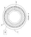
- Probe card 112 may have a maximum diameter of 440 millimeters. Probe card 112 may form an opening 128 for probe array 122. In an embodiment, opening 128 has a minimum diameter of 330 millimeters. Probe card 112 may contains at least 36 of multichip modules 102 mounted thereon.
- probe array 112 may have at least 6000 probe tip needles so as to test at least 6000 test sites of the plurality of devices under test during a single touchdown of probe array 112.
- system 124 enables one touchdown testing of 300 mm wafers containing NAND devices to be tested up to 100 MHz by mounting micro-electromechanical multichip modules 102 very close to the DUTs. This one touchdown testing cannot be achieved by using mechanical relays or active silicon devices mounted on daughter boards. Daughter boards mounted on the probe cannot achieve the required density of switches because of the space required for connectors. Mechanical relays, which are mounted far from the DUTs, are generally limited to about 20 MHz and cannot achieve a data rate near 100 MHz.
- MCM multichip module
- MCM multichip module
- MEM MCMs 102 may be fabricated quite inexpensively. For example, an MCM package containing 128 SPDT switches with only 780 pins may cost about $300 per package. This drastically improves the return on investment (ROI) for the customer.
- ROI return on investment
- NAND devices may only be tested up to 85° C. However, using system 100, NAND devices may be tested at temperatures ranging from -40° C to 125° C with one or more of MEM MCMs 102.
- MEM MCMs 102 are generally mounted very close to the DUTs so as to increase the maximum data rate for testing NAND devices from 20 MHz to 100 MHz, and also to enable testing of the entire 300 mm wafer with one touchdown.
- MEM MCMs 102 Utilizing MEM MCMs 102 instead of mechanical relays is also more cost effective and more reliable.
- a typical mechanical relay is rated for 1-10 million cycles.
- a typical MEM MCM 102 may be rated for 1-10 billion cycles.
- Using daughter boards limits the density of switches that can be mounted on the probe card due to the space required for connectors.
- Multichip modules 102 are generally capable of much higher densities than daughter cards. Mounting multichip modules 102 onto probe card 112 enables the customer to double the pin count of the test system when testing NAND devices without buying a new ATE system.
- MCM substrate 102B may be a blind and buried via substrate made of NELCO 4000-13 Si, which is a typical MCM substrate.
- Connectors 106 and connectors 108 may include, but are not limited to pins. Such pins of the package may include Be-Cu springs that are attached with silver epoxy to the bottom of the NELCO 4000-13 Si substrate.
- MEMs 104 and single VFD 110 may be located inside MCM 102 and may be wired bond or soldered to the substrate.
- MCMs 102 may be reusable. MCMs 102 can be transferred form one probe card to another when the probe card becomes damaged or is simply obsolete due to a change in die size or layout on the wafers.
- Alignment pins 130 may be provided to align MCM 102 to probe card 112.
- Method 800 may include connecting 802 the tester and the plurality of devices under test with at least one multichip module, each of the at least one multichip module having a plurality of micro-electromechanical switches between a first set of connectors to the tester and a second set of connectors to the plurality of devices under test.
- Method 800 may include selectively operating 804 each of the plurality of micro-electromechanical switches.
- method 800 may further include operating 806 the at least one multichip module at a speed of at least 100 MHz. In an embodiment, method 800 may include operating 808 the multichip module at temperatures from -40° C to 125° C.
- Method 800 may include mounting 810 each of the at least one multichip module directly on the probe card.
Landscapes
- Engineering & Computer Science (AREA)
- Computer Hardware Design (AREA)
- Microelectronics & Electronic Packaging (AREA)
- General Engineering & Computer Science (AREA)
- Physics & Mathematics (AREA)
- General Physics & Mathematics (AREA)
- Manufacturing & Machinery (AREA)
- Power Engineering (AREA)
- Testing Or Measuring Of Semiconductors Or The Like (AREA)
- Tests Of Electronic Circuits (AREA)
Abstract
Description
- Others have developed solutions for two touchdown testing of 300 mm wafers containing many NAND dice, e.g. 432 NAND dice having 16 test sites each for a total of 6912 test sites. Generally, this type of testing utilizes mechanical relays installed in the device under test (DUT) interface of the automatic test equipment (ATE) system. These relays are typically located electrically far away from the device under test (DUT). This distance may create a large impedance mismatch when reading back from the device. In addition, the maximum data rate for testing the device may be limited to only 20 MHz.
- Mechanical relays are also quite expensive. For example, the typical mechanical relays may each cost about $8.00. This may limit the return on investment (ROI) for the customer. Mechanical relays are generally rated for about 1 to 10 million test cycles. This may create reliability issues for the customer over time. Furthermore, mechanical relays are only rated for operation up to 85° C. This allows testing of NAND devices using mechanical relays at or below 85° C.
- Other solutions for multiplexing a large number of tester pin electronics (PE) by mounting a plurality of daughter boards on probe cards. This will only allow two touchdown testing of 300 mm wafers of NAND dice. This daughter card approach has limitations with respect to temperature and density. The connector limits the density of switches that can be placed on the daughter card and the active silicon switches have a temperature limitation of 85° C when using standard grade integrated chips.
- In an embodiment, there is provided apparatus for processing signals between a tester and a plurality of devices under test, the apparatus comprising at least one multichip module, each of the at least one multichip module comprising a plurality of micro-electromechanical switches between a first set of connectors to the tester and a second set of connectors to the plurality of devices under test; and at least one driver to selectively operate each of the plurality of micro-electromechanical switches.
- In another embodiment, there is provided a system for testing a plurality of devices under test, the system comprising a set of tester electronics to generate signals for application to the plurality of devices under test, and to receive signals generated by the plurality of devices under test; a probe card with at least one multichip module mounted thereon, each of the at least one multichip module comprising a plurality of micro-electromechanical switches between a first set of connectors to the set of tester electronics and a second set of connectors to the plurality of devices under test, and a driver to selectively operate each of the plurality of micro-electromechanical switches; and a probe array to transmit signals between the at least one multichip module of the probe card and the plurality of devices under test.
- In yet another embodiment, there is provided apparatus for processing signals between a tester and a plurality of devices under test, the apparatus comprising at least one multichip module mounted directly on a probe card and operable at a temperature of at least 125° C, and each of the at least one multichip module having a plurality of micro-electromechanical switches between a first set of connectors to the tester and a second set of connectors to the plurality of devices under test.
- In still another embodiment, there is provided a method of processing signals between a tester and a plurality of devices under test, the method comprising connecting the tester and the plurality of devices under test with at least one multichip module, each of the at least one multichip module having a plurality of micro-electromechanical switches between a first set of connectors to the tester and a second set of connectors to the plurality of devices under test; and selectively operating each of the plurality of micro-electromechanical switches.
- Other embodiments are also disclosed.
- Illustrative embodiments of the invention are illustrated in the drawings, in which:
- FIGURES 1-3 illustrate one exemplary embodiment of a multichip module for processing signals between a tester and a plurality of devices under test;
- FIGURE 4 illustrates a system having a probe card with a plurality of multichip modules for processing signals between a tester and a plurality of devices under test;
- FIGURES 5-7 illustrate another exemplary embodiment of a multichip module for processing signals between a tester and a plurality of devices under test; and
- FIGURE 8 is a flow chart diagram illustrative of methods of processing signals between a tester and a plurality of devices under test.
- Referring to FIGURES 1-7, there is shown
apparatus 100 for processing signals between a tester and a plurality of devices under test. In one embodiment,apparatus 100 may include various types ofmultichip modules 102, which are also referred to asMCMs 102. FIGURES 1-3 illustrate one exemplary embodiment ofmultichip module 102. FIGURES 4-7 illustrate another exemplary embodiment ofmultichip module 102. - A
top cover 102A ofmultichip module 102 is shown in FIGURES 1 and 5. Across-sectional plan view 102B ofmultichip module 102 is shown in FIGURES 2 and 6. Abottom portion 102C is shown in FIGURES 3 and 6. - Referring to FIGURES 2 and 5, and each
multichip module 102 may include a plurality ofmicro-electromechanical switches 104, which are also refered to asMEMs 104, between a first set ofconnectors 106 to the tester and a second set ofconnectors 108 to the plurality of devices under test. Each multichip module may include at least onedriver 110 to selectively operate each of the plurality ofmicro-electromechanical switches 104. - Looking at FIGURE 4, and in an embodiment,
apparatus 100 for processing signals may include a configuration in which each ofmultichip modules 102 are mounted directly on aprobe card 112. Due to the proximity ofmultichip modules 102 toprobe card 112 and the devices under test (not shown), one or more ofmultichip modules 102 may operate at a speed of at least 100 MHz. In another embodiment, one or more ofmultichip modules 102 may operate at a speed above 20 MHz to about 100 MHz. - In an embodiment, one or more of
multichip modules 102 may operate at a temperature with a range from about -40° C to about 125° C. In another embodiment, one or more ofmultichip modules 102 may operate within a temperature range from about 85° C to about 125° C. - In one embodiment, one or more of
multichip modules 102 may be rated for at least 1 billion test cycles.Multichip modules 102 may be rated for 10 billion or more test cycles. This is due, at least in part, to themicro-electromechanical switches 104 that may be used instead of other types of switches. - Referring to FIGURES 2 and 6, and in an embodiment, the plurality of
micro-elecromechanical switches 104 may be housed inseparate MEMs dice 114. In one embodiment, each of theseparate MEMs dice 114 may include eight single pole triple throw switches (FIGURE 2). In another embodiment, each of theseparate MEMs dice 114 may include eight single pole double throw switches (FIGURE 6). - Looking at FIGURES 1-3 and 5-7, an
attachment component 116 may be provided to secure one or more ofmultichip modules 102. In an embodiment,attachment component 116mounts multichip module 102 to probe card 112 (FIGURE 4).Attachment component 116 may includepassageways 118 throughmultichip module 102 for a set ofscrews 120 to mount the multchip module to probe card 112 (FIGURE 4). - As MEM MCM 102 may be attached to
probe card 112 usingscrews 120 or other fasteners, a new tester does not need to be purchased from a supplier of the ATE system. A customer may simply design a probe care and attach these MEM MCMs to the probe card and install this new probe card assembly onto an existing ATE system. - Generally, MCM 102 may be very thin to allow
probe card 112 together withMCMs 102 to fit into an auto loader of a prober.Many screws 120 or other fasteners may be used to attach MCM 102 toprobe card 112 to prevent warping. - In an embodiment, one or more of
drivers 110 may designed to supply an electrostatic potential to selectively activate a MEMs gate associated with one or more of the plurality ofmicro-electromechanical switches 104. One or more ofdrivers 110 may be a vacuum-florescent display driver die 110. In one embodiment, four drivers 110 (FIGURE 2) act as an algorithmic pattern generating system (APGS) and supply the electrostatic potential to four separate DUTs independently of one another. In another embodiment, one driver 110 (FIGURE 6) acts as an algorithmic pattern generating system (APGS) and supplies electrostatic potential to DUTs. - In one embodiment, the second set of connectors of
multichip modules 102 attach to aprobe array 122. Thisprobe array 122 may have at least 6000 probe tip needles so as to test at least 6000 test sites of the plurality of devices under test during a single touchdown ofprobe array 122. For example, eachmultichip module 102 may test 12 DUTs, there may be 36 multichip modules in attachment toprobe card 112 for a total of 432 DUTs, and there may be 16 test sites on each one of the DUTs for a total of 6912 test sites, which in turn requires 6912 probe tip needles. - Referring to FIGURE 4, and in an embodiment, there is shown a
system 124 for testing a plurality of devices under test.System 124 may include a set oftester electronics 126 to generate signals for application to the plurality of devices under test, and to receive signals generated by the plurality of devices under test.System 124 may includeprobe card 112 with at least onemultichip module 102 mounted directly onprobe card 112. Each of the at least onemultichip module 102 may include a plurality ofmicro-electromechanical switches 104 between a first set of connectors to the set oftester electronics 126 and a second set of connectors to the plurality of devices under test. System may include one ormore drivers 110 to selectively operate each of the plurality ofmicro-electromechanical switches 104.System 124 may further includeprobe array 122 to transmit signals between themultichip modules 102 ofprobe card 112 and the plurality of devices under test. - In one embodiment,
probe card 112 may have 36multichip modules 102 mounted thereon. Each ofmultichip modules 102 may have a plurality ofMEMS dice 114 thereon. Furthermore, each one of the plurality ofMEMS dice 114 may each contain a plurality ofswitches 104. In one embodiment, switches 104 may include single pole triple throw switches. In another embodiment, switches 104 may include single pole double throw switches. - Looking at FIGURE 1, and in an embodiment, each of
multichip modules 102 may have 9MEMS dice 114 thereon. In one embodiment, each of the 9MEMS dice 114 may have 8 MEMS switches 104. Looking at FIGURE 4, and in another embodiment, each ofmultichip modules 102 may have 16MEMS dice 114 thereon. In an embodiment, each of the 16MEMS dice 114 may have 8 MEMS switches 104. - Referring to FIGURES 3 and 7, and in an embodiment, each one
multichip module 104 may be housed in a standard package configuration having 780 pins which may be configured onbottom portion 102C. A portion of the 780 pins form first set ofconnectors 106, which may provide electrical connection to tester electronics. Another portion of the 780 pins form second set ofconnectors 108, which may provide electrical connection to devices under test. -
Probe card 112 may have a maximum diameter of 440 millimeters.Probe card 112 may form anopening 128 forprobe array 122. In an embodiment, opening 128 has a minimum diameter of 330 millimeters.Probe card 112 may contains at least 36 ofmultichip modules 102 mounted thereon. - In an embodiment,
probe array 112 may have at least 6000 probe tip needles so as to test at least 6000 test sites of the plurality of devices under test during a single touchdown ofprobe array 112. - In an embodiment,
system 124 enables one touchdown testing of 300 mm wafers containing NAND devices to be tested up to 100 MHz by mounting micro-electromechanicalmultichip modules 102 very close to the DUTs. This one touchdown testing cannot be achieved by using mechanical relays or active silicon devices mounted on daughter boards. Daughter boards mounted on the probe cannot achieve the required density of switches because of the space required for connectors. Mechanical relays, which are mounted far from the DUTs, are generally limited to about 20 MHz and cannot achieve a data rate near 100 MHz. - For example, and looking at FIGURES 1-3, to achieve a desired data rate of about 20 MHz to about 100 MHz, 72 single-pole, triple-throw (SPTT) MEM switches 104 and four vacuum-florescent display driver dice (VFD) 110 may be integrated into one 780 pin multichip module (MCM) 102. This
MCM 102 may measure 26 mm x 55 mm x 34 mm x 55 mm (see FIGURE 1). - In one embodiment, and looking at FIGURES 5-7, to achieve a desired data rate of about 20 MHz to about 100 MHz, 128 single-pole, double-throw (SPDT) MEM switches 104 and one vacuum-florescent display driver die (VFD) 110 with 32 outputs may be integrated into one 780 pin multichip module (MCM) 102 . This
MCM 102 may measure 26 mm x 55 mm x 34 mm x 55 mm (see FIGURE 5). -
MEM MCMs 102 may be fabricated quite inexpensively. For example, an MCM package containing 128 SPDT switches with only 780 pins may cost about $300 per package. This drastically improves the return on investment (ROI) for the customer. - As discussed above, mechanical relays are generally rated a maximum testing temperature of 85° C, which is due to the moving parts inside the relay housing. Implementations using active silicon devices are also typically rated for a maximum testing temperature of 85° C. Using either of these, i.e. mechanical relays or daughter boards with active silicon, NAND devices may only be tested up to 85° C. However, using
system 100, NAND devices may be tested at temperatures ranging from -40° C to 125° C with one or more ofMEM MCMs 102. -
MEM MCMs 102 are generally mounted very close to the DUTs so as to increase the maximum data rate for testing NAND devices from 20 MHz to 100 MHz, and also to enable testing of the entire 300 mm wafer with one touchdown. - Utilizing
MEM MCMs 102 instead of mechanical relays is also more cost effective and more reliable. A typical mechanical relay is rated for 1-10 million cycles. Atypical MEM MCM 102 may be rated for 1-10 billion cycles. Using daughter boards limits the density of switches that can be mounted on the probe card due to the space required for connectors. -
Multichip modules 102 are generally capable of much higher densities than daughter cards. Mountingmultichip modules 102 ontoprobe card 112 enables the customer to double the pin count of the test system when testing NAND devices without buying a new ATE system. - Using the Agilent V5400 test system, 16 NAND devices with 36 test sites each may be tested. Each MEMs dice may have 8 SPDT switches. The electrostatic potential required to activate the MEMs gate will be supplied by a vacuum-florescent display driver die 110 located inside the
MCM package 102.MCM substrate 102B may be a blind and buried via substrate made of NELCO 4000-13 Si, which is a typical MCM substrate.Connectors 106 andconnectors 108 may include, but are not limited to pins. Such pins of the package may include Be-Cu springs that are attached with silver epoxy to the bottom of the NELCO 4000-13 Si substrate.MEMs 104 andsingle VFD 110 may be located insideMCM 102 and may be wired bond or soldered to the substrate. - In an embodiment,
MCMs 102 may be reusable.MCMs 102 can be transferred form one probe card to another when the probe card becomes damaged or is simply obsolete due to a change in die size or layout on the wafers. - Alignment pins 130 may be provided to align
MCM 102 to probecard 112. - Looking now at FIGURE 8, and in an embodiment, there is provided a
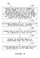
method 800 of processing signals between a tester and a plurality of devices under test.Method 800 may include connecting 802 the tester and the plurality of devices under test with at least one multichip module, each of the at least one multichip module having a plurality of micro-electromechanical switches between a first set of connectors to the tester and a second set of connectors to the plurality of devices under test.Method 800 may include selectively operating 804 each of the plurality of micro-electromechanical switches. - In one embodiment,
method 800 may further include operating 806 the at least one multichip module at a speed of at least 100 MHz. In an embodiment,method 800 may include operating 808 the multichip module at temperatures from -40° C to 125° C. -
Method 800 may include mounting 810 each of the at least one multichip module directly on the probe card.
Claims (10)
- Apparatus (100) for processing signals between a tester and a plurality of devices under test, the apparatus (100) comprising:at least one multichip module (102), each of the at least one multichip module (102) comprising:a plurality of micro-electromechanical switches (104) between a first set of connectors (106) to the tester and a second set of connectors (108) to the plurality of devices under test; andat least one driver (110) to selectively operate each of the plurality of micro-electromechanical switches (104).
- Apparatus (100) in accordance with claim 1, further comprising a probe card (112) on which each one of the at least one multichip module (102) is directly mounted.
- A system in accordance with claim 2, wherein the probe card (112) has a maximum diameter of 440 millimeters.
- A system in accordance with claim 3, wherein the probe card (112) forms an opening (128) for the probe array (122), and the opening (128) has a minimum diameter of 330 millimeters.
- Apparatus (100) in accordance with claim 1, further comprising a plurality of MEMs dice (114) on which the plurality of micro-elecromechanical switches (104) are formed.
- Apparatus (100) in accordance with claim 1, wherein the driver (110) is designed to supply an electrostatic potential to activate a MEMs gate associated with each of the plurality of micro-eledtromechanical switches (104).
- Apparatus (100) in accordance with claim 1, wherein the at least one driver (110) comprises a vacuum-florescent display driver dice (110).
- Apparatus (100) in accordance with claim 1, further comprising a probe array (122) to transmit signals between the at least one multichip module (102) of the probe card (112) and the plurality of devices under test, wherein the probe array (122) has at least 6000 probe tip needles so as to test at least 6000 test sites of the plurality of devices under test during a single touchdown of the probe array (122).
- A method (800) of processing signals between a tester and a plurality of devices under test, the method (800) comprising:connecting (802) the tester and the plurality of devices under test with at least one multichip module, each of the at least one multichip module having a plurality of micro-electromechanical switches between a first set of connectors to the tester and a second set of connectors to the plurality of devices under test; andselectively operating (804) each of the plurality of micro-electromechanical switches.
- A method (800) in accordance with claim 19, further comprising mounting (810) each of the at least one multichip module directly on the probe card, operating (806) the multichip module at a temperature of at least 125° C, and operating (808) the at least one multichip module at a speed of at least 100 MHz.
Applications Claiming Priority (1)
| Application Number | Priority Date | Filing Date | Title |
|---|---|---|---|
| US11/410,699 US7859277B2 (en) | 2006-04-24 | 2006-04-24 | Apparatus, systems and methods for processing signals between a tester and a plurality of devices under test at high temperatures and with single touchdown of a probe array |
Publications (1)
| Publication Number | Publication Date |
|---|---|
| EP1850141A2 true EP1850141A2 (en) | 2007-10-31 |
Family
ID=38353852
Family Applications (1)
| Application Number | Title | Priority Date | Filing Date |
|---|---|---|---|
| EP07008318A Withdrawn EP1850141A2 (en) | 2006-04-24 | 2007-04-24 | Apparatus and method for processing signals between a tester and a plurality of devices under test at high temperatures and with single touchdown of a probe array |
Country Status (6)
| Country | Link |
|---|---|
| US (2) | US7859277B2 (en) |
| EP (1) | EP1850141A2 (en) |
| JP (1) | JP2007292758A (en) |
| KR (1) | KR101342178B1 (en) |
| CN (1) | CN101063704B (en) |
| TW (1) | TWI426281B (en) |
Families Citing this family (10)
| Publication number | Priority date | Publication date | Assignee | Title |
|---|---|---|---|---|
| US7573276B2 (en) * | 2006-11-03 | 2009-08-11 | Micron Technology, Inc. | Probe card layout |
| US20080238461A1 (en) * | 2007-04-02 | 2008-10-02 | Ken Skala | Multi-type test interface system and method |
| US8305098B2 (en) * | 2007-04-26 | 2012-11-06 | Advantest (Singapore) Pte Ltd | Element usable with the method, and a standalone probe card tester formable using the method |
| US7612971B2 (en) * | 2007-06-15 | 2009-11-03 | General Electric Company | Micro-electromechanical system based switching in heating-ventilation-air-conditioning systems |
| WO2009147724A1 (en) * | 2008-06-02 | 2009-12-10 | 株式会社アドバンテスト | Test wafer unit and test system |
| EP2336837B1 (en) * | 2009-12-17 | 2012-09-12 | Electrolux Home Products Corporation N.V. | Electrical assembly for selectively operating a household appliance in a demonstration mode or a standard mode |
| US9733301B2 (en) * | 2010-02-05 | 2017-08-15 | Celerint, Llc | Universal multiplexing interface system and method |
| TWI500945B (en) * | 2013-12-17 | 2015-09-21 | Primax Electronics Ltd | Testing system of circuit board |
| US11266344B2 (en) | 2016-09-21 | 2022-03-08 | Samsung Electronics Co., Ltd. | Method for measuring skin condition and electronic device therefor |
| CN113791251B (en) * | 2021-11-15 | 2022-03-29 | 新恒汇电子股份有限公司 | Method, device and product for detecting failure of SIM card |
Family Cites Families (31)
| Publication number | Priority date | Publication date | Assignee | Title |
|---|---|---|---|---|
| JPH0316930A (en) * | 1989-06-13 | 1991-01-24 | Fujikura Ltd | Production of optical fiber having complicate refractive index distribution |
| KR100384265B1 (en) * | 1994-10-28 | 2003-08-14 | 클리크 앤드 소파 홀딩스 인코포레이티드 | Programmable high-density electronic device testing |
| US5736850A (en) * | 1995-09-11 | 1998-04-07 | Teradyne, Inc. | Configurable probe card for automatic test equipment |
| US5834975A (en) * | 1997-03-12 | 1998-11-10 | Rockwell Science Center, Llc | Integrated variable gain power amplifier and method |
| US6119255A (en) * | 1998-01-21 | 2000-09-12 | Micron Technology, Inc. | Testing system for evaluating integrated circuits, a burn-in testing system, and a method for testing an integrated circuit |
| US6098142A (en) * | 1998-08-25 | 2000-08-01 | Leggett; John D. | Apparatus and method for using a communications port in polling mode and without interrupts |
| US6706546B2 (en) * | 1998-10-09 | 2004-03-16 | Fujitsu Limited | Optical reflective structures and method for making |
| US6499121B1 (en) * | 1999-03-01 | 2002-12-24 | Formfactor, Inc. | Distributed interface for parallel testing of multiple devices using a single tester channel |
| US6657455B2 (en) * | 2000-01-18 | 2003-12-02 | Formfactor, Inc. | Predictive, adaptive power supply for an integrated circuit under test |
| AU2001243200A1 (en) * | 2000-02-22 | 2001-09-03 | Don Mccord | Method and system for wafer and device-level testing of an integrated circuit |
| US6303885B1 (en) * | 2000-03-03 | 2001-10-16 | Optical Coating Laboratory, Inc. | Bi-stable micro switch |
| US6335224B1 (en) * | 2000-05-16 | 2002-01-01 | Sandia Corporation | Protection of microelectronic devices during packaging |
| US6396711B1 (en) * | 2000-06-06 | 2002-05-28 | Agere Systems Guardian Corp. | Interconnecting micromechanical devices |
| US6490536B1 (en) * | 2000-09-14 | 2002-12-03 | Lam Research Corporation | Integrated load simulator |
| US6773962B2 (en) * | 2001-03-15 | 2004-08-10 | General Electric Company | Microelectromechanical system device packaging method |
| DE10112364A1 (en) * | 2001-03-15 | 2002-09-19 | Hilti Ag | Hand tool with electronic depth stop |
| US6492798B2 (en) * | 2001-04-27 | 2002-12-10 | Logicvision, Inc. | Method and circuit for testing high frequency mixed signal circuits with low frequency signals |
| US6762612B2 (en) * | 2001-06-20 | 2004-07-13 | Advantest Corp. | Probe contact system having planarity adjustment mechanism |
| WO2003016930A1 (en) * | 2001-08-10 | 2003-02-27 | Advantest Corporation | Probe module and tester |
| WO2003042094A2 (en) * | 2001-11-09 | 2003-05-22 | Movaz Networks, Inc. | Multi-chip module integrating mems mirror array with electronics |
| US20040016995A1 (en) * | 2002-07-25 | 2004-01-29 | Kuo Shun Meen | MEMS control chip integration |
| US6882256B1 (en) * | 2003-06-20 | 2005-04-19 | Northrop Grumman Corporation | Anchorless electrostatically activated micro electromechanical system switch |
| US7068220B2 (en) * | 2003-09-29 | 2006-06-27 | Rockwell Scientific Licensing, Llc | Low loss RF phase shifter with flip-chip mounted MEMS interconnection |
| TWM253771U (en) * | 2004-03-11 | 2004-12-21 | Chipmos Technologies Inc | Low noise probe head |
| US7305571B2 (en) * | 2004-09-14 | 2007-12-04 | International Business Machines Corporation | Power network reconfiguration using MEM switches |
| US7091765B2 (en) * | 2004-09-30 | 2006-08-15 | International Business Machines Corporation | Circuit power reduction using micro-electromechanical switches |
| US7245134B2 (en) * | 2005-01-31 | 2007-07-17 | Formfactor, Inc. | Probe card assembly including a programmable device to selectively route signals from channels of a test system controller to probes |
| CN101151540B (en) * | 2005-03-31 | 2010-07-21 | 奥克泰克有限公司 | Microstructure probe card, and microstructure inspecting device and method |
| US7285968B2 (en) * | 2005-04-19 | 2007-10-23 | Formfactor, Inc. | Apparatus and method for managing thermally induced motion of a probe card assembly |
| US7504841B2 (en) * | 2005-05-17 | 2009-03-17 | Analog Devices, Inc. | High-impedance attenuator |
| US7924035B2 (en) * | 2008-07-15 | 2011-04-12 | Formfactor, Inc. | Probe card assembly for electronic device testing with DC test resource sharing |
-
2006
- 2006-04-24 US US11/410,699 patent/US7859277B2/en active Active
-
2007
- 2007-04-20 JP JP2007111672A patent/JP2007292758A/en active Pending
- 2007-04-23 KR KR1020070039249A patent/KR101342178B1/en active IP Right Grant
- 2007-04-23 TW TW096114242A patent/TWI426281B/en active
- 2007-04-24 EP EP07008318A patent/EP1850141A2/en not_active Withdrawn
- 2007-04-24 CN CN2007101017137A patent/CN101063704B/en active Active
-
2010
- 2010-12-21 US US12/974,950 patent/US20110089966A1/en not_active Abandoned
Also Published As
| Publication number | Publication date |
|---|---|
| TW200809233A (en) | 2008-02-16 |
| US20110089966A1 (en) | 2011-04-21 |
| KR20070104851A (en) | 2007-10-29 |
| KR101342178B1 (en) | 2013-12-16 |
| CN101063704A (en) | 2007-10-31 |
| US20070247140A1 (en) | 2007-10-25 |
| CN101063704B (en) | 2012-02-08 |
| US7859277B2 (en) | 2010-12-28 |
| TWI426281B (en) | 2014-02-11 |
| JP2007292758A (en) | 2007-11-08 |
Similar Documents
| Publication | Publication Date | Title |
|---|---|---|
| US7859277B2 (en) | Apparatus, systems and methods for processing signals between a tester and a plurality of devices under test at high temperatures and with single touchdown of a probe array | |
| US7046027B2 (en) | Interface apparatus for semiconductor device tester | |
| US6476626B2 (en) | Probe contact system having planarity adjustment mechanism | |
| US7129730B2 (en) | Probe card assembly | |
| TWI424180B (en) | An adaptor frame | |
| JP2014508944A (en) | Equipment for automatic testing / verification of electronic components | |
| US5001422A (en) | VLSI tester backplane | |
| TWI499782B (en) | Stand alone multi-cell probe card for at-speed functional testing | |
| KR20140131481A (en) | Test socket providing mechanical stabilization for pogo pin connections | |
| KR100720788B1 (en) | Device for testing chips by means a printed circuit board | |
| US10962565B2 (en) | Substrate inspection apparatus | |
| US20140253165A1 (en) | Probe card | |
| CN104813172B (en) | Interface for the system of testing | |
| KR100478261B1 (en) | Semiconductor substrate testing apparatus | |
| US7352197B1 (en) | Octal/quad site docking compatibility for package test handler | |
| KR101913274B1 (en) | Probe Card Electrical Characteristic Measuring Device | |
| US7285973B1 (en) | Methods for standardizing a test head assembly | |
| JPH09252031A (en) | Wafer tester | |
| US20240027523A1 (en) | Automatic test equipment | |
| US20240027521A1 (en) | Automatic test equipment | |
| US8203356B2 (en) | Device, system and method for testing and analyzing integrated circuits | |
| US20240027520A1 (en) | Automatic test equipment | |
| KR20090017385A (en) | Apparatus for inspecting electric condition | |
| KR20240013658A (en) | Automatic test equipment and interface equipment thereof | |
| JPH1082825A (en) | Semiconductor inspecting device and method therefor |
Legal Events
| Date | Code | Title | Description |
|---|---|---|---|
| PUAI | Public reference made under article 153(3) epc to a published international application that has entered the european phase |
Free format text: ORIGINAL CODE: 0009012 |
|
| AK | Designated contracting states |
Kind code of ref document: A2 Designated state(s): AT BE BG CH CY CZ DE DK EE ES FI FR GB GR HU IE IS IT LI LT LU LV MC MT NL PL PT RO SE SI SK TR |
|
| AX | Request for extension of the european patent |
Extension state: AL BA HR MK YU |
|
| RIN1 | Information on inventor provided before grant (corrected) |
Inventor name: ANDBERG, JOHN Inventor name: DE LA PUENTE, EDMUNDO Inventor name: MAYDER, ROMI Inventor name: STELLMACHER, PAM |
|
| STAA | Information on the status of an ep patent application or granted ep patent |
Free format text: STATUS: THE APPLICATION IS DEEMED TO BE WITHDRAWN |
|
| 18D | Application deemed to be withdrawn |
Effective date: 20101102 |