EP1840751B1 - Datenverarbeitung mit Datenübertragung zwischen Speichern - Google Patents
Datenverarbeitung mit Datenübertragung zwischen Speichern Download PDFInfo
- Publication number
- EP1840751B1 EP1840751B1 EP07290370A EP07290370A EP1840751B1 EP 1840751 B1 EP1840751 B1 EP 1840751B1 EP 07290370 A EP07290370 A EP 07290370A EP 07290370 A EP07290370 A EP 07290370A EP 1840751 B1 EP1840751 B1 EP 1840751B1
- Authority
- EP
- European Patent Office
- Prior art keywords
- data
- memory
- group
- format
- processing
- Prior art date
- Legal status (The legal status is an assumption and is not a legal conclusion. Google has not performed a legal analysis and makes no representation as to the accuracy of the status listed.)
- Not-in-force
Links
Images

Classifications
-
- G—PHYSICS
- G06—COMPUTING OR CALCULATING; COUNTING
- G06F—ELECTRIC DIGITAL DATA PROCESSING
- G06F13/00—Interconnection of, or transfer of information or other signals between, memories, input/output devices or central processing units
- G06F13/14—Handling requests for interconnection or transfer
- G06F13/20—Handling requests for interconnection or transfer for access to input/output bus
- G06F13/28—Handling requests for interconnection or transfer for access to input/output bus using burst mode transfer, e.g. direct memory access DMA, cycle steal
Definitions
- the present invention relates to data processing comprising a transfer of data between memories, and more specifically a data transfer performed via a device of DMA type ("Direct Access Memory").
- a mass storage memory hereinafter external memory
- external memory stores data that is intended to be processed by a processor according to a determined algorithm.
- the processor has a processing memory, hereinafter internal memory, which is directly associated with it and from which it retrieves the data to be processed.
- the data is first transferred from the external memory to the internal memory before being processed by the processor.
- a DMA device makes it possible to carry out direct data transfers between an external memory and an internal memory associated with a processor, without resorting to the intervention of the microprocessor, except in particular to initiate and conclude the transfer of data.
- the DMA device makes it possible to lighten the load of the processor since the data transfer can then be done almost without intervention of the processor.
- data that is stored in a specified data format in the external memory is stored in the same format in the internal memory.
- the storage format of the data in the external memory differs from the data format that is adapted to the processing algorithm that must be applied to that data by the processor.
- the format required by the data processing algorithm may correspond to either a characteristic imposed by the video data processing algorithm or to a feature that increases the performance of video data processing by the algorithm used. .
- the processor is then requested to recover the data in its internal memory and to arrange them according to the format that is suitable for the application of the processing algorithm. This results in an increase in the processor load.
- the video images are conventionally encoded using combined chrominance information and luminance information.
- To convert a video signal into luminance data and chrominance data the signal is sampled. Then, chrominance and / or luminance data are associated with all or part of the samples as a function of the coding of the image used.
- the terms '4: 2: 2' and '4: 2: 0' denote different encodings that are conventionally used, each describing a structure of a different digital image.
- the terms 4: 2: 2 mean that the chrominance is downsampled horizontally by a factor of two relative to the luminance.
- the terms 4: 2: 0 mean that the chrominance is downsampled horizontally and vertically by a factor of two relative to the luminance.
- the stored data varies not only according to the encoding of the video image, which provides more or less luminance data and chrominance data for a video image, but also depending on the storage format of the encoded data, since in fact, the chrominance and luminance data can be stored alternately and successively in the order of the pixels of an image or still separately, the chrominance data on one side and the luminance data on the other side.
- the document EP 1355487 discloses a data transfer device for transferring image data from an image processing device to an electronic device, said device comprising: a conversion unit for performing a predetermined transformation on the data input d image of said image processing device; a graphics memory for temporarily storing the image data; a graphics driver for writing the image data into said graphics memory or reading the image data stored in said graphics memory and transmitting them to said electronic device; and a central processing unit for selecting a first data transmission route for transmitting the image data from said conversion unit to said graphical control circuit or a second data transmission route for transmitting a control signal to said graphic control circuit; said conversion unit being adapted to convert the stream of image data from said image processing device to a yield format.
- the present invention aims to reduce the load of the processor during the step of reading and writing the data in its internal memory for the application of the data processing algorithm.
- a first aspect of the present invention provides a method of processing data stored in a first memory by a processing device comprising a processor, a second memory, and an interface device interfacing the processing device with the first memory.
- a format conversion can advantageously be performed simultaneously with the transfer of data from the first memory, or external memory, to the second memory, or local memory processor, or internal memory.
- a format conversion can be set up within a DMA.
- the processor workload can be lightened.
- the cores of the processor can advantageously remain independent of the storage format of the data to be processed since it is easy in one embodiment of the present invention to adapt any type of storage format in the first memory to any type storage format in the second memory.
- the firmware, or in English 'firmware' can be slightly modified but the kernel of the algorithm is independent and can not be modified.
- the processor can thus devote itself to other tasks than that of managing the format of the data stored in its local memory, since according to one embodiment of the present invention, the storage format of the data stored in its local memory are already adapted to the treatment that will be applied to them.
- the step / b / can be performed by applying to the first group of data a bijective mathematical function of circular permutation which is a function of the first and second data formats.
- step / b / the data of the first group of data are distributed respectively within a plurality of second groups of data, according to a distribution that is a function of the first and second data formats.
- step / a / may be caused by a reading of the first data group in the first memory.
- the data storage format can be adapted to a data processing which applies separately to the different types of data to be processed.
- the data thus stored and transferred according to an embodiment of the present invention may correspond to luminance information and chrominance information relating to pixels of a video image.
- the format management unit may apply a circular permutation mathematical function to the first data group, said mathematical function being a function of the first and second data formats.
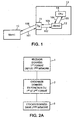
- the figure 1 illustrates an embodiment of the present invention in an architecture comprising a first memory 11 external to a video data processing entity 13.
- This video processing entity comprises a processor, or CPU for 'Central Processing Unit' 14, and a second local memory 12 which is associated with the processor 14.
- This video processing entity 13 further comprises an interface unit 15, or interface device, adapted to, on the one hand, receive 101 from the external memory 11 and transmit 102 to the second memory 12 of the video data, and to, on the other hand, receive 105 from the second memory 12 and transmit 106 to the first memory 11 video data according to an embodiment of the present invention.
- a data transfer 103 can be performed from the second memory 12 to the processor 14 which is in charge of processing the video data stored in the local memory 12.
- the processor 14 after performing a processing step, transfers, in a step 104, the processed data in the second memory 12. This data can then be transmitted to the step 106, at the first memory so as to release memory space in the second memory 12 to allow the processor to continue processing the video data.
- this interface unit symmetrically transfers data from the first memory to the second memory and transfers data from the second memory to the first memory. Therefore, in the following sections, only the transfer of data from the first memory to the second memory is described, since it is easy to deduce the data transfer from the second memory to the first memory.
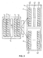
- the figure 2-A illustrates the main steps of a method according to an embodiment of the present invention.
- data is received from a first memory. This data is received per group of data, in each of which they are ordered according to a sequence corresponding to the data storage format in the first memory 11.
- these data are reordered within the data group.
- the new sequence according to which they are arranged is determined as a function of both the first storage format in the first memory and the second format which corresponds to the format adapted for processing the data implemented by the processor 14.
- steps 1-3 can be repeated so as to transfer all the data that is stored in the first memory 11 and which require processing by the processor 14.
- these steps are implemented in the interface unit 15.
- the interface unit 15 can give a read command of the first memory 11 by specifying a memory address corresponding to the first data to be read in said memory as well as a size of the group of data to read, or reading group.
- the interface unit 15 knows the storage format of the data in the first memory and the desired storage format in the second memory for efficient data processing at the processor level and relies on these two formats to determine a function to apply to the group of data received from the first memory 11 before storing these data in the second memory 12. Such a function makes it possible to obtain from the sequence according to which the data are ordered in a first group a sequence according to which the data are ordered in a second group.
- a read group 200 i.e. a first data group retrieved from the first memory 11, is received by the interface unit 15.
- this first group 200 the data is ordered according to a sequence that corresponds in the first format.
- this data group is processed by the interface unit 15 which applies a mathematical function f so as to provide a second data group 202 which comprises the data of the first data group 200, ordered according to a sequence corresponding to the desired storage format in the second memory 12.
- This mathematical function f is determined according to the first and second format.
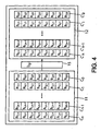
- first case data stored in the first memory in a single common memory space is transferred into two separate memory spaces of the second memory 12.
- data stored in the first memory in a single common memory space are transferred into a single common memory space of the second memory, but with a different storage format.
- each data to be manipulated has a size of 1 byte and is illustrated as a square B i, j .
- the data stored in the memory 11 are grouped in storage cell, each cell C j for j between 0 and n, comprising a number K of data.
- the number K can be equal to 8.
- the data stored in the memory 12 are also grouped in cells C '1 and C j' j 2, respectively in a first and a second buffer memory, for j from 0 to n.
- These storage cells of the second memory 12 may be identical in size to the storage cells of the first memory 11.
- the processor 14 implements a data processing algorithm which requires a separate data processing between two types of data, for example, the chrominance data and the luminance data, whereas in the first memory 11, these two types of data are stored alternately and successively in the order of the sampled pixels of the image in question so that these data are interleaved.
- the interface unit 15 during the transfer of data from the first memory 11 to the second memory 12, formats the data so as to adapt the storage format. data, in the local memory of the processor, the processing to be implemented by the processor 14 on these data.
- the data to be recovered in the first memory are stored in a common memory space of the first memory 11. Then, these data are advantageously distributed in two separate memory spaces, or buffers 21 and 22, of the second memory 12.
- the buffer 21 may contain the luminance data
- buffer 22 may contain the chrominance data.
- the chrominance and luminance data can be stored alternately for the successive pixels of the video images considered, and more precisely for example the luminance data can correspond to the data B i, j where i is an even number, and the chrominance data may correspond to the data B i, j where i is an odd number in the first memory.
- the interface unit 15 can advantageously recover in the first memory all the data B i, j where i is an even number and store these data in the first buffer 21 and recover the data B i, j where i is an odd number and store these data in the second buffer 22.
- the data is retrieved from the memory 11 by reading group 200, each group comprising N data.
- the number N can be equal to 8.
- the reading groups therefore correspond here to the storage cells as defined above.
- each group comprising a number M of data.
- the number M can be equal to the number N.
- the interface unit 15 distributes the data B i, j with i even number in the first buffer 21 and the data B i, j with an odd number in the second buffer 22 to compose respective write groups for the first and second buffers.
- a write group 202 is full, i.e. in this example, whenever a write group contains 8 data to be stored in one of the two buffers, then said write group data is written into the corresponding buffer memory of the second memory 12.
- the interface unit 15 retrieves the data stored in the first memory and applies to them the mathematical function f which is based on both the first storage format of the data in the first memory and the second data storage format in the second memory, which can itself be advantageously defined according to characteristics of the data processing to be applied to these data by the processor 14.
- the cells C j and C j + 1 of the first memory 11, for j an even integer, are distributed in a first cell of the first buffer memory 21 and in a second cell of the second buffer memory 22.
- VS j 1 B 0 , j , B 2 , j , B 4 , j , B 6 , j , B 0 , j + 1 , B 2 , j + 1 , B 4 , j + 1 , B 6 , j + 1
- VS j 2 B 1 , j , B 3 , j , B 5 , j , B 7 , j , B 1 , j + 1 , B 3 , j + 1 , B 5 , j + 1 , B 7 , j + 1 , B 7 , j + 1
- the figure 4 illustrates an embodiment of the present invention corresponding to the second case of transfer.
- the data stored in a first format in a common memory space of the first memory 11 are stored in a second format, but always in a common memory space of the second memory 12.
- An advantageous application of this type of data transfer according to one embodiment of the present invention corresponds to a correction of the order in which the bytes are arranged in memory, or in English 'endianess'.
- a correction takes place in the case where the number N of data included in a reading group 200 is different from the number K of data included in a storage cell of the first memory 11.
- this storage order correction makes it possible to pass from an arrangement of bytes according to which the least significant byte is stored first in the first memory 11, to a byte arrangement according to which the most significant byte is stored first.
- An objective of such an embodiment is therefore to reverse the storage order of the data B i, j within each storage cell C j , between the storage cells of the first memory 11 and the storage cells. of the second memory 12.
- the last data to be transferred in the reading group 200 is the data item B 5, n .
- the fields of the cell C n 'to match the data B 6, n and B 7, n are not filled.
- the present invention covers any type of function that is adapted to transform the first group of data arranged in a first sequence into one or more groups of data arranged in one or more respective sequences.
- the function f has the characteristics required to arrange in the second memory, in an order determined according to characteristics of the algorithm to be applied, the data recovered in the first memory.
- the function f is based on the write mode in the second memory. In the case described, data is written to the second memory in groups of 8 bytes.
- the function f can be adapted to generate a plurality of data groups of 8 bytes.
- this plurality of data groups only a portion of the bytes of the same data group corresponds to one of the bytes of the first data group Z 0 to Z 7 .
- the first data group 200 comprises 8 bytes Z 0 -Z 7 .
- the function f stores these bytes in the second memory as second data groups 202, each comprising one of the bytes of the first data group 200. Then, each of this plurality of second data groups 202 can be written successively in the second memory.
- the function f makes it possible to write at specified locations in the second memory adapted for processing the data by the processor.
- the other bytes of the second data groups 202 may be of any value or may correspond to a byte value which indicates not to write to the second memory, and thus to retain the value stored in the second memory before writing said second byte.
Landscapes
- Engineering & Computer Science (AREA)
- Theoretical Computer Science (AREA)
- Physics & Mathematics (AREA)
- General Engineering & Computer Science (AREA)
- General Physics & Mathematics (AREA)
- Image Processing (AREA)
Claims (9)
- Verfahren zur Verarbeitung von in einem ersten Speicher (11) gespeicherten Daten durch eine Verarbeitungsvorrichtung (13) mit einem Prozessor (14), einem zweiten Speicher (12) und einer Schnittstelleneinrichtung (15), die die Verarbeitungsvorrichtung mit dem ersten Speicher (11) koppelt;
mit den nachfolgenden Schritten, die auf Seiten der Schnittstelleneinrichtung durchgeführt werden, um die Daten zwischen dem ersten Speicher, in dem die Daten gemäß einem ersten Datenformat gespeichert werden, und dem zweiten Speicher, in dem die Daten gemäß einem zweiten Datenformat gespeichert werden, zu übertragen:/a/ Empfangen (1) einer ersten Gruppe von Daten (200), die gemäß einer dem ersten Datenformat entsprechenden Sequenz angeordnet sind, von dem ersten Speicher;/b/ Erhalten zumindest einer zweiten Gruppe von Daten (202) durch Anordnen (2) der Daten der ersten Gruppe gemäß einer neuen Sequenz, die eine Funktion des ersten und des zweiten Datenformats ist;/c/ Speichern (2) der zweiten Gruppe von Daten in dem zweiten Speicher;/d/ Verarbeiten der in dem zweiten Speicher gespeicherten Daten, dann Speichern (104) der verarbeiteten Daten in dem zweiten Speicher gemäß dem zweiten Datenformat;/e/ Empfangen (105) einer Gruppe von verarbeiteten Daten, die gemäß einer dem zweiten Datenformat entsprechenden Sequenz angeordnet sind, von dem zweiten Speicher (12) auf Seiten der Schnittstelleneinrichtung (15);/f/ Erhalten einer weiteren Gruppe von Daten durch Anordnen der verarbeiteten Daten dieser Gruppe gemäß einer neuen Sequenz, die eine Funktion des ersten und des zweiten Datenformats ist; und/g/ Speichern (106) der weiteren Gruppe von Daten in dem ersten Speicher. - Datenverarbeitungsverfahren gemäß Anspruch 1, bei dem der Schritt /b/ durch Anwendung einer bijektiven mathematischen Funktion einer zyklischen Permutation, die eine Funktion des ersten und des zweiten Datenformats ist, auf die erste Gruppe von Daten realisiert wird.
- Datenverarbeitungsverfahren gemäß Anspruch 1, bei dem im Schritt /b/ die Daten der ersten Gruppe von Daten (200) gemäß einer Aufteilung, die eine Funktion des ersten und des zweiten Datenformats ist, jeweils in eine einer Vielzahl von zweiten Gruppen von Daten (202) aufgeteilt werden.
- Datenverarbeitungsverfahren gemäß einem der vorangehenden Ansprüche, bei dem die Auslösung des Schritts /a/ durch ein Lesen der ersten Gruppe von Daten in dem ersten Speicher verursacht wird.
- Datenverarbeitungsverfahren gemäß Anspruch 4, bei dem, wobei das ersten Datenformat für die Speicherung eines ersten und eines zweiten Datentyps auf eine verschachtelte Art und Weise in dem ersten Speicher angepasst ist und das zweite Datenformat zum Speichern des ersten und des zweiten Datentyps in einer unverschachtelten Art und Weise angepasst ist, der Schritt /b/ die nachfolgenden Schritte aufweist:- Gruppieren der Daten des ersten Typs in einer ersten Untergruppe und der Daten des zweiten Typs in einer zweiten Untergruppe; und- Speichern der ersten Untergruppe in einem ersten Teil des zweiten Speichers und Speichern der zweiten Untergruppe in einem zweiten Teil des zweiten Speichers.
- Datenverarbeitungsverfahren gemäß einem der vorangehenden Ansprüche, bei dem die Daten Leuchtdichteinformationen und Farbartinformationen in Bezug auf Bildpunkte eines Videobildes entsprechen.
- Schnittstelleneinrichtung (15) in einer Datenverarbeitungsvorrichtung (13), die zusätzlich einen Prozessor (14) aufweist;
wobei die Schnittstelleneinrichtung zum Übertragen von Daten zwischen einem die Daten gemäß einem ersten Datenformat speichernden ersten Speicher (11) und einem die Daten gemäß einem zweiten Datenformat speichernden zweiten Speicher (12) angepasst ist;
wobei die Schnittstelleneinrichtung aufweist:- eine Empfangseinheit, die angepasst ist zum Empfangen (1) einer ersten Gruppe von Daten (200), die gemäß einer dem ersten Datenformat entsprechenden Sequenz angeordnet sind, von dem ersten Speicher, und die angepasst ist zum Empfangen (105) einer Gruppe von Daten, die durch den Prozessor (14) verarbeitet und gemäß einer dem zweiten Datenformat entsprechenden Sequenz angeordnet sind, von dem zweiten Speicher (12);- eine Formatverwaltungseinheit, die angepasst ist zum Bereitstellen zumindest einer zweiten Gruppe von Daten (202) durch Anordnen (2) der Daten der ersten Gruppe gemäß einer neuen Sequenz, die eine Funktion des ersten und des zweiten Datenformats ist, sowie zum Bereitstellen einer weiteren Gruppe von Daten durch Anordnen der verarbeiteten Daten der Gruppe gemäß einer neuen Sequenz, die eine Funktion des ersten und des zweiten Datenformats ist;- eine Übertragungseinheit, die angepasst ist zum Speichern der zweiten Gruppe von Daten in dem zweiten Speicher und zum Speichern (106) der weiteren Gruppe von Daten in dem ersten Speicher (11). - Schnittstelleneinrichtung gemäß Anspruch 7, bei der die Formatverwaltungseinheit eine bijektive mathematische Funktion einer zyklischen Permutation auf die erste Gruppe von Daten anwendet, wobei die mathematische Funktion eine Funktion des ersten und des zweiten Datenformats ist.
- Datenverarbeitungssystem mit einem Daten gemäß einem ersten Datenformat speichernden ersten Speicher (11) und einer Datenverarbeitungsvorrichtung umfassend einen Daten gemäß einem zweiten Datenformat speichernden zweiten Speicher (12), einen Prozessor (14), der zum Verarbeiten der in dem zweiten Speicher (12) gespeicherten Daten angepasst ist, und eine Schnittstelleneinrichtung (15) gemäß Anspruch 7 oder 8.
Applications Claiming Priority (1)
| Application Number | Priority Date | Filing Date | Title |
|---|---|---|---|
| FR0602695A FR2899354A1 (fr) | 2006-03-28 | 2006-03-28 | Traitement de donnees avec transfert de donnees entre memoires. |
Publications (2)
| Publication Number | Publication Date |
|---|---|
| EP1840751A1 EP1840751A1 (de) | 2007-10-03 |
| EP1840751B1 true EP1840751B1 (de) | 2008-12-17 |
Family
ID=37216098
Family Applications (1)
| Application Number | Title | Priority Date | Filing Date |
|---|---|---|---|
| EP07290370A Not-in-force EP1840751B1 (de) | 2006-03-28 | 2007-03-28 | Datenverarbeitung mit Datenübertragung zwischen Speichern |
Country Status (4)
| Country | Link |
|---|---|
| US (1) | US7769965B2 (de) |
| EP (1) | EP1840751B1 (de) |
| DE (1) | DE602007000362D1 (de) |
| FR (1) | FR2899354A1 (de) |
Families Citing this family (6)
| Publication number | Priority date | Publication date | Assignee | Title |
|---|---|---|---|---|
| US7496695B2 (en) | 2005-09-29 | 2009-02-24 | P.A. Semi, Inc. | Unified DMA |
| US20090248910A1 (en) * | 2008-04-01 | 2009-10-01 | Apple Inc. | Central dma with arbitrary processing functions |
| FR2935056A1 (fr) * | 2008-08-14 | 2010-02-19 | St Microelectronics Rousset | Systeme de traitement de donnees disposant de moyens de traitement repartis pour exploiter des latences intrinseques du systeme |
| US9934244B2 (en) * | 2010-08-13 | 2018-04-03 | At&T Intellectual Property I, L.P. | System and method for file format management |
| US9818170B2 (en) * | 2014-12-10 | 2017-11-14 | Qualcomm Incorporated | Processing unaligned block transfer operations |
| FR3050845B1 (fr) | 2016-04-27 | 2018-04-27 | Bull Sas | Gestion de l'acces a des donnees dans un systeme de stockage |
Family Cites Families (13)
| Publication number | Priority date | Publication date | Assignee | Title |
|---|---|---|---|---|
| US4603320A (en) | 1983-04-13 | 1986-07-29 | Anico Research, Ltd. Inc. | Connector interface |
| US4972470A (en) | 1987-08-06 | 1990-11-20 | Steven Farago | Programmable connector |
| TW226047B (de) * | 1990-03-27 | 1994-07-01 | Ibm | |
| US6480913B1 (en) * | 1998-07-17 | 2002-11-12 | 3Dlabs Inc. Led. | Data sequencer with MUX select input for converting input data stream and to specific output data stream using two exclusive-or logic gates and counter |
| JP2000305891A (ja) * | 1999-04-22 | 2000-11-02 | Canon Inc | Dmaコントローラおよびdma制御方法 |
| EP1058193A1 (de) * | 1999-05-31 | 2000-12-06 | Deutsche Thomson-Brandt Gmbh | Verfahren und Datenverarbeitungseinheit zur Vorverarbeitung von Datenpaketen in einer Datenbusschnittstelleneinheit |
| US20020162119A1 (en) * | 2000-07-10 | 2002-10-31 | Ariel Yagil | Upstream hi-phy lite system |
| US20020111972A1 (en) * | 2000-12-15 | 2002-08-15 | Virtual Access Networks. Inc. | Virtual access |
| JPWO2002060175A1 (ja) * | 2001-01-25 | 2004-05-27 | ソニー株式会社 | データ転送装置 |
| EP1585128A4 (de) * | 2002-11-20 | 2008-05-07 | Matsushita Electric Industrial Co Ltd | Integrierte videodaten dateiintegrationseinrichtung undverfahren und integrierte videodatendateiwiedergabeeinrichtung und verfahren |
| KR20050058939A (ko) * | 2003-12-13 | 2005-06-17 | 삼성전자주식회사 | 광디스크의 파일 시스템 포맷의 변환 방법 및 그 장치 |
| US7599611B2 (en) * | 2004-09-13 | 2009-10-06 | Lg Electronics Co. | Recording medium, and method and apparatus of reproducing data recorded on the same |
| JP4740583B2 (ja) * | 2004-12-13 | 2011-08-03 | ヤマハ株式会社 | 音楽データ処理装置及びプログラム |
-
2006
- 2006-03-28 FR FR0602695A patent/FR2899354A1/fr active Pending
-
2007
- 2007-03-27 US US11/729,308 patent/US7769965B2/en active Active
- 2007-03-28 DE DE602007000362T patent/DE602007000362D1/de active Active
- 2007-03-28 EP EP07290370A patent/EP1840751B1/de not_active Not-in-force
Also Published As
| Publication number | Publication date |
|---|---|
| EP1840751A1 (de) | 2007-10-03 |
| US20070288691A1 (en) | 2007-12-13 |
| DE602007000362D1 (de) | 2009-01-29 |
| FR2899354A1 (fr) | 2007-10-05 |
| US7769965B2 (en) | 2010-08-03 |
Similar Documents
| Publication | Publication Date | Title |
|---|---|---|
| EP0618722B1 (de) | Verfahren und Einrichtung zur Dekodierung von komprimierten Bildern | |
| EP1840751A1 (de) | Datenverarbeitung mit Datenübertragung zwischen Speichern | |
| EP0206847A1 (de) | Rechnungseinrichtungen von Cosinustransformationen, solche Rechnungseinrichtungen enthaltende Kodierungs- und Dekodierungseinrichtung von Bildern | |
| WO2010037570A1 (fr) | Dispositif de traitement en parallele d'un flux de donnees | |
| FR2834104A1 (fr) | Procede de transmission d'objets entre un serveur et un terminal client mettant en oeuvre une gestion de cache, systeme de transmission, serveur et terminal correspondants | |
| EP0920157A1 (de) | Verwaltungseinrichtung eines gemeinsamen Pufferspeichers | |
| EP0440301B1 (de) | Abspeicherungsverfahren für die Bildverarbeitung und Gerät,um dieses einzusetzen | |
| FR2618282A1 (fr) | Procedes et appareils d'emmagasinage de signaux video numeriques. | |
| EP0716395B1 (de) | Verfahren zum Dekodieren komprimierter Bilder | |
| FR2780186A1 (fr) | Procede et dispositif de decodage d'une image, comprimee notamment selon les normes mpeg, en particulier une image bidirectionnelle | |
| EP3386191B1 (de) | Array-sensor mit zeitkodierung ohne arbitrierung | |
| FR2780184A1 (fr) | Procede et dispositif de decodage d'images, permettant un nombre reduit d'ouvertures de pages-memoire dans le traitement de prediction | |
| EP1161035B1 (de) | Verfahren zur wechselseitigen Übertragung von Steuerungsparametern durch ein Kommunikationsnetz | |
| EP1286550A2 (de) | Vorrichtung zur Verarbeitung und Leiten von Daten | |
| EP4206938B1 (de) | System zur direkten datenübertragung | |
| EP0792071B1 (de) | MPEG2-Dekodierer | |
| EP4109451B1 (de) | Speicherschaltkreis für sparse-daten | |
| EP2553655B1 (de) | Architektur zur datenstromverarbeitung mit funktion zur erweiterung der nachbarmaske | |
| FR2774242A1 (fr) | Systeme et procede de commutation asynchrone de cellules composites, et modules de port d'entree et de port de sortie correspondants | |
| FR3031822A1 (fr) | Telechargement de donnees sur un equipement distant | |
| EP1032125A1 (de) | Empfänger, programmierbare Schaltungsanordnung und Verfahren zur Berechnung von digitalen Filtern | |
| EP1971152A2 (de) | Datenverwaltung für eine Bildverarbeitung | |
| FR2825167A1 (fr) | Procede et systeme d'acces a une memoire commune | |
| EP1355454B1 (de) | Routinggerät mit paralleler Verarbeitung | |
| EP0674444A1 (de) | Filter für Matrix von Pixeln |
Legal Events
| Date | Code | Title | Description |
|---|---|---|---|
| PUAI | Public reference made under article 153(3) epc to a published international application that has entered the european phase |
Free format text: ORIGINAL CODE: 0009012 |
|
| AK | Designated contracting states |
Kind code of ref document: A1 Designated state(s): AT BE BG CH CY CZ DE DK EE ES FI FR GB GR HU IE IS IT LI LT LU LV MC MT NL PL PT RO SE SI SK TR |
|
| AX | Request for extension of the european patent |
Extension state: AL BA HR MK YU |
|
| 17P | Request for examination filed |
Effective date: 20080328 |
|
| AKX | Designation fees paid |
Designated state(s): DE FR GB IT |
|
| GRAP | Despatch of communication of intention to grant a patent |
Free format text: ORIGINAL CODE: EPIDOSNIGR1 |
|
| GRAS | Grant fee paid |
Free format text: ORIGINAL CODE: EPIDOSNIGR3 |
|
| GRAA | (expected) grant |
Free format text: ORIGINAL CODE: 0009210 |
|
| AK | Designated contracting states |
Kind code of ref document: B1 Designated state(s): DE FR GB IT |
|
| REG | Reference to a national code |
Ref country code: GB Ref legal event code: FG4D Free format text: NOT ENGLISH |
|
| REF | Corresponds to: |
Ref document number: 602007000362 Country of ref document: DE Date of ref document: 20090129 Kind code of ref document: P |
|
| PLBE | No opposition filed within time limit |
Free format text: ORIGINAL CODE: 0009261 |
|
| STAA | Information on the status of an ep patent application or granted ep patent |
Free format text: STATUS: NO OPPOSITION FILED WITHIN TIME LIMIT |
|
| 26N | No opposition filed |
Effective date: 20090918 |
|
| REG | Reference to a national code |
Ref country code: FR Ref legal event code: ST Effective date: 20091130 |
|
| PG25 | Lapsed in a contracting state [announced via postgrant information from national office to epo] |
Ref country code: FR Free format text: LAPSE BECAUSE OF NON-PAYMENT OF DUE FEES Effective date: 20091123 |
|
| PG25 | Lapsed in a contracting state [announced via postgrant information from national office to epo] |
Ref country code: IT Free format text: LAPSE BECAUSE OF FAILURE TO SUBMIT A TRANSLATION OF THE DESCRIPTION OR TO PAY THE FEE WITHIN THE PRESCRIBED TIME-LIMIT Effective date: 20081217 |
|
| GBPC | Gb: european patent ceased through non-payment of renewal fee |
Effective date: 20110328 |
|
| PG25 | Lapsed in a contracting state [announced via postgrant information from national office to epo] |
Ref country code: GB Free format text: LAPSE BECAUSE OF NON-PAYMENT OF DUE FEES Effective date: 20110328 |
|
| PGFP | Annual fee paid to national office [announced via postgrant information from national office to epo] |
Ref country code: DE Payment date: 20120223 Year of fee payment: 6 |
|
| REG | Reference to a national code |
Ref country code: DE Ref legal event code: R119 Ref document number: 602007000362 Country of ref document: DE Effective date: 20131001 |
|
| PG25 | Lapsed in a contracting state [announced via postgrant information from national office to epo] |
Ref country code: DE Free format text: LAPSE BECAUSE OF NON-PAYMENT OF DUE FEES Effective date: 20131001 |