EP1839166B1 - Schaltmatrixarchitektur eines gemeinsamen speichers - Google Patents
Schaltmatrixarchitektur eines gemeinsamen speichers Download PDFInfo
- Publication number
- EP1839166B1 EP1839166B1 EP06717512A EP06717512A EP1839166B1 EP 1839166 B1 EP1839166 B1 EP 1839166B1 EP 06717512 A EP06717512 A EP 06717512A EP 06717512 A EP06717512 A EP 06717512A EP 1839166 B1 EP1839166 B1 EP 1839166B1
- Authority
- EP
- European Patent Office
- Prior art keywords
- shared memory
- circuitry
- memory
- transmit
- receive
- Prior art date
- Legal status (The legal status is an assumption and is not a legal conclusion. Google has not performed a legal analysis and makes no representation as to the accuracy of the status listed.)
- Expired - Lifetime
Links
Images

Classifications
-
- G—PHYSICS
- G11—INFORMATION STORAGE
- G11C—STATIC STORES
- G11C7/00—Arrangements for writing information into, or reading information out from, a digital store
- G11C7/10—Input/output [I/O] data interface arrangements, e.g. I/O data control circuits, I/O data buffers
- G11C7/1048—Data bus control circuits, e.g. precharging, presetting, equalising
-
- G—PHYSICS
- G11—INFORMATION STORAGE
- G11C—STATIC STORES
- G11C7/00—Arrangements for writing information into, or reading information out from, a digital store
- G11C7/10—Input/output [I/O] data interface arrangements, e.g. I/O data control circuits, I/O data buffers
- G11C7/1075—Input/output [I/O] data interface arrangements, e.g. I/O data control circuits, I/O data buffers for multiport memories each having random access ports and serial ports, e.g. video RAM
-
- H—ELECTRICITY
- H04—ELECTRIC COMMUNICATION TECHNIQUE
- H04L—TRANSMISSION OF DIGITAL INFORMATION, e.g. TELEGRAPHIC COMMUNICATION
- H04L49/00—Packet switching elements
- H04L49/10—Packet switching elements characterised by the switching fabric construction
- H04L49/103—Packet switching elements characterised by the switching fabric construction using a shared central buffer; using a shared memory
-
- H—ELECTRICITY
- H04—ELECTRIC COMMUNICATION TECHNIQUE
- H04L—TRANSMISSION OF DIGITAL INFORMATION, e.g. TELEGRAPHIC COMMUNICATION
- H04L49/00—Packet switching elements
- H04L49/10—Packet switching elements characterised by the switching fabric construction
- H04L49/101—Packet switching elements characterised by the switching fabric construction using crossbar or matrix
-
- H—ELECTRICITY
- H04—ELECTRIC COMMUNICATION TECHNIQUE
- H04L—TRANSMISSION OF DIGITAL INFORMATION, e.g. TELEGRAPHIC COMMUNICATION
- H04L49/00—Packet switching elements
- H04L49/35—Switches specially adapted for specific applications
- H04L49/351—Switches specially adapted for specific applications for local area network [LAN], e.g. Ethernet switches
Definitions
- the present invention relates to a switch fabric architecture. More specifically, the present invention provides a shared memory switch architecture which may be employed to switch frames or packets of arbitrary lengths between any of its ports with sustained high speed throughputs.
- Shared memory architectures are advantageous for high speed switches with many ports because they make more efficient use of memory. That is, if the memory resides in the ports themselves, the memory in idle ports sits unused while the memory in active ports may be overworked, particularly where the transmission protocol allows very large packets.
- the transmission protocol for which the switch is designed has multicast requirements (e.g., Ethernet)
- shared memory only requires that that a multicast packet be written to memory once. The multiple ports for which the multicast packet is intended then read the same memory location, an operation which requires no more overhead than if the ports were reading different memory locations. Because of this suitability, shared memory architectures are particularly popular for implementing Ethernet switches.
- US-2003/0088694 discloses a multicasting method and switch for the scheduling of multicast frames in a switching network.
- a destination identifier in an incoming frame to be multicast is used to determine an output port mask via a table lookup.
- the output port mask is used to determine which selected output ports receive a copy of the incoming frame.
- the selected ports are copied concurrently.
- WO-03/043272 discloses a method of buffering packets in a packet switching network.
- the method comprises receiving a packet from a network, splitting the packets into a number of packet data units (PDU's), stripping at least some of the PDU's over a plurality of memory banks, retrieving the PDU's from the memory banks, and storing the retrieved PDU's in the sequence they are to be transmitted.
- PDU's packet data units
- a shared memory architecture which enables a high port count despite a modest maximum memory speed.
- a shared memory having a plurality of receive ports and a plurality of transmit ports characterized by a first data rate.
- a memory includes a plurality of memory banks organized in rows and columns. Operation of the memory array is characterized by a second data rate.
- Non-blocking receive crossbar circuitry is operable to connect any of the receive ports with any of the memory banks.
- Non-blocking transmit crossbar circuitry is operable to connect any of the memory banks with any of the transmit ports.
- Buffering is operable to decouple operation of the receive and transmit ports at the first data rate from operation of the memory array at the second data rate.
- Scheduling circuitry is operable to control interaction of the ports, crossbar circuitry, and memory array to effect storage and retrieval of the data segments in the shared memory.
- the scheduling circuitry is further operable to facilitate striping of each data segment of a frame across the memory banks in one of the rows, and to facilitate striping of successive data segments of the frame across successive rows in the array.
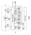
- Fig. 1 is a block diagram illustrating a multi-ported switch according to a specific embodiment of the invention.
- Fig. 2 is a block diagram illustrating portions of a datapath for use with specific embodiments of the invention.
- Fig. 3 is a block diagram illustrating portions of a datapath for use with specific embodiments of the invention.
- Fig. 4 is a more detailed block diagram illustrating portions of a datapath for use with specific embodiments of the invention.
- Figs 5A and 5B are block diagrams illustrating distribution of control in a datapath for use with specific embodiments of the invention.
- Fig. 6 is a more detailed block diagram illustrating distribution of control in a datapath for use with specific embodiments of the invention.
- Fig. 7 is a block diagram illustrating the receive portion of a port for a multi-ported switch according to a specific embodiment of the invention.
- Fig. 8 is a block diagram illustrating the transmit portion of a port for a multi-ported switch according to a specific embodiment of the invention.
- Fig. 9 is a block diagram illustrating operation of a scheduler according to a specific embodiment of the invention.
- Asynchronous VLSI is an active area of research and development in digital circuit design. It refers to all forms of digital circuit design in which there is no global clock synchronization signal.
- Delay-insensitive asynchronous designs by their very nature are insensitive to the signal propagation delays which have become the single greatest obstacle to the advancement of traditional design paradigms. That is, delay-insensitive circuit design maintains the property that any transition in the digital circuit could have an unbounded delay and the circuit will still behave correctly.
- the circuits enforce sequencing but not absolute timing. This design style avoids design and verification difficulties that arise from timing assumptions, glitches, or race conditions.
- asynchronous processes and circuits described herein may be represented (without limitation) in software (object code or machine code), in varying stages of compilation, as one or more netlists, in a simulation language, in a hardware description language, by a set of semiconductor processing masks, and as partially or completely realized semiconductor devices.
- software object code or machine code
- netlists netlists
- simulation language simulation language
- hardware description language hardware description language
- the various types of computer-readable media e.g., Verilog, VHDL
- simulatable representations e.g., SPICE netlist
- semiconductor processes e.g., CMOS, GaAs, SiGe, etc.
- device types e.g., FPGAs
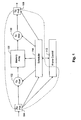
- a receive (Rx) crossbar 102 switches incoming data from any of a plurality of Rx ports 104 to any of a plurality of banks of memory in memory array 106.
- the data in memory array 106 are switched to any of a plurality of transmit (Tx) ports 108 via Tx crossbar 110.
- Tx transmit
- each Rx port 104 and a corresponding one of Tx ports 108 correspond to an Ethernet port. It will be understood that only single Rx and Tx ports are shown for the sake of simplicity.
- embodiments of the invention are discussed below with reference to specific numbers of ports, e.g., 20, 24, 32, etc. It will be understood, however, that these numbers are merely exemplary and should not be used to limit the scope of the invention.
- Frame control 112 When data are received by an Rx port 104, a portion of the data, e.g., a frame or packet header, is copied and sent to frame control block 112, and all of the data, i.e., including the copied portion and the payload, are sent to memory array 106 for storage.
- Frame control 112 is a pipelined unit which provides frame control information to scheduler 114 to facilitate storage of the payload in memory. Frame control 112 makes decisions on a per frame basis including, for example, whether to modify the frame, or whether to discard it. Frame control 112 then sends its decision to scheduler 114 which is responsible for generating the controls which move and store the data.
- crossbars 102 and 110, memory array 106, scheduler 114, a portion of each of ports 104 and 108, and a portion of frame control 112 are implemented according to the asynchronous design style mentioned above.
- the remaining portions of the ports and the frame control are implemented using any of a variety of conventional synchronous design techniques.
- the synchronous portions of the ports present the expected external interfaces expected by the system(s) to which the switch is connected.
- the synchronous portion of the frame control is implemented according to a synchronous design style, e.g., Verilog, at least in part because it comprises complex but relatively straightforward logic for which such design styles are well suited. The details and advantages of this approach will become more apparent with reference to the discussion below.
- the interfaces between synchronous and asynchronous portions of the architecture may be implemented according to the techniques described in U.S. Patent Publication No. 20030159078 for Techniques For Facilitating Conversion Between Asynchronous and Synchronous Domains published on August 21, 2003 (Attorney Docket No. FULCP002).
- the switch architecture of the present invention is operable to switch frames or packets of arbitrary length between its ports.
- memory in the array is allocated in fixed-size blocks referred to herein as “segments.”
- data are moved through the switch fabric in smaller fixed-size blocks referred to herein as “subsegments.”
- Rx crossbar 202 is shown as an N channel x 64 channel crossbar
- Tx crossbar 204 is shown as a 64 x N crossbar.
- N may take on any of a wide range of values.
- the specific architecture described is physically configured to handle up to 32 ports. However, much of the performance discussion assumes that the architecture is provisioned for some number less than 32 ports, e.g., 20 or 24. It should be understood that N may also take on values greater than 32, although ultimately, N is limited by and scales with the speed of the memory for which the design is to be fully provisioned.
- each channel comprises a multi-bit data path, e.g., a 32-bit data path.
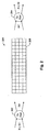
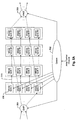
- Memory array 206 may be thought of as an array of 4,096 segments of 256 bytes each, each segment corresponding to four sub-segments of 64 bytes each.
- the array is divided into 64 16kB banks 208 of SRAM, one bank for each of the 64 Rx and Tx crossbar channels, i.e., the write channel for each bank being connected to one of the Rx crossbar output channels, and the read channel being connected to one of the Tx crossbar input channels.
- the exemplary array of Fig. 2 is shown having 16 columns and 4 rows, it will be understood that the numbers of columns and rows may vary significantly for the myriad applications to which the invention is suited.
- each 4-byte word of the sub-segment is placed in incrementing SRAM locations, "striping" through the 64 SRAM banks in a linked list of segments corresponding to the frame.
- each subsegment is striped through the banks in a particular row, with successive sub-segments in a segment being striped in successive rows.
- successive frames starting in a given bank are written beginning at the same subsegment. However, this results in the "lower" portions of the memory banks being worked very hard while the "upper” portions are frequently idle. Therefore, according to some embodiments, different subsegment starting points within the bank are selected for successive frames starting in a particular bank. This selection may be done pseudo-randomly or deterministically. According to one embodiment, the selection of the starting point for a new frame is responsive to detection of the condition where multiple ports are trying to access a particular bank of memory at the same time. Such an approach may be used to reduce the likelihood that frames will be dropped for embodiments in which the SRAM array operates more slowly for a given number of ports than the maximum packet rate. Alternatively, such an approach may be used to provide additional margin.
- embodiments of the invention are contemplated in which the sub-segments within a segment are rotated. Selection may again be done pseudo-randomly or deterministically. Deterministic selection might, for example, employ a linear order. Alternatively, a "score-boarding" approach might be employed in which selection is based on a least-recently-allocated approach.
- each port must be able to handle 15 million frames ( ⁇ 64 bytes) per second with fixed-size 20 byte gaps between successive frames (i.e., 10 Gigabit data rate).
- the asynchronous SRAM can stall during the 20-byte gaps between frames, only the crossbars need to be running fast enough to keep up with the burst speed, while the memory can be running at the sustained speed, i.e., the frame rate times the number of ports (which is roughly equivalent to 360 MHz for a dual-ported SRAM, or 720 MHz for a single-ported SRAM), without dropping frames.
- the maximum data rate is handled by the manner in which the data are striped through the SRAM. That is, if 24 ports are assumed, a single SRAM row is going to receive, at most, twenty-four 64 byte subsegments before one of two things happens. If the frame being received on a given port is complete, the SRAM bank will go idle. If, on the other hand, any of the 24 frames has additional subsegments, the data will shift to the next row of SRAM banks, (which has been sitting idle and ready to go) and continue striping through the SRAM. Thus, because of the inter-frame gaps, the asynchronous SRAM never has to operate faster than the maximum frame rate (as opposed to the maximum data rate) to be fully provisioned.
- asynchronous data path takes advantage of this slack in the system to smooth out the burstiness of the incoming data, making a 24-port switch efficient.
- a comparable dual-ported synchronous memory operating at 360 MHz could only support 18 ports.
- embodiments of the present invention may be implemented using a single-ported asynchronous SRAM architecture (which alternates reads and writes) described in U.S. Patent Application No. 10/890,816 for ASYNCHRONOUS STATIC RANDOM ACCESS MEMORY filed July 13, 2004 (Attorney Docket No. FULCP008).
- such a memory can operate at the equivalent 720 MHz rate required by 24 ports, and yet have the relatively small footprint of a single-ported architecture.
- a comparable synchronous system would have to resort to the use of a dual-ported architecture (which consumes considerably more area), because single-ported designs for a 24-port switch would have to operate at 938 MHz, considered too high of a frequency for standard synchronous memory implementations in 0.13um Technology.
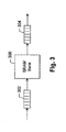
- burst FIFOs 302 and 304 are provided between each memory bank 306 and the corresponding Rx crossbar output channel and Tx crossbar input channel.
- FIFOs 302 and 304 are sufficiently large to handle the worst case bursts from the crossbar channels. That is, the Rx and Tx crossbars are provisioned to receive and transmit data from and to a large number of ports (e.g., 20 or more). This imposes an operation speed requirement on the crossbars which is difficult to achieve for SRAM bank 306.
- FIFOs 302 and 304 allow for SRAM bank 306 to have a more modest operation speed while also allowing the Rx and Tx crossbars to receive and transmit data in bursts at their respective maximum operation speeds.
- the Rx and Tx crossbars may each be implemented as a single 32 x 64 or 64 x 32 crossbar, respectively.
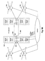
- the 32 ports are connected to 64 banks of memory using two 16 x 16 crossbars (402-408) for both the receive and transmit sides of the ports in combination with 16 2 x 4 crossbars 410 and 16 4 x 2 crossbars 412 to get in and out of the individual memory banks 414. That is, for example, each 32-bit output channel of crossbar 402 is coupled to one of the two input channels of one of crossbars 410.
- Each of the four output channels of each crossbar 410 is coupled to the write channel of one of the four associated memory banks 414.
- the read channel of each of memory banks 414 is coupled to one of the four input channels of the associated one of crossbars 412.
- Each of the output channels of each crossbar 412 is then coupled to one of the input channels of one of the crossbars 406 or 408.
- This distributed, non-blocking crossbar system connects each of the ports (up to 32) to the read and write channels of each of the 64 banks of SRAM.
- a Clos architecture has two requirements, i.e., 1) a CCB (constant cross-sectional bandwidth) (2N-1 links through a mid tier of switches); and 2) some mechanism for scheduling onto the available links.
- CCB constant cross-sectional bandwidth
- striping techniques create a non-blocking means of scheduling the segments onto the memory elements. This enables scaling up the port count to the fundamental limit of the memory speed without introducing any blocking.
- non-blocking architectures please refer to A study of non-blocking switching networks by Charles Clos, The Bell System Technical Journal, 1953, vol. 32, no. 2, pages 406-424 .
- each individual crossbar may be implemented in a variety of ways. According to one set of embodiments, the crossbars may be implemented as described in U.S. Patent Publication No. 20030146073 A1 for Asynchronous Crossbar With Deterministic or Arbitrated Control published on August 7, 2003 (Attorney Docket No. FULCP001).
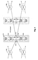
- Figs. 5A , 5B and 6 Distribution of control signals to the datapath described above will now be discussed with reference to Figs. 5A , 5B and 6 .
- the Rx and Tx crossbars are once again represented as single 32 x 64 and 64 x 32 crossbars for simplicity.
- Both Figs. 5A and 5B show the control as a single block also for simplicity. Additional details regarding how the control signals are generated is discussed below with reference to subsequent figures.
- control 502 receives a single control stream (represented as the "array control channel" input to control 502) from a scheduler (not shown) and generates control channels for Rx crossbar 504, SRAM banks 506, and Tx crossbar 508.
- the SRAM control information includes an address and a read/write bit.
- the crossbar control information for each crossbar identifies the crossbar input and output channels (i.e., the from/to crossbar port combination) and the length of the frame or packet.
- the array control channel includes a read bit, a read address, a read port, a read length, a write bit, a write address, a write port, and a write length.
- the read and write lengths represent how many unused words in the final 64 byte subsegment of a frame. This enables reading and writing to stop when a frame ends rather than taking up memory locations with dummy information.
- the array control channel therefore, simultaneously provides information for writing a 64 byte subsegment to memory and reading a 64 byte subsegment from memory, wherein the two subsegments may or may not be related.
- the read and write channels may be fully provisioned if each operates at about 600 MHz.
- this translates to an equivalent data rate of operation for control 502 of 1.2 GHz.
- the actual data rate is just 600 MHz.
- a lower max pipeline speed, or a higher port count could be achieved by breaking up the control stream into 4 independent streams which follow each of the four crossbars (note: this assumes the 4 crossbar example).
- Control 502 translates one command on the array control channel to everything that is needed to write one 64-byte subsegment to the SRAM array and read one 64-byte subsegment from the array.
- the manner in which the control information is transmitted to the crossbars and the SRAM array makes it possible to begin executing the next command after only the first word(s) of the previous command has been written/read. For example, on the receive side, word 0 associated with one command is transmitted to memory on the cycle following word 0 of the previous command (or simultaneously with word 1 of the previous command). That is, successive commands are executed out-of-sync by one cycle.
- control information is introduced into the SRAM array. That is, the control information is provided to the first “column” of SRAM banks 506 and then “rippled” across the array to the corresponding banks in the other columns as indicated by arrows 510. Because of the manner in which frames are "striped” across the SRAM banks, the same start address is used in each successive bank to store the subsegments of a particular frame. Therefore, the address information need only be sent from control 502 one time, and then shared among the columns.
- the length is decremented so that the write or read stops when there are no more data to be stored or read, i.e., the address information ripples until the length of the subsegment (16 words or less) is reached and then "dies out.” This enables efficient variable length transfer without the use of a tail bit in the datapath.
- the Rx and Tx crossbars are pipelined and fully parallel so that they can start transmitting a subsegment (which can take up to 16 cycles) every cycle.
- Each of the output channels of two 16 x 16 Rx crossbars 552 and 554 is connected to an input channel of a 2 x 4 crossbar 556 in each of 16 columns of SRAM banks 558.
- Each of the four output channels of each crossbar 556 is connected to one of the four SRAM banks 558. In this way, up to 32 Rx input channels may be connected to each of the 64 banks of SRAM.
- each of the SRAM banks in a column is connected to the input channels of the column's 4 x 2 crossbar 560.
- the two output channels of each crossbar 560 are connected to one input channel of Tx crossbars 562 and 564, respectively. In this way, each of the 64 SRAM banks may be connected to up to 32 Tx output channels.
- Control channels are sent by control 502 to the crossbars in the datapath.
- One control channel is sent for each of crossbars 552, 554, 562 and 564.
- One control channel is also sent to crossbars 556 and 560 in the first "column” of SRAM banks. This control information is then rippled across the other 16 "columns" (as indicated by arrows 566) such that successive words of the frame are stored in, i.e., striped across, successive SRAM banks as described above for the SRAM control information.
- the control information for each 16 x 16 crossbar includes 8 bits; 4 bits identifying the input or output channel (depending on whether it is Rx or Tx) and 4 bits indicating the "length," i.e., the number of words in the subsegment.
- the control information for the 2 x 4 and 4 x 2 crossbars includes 7 bits; 3 bits to encode the input/output channel combination, and 4 bits for the subsegment length.
- the control information to each of the four SRAM banks 558 in the first "column" of the SRAM array includes 17 bits, a 12-bit address (i.e., one of 4096 possible 256 byte segments in each bank), one read/write bit, and 4 bits for subsegment length. As described above, this information is then rippled across the array to the corresponding banks in each successive columns (i.e., until the information "dies out.”).
- Fig. 6 illustrates how a single stream of 4 bits of input channel information and 4 bits of length information may be distributed throughout one of the 16 x 16 Rx crossbars sufficiently quickly to keep up with the required data rate.
- a similar but "mirror image" control path is implemented for the 16 x 16 Tx crossbars.
- the 8 bits of information is copied (602) with one stream being used for serial "outer” control information and the other for parallel “inner” control information. That is, as will be described, the control for the outer crossbar channels (i.e., input side for Rx and output side for Tx) is serialized, while the control for the inner crossbar channels (i.e., input side for the Tx and output side for the Rx) is parallelized.
- the outer control information is split 16 ways (604), i.e., one for each input port, according to the 4 bits of input channel information. This serializes the control to the input channels of the Rx crossbars while also allowing the control information for successive subsegments to be distributed on successive cycles even though subsegments may take up to 16 cycles to transmit.
- the control is repeated (606) to the corresponding input channel of the crossbar until the length of the subsegment is reached (as determined by decrementing the length count).
- the inner control information is rippled through the output channel control of the Rx crossbar (608-0 through 608-15), successively connecting the designated input channel of the Rx crossbar to as many of the 16 output channels as are required to transmit the subsegment to the successive banks of the SRAM array (as indicated by the 4-bit length).
- the control of the Rx crossbar output channels is parallelized.
- the control for the 16 x 16 Tx crossbars is nearly identical except that it is the control for the input channels of the Tx crossbars which is parallelized and the control for output channels which is serialized.
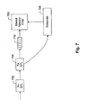
- Fig. 7 shows a simplified block diagram of the Rx portion of a port including Rx Ethernet port logic (EPL) 702, a synchronous block which presents the expected interface characteristics (as defined in the Ethernet specification) to the outside of the switch.
- Rx asynchronous port logic (APL) 704 is, as the name implies, an asynchronous block which provides the appropriate portion of the incoming data from Rx EPL 702 to scheduler 706 (operation of which is described below) and the frame control (not shown).
- Rx APL 704 For every subsegment to be stored in the SRAM array 708, Rx APL 704 provides 8 bits of subsegment data (RxSS) to scheduler 706, 6 bits encoding the length of the subsegment (i.e., 1-64 bytes), an end-of-frame (EOF) bit, and an error bit. The subsegment data are placed in FIFO 710 and are then stored in array 708 in accordance with the control information from scheduler 706. Rx APL 704 also provides the first 16 bytes of every frame and the length and error flags (from the end of the frame) to the frame control (not shown) for use as will be described below.
- RxSS subsegment data
- EDF end-of-frame
- FIFO 710 is a "jitter" FIFO which has a couple of benefits. Because the crossbar(s) of the present invention are non-blocking, data do not back up into the switch port logic (e.g., Rx EPL 702). However, there may be a small wait time until arbitration permission is received. FIFO 710 provides buffering to absorb this latency. In addition, FIFO 710 allows data to be streamed into the shared memory array at the speed of the crossbar(s) rather than at the speed of the port logic, i.e., it decouples the operating speeds of the port logic and the crossbars. According to a specific embodiment, FIFO 710 (which may be integrated with Rx APL 704) can store an entire segment, thereby enabling cut-through operation of the shared memory.
- Rx APL 704 can store an entire segment, thereby enabling cut-through operation of the shared memory.
- Rx APL 704 happens to be asynchronous in this particular embodiment. Rather, it should be conceptualized as the boundary of a generic switch element designed according to the present invention which includes features such as variable packet storage, cut-through forwarding, fully provisioned multicast, and egress tagging.
- Rx EPL 702 merely gives an application specific context (i.e., Ethernet), a "protocol personality" according to which such a switch may be implemented.
- Interconnect technologies e.g., Serial Rapid I/O, Advanced Switching, Infiniband, etc.
- Serial Rapid I/O e.g., Serial Rapid I/O
- Advanced Switching e.g., Advanced Switching
- Infiniband e.g., Infiniband
- Multiple personalities of a particular interconnect technology e.g., multiple Ethernet personalities
- higher level processing e.g., IP processing
- Fig. 8 shows a simplified block diagram of the Tx portion of a port.
- Tx APL 802 tracks the state of FIFO 804 and sends a "ready" signal to scheduler 806 when there is room in FIFO 804 for another subsegment from SRAM array 808.
- Scheduler 806 provides 8 bits of subsegment data (TxSS) to counter 810, 6 bits for the length of the packet, an EOF bit, and an error bit.
- TxSS subsegment data
- Tx APL 802 does not start draining subsegments from FIFO 804 until there are sufficient subsegments for the current frame in the FIFO to ensure that it doesn't "run dry.” This is ensured using counter 810 which asserts a "go" signal to Tx APL 802 only after one of two conditions is satisfied; either when counter 810 completes its count or when the end-of-frame is detected.
- counter 810 is reset for each frame using a programmable value received from scheduler 806.
- a register in the scheduler was chosen for architectural convenience. It will be understood that this value may be stored in a register anywhere in the system. According to various specific implementations, the counter value may take any one of a plurality of values depending on current or expected system conditions.
- programmable values there are three different programmable values used which correspond to three different conditions.
- the counter value is zero, i.e., the "go" signal is asserted and Tx APL 802 is immediately allowed to start draining FIFO 804 (i.e., the frame is less than or equal to one subsegment and there is no jitter by definition).
- the counter value is set such that the "go" signal is asserted when some number of subsegments (e.g., four) are in the FIFO (e.g., the writing of the frame is one segment (256 bytes) ahead of the reading).
- the counter value is set such to twice the value for the store-and-forward case as this case experiences the most jitter.
- Counter 810 also receives notification of the end-of-frame from EOF detector 812 which receives a copy of the subsegment data and asserts the EOF signal to counter 810 when the end-of-frame is detected. In response to the EOF signal, counter 810 asserts the "go" signal to Tx APL 802 (unless it has already been asserted based on the counter value).
- the frame control also sends frame level information (i.e., egress tag packet processing) to Tx APL 802 (or EPL 816) for modifying the frame on its way out of the switch.
- This frame level information (which may pass through scheduler 806) is sideband information required to transmit a frame and typically commands the Tx APL or EPL to modify the frame header in some way.
- this frame level information could include VLAN tag modification information.
- the RxSS error bit indicates an error, if the error can catch up to the frame before it begins transmission, i.e., the switch "knows" about the error before transmission begins, then the frame is silently discarded. This will always happen in store-and-forward mode. However, in cut-through mode, this will only happen under some circumstances, e.g., switch congestion or short frames. If the TxSS error bit indicates an error, a corrupted CRC is inserted in the frame (e.g., in the EPL).
- jitter refers to any delay between successive operations which is introduced by any of the arbitration, serialization, and banking in the switch element of the present invention.
- a first source of jitter is due to the fact that the scheduler queries each port in sequence, but the interval between consecutive queries of the same port can vary dramatically, e.g., 0-35 ns.
- a second and larger source of jitter is due to the fact that there is a fair amount of control channel buffering in the system to smooth out the "burstiness" of the datapath performance. That is, although this buffering has the positive effect of smoothing out the system performance relative to such bursts, it is possible that this slack, when full, may introduce jitter into the system.
- control information e.g., headers
- the data in the array do not need to have additional parity bits because the frames already include a CRC.
- the control information is typically manipulated in some way and may vary in size, the exclusion of this information from the datapath allows data to be stored in the array in a regular and efficient manner.
- control signals for the datapath are generated from a single control stream (referred to herein as the array control channel) by a scheduler.
- the scheduler queries the ports, tracks the traffic through the switch, and issues commands on the array control channel such that access to the SRAM array is interleaved fairly for all active switch ports. If any port is given too many turns at accessing the array, traffic bottlenecks can develop on other ports. Therefore, according to a specific embodiment, the scheduler attempts to schedule access to the array in cyclic order, e.g., for a 24-port switch the order would repeat 1-24. As will be discussed, a particular port may have to skip its turn if, for example, it hasn't aggregated sufficient data to transmit.
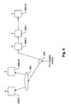
- Scheduler 902 performs three main functions.
- Frame Scheduler 904 maintains and orders queues of frames to be transmitted through the datapath.
- 100 queues 25 each for four priorities
- this number is scalable and could be considerably larger (e.g., 200, 400, etc.) with substantially the same architecture.
- Frame scheduler 904 tracks information on a per frame basis regardless of the size of the frames. Once a frame has been scheduled by Frame Scheduler 904, Subsegment Scheduler 906 schedules the individual subsegments within each frame. Memory Allocation block 908 takes care of memory allocation, i.e., determining where to start storing each frame in the shared memory array 910.
- Scheduler 902 receives frame control information for a particular frame from frame control 912 on the Forward channel. A portion of the frame control information is written into Head Storage 914, and the rest of which proceeds down the pipeline shown to the right of Head Storage 914. Head storage 914 is not required in all implementations, but is used in this implementation to temporarily store portions of the frame control information which are not required to effect the scheduling functions of frame scheduler 904 (e.g., VLAN tagging data). This temporarily stored information is "picked up" again later prior to the functions in which it is utilized. This results in a savings in the sizes of the SRAM arrays in each of the blocks of the Frame Scheduler pipeline. That is, if all the data were copied into blocks 916, 922, etc., it would require more total storage.
- Memory Allocation block 908 maintains a "free" list of each of the 4096 256 byte segments in shared memory array 910 which are not currently in use.
- Head Storage 914 places its portion of the frame control information in one of 4096 slots in its own SRAM array (not shown), each slot corresponding to one of the 4096 segments in shared memory array 910.
- the designated slot corresponds to the location in the shared memory array in which the first segment of a frame is to be stored. If a frame is longer than one segment, Memory Allocation 908 provides a linked list of any additional segments required directly to Subsegment Scheduler 906.
- the address of the frame "head" segment is the unique identifier for each frame in the system.
- the individual SRAM arrays (not shown) in each of Rx Queues 916, Error Storage 918, and Subsegment Scheduler 906 also have 4096 slots which have the same one-to-one correspondence with the 4096 segments in shared memory array 910.
- Head Storage 914 After Head Storage 914 receives the address from Memory Allocation block 908, the frame control information not stored in the Head Storage array propagates along the Frame Scheduler pipeline along with the address information. If the frame is being transmitted in store-and-forward mode, the frame control information sits in a slot in Waiting Room 920 until notification is received that the entire frame has gotten into array 910 (e.g., as indicated by an EOF communicated from Subsegment Scheduler 906 via Error Storage 918), at which point, the frame control information is forwarded to Rx Queues 916. Waiting room has one such slot for each Rx port. If, on the other hand, the frame is being transmitted in cut-through mode, the frame control information proceeds to Rx Queues 916 without being stored in Waiting Room 920.
- the frame control information proceeds to Rx Queues 916 without being stored in Waiting Room 920.
- Rx Queues 916 and Tx Queues 922 include sets of queues in which the frame control information for each frame (referred to from this point forward simply as a "frame") is queued up to await its turn for transmission to the designated Tx port(s).
- the queued up frames in Rx Queues 916 include a destination mask which indicates to which port(s) the frame is to be transmitted.
- Rx Queues 916 is fully provisioned in that it has a slot for each of the 4096 segments in array 910, including the destination mask information.
- Tx Queues 922 is maintained separate from Rx Queues 916 to facilitate multicast of frames, i.e., transmission of a frame from one Rx port to multiple Tx ports.
- different issues arise. For example, if replication occurs only after a frame reaches the head of Rx Queues 916, there is no guarantee that all of the designated Tx ports will be available.
- the queue array would need to be undesirably large in order to ensure that the queue is fully provisioned. Therefore, according to a specific embodiment of the invention, Tx Queues 922 is only fully provisioned for unicast. However, as will be discussed, this is more than sufficient to be able to handle a reasonable multicast requirement.
- each frame in Rx Queues 916 is copied into a slot in Tx Queues 922, with multicast frames being replicated for every port to which they are to be transmitted.
- Each entry in Tx Queues 922 indicates the single Tx port to which the frame is to be transmitted.
- 4096 slots are provided to correspond with the maximum number of frames which can be stored in array 910 at any given time. Unlike the array in Rx Queues 916, these 4096 slots are not indexed to the segments in array 910. As a result, Tx Queues employs its own free list to allocate its slots to incoming frames.
- Maintaining this free list separate from the Memory Allocation Block free list allows the multicast to be more efficient with memory. That is, only a small percentage of the frames in array 910 are likely to be multicast, so creating the second list allows a memory storage on the order of the actual multicast and not the worst case multicast.
- the 4096 slots in Tx Queues 922 although only fully provisioned for unicast, actually provide sufficient space to support a significant multicast requirement because of the fact that the average frame is larger than the 256 bytes segment size in array 910. As a result, there will virtually always be many fewer than 4096 frames stored in the array at any given time. This means that a correspondingly large number of the 4096 slots in Rx Queues 916 are unused at any given time; a sufficiently high number such that even if a significant number of the frames in Rx Queues 916 need to be replicated for multicast, the 4096 slots in Tx Queues are sufficient to hold them all.
- Tx queues there is a credit based flow control mechanism between Rx queues and Tx queues for the 4 fabric priorities. This allows Tx queues to reserve some space (in the corner case where we would run out of space for Tx queues because Tx queues is not fully provisioned) for higher priority multi-cast. If Tx queues were to fill up completely, then it would not result in packet drop, but the forwarding from Tx queues to Rx queues would back up, leading to a small amount of HOL blocking on multicast. This priority mechanism prevents HOL blocking of higher priority in that corner case.
- frames are transmitted according to four different priorities, and Rx Queues 916 has 100 queues organized by Rx port and priority, i.e., one queue for each Rx port per priority.
- Tx Queues 922 also has 100 queues, but organized by Tx port and priority. Thus, for example, if Tx Queues 922 runs out of space for a given priority, multicast frames for a different priority can still be forwarded.
- Tx Queues 922 may be larger or smaller for various implementations. For example, in this implementation a 4096 slot array was chosen because it fully provisions unicast. Alternatively, additional margin against statistically unlikely events may also be provided by increasing the number of slots in Tx Queues 922. In addition, given that Rx Queues 916 is unlikely to ever be completely full, even if Tx Queues 922 becomes full due to a burst of multicast traffic, the unused slots in Rx Queues 916 would still make it unlikely that the system would stall.
- Subsegment Scheduler 906 When Subsegment Scheduler 906 needs a new frame for a particular Tx port, it queries Qcache 924 as to whether a frame is available for that port. Qcache 924 returns a "yes/no" answer. If the answer is "yes,” Qcache 924 also transmits to Subsegment Scheduler 906 the frame control information stored in Tx Queues 922 along with the additional information originally left in Head Storage 914 when the frame entered Frame Scheduler 904. Qcache 924 is maintained separately from Tx Queues 922 in order to be able to keep up with the requests from Subsegment Scheduler 906 which may come in at speeds that Tx Queues 922 might not be able to keep up with.
- the forwarding of a frame involves a request from subsegment scheduler 906, and then the forwarding of frame information stored in Tx Queues and Head storage 914.
- This interaction must happen at a frame rate of 360 MHz in a fully provisioned 24 port switch.
- Qcache 924 is introduced to shorten this latency loop.
- Qcache stores the "top of queue" for 100 queues, which equals ports times priorities.
- Tx Queues 922 which then arranges for the next frame in that port-priority queue to be sent to Qcache from Head Storage 914 and Error Storage 918. This effectively gives two cycles to bring information out of 914, 918, and 922, instead of just one.
- the architecture of the present invention supports strict priority and weighted round robin egress scheduling algorithms.
- QCache determines eligibility from Head Storage, i.e., there is a frame to send at the head of any of the port-priority queues. It receives port availability information from the Subsegment Scheduler. It maintains credit information for all of the priorities within a port. It can then calculate any of a number of different scheduling algorithms locally and efficiently.
- the architecture scales for many new algorithms to be added by a modest modification to Qcache.
- egress scheduling is performed in Qcache 924 based on the egress scheduling algorithm and information from Subsegment Scheduler 906 and the per port flow control. If the frame is eligible (i.e., it is ready for transmission because the frame is to be forwarded in cut-through mode and 64 bytes of the frame have been stored in shared memory array 910, or the frame is in store-and-forward mode and the entire frame has been stored in the shared memory array) and the port is not flow controlled, then it enters the egress scheduling algorithm. Scheduling is implemented in a loop to increase the efficiency of the pipelined circuitry in Qcache 924. A large number of standard scheduling algorithms may be implemented efficiently in this architecture, for example strict priority and weighted round robin. In addition the per port flow control information could have priority information in it, enabling the switch element to respond to priority based flow control.
- Qcache 924 has 100 slots, each for storing the frame at the head of each of the 100 queues in Tx Queues 922. That is, Qcache 924 can store up to four frames for each port, each frame having one of the four different priorities.
- Subsegment Scheduler 906 requests a frame for a particular Tx port
- Qcache 924 sends a frame for that port if it has one in one of the four queues for that port.
- Qcache 924 empties one of its 100 queues, it sends a request to Tx Queues 922 for the next frame in the corresponding one of its 100 queues. This is a particularly scalable aspect of this architecture.
- Tx Queues 922 Assuming that Tx Queues 922 has a frame in that queue, it sends that entry to Qcache 924, but not directly. Rather, Tx Queues 922 sends the frame to Head Storage 914 to pick up the information for that frame stored in Head Storage 914 when the frame originally came into the scheduler. The complete frame control information is then sent to Qcache 924 for storage in the appropriate slot.
- Subsegment Scheduler operates in a loop in which it queries the switch ports in succession as to whether each has something to transmit.
- Subsegment Scheduler 906 is explicitly disallowed to request a new frame for a particular port from Qcache 924 on successive passes through the loop. This smoothes out the burstiness in Subsegment Scheduler 906 and SRAM array 910 which would otherwise be associated with beginning a new minimum-size (i.e., 64 byte) frame on every cycle. This in turn reduces the amount of buffering required as well as the jitter caused by such bursts.
- the entry stored in Qcache may also include error information for the frame received from Error Storage 918.
- the purpose of Error Storage 918 is to facilitate suppression of frames with errors when operating in store-and-forward mode. If a frame has come into the array completely, Error Storage 918 stores an error bit indicating whether the Rx port by which the frame arrived marked it with an error. This mechanism allows the error information of a frame to be propagated from the end of the frame to the beginning of the frame. This information is then used by Subsegment Scheduler 906 to facilitate suppression of the frame.
- the error information received by Subsegment Scheduler 906 (TE in Fig. 9 ) is simply passed to the Tx port for egress tag processing.
- the frame's CRC may or may not be negated depending upon the nature of the error. If the error is a result of the CRC itself being bad, then the frame is allowed to go out with the same CRC. Alternatively, if the error corresponds to something else in the frame, the CRC is negated before the frame goes out, e.g., in the Tx port.
- Error Storage 918 allows the Subsegment Scheduler to facilitate frame suppression in store-and-forward mode. However, if frame transmission begins before the EOF has been received, (e.g., as in cut-through mode), the information in Error Storage 918 should be ignored. Therefore, according to a specific embodiment, a locking mechanism is provided which detects whether Error Storage 918 is being read for a particular frame before the error bits for that frame have been written.
- One way to implement such a locking mechanism is to provide an error bit and a validity bit in Error Storage 918.
- the validity bit would start out as invalid.
- the error bit would be set accordingly and the validity bit would be set to valid to indicate that the error information is current.
- Subsegment Scheduler 906 reads a frame from Qcache 924, it would look at the validity bit to determine whether or not to ignore the error bit.
- the polarity of the validity bit is employed to determine whether the associated error information is valid. That is, each time the validity bit is used, it is toggled to the opposite state. This is then compared with the "polarity" of the frame (actually the first segment of the frame) to determine whether the error bit is valid.
- the polarity of the frame is represented by a polarity bit in the free list entry in Memory Allocation block 908 which corresponds to the first segment of the frame.
- the free list entry for each frame also includes a second polarity bit which is employed by Subsegment Scheduler 906 to ensure that reading of subsegments does not begin before they are written to the array.
- the implementation of this is a straight forward locking mechanism. If for any of the 4 subsegments per each segment stored in the memory, the locking bits stored in the subsegment scheduler do not match the same polarity as was recorded in the free list, then the data have not yet been written into the array, and subsegment scheduler will wait for it before scheduling that data.
- this locking mechanism only a few bits per frame in the subsegment scheduler need to operate at the subsegment rate. This rate is twice the frame rate, and allows the switch to perform cut-through on 64 byte subsegments, leading to a very low latency switch.
- Subsegment Scheduler 906 "loops through" all of the switch ports, servicing both the Rx and Tx portions of each port in turn.
- Subsegment Scheduler 906 includes a 4096 slot SRAM which is indexed by the 4096 segments in array 910.
- the array in Subsegment Scheduler 906 is organized by segment, storing linked lists of segments, padding information which indicates how many bytes are valid in the last subsegment of a segment, and a reference count, the use of which is described below.
- the SRAM array in Subsegment Scheduler 906 is implemented as a dual-ported SRAM to provide sufficient margin for the required read and write speeds.
- the SRAM array in Subsegment Scheduler 906 is implemented as a dual-ported 10T SRAM array as described in U.S. Patent Application 10/890,816 (Attorney Docket No. FULCP008).
- Memory Allocation 908 provides a beginning segment address to Head Storage 914 for each port (e.g., 25 different segment addresses for the 25 port embodiments discussed above). Head Storage 914 then provides these segment address pointers to Subsegment Scheduler 906 so that Subsegment Scheduler 906 has a starting segment allocated for each port before any frames are received. Thus, when the first subsegment for a frame is received on a particular Rx port, Subsegment Scheduler 906 can already read the pre-allocated segment address for that Rx port. When Head Storage 914 receives the frame control information on the Forward channel and uses the pre-allocated address as described above, it also gets another pre-allocated address from Memory Allocation 908 to present to Subsegment Scheduler 906 for that Rx port.
- Head Storage 914 receives the frame control information on the Forward channel and uses the pre-allocated address as described above, it also gets another pre-allocated address from Memory Allocation 908 to present to Subsegment Scheduler 906
- Segments in SRAM array 910 are freed for reuse (i.e., placed back in the free list in Memory Allocation 908) when their data are sent out to a Tx port.
- segments of a particular frame are discarded, they are not sent to a Tx port, so another mechanism must be provided to free those addresses.
- One such mechanism uses a special discard Tx unit which spools the addresses back to the free list as if the discarded segments had been transmitted to that "port.”
- Head Storage 914 provides a discard bit to Subsegment Scheduler for each Rx port which indicates whether a frame received on that port is going to be discarded.
- This discard bit is derived from the frame control information sent on the Forward channel which includes a destination mask of all zeros. Because the first segment for a particular frame has already been allocated as described above, the first four subsegments received for a frame (regardless of whether or not the frame has been marked for discarding) are written to the allocated segment.
- Subsegment Scheduler 906 After some number (e.g., 3 or 4) of the subsegments of the first segment have been received (providing sufficient time to allow the discard bit to be set), Subsegment Scheduler 906 reads the discard bit provided by Head Storage 914 to determine whether further segments in array 910 should be allocated for this frame. Subsegment Scheduler 906 then acknowledges this discard with a completion signal sent back to Head Storage 914. This prevents a future frame from being scheduled that would use the same address. The acknowledgement scheme prevents a race condition.
- the discard bit indicates that the frame is to be discarded, no further segments are allocated for that frame. Rather, the first segment which has already been allocated is simply reused with subsequent subsegments being written over the previously received subsegments for that frame. Thus, only a single segment in array 910 gets allocated for a frame which is going to be discarded. When the writing to that segment for the frame to be discarded is complete, that segment is used as the pre-allocated segment for that port for the next frame. In this way, a separate mechanism for freeing up a segment is not required.
- the segments in array 910 used to store the subsegments of that frame are freed for reuse as the contents of each segment are transmitted to a Tx port.
- a frame is being multicast, its segments should not be freed after transmission to a single Tx port. That is, the segments should only be freed upon transmission to the final Tx port to which the frame is being multicast. Therefore, a reference count is maintained which tracks whether the frame has been transmitted to the requisite number of Tx ports.
- This count could be determined for each segment from, for example, the destination mask received by Head Storage 914 via the Forward channel. That is, each time Subsegment Scheduler 906 facilitates transmission of a particular segment to a Tx port, it could notify Memory Allocation 908 which could then decrement the count. When the reference count reached zero, Memory Allocation 908 could then return the segment to the free list.
- the number added to the reference count for all but one of the ports to which a segment is transmitted is 1.
- the number representing transmission to the remaining port is whatever is needed to get the counter back to zero.
- the count wraps around to zero, indicating that the segment may be returned to the free list.
- the number can either be zero or, alternatively, the total count for the counter, e.g., 64 for a 6-bit counter.
- the numbers to be added to the reference count are determined at the time of multicast replication between Rx Queues 916 and Tx Queues 922. That is, when Rx Queues 916 is doing the multicast replication, it determines the necessary reference count contributions with reference to the destination bit mask, and includes these numbers with the Tx Queues entries. So, for each entry in Tx Queues, there is a reference count contribution number which is provided to Subsegment Scheduler 906 via Qcache 924 as described above, and eventually to Memory Allocation 908.
- the frame discard mechanism described above relies on information received from the frame control which indicates that a frame is to be discarded. However, there are other cases in which a frame may need to be discarded that will not be indicated in the frame control information. For example, a frame may have an error as indicated by the EOF which typically does not come in before the frame control information. As described above, such an error is only made apparent when the frame entry is in Qcache 924.
- the Ethernet spec imposes a time out requirement which specifies a maximum time that a frame is allowed to "live" in the switch. When that time is exceeded (e.g., as a result of a port asserting the Pause control to Qcache 924 or bursts of high priority traffic stalling lower priority traffic), the frame must be discarded.
- a time stamp which Qcache uses to determine if any of the frames in its slots have become stale.
- Subsegment Scheduler 906 discards these frames.
- segments in array 910 are typically returned to the free list in Memory Allocation 908 only after all of the subsegments have been transmitted to the Tx port.
- the entire first segment which had been allocated can be discarded at once. If successive frames are discarded, this can result in segments being freed at a rate faster than that for which Memory Allocation 908 is provisioned. Therefore a FIFO 926 and throttling mechanism is provided between Subsegment Scheduler 906 and Memory Allocation 908 to deal with this condition.
- a token When a token is sent from Subsegment Scheduler 906 to Memory Allocation 908 as a result of a successfully transmitted segment to one or more Tx ports, it is inserted into FIFO 926 unconditionally. However, when the token is being sent because a frame was discarded, Subsegment Scheduler 906 queries FIFO 926 to determine whether there is room in the FIFO to receive the token. If so, the token is transmitted to FIFO 926. If not, then Subsegment Scheduler 906 waits until the next time through the loop (i.e., the next time it is servicing the port for which the frame was originally intended) to query FIFO 926 again. This continues until FIFO 926 has room. Eventually, the token reaches Memory Allocation 908 and the corresponding segment is returned to the free list.
- Memory Allocation 908 reports status information on the channel "Status" from the scheduler to frame control 912 for the processing of congestion management policies.
- the frame processor may use this information to centralize the computation of complex congestion management policies in an efficient manner. This further allows the forwarding information from 912 to 914 to include the results of the congestion management processing.
- Such processing may include, weighted random early discard, tail discard, the generation of Tx (or egress) pause signals to neighboring switches, the generation of explicit congestion notification, either forward or backward, and other forms of congestion management.
- the memory allocation of shared memory array 910 uses 256 Byte segments, the status may be reported based on any other fundamental segment size. For example one implementation uses a 1024 byte segment size to reduce the event rate of the status channel.
- frames are associated with multiple logical queues. Each queue does not need reserved physical memory, and a frame may be associated with multiple queues provided that 1) the ingress crossbar is non-blocking, 2) the congestion management calculations are applied while the frames are stored in the shared memory, and 3) ordering is maintained for data within a frame by the linked list, and 4) for frames within each egress scheduling queue by 922 and 924. All of these conditions are required to allow multiple queue association in the specific implementation shown.
- a new frame is associated with an Rx Port on ingress through the crossbar, a Tx port once the forwarding information has been received from 912, and with the total memory.
- Frame control 912 may contain many watermarks for congestion management processing against which the status information is checked. In particular, it may include a notion of a private allocation for each port, and then create a "shared pool" value as the total memory minus the sum of each port's private memory. Rx port status above the Rx private watermark contributes to the shared pool, and then it contributes the difference.
- Another implementation could generate status information based on the priority with which each frame is associated, and use that for congestion management processing based on either port priority or a global priority as well, that is the sum of every port's packets of the same priority within the switch.
Landscapes
- Engineering & Computer Science (AREA)
- Multimedia (AREA)
- Computer Networks & Wireless Communication (AREA)
- Signal Processing (AREA)
- Data Exchanges In Wide-Area Networks (AREA)
- Multi Processors (AREA)
- Use Of Switch Circuits For Exchanges And Methods Of Control Of Multiplex Exchanges (AREA)
- Electronic Switches (AREA)
Claims (39)
- Gemeinschaftsspeicher umfassend:mehrere Empfangsanschlüsse (104), welche durch eine erste Datenrate gekennzeichnet sind;mehrere Sendeanschlüsse (108), welche durch die erste Datenrate gekennzeichnet sind;eine Speicheranordnung (106), welche mehrere Speicherbänke umfasst, welche in Zeilen und Spalten organisiert sind, wobei ein Betrieb der Speicheranordnung (106) durch eine zweite Datenrate gekennzeichnet ist;einen nicht blockierenden Empfangskreuzschienenschaltkreis (102), welcher ausgestaltet ist, einen beliebigen der Eingangsanschlüsse (104) mit einer beliebigen der Speicherbänke zu verbinden;einen nicht blockierenden Sendekreuzschienenschaltkreis (110), welcher ausgestaltet ist, eine beliebige der Speicherbänke mit einem beliebigen der Sendeanschlüsse (108) zu verbinden;eine Pufferung, welche ausgestaltet ist, einen Betrieb der Empfangs- und Sendeanschlüsse (104, 108) mit der ersten Datenrate von einem Betrieb der Speicheranordnung (106) mit der zweiten Datenrate zu entkoppeln; undeinen Planungsschaltkreis (114), welcher ausgestaltet ist, ein Zusammenspiel der Anschlüsse (104, 108), des Kreuzschienenschaltkreises (102, 110) und der Speicheranordnung (106) zu steuern, um ein Speichern und Abfragen von Datensegmenten in dem Gemeinschaftsspeicher zu bewirken, wobei der Planungsschaltkreis (114) ausgestaltet ist, ein Anordnen eines jeden Datensegments eines Rahmens über die Speicherbänke in eine der Reihen zu unterstützen, und ein Anordnen von aufeinanderfolgenden Datensegmenten des Rahmens über aufeinanderfolgende Reihen in der Anordnung (106) zu unterstützen.
- Gemeinschaftsspeicher nach Anspruch 1, wobei ein Betrieb des Empfangs- und des Sendekreuzschienenschaltkreises (102, 110) durch eine dritte Datenrate gekennzeichnet ist, und wobei die Pufferung erste Puffer zwischen jedem Empfangsanschluss (104) und dem Empfangskreuzschienenschaltkreis (102) und zweite Puffer zwischen jedem Sendeanschluss (108) und dem Sendekreuzschienenschaltkreis (110) aufweist, wobei die ersten und zweiten Puffer ausgestaltet sind, einen Betrieb der Sende- und Empfangsanschlüsse (104, 108) bei der ersten Datenrate von einem Betrieb des Sende- und des Empfangskreuzschienenschaltkreises (102, 110) bei der dritten Datenrate zu entkoppeln.
- Gemeinsamer Speicher nach Anspruch 2, wobei jeder der ersten Puffer ausgestaltet ist, ein gesamtes Segment eines Rahmens zu speichern.
- Gemeinschaftsspeicher nach Anspruch 2, wobei jeder der zweiten Puffer ausreichend groß ist, um sämtlichen Jitter durch den Gemeinschaftsspeicher zu berücksichtigen.
- Gemeinschaftsspeicher nach Anspruch 1, wobei ein Betrieb des Empfangs- und des Sendekreuzschienenschaltkreises (102, 110) durch eine dritte Datenrate gekennzeichnet ist, und wobei die Pufferung erste Puffer zwischen dem Empfangskreuzschienenschaltkreis (102) und jeder der Speicherbänke und zweite Puffer zwischen dem Sendekreuzschienenschaltkreis (110) und jeder der Speicherbänke aufweist, wobei die ersten und zweiten Puffer ausgestaltet sind, einen Betrieb der Speicheranordnung (106) bei der zweiten Datenrate von einem Betrieb des Empfangs- und des Sendekreuzschienenschaltkreises (102, 110) bei der dritten Datenrate zu entkoppeln.
- Gemeinschaftsspeicher nach Anspruch 1, wobei der Planungsschaltkreis (114) ausgestaltet ist, ein Anordnen von jedem Datensegment über die Speicherbänke in einer Reihe zu unterstützen, indem der Empfangskreuzschienenschaltkreis (102) angesteuert wird, jedes aufeinanderfolgende Wort eines jeden Datensegments über aufeinanderfolgende Ausgangsanschlüsse des Empfangskreuzschienenschaltkreises (102) zu übertragen.
- Gemeinschaftsspeicher nach Anspruch 6, wobei von dem Empfangskreuzschienenschaltkreis (102) nur einmal pro Datensegment eine willkürliche Entscheidung gefällt wird.
- Gemeinschaftsspeicher nach Anspruch 1, wobei der Planungsschaltkreis (114) ausgestaltet ist, den Sendekreuzschienenschaltkreis (110) anzusteuern, jedes aufeinanderfolgende Wort eines jeden Datensegments über aufeinanderfolgende Eingangsanschlüsse des Sendekreuzschienenschaltkreises (110) zu empfangen.
- Gemeinschaftsspeicher nach Anspruch 8, wobei von dem Sendekreuzschienenschaltkreis (110) nur einmal pro Datensegment eine willkürliche Entscheidung gefällt wird.
- Gemeinschaftsspeicher nach Anspruch 1, wobei der Planungsschaltkreis (114) ausgestaltet ist, eine erste der Reihen der Speicherbänke für ein Anordnen eines Anfangssegments eines jeden Rahmens auszuwählen, wobei das Auswählen der ersten Reihe entweder pseudozufällig oder deterministisch durchgeführt wird.
- Gemeinschaftsspeicher nach Anspruch 10, wobei das Auswählen der ersten Reihe deterministisch ausgeführt wird, wobei die erste Reihe aus den Reihen der Speicherbänke in einer linearen Reihenfolge ausgewählt wird.
- Gemeinschaftsspeicher nach Anspruch 10, wobei das Auswählen der ersten Reihe deterministisch ausgeführt wird, wobei die erste Reihe aus den Reihen von Speicherbänken gemäß einem Algorithmus ausgewählt wird, welcher die in letzter Zeit am wenigsten zugeordnete auswählt.
- Gemeinschaftsspeicher nach Anspruch 1, wobei der Empfangskreuzschienenschaltkreis (102) und der Sendekreuzschienenschaltkreis (110) mehrere Kreuzschienen umfassen, welche in mehreren Stufen angeordnet sind.
- Gemeinschaftsspeicher nach Anspruch 13, wobei die mehreren Kreuzschienen des Empfangskreuzschienenschaltkreises (102) mehrere Eingangskreuzschienen umfassen, und wobei jeder der Empfangsanschlüsse (104) des Gemeinschaftsspeichers einem der Eingangskreuzschienen zugeordnet ist.
- Gemeinschaftsspeicher nach Anspruch 14, wobei die mehreren Eingangskreuzschienen zwei Eingangskreuzschienen von gleicher Größe umfassen, und wobei eine Hälfte der Empfangsanschlüsse (104) jedem der Eingangskreuzschienen zugeordnet ist.
- Gemeinschaftsspeicher nach Anspruch 13, wobei die mehreren Kreuzschienen des Sendekreuzschienenschaltkreises (110) mehrere Ausgangskreuzschienen umfassen, und wobei jeder der Sendeanschlüsse (108) des Gemeinschaftsspeichers einer der Ausgangskreuzschienen zugeordnet ist.
- Gemeinschaftsspeicher nach Anspruch 16, wobei die mehreren Ausgangskreuzschienen zwei Ausgangskreuzschienen von gleicher Größe umfassen, und wobei eine Hälfte der Sendeanschlüsse (108) jeder der Ausgangskreuzschienen zugeordnet ist.
- Gemeinschaftsspeicher nach Anspruch 13, wobei der Empfangskreuzschienenschaltkreis (102) mindestens eine Eingangskreuzschiene umfasst, welche einen Eingang, der jedem der Empfangsanschlüsse (104) zugeordnet ist, und einen Ausgang, der jedem der Spalten in der Speicheranordnung (106) zugeordnet ist, aufweist, wobei der Empfangskreuzschienenschaltkreis (102) ferner mehrere Spaltenkreuzschienen umfasst, wobei jede davon mindestens einer der Spalten in der Speicheranordnung (106) zugeordnet ist und ausgestaltet ist, mindestens einen der Eingangskreuzschienenausgänge mit den Speicherbänken in der zugeordneten Spalte zu verbinden.
- Gemeinschaftsspeicher nach Anspruch 13, wobei der Sendekreuzschienenschaltkreis (110) mindestens eine Ausgangskreuzschiene umfasst, welche einen Ausgang, der jedem der Sendeanschlüsse (108) zugeordnet ist, und einen Eingang, welcher jeder der Spalten in der Speicheranordnung (106) zugeordnet ist, aufweist, wobei der Sendekreuzschienenschaltkreis (110) ferner mehrere Spaltenkreuzschienen umfasst, wobei jede von diesen mindestens eine der Spalten in der Speicheranordnung (106) zugeordnet ist und ausgestaltet ist, mindestens einen der Ausgangskreuzschieneneingänge mit den Speicherbänken in der zugeordneten Spalte zu verbinden.
- Gemeinschaftsspeicher nach Anspruch 1, ferner umfassend eine Empfangsanschlusslogik, welche jedem Empfangsanschluss zugeordnet ist und welche ausgestaltet ist, eine Steuerinformation von den Datensegmenten für eine Verwendung durch den Planungsschaltkreis (114) beim Ausführen des Speicherns der Datensegmente in der Speicheranordnung (106) zu trennen.
- Gemeinschaftsspeicher nach Anspruch 20, ferner umfassend eine Sendeanschlusslogik, welche jedem Sendeanschluss (108) zugeordnet ist und welche ausgestaltet ist, die Steuerinformation mit den Datensegmenten für eine Übertragung auf dem zugeordneten Sendeanschluss (108) wieder zu kombinieren.
- Gemeinschaftsspeicher nach Anspruch 20, wobei die Steuerinformation eine gesamte Steuerinformation umfasst, welche den Datensegmenten zugeordnet ist, und wobei nur Nutzlastdaten, welche den Datensegmenten zugeordnet sind, in der Speicheranordnung (106) gespeichert werden.
- Gemeinschaftsspeicher nach Anspruch 20, wobei zumindest einige der Steuerinformationen in der Speicheranordnung (106) zusammen mit Nutzlastdaten, welche den Datensegmenten zugeordnet sind, gespeichert werden.
- Gemeinschaftsspeicher nach Anspruch 23, wobei die Steuerinformation eine Länge für das zugeordnete Datensegment kodiert und ein Ende-des-Rahmens-Bit oder ein Fehler-Bit aufweist.
- Gemeinschaftsspeicher nach Anspruch 1, ferner umfassend einen Rahmensteuerschaltkreis (112), welcher ausgestaltet ist, eine Verarbeitung auf Rahmenebene für jeden der Rahmen bereitzustellen, wobei der Empfangs- und der Sendekreuzschienenschaltkreis (102, 110), die Speicheranordnung (106), mindestens etwas von der Pufferung, der Planungsschaltkreis (114), ein erster Anteil von jeweils den Empfangs- und den Sendeanschlüssen (104, 108) und ein erster Anteil von dem Rahmensteuerschaltkreis (112) einen asynchronen Schaltkreis umfassen, welcher in einem asynchronen Bereich arbeitet, und wobei ein übriger Anteil von jeweils den Empfangs- und den Sendeanschlüssen (104, 108) und ein übriger Anteil des Rahmensteuerschaltkreises (112) einen synchronen Schaltkreis umfassen, welcher in einem synchronen Bereich arbeitet.
- Gemeinschaftsspeicher nach Anspruch 25, wobei der synchrone Schaltkreis des Gemeinschaftsspeichers ermöglicht, dass der Gemeinschaftsspeicher als ein synchroner Block in einem synchronen System arbeitet.
- Gemeinschaftsspeicher nach Anspruch 1, wobei jedes Datensegment mehrere Untersegmente umfasst, und wobei der Planungsschaltkreis (114) ausgestaltet ist, eine Bewegung eines jeden einzelnen Untersegments durch den Gemeinschaftsspeicher zu ermöglichen, während jedem Datensegment nur einmal ein Platz in der Speicheranordnung (106) zugeordnet wird.
- Gemeinschaftsspeicher nach Anspruch 27, wobei jedes Datensegment 256 Bytes umfasst und jedes Untersegment 64 Bytes umfasst.
- Gemeinschaftsspeicher nach Anspruch 1, wobei der Planungsschaltkreis (114) ausgestaltet ist, ein Verarbeiten von Rahmen mit veränderlicher Länge zu ermöglichen.
- Gemeinschaftsspeicher nach Anspruch 29, wobei der Planungsschaltkreis (114) ausgestaltet ist, einen Betrieb des Gemeinschaftsspeichers in einer Speichern-und-Weiterleiten-Betriebsart und/oder einer Durchschneidebetriebsart (Cut-Through-Betriebsart) zu ermöglichen.
- Gemeinschaftsspeicher nach Anspruch 1, wobei der Planungsschaltkreis (114) ausgestaltet ist, ein Speichern eines ersten Datensegments in der Speicheranordnung (106) und ein Abfragen eines zweiten Datensegments aus der Speicheranordnung (106) im Wesentlichen gleichzeitig zu ermöglichen, wobei das erste und das zweite Datensegment ohne Bezug sind.
- Gemeinschaftsspeicher nach Anspruch 31, wobei der Planungsschaltkreis (114) ausgestaltet ist, unabhängige Steuerströme für den Empfangs- und den Sendekreuzschienenschaltkreis (102, 110) zu erzeugen.
- Gemeinschaftsspeicher nach Anspruch 32, wobei jeder von dem Empfangs- und dem Sendekreuzschienenschaltkreis (102, 110) zwei unabhängige Kreuzschienen umfasst, wobei einer der unabhängigen Steuerströme jeder zugeordnet ist.
- Gemeinschaftsspeicher nach Anspruch 1, wobei der Empfangskreuzschienenschaltkreis (102) mehrere Eingangskanäle und mehrere Ausgangskanäle umfasst, und wobei der Sendekreuzschienenschaltkreis (110) mehrere Eingangskanäle und mehrere Ausgangskanäle umfasst, wobei der Planungsschaltkreis (114) ausgestaltet ist, Steuerdaten für die Eingangskanäle des Empfangskreuzschienenschaltkreises (102) und die Ausgangskanäle des Sendekreuzschienenschaltkreises (110) zu serialisieren und Steuerdaten für die Ausgangskanäle des Empfangskreuzschienenschaltkreises (102) und die Eingangskanäle des Sendekreuzschienenschaltkreises (110) zu parallelisieren.
- Gemeinschaftsspeicher nach Anspruch 1, wobei die Pufferung einen Ausgangspuffer aufweist, welcher jedem der Sendeanschlüsse (108) zugeordnet ist, wobei jeder Sendeanschluss (108) ausgestaltet ist, zu warten, um Datensegmente eines Rahmens von dem zugeordneten Ausgangspuffer zu empfangen bis eine erste Anzahl von Datensegmenten des Rahmens in dem Ausgangspuffer gespeichert worden ist.
- Gemeinschaftsspeicher nach Anspruch 35, wobei die erste Anzahl in Bezug auf die erste Datenrate bestimmt ist.
- Gemeinschaftsspeicher nach Anspruch 35, wobei jeder Sendeanschluss (108) ferner ausgestaltet ist, ein Empfangen der Datensegmente des Rahmens zu beginnen, wenn eines der in dem zugeordneten Ausgangspuffer gespeicherten Datensegmente ein Ende des Rahmens anzeigt.
- Switch umfassend den Gemeinschaftsspeicher nach Anspruch 1 und mit einem zugeordneten Schaltprotokoll.
- Switch nach Anspruch 38, wobei das Schaltprotokoll Ethernet umfasst.
Applications Claiming Priority (3)
| Application Number | Priority Date | Filing Date | Title |
|---|---|---|---|
| US64379405P | 2005-01-12 | 2005-01-12 | |
| US11/208,451 US7814280B2 (en) | 2005-01-12 | 2005-08-18 | Shared-memory switch fabric architecture |
| PCT/US2006/000326 WO2006076204A2 (en) | 2005-01-12 | 2006-01-05 | Shared-memory switch fabric architecture |
Publications (3)
| Publication Number | Publication Date |
|---|---|
| EP1839166A2 EP1839166A2 (de) | 2007-10-03 |
| EP1839166A4 EP1839166A4 (de) | 2009-03-04 |
| EP1839166B1 true EP1839166B1 (de) | 2009-12-23 |
Family
ID=36654613
Family Applications (1)
| Application Number | Title | Priority Date | Filing Date |
|---|---|---|---|
| EP06717512A Expired - Lifetime EP1839166B1 (de) | 2005-01-12 | 2006-01-05 | Schaltmatrixarchitektur eines gemeinsamen speichers |
Country Status (6)
| Country | Link |
|---|---|
| US (2) | US7814280B2 (de) |
| EP (1) | EP1839166B1 (de) |
| JP (1) | JP4667469B2 (de) |
| AT (1) | ATE453154T1 (de) |
| DE (1) | DE602006011272D1 (de) |
| WO (1) | WO2006076204A2 (de) |
Families Citing this family (42)
| Publication number | Priority date | Publication date | Assignee | Title |
|---|---|---|---|---|
| US20040085904A1 (en) * | 2002-10-31 | 2004-05-06 | Bordogna Mark A. | Method for flow control of packets aggregated from multiple logical ports over a transport link |
| EP1987428A2 (de) * | 2006-02-24 | 2008-11-05 | Mbda Uk Limited | Verteilte echtzeit-prozessorumgebung |
| US7280398B1 (en) * | 2006-08-31 | 2007-10-09 | Micron Technology, Inc. | System and memory for sequential multi-plane page memory operations |
| US20080155187A1 (en) * | 2006-12-20 | 2008-06-26 | Maurizio Skerlj | System including memory buffer configured to decouple data rates |
| US7916718B2 (en) * | 2007-04-19 | 2011-03-29 | Fulcrum Microsystems, Inc. | Flow and congestion control in switch architectures for multi-hop, memory efficient fabrics |
| US20090019184A1 (en) * | 2007-07-10 | 2009-01-15 | Qimonda Ag | Interfacing memory devices |
| US8356138B1 (en) * | 2007-08-20 | 2013-01-15 | Xilinx, Inc. | Methods for implementing programmable memory controller for distributed DRAM system-in-package (SiP) |
| US20090063807A1 (en) * | 2007-08-29 | 2009-03-05 | International Business Machines Corporation | Data redistribution in shared nothing architecture |
| EP2068561A1 (de) | 2007-11-29 | 2009-06-10 | Deutsche Thomson OHG | Verfahren und Vorrichtung zur Aufzeichnung von Rahmen |
| US8370557B2 (en) * | 2008-12-19 | 2013-02-05 | Intel Corporation | Pseudo dual-port SRAM and a shared memory switch using multiple memory banks and a sideband memory |
| US8126002B2 (en) * | 2009-03-31 | 2012-02-28 | Juniper Networks, Inc. | Methods and apparatus related to a shared memory buffer for variable-sized cells |
| US8644140B2 (en) * | 2009-09-09 | 2014-02-04 | Mellanox Technologies Ltd. | Data switch with shared port buffers |
| US8873377B2 (en) | 2009-11-18 | 2014-10-28 | Juniper Networks, Inc. | Method and apparatus for hitless failover in networking systems using single database |
| JP5333200B2 (ja) * | 2009-12-25 | 2013-11-06 | 富士通株式会社 | パケット通信制御装置、メモリアクセス制御装置及び情報処理システム |
| US8441922B1 (en) * | 2010-10-05 | 2013-05-14 | Qlogic, Corporation | Method and system for congestion management in networks |
| US8699491B2 (en) | 2011-07-25 | 2014-04-15 | Mellanox Technologies Ltd. | Network element with shared buffers |
| KR101292309B1 (ko) * | 2011-12-27 | 2013-07-31 | 숭실대학교산학협력단 | 반도체칩 및 메모리 제어방법, 그리고 그 방법을 컴퓨터에서 실행시키기 위한 프로그램을 기록한 기록매체 |
| WO2013167973A2 (en) * | 2012-05-10 | 2013-11-14 | Marvell World Trade Ltd. | Hybrid dataflow processor |
| US9438537B2 (en) | 2012-07-03 | 2016-09-06 | Freescale Semiconductor, Inc. | Method for cut through forwarding data packets between electronic communication devices |
| US9582440B2 (en) | 2013-02-10 | 2017-02-28 | Mellanox Technologies Ltd. | Credit based low-latency arbitration with data transfer |
| US8989011B2 (en) | 2013-03-14 | 2015-03-24 | Mellanox Technologies Ltd. | Communication over multiple virtual lanes using a shared buffer |
| US9189435B2 (en) * | 2013-04-23 | 2015-11-17 | Apple Inc. | Method and apparatus for arbitration with multiple source paths |
| US9535832B2 (en) * | 2013-04-30 | 2017-01-03 | Mediatek Singapore Pte. Ltd. | Multi-hierarchy interconnect system and method for cache system |
| US9641465B1 (en) | 2013-08-22 | 2017-05-02 | Mellanox Technologies, Ltd | Packet switch with reduced latency |
| US9548960B2 (en) | 2013-10-06 | 2017-01-17 | Mellanox Technologies Ltd. | Simplified packet routing |
| US9325641B2 (en) | 2014-03-13 | 2016-04-26 | Mellanox Technologies Ltd. | Buffering schemes for communication over long haul links |
| KR102106261B1 (ko) | 2014-06-17 | 2020-05-04 | 삼성전자주식회사 | 메모리 컨트롤러의 작동 방법과 이를 포함하는 장치들의 작동 방법들 |
| US9584429B2 (en) | 2014-07-21 | 2017-02-28 | Mellanox Technologies Ltd. | Credit based flow control for long-haul links |
| CN104852863B (zh) * | 2015-04-15 | 2018-04-10 | 清华大学 | 一种共享缓存交换机中的动态阈值管理方法及装置 |
| US10326606B2 (en) * | 2016-02-18 | 2019-06-18 | Media Links Co., Ltd. | Multicast switching system |
| US10277533B2 (en) * | 2016-11-18 | 2019-04-30 | International Business Machines Corporation | Cut-through bridge error isolation |
| US10176857B1 (en) * | 2017-06-22 | 2019-01-08 | Globalfoundries Inc. | Read and write scheme for high density SRAM |
| US11489789B2 (en) * | 2018-06-29 | 2022-11-01 | Intel Corporation | Technologies for adaptive network packet egress scheduling |
| US10951549B2 (en) | 2019-03-07 | 2021-03-16 | Mellanox Technologies Tlv Ltd. | Reusing switch ports for external buffer network |
| US11171884B2 (en) | 2019-03-13 | 2021-11-09 | Mellanox Technologies Tlv Ltd. | Efficient memory utilization and egress queue fairness |
| US11470010B2 (en) | 2020-02-06 | 2022-10-11 | Mellanox Technologies, Ltd. | Head-of-queue blocking for multiple lossless queues |
| US11558316B2 (en) | 2021-02-15 | 2023-01-17 | Mellanox Technologies, Ltd. | Zero-copy buffering of traffic of long-haul links |
| US12474833B2 (en) | 2021-11-02 | 2025-11-18 | Mellanox Technologies, Ltd | Queue bandwidth estimation for management of shared buffers and allowing visibility of shared buffer status |
| JP7537769B2 (ja) | 2022-01-12 | 2024-08-21 | Necプラットフォームズ株式会社 | シリアルインタフェース回路、その制御方法、プログラム、通信モジュール及び通信装置 |
| US11973696B2 (en) | 2022-01-31 | 2024-04-30 | Mellanox Technologies, Ltd. | Allocation of shared reserve memory to queues in a network device |
| US11876726B2 (en) * | 2022-03-07 | 2024-01-16 | Nxp B.V. | Disabling cut-through frame transfer based on a cycle time period and apparatus for disabling |
| US12375404B2 (en) | 2022-08-25 | 2025-07-29 | Mellanox Technologies, Ltd | Flow-based congestion control |
Family Cites Families (55)
| Publication number | Priority date | Publication date | Assignee | Title |
|---|---|---|---|---|
| US4680701A (en) * | 1984-04-11 | 1987-07-14 | Texas Instruments Incorporated | Asynchronous high speed processor having high speed memories with domino circuits contained therein |
| GB8711991D0 (en) * | 1987-05-21 | 1987-06-24 | British Aerospace | Asynchronous communication systems |
| US4912348A (en) * | 1988-12-09 | 1990-03-27 | Idaho Research Foundation | Method for designing pass transistor asynchronous sequential circuits |
| US5752070A (en) * | 1990-03-19 | 1998-05-12 | California Institute Of Technology | Asynchronous processors |
| JP2583679B2 (ja) * | 1990-07-06 | 1997-02-19 | 三菱電機株式会社 | セル交換装置 |
| US5121003A (en) | 1990-10-10 | 1992-06-09 | Hal Computer Systems, Inc. | Zero overhead self-timed iterative logic |
| US5434520A (en) * | 1991-04-12 | 1995-07-18 | Hewlett-Packard Company | Clocking systems and methods for pipelined self-timed dynamic logic circuits |
| US5367638A (en) * | 1991-12-23 | 1994-11-22 | U.S. Philips Corporation | Digital data processing circuit with control of data flow by control of the supply voltage |
| DE4214981A1 (de) * | 1992-05-06 | 1993-11-11 | Siemens Ag | Asynchrone Logikschaltung für den 2-Phasen-Betrieb |
| DE69430352T2 (de) * | 1993-10-21 | 2003-01-30 | Sun Microsystems Inc., Mountain View | Gegenflusspipeline |
| US5440182A (en) * | 1993-10-22 | 1995-08-08 | The Board Of Trustees Of The Leland Stanford Junior University | Dynamic logic interconnect speed-up circuit |
| US6152613A (en) * | 1994-07-08 | 2000-11-28 | California Institute Of Technology | Circuit implementations for asynchronous processors |
| US5642501A (en) * | 1994-07-26 | 1997-06-24 | Novell, Inc. | Computer method and apparatus for asynchronous ordered operations |
| US5732233A (en) * | 1995-01-23 | 1998-03-24 | International Business Machines Corporation | High speed pipeline method and apparatus |
| DE69621763T2 (de) * | 1995-08-23 | 2003-02-06 | Koninklijke Philips Electronics N.V., Eindhoven | Datenverarbeitungssystem mit einer asynchrongesteuerten pipeline |
| EP0882357B1 (de) * | 1996-01-03 | 2004-07-21 | Sony Electronics, Inc. | Kopiergeschütztes aufnahme- und wiedergabesystem |
| JP3156752B2 (ja) * | 1996-02-09 | 2001-04-16 | 日本電気株式会社 | Atmスイッチ装置及びその制御方法 |
| GB2310738B (en) * | 1996-02-29 | 2000-02-16 | Advanced Risc Mach Ltd | Dynamic logic pipeline control |
| US5864539A (en) * | 1996-05-06 | 1999-01-26 | Bay Networks, Inc. | Method and apparatus for a rate-based congestion control in a shared memory switch |
| US5889979A (en) | 1996-05-24 | 1999-03-30 | Hewlett-Packard, Co. | Transparent data-triggered pipeline latch |
| US5894481A (en) * | 1996-09-11 | 1999-04-13 | Mcdata Corporation | Fiber channel switch employing distributed queuing |
| US6289021B1 (en) * | 1997-01-24 | 2001-09-11 | Interactic Holdings, Llc | Scaleable low-latency switch for usage in an interconnect structure |
| US6160813A (en) * | 1997-03-21 | 2000-12-12 | Brocade Communications Systems, Inc. | Fibre channel switching system and method |
| US6381692B1 (en) * | 1997-07-16 | 2002-04-30 | California Institute Of Technology | Pipelined asynchronous processing |
| US5920899A (en) * | 1997-09-02 | 1999-07-06 | Acorn Networks, Inc. | Asynchronous pipeline whose stages generate output request before latching data |
| US6502180B1 (en) * | 1997-09-12 | 2002-12-31 | California Institute Of Technology | Asynchronous circuits with pipelined completion process |
| US6038656A (en) * | 1997-09-12 | 2000-03-14 | California Institute Of Technology | Pipelined completion for asynchronous communication |
| US6301655B1 (en) * | 1997-09-15 | 2001-10-09 | California Institute Of Technology | Exception processing in asynchronous processor |
| US5949259A (en) * | 1997-11-19 | 1999-09-07 | Atmel Corporation | Zero-delay slew-rate controlled output buffer |
| US5973512A (en) * | 1997-12-02 | 1999-10-26 | National Semiconductor Corporation | CMOS output buffer having load independent slewing |
| US6456590B1 (en) * | 1998-02-13 | 2002-09-24 | Texas Instruments Incorporated | Static and dynamic flow control using virtual input queueing for shared memory ethernet switches |
| US7002982B1 (en) * | 1998-07-08 | 2006-02-21 | Broadcom Corporation | Apparatus and method for storing data |
| US6625159B1 (en) * | 1998-11-30 | 2003-09-23 | Hewlett-Packard Development Company, L.P. | Nonblocking and fair queuing switching method and shared memory packet switch |
| US7120117B1 (en) * | 2000-08-29 | 2006-10-10 | Broadcom Corporation | Starvation free flow control in a shared memory switching device |
| US6295571B1 (en) * | 1999-03-19 | 2001-09-25 | Times N Systems, Inc. | Shared memory apparatus and method for multiprocessor systems |
| US6678277B1 (en) * | 1999-11-09 | 2004-01-13 | 3Com Corporation | Efficient means to provide back pressure without head of line blocking in a virtual output queued forwarding system |
| US7028134B2 (en) * | 1999-12-30 | 2006-04-11 | Conexant Systems, Inc. | Crossbar integrated circuit with parallel channels for a communication device |
| US6657962B1 (en) * | 2000-04-10 | 2003-12-02 | International Business Machines Corporation | Method and system for managing congestion in a network |
| US6535510B2 (en) * | 2000-06-19 | 2003-03-18 | Broadcom Corporation | Switch fabric with path redundancy |
| US20020136229A1 (en) * | 2001-01-09 | 2002-09-26 | Lucent Technologies, Inc. | Non-blocking crossbar and method of operation thereof |
| US6594234B1 (en) * | 2001-05-31 | 2003-07-15 | Fujitsu Network Communications, Inc. | System and method for scheduling traffic for different classes of service |
| US7054312B2 (en) * | 2001-08-17 | 2006-05-30 | Mcdata Corporation | Multi-rate shared memory architecture for frame storage and switching |
| US7099275B2 (en) * | 2001-09-21 | 2006-08-29 | Slt Logic Llc | Programmable multi-service queue scheduler |
| US20030088694A1 (en) * | 2001-11-02 | 2003-05-08 | Internet Machines Corporation | Multicasting method and switch |
| WO2003043272A1 (en) | 2001-11-13 | 2003-05-22 | Transwitch Corporation | Overcoming access latency inefficiency in memories for packet switched networks |
| KR100429897B1 (ko) * | 2001-12-13 | 2004-05-03 | 한국전자통신연구원 | 공유 버퍼형 스위치의 적응 버퍼 배분 방법 및 이에사용되는 스위치 |
| US7298739B1 (en) * | 2001-12-14 | 2007-11-20 | Applied Micro Circuits Corporation | System and method for communicating switch fabric control information |
| US7283557B2 (en) * | 2002-01-25 | 2007-10-16 | Fulcrum Microsystems, Inc. | Asynchronous crossbar with deterministic or arbitrated control |
| US6950959B2 (en) * | 2002-02-12 | 2005-09-27 | Fulcrum Microystems Inc. | Techniques for facilitating conversion between asynchronous and synchronous domains |
| US20040151184A1 (en) * | 2002-12-13 | 2004-08-05 | Zarlink Semiconductor V.N. Inc. | Class-based rate control using multi-threshold leaky bucket |
| US7650413B2 (en) * | 2003-02-07 | 2010-01-19 | Fujitsu Limited | Managing shared memory resources in a high-speed switching environment |
| KR100735408B1 (ko) * | 2003-03-10 | 2007-07-04 | 삼성전자주식회사 | 이더넷 기반의 네트워크에서 서비스 클래스별 트래픽의스위칭 제어 방법 및 그 스위칭 장치 |
| US7149996B1 (en) * | 2003-07-11 | 2006-12-12 | Xilinx, Inc. | Reconfigurable multi-stage crossbar |
| ATE452408T1 (de) * | 2003-07-14 | 2010-01-15 | Fulcrum Microsystems Inc | Asynchroner statischer direktzugriffspeicher |
| US7394808B2 (en) * | 2004-05-24 | 2008-07-01 | Nortel Networks Limited | Method and apparatus for implementing scheduling algorithms in a network element |
-
2005
- 2005-08-18 US US11/208,451 patent/US7814280B2/en not_active Expired - Lifetime
-
2006
- 2006-01-05 WO PCT/US2006/000326 patent/WO2006076204A2/en not_active Ceased
- 2006-01-05 EP EP06717512A patent/EP1839166B1/de not_active Expired - Lifetime
- 2006-01-05 JP JP2007551293A patent/JP4667469B2/ja not_active Expired - Fee Related
- 2006-01-05 DE DE602006011272T patent/DE602006011272D1/de not_active Expired - Lifetime
- 2006-01-05 AT AT06717512T patent/ATE453154T1/de not_active IP Right Cessation
-
2010
- 2010-08-24 US US12/862,539 patent/US20100325370A1/en not_active Abandoned
Also Published As
| Publication number | Publication date |
|---|---|
| JP2008527922A (ja) | 2008-07-24 |
| JP4667469B2 (ja) | 2011-04-13 |
| US20060155938A1 (en) | 2006-07-13 |
| US20100325370A1 (en) | 2010-12-23 |
| EP1839166A2 (de) | 2007-10-03 |
| US7814280B2 (en) | 2010-10-12 |
| EP1839166A4 (de) | 2009-03-04 |
| WO2006076204A3 (en) | 2007-10-04 |
| ATE453154T1 (de) | 2010-01-15 |
| DE602006011272D1 (de) | 2010-02-04 |
| WO2006076204A2 (en) | 2006-07-20 |
Similar Documents
| Publication | Publication Date | Title |
|---|---|---|
| EP1839166B1 (de) | Schaltmatrixarchitektur eines gemeinsamen speichers | |
| Tamir et al. | Dynamically-allocated multi-queue buffers for VLSI communication switches | |
| US6795886B1 (en) | Interconnect switch method and apparatus | |
| TWI482460B (zh) | 網路處理器單元及其相關方法 | |
| KR900006791B1 (ko) | 패킷 스위치식 다중포트 메모리 n×m 스위치 노드 및 처리 방법 | |
| US7391786B1 (en) | Centralized memory based packet switching system and method | |
| US6272567B1 (en) | System for interposing a multi-port internally cached DRAM in a control path for temporarily storing multicast start of packet data until such can be passed | |
| US8861515B2 (en) | Method and apparatus for shared multi-bank memory in a packet switching system | |
| US9608940B2 (en) | Ultra low latency network buffer storage | |
| US6542502B1 (en) | Multicasting using a wormhole routing switching element | |
| EP1045558B1 (de) | Zeitmultiplex-Vermittlungssystem (TDM) mit sehr breitem Speicher | |
| US20070121499A1 (en) | Method of and system for physically distributed, logically shared, and data slice-synchronized shared memory switching | |
| US6922749B1 (en) | Apparatus and methodology for an input port of a switch that supports cut-through operation within the switch | |
| EP1398922B1 (de) | Ausgeglichene Verbundlisten für Hochleistungsdatenpuffer in einer Netzwerkvorrichtung | |
| US7769003B2 (en) | Data packet switch and method of operating same | |
| Oveis-Gharan et al. | Efficient dynamic virtual channel organization and architecture for NoC systems | |
| US7675930B2 (en) | Chip circuit for combined and data compressed FIFO arbitration for a non-blocking switch | |
| US7634622B1 (en) | Packet processor that generates packet-start offsets to immediately store incoming streamed packets using parallel, staggered round-robin arbitration to interleaved banks of memory | |
| Kabra et al. | Fast buffer memory with deterministic packet departures | |
| CN103827836A (zh) | 存储数据的方法和装置 | |
| Ejlali et al. | Design and implementation of a shared memory switch fabric | |
| Berejuck et al. | Evaluation of silicon consumption for a connectionless network-on-chip | |
| Rashmi et al. | Efficient dynamic router architecture for optimized performance of noc systems | |
| Schultz et al. | Multicast contention resolution with single-cycle windowing using content addressable FIFO's | |
| CN121144221A (zh) | 一种多端口内存的硬件架构 |
Legal Events
| Date | Code | Title | Description |
|---|---|---|---|
| PUAI | Public reference made under article 153(3) epc to a published international application that has entered the european phase |
Free format text: ORIGINAL CODE: 0009012 |
|
| 17P | Request for examination filed |
Effective date: 20070702 |
|
| AK | Designated contracting states |
Kind code of ref document: A2 Designated state(s): AT BE BG CH CY CZ DE DK EE ES FI FR GB GR HU IE IS IT LI LT LU LV MC NL PL PT RO SE SI SK TR |
|
| AX | Request for extension of the european patent |
Extension state: AL BA HR MK YU |
|
| R17D | Deferred search report published (corrected) |
Effective date: 20071004 |
|
| DAX | Request for extension of the european patent (deleted) | ||
| A4 | Supplementary search report drawn up and despatched |
Effective date: 20090130 |
|
| GRAP | Despatch of communication of intention to grant a patent |
Free format text: ORIGINAL CODE: EPIDOSNIGR1 |
|
| GRAS | Grant fee paid |
Free format text: ORIGINAL CODE: EPIDOSNIGR3 |
|
| GRAA | (expected) grant |
Free format text: ORIGINAL CODE: 0009210 |
|
| AK | Designated contracting states |
Kind code of ref document: B1 Designated state(s): AT BE BG CH CY CZ DE DK EE ES FI FR GB GR HU IE IS IT LI LT LU LV MC NL PL PT RO SE SI SK TR |
|
| REG | Reference to a national code |
Ref country code: GB Ref legal event code: FG4D |
|
| REG | Reference to a national code |
Ref country code: CH Ref legal event code: EP |
|
| REG | Reference to a national code |
Ref country code: IE Ref legal event code: FG4D |
|
| REF | Corresponds to: |
Ref document number: 602006011272 Country of ref document: DE Date of ref document: 20100204 Kind code of ref document: P |
|
| REG | Reference to a national code |
Ref country code: NL Ref legal event code: VDEP Effective date: 20091223 |
|
| PG25 | Lapsed in a contracting state [announced via postgrant information from national office to epo] |
Ref country code: FI Free format text: LAPSE BECAUSE OF FAILURE TO SUBMIT A TRANSLATION OF THE DESCRIPTION OR TO PAY THE FEE WITHIN THE PRESCRIBED TIME-LIMIT Effective date: 20091223 Ref country code: LT Free format text: LAPSE BECAUSE OF FAILURE TO SUBMIT A TRANSLATION OF THE DESCRIPTION OR TO PAY THE FEE WITHIN THE PRESCRIBED TIME-LIMIT Effective date: 20091223 Ref country code: SE Free format text: LAPSE BECAUSE OF FAILURE TO SUBMIT A TRANSLATION OF THE DESCRIPTION OR TO PAY THE FEE WITHIN THE PRESCRIBED TIME-LIMIT Effective date: 20091223 |
|
| LTIE | Lt: invalidation of european patent or patent extension |
Effective date: 20091223 |
|
| PG25 | Lapsed in a contracting state [announced via postgrant information from national office to epo] |
Ref country code: SI Free format text: LAPSE BECAUSE OF FAILURE TO SUBMIT A TRANSLATION OF THE DESCRIPTION OR TO PAY THE FEE WITHIN THE PRESCRIBED TIME-LIMIT Effective date: 20091223 Ref country code: LV Free format text: LAPSE BECAUSE OF FAILURE TO SUBMIT A TRANSLATION OF THE DESCRIPTION OR TO PAY THE FEE WITHIN THE PRESCRIBED TIME-LIMIT Effective date: 20091223 Ref country code: PL Free format text: LAPSE BECAUSE OF FAILURE TO SUBMIT A TRANSLATION OF THE DESCRIPTION OR TO PAY THE FEE WITHIN THE PRESCRIBED TIME-LIMIT Effective date: 20091223 |
|
| PG25 | Lapsed in a contracting state [announced via postgrant information from national office to epo] |
Ref country code: AT Free format text: LAPSE BECAUSE OF FAILURE TO SUBMIT A TRANSLATION OF THE DESCRIPTION OR TO PAY THE FEE WITHIN THE PRESCRIBED TIME-LIMIT Effective date: 20091223 |
|
| PG25 | Lapsed in a contracting state [announced via postgrant information from national office to epo] |
Ref country code: PT Free format text: LAPSE BECAUSE OF FAILURE TO SUBMIT A TRANSLATION OF THE DESCRIPTION OR TO PAY THE FEE WITHIN THE PRESCRIBED TIME-LIMIT Effective date: 20100423 Ref country code: NL Free format text: LAPSE BECAUSE OF FAILURE TO SUBMIT A TRANSLATION OF THE DESCRIPTION OR TO PAY THE FEE WITHIN THE PRESCRIBED TIME-LIMIT Effective date: 20091223 Ref country code: RO Free format text: LAPSE BECAUSE OF FAILURE TO SUBMIT A TRANSLATION OF THE DESCRIPTION OR TO PAY THE FEE WITHIN THE PRESCRIBED TIME-LIMIT Effective date: 20091223 Ref country code: IS Free format text: LAPSE BECAUSE OF FAILURE TO SUBMIT A TRANSLATION OF THE DESCRIPTION OR TO PAY THE FEE WITHIN THE PRESCRIBED TIME-LIMIT Effective date: 20100423 Ref country code: ES Free format text: LAPSE BECAUSE OF FAILURE TO SUBMIT A TRANSLATION OF THE DESCRIPTION OR TO PAY THE FEE WITHIN THE PRESCRIBED TIME-LIMIT Effective date: 20100403 Ref country code: BG Free format text: LAPSE BECAUSE OF FAILURE TO SUBMIT A TRANSLATION OF THE DESCRIPTION OR TO PAY THE FEE WITHIN THE PRESCRIBED TIME-LIMIT Effective date: 20100323 Ref country code: EE Free format text: LAPSE BECAUSE OF FAILURE TO SUBMIT A TRANSLATION OF THE DESCRIPTION OR TO PAY THE FEE WITHIN THE PRESCRIBED TIME-LIMIT Effective date: 20091223 |
|
| PG25 | Lapsed in a contracting state [announced via postgrant information from national office to epo] |
Ref country code: CZ Free format text: LAPSE BECAUSE OF FAILURE TO SUBMIT A TRANSLATION OF THE DESCRIPTION OR TO PAY THE FEE WITHIN THE PRESCRIBED TIME-LIMIT Effective date: 20091223 Ref country code: SK Free format text: LAPSE BECAUSE OF FAILURE TO SUBMIT A TRANSLATION OF THE DESCRIPTION OR TO PAY THE FEE WITHIN THE PRESCRIBED TIME-LIMIT Effective date: 20091223 Ref country code: MC Free format text: LAPSE BECAUSE OF NON-PAYMENT OF DUE FEES Effective date: 20100131 Ref country code: BE Free format text: LAPSE BECAUSE OF FAILURE TO SUBMIT A TRANSLATION OF THE DESCRIPTION OR TO PAY THE FEE WITHIN THE PRESCRIBED TIME-LIMIT Effective date: 20091223 |
|
| REG | Reference to a national code |
Ref country code: CH Ref legal event code: PL |
|
| PG25 | Lapsed in a contracting state [announced via postgrant information from national office to epo] |
Ref country code: GR Free format text: LAPSE BECAUSE OF FAILURE TO SUBMIT A TRANSLATION OF THE DESCRIPTION OR TO PAY THE FEE WITHIN THE PRESCRIBED TIME-LIMIT Effective date: 20100324 Ref country code: LI Free format text: LAPSE BECAUSE OF NON-PAYMENT OF DUE FEES Effective date: 20100131 Ref country code: CY Free format text: LAPSE BECAUSE OF FAILURE TO SUBMIT A TRANSLATION OF THE DESCRIPTION OR TO PAY THE FEE WITHIN THE PRESCRIBED TIME-LIMIT Effective date: 20091223 Ref country code: CH Free format text: LAPSE BECAUSE OF NON-PAYMENT OF DUE FEES Effective date: 20100131 |
|
| PLBE | No opposition filed within time limit |
Free format text: ORIGINAL CODE: 0009261 |
|
| STAA | Information on the status of an ep patent application or granted ep patent |
Free format text: STATUS: NO OPPOSITION FILED WITHIN TIME LIMIT |
|
| 26N | No opposition filed |
Effective date: 20100924 |
|
| PG25 | Lapsed in a contracting state [announced via postgrant information from national office to epo] |
Ref country code: IE Free format text: LAPSE BECAUSE OF NON-PAYMENT OF DUE FEES Effective date: 20100105 Ref country code: DK Free format text: LAPSE BECAUSE OF FAILURE TO SUBMIT A TRANSLATION OF THE DESCRIPTION OR TO PAY THE FEE WITHIN THE PRESCRIBED TIME-LIMIT Effective date: 20091223 |
|
| PG25 | Lapsed in a contracting state [announced via postgrant information from national office to epo] |
Ref country code: IT Free format text: LAPSE BECAUSE OF FAILURE TO SUBMIT A TRANSLATION OF THE DESCRIPTION OR TO PAY THE FEE WITHIN THE PRESCRIBED TIME-LIMIT Effective date: 20091223 |
|
| REG | Reference to a national code |
Ref country code: FR Ref legal event code: ST Effective date: 20110228 |
|
| PG25 | Lapsed in a contracting state [announced via postgrant information from national office to epo] |
Ref country code: FR Free format text: LAPSE BECAUSE OF NON-PAYMENT OF DUE FEES Effective date: 20100223 |
|
| PG25 | Lapsed in a contracting state [announced via postgrant information from national office to epo] |
Ref country code: LU Free format text: LAPSE BECAUSE OF NON-PAYMENT OF DUE FEES Effective date: 20100105 Ref country code: HU Free format text: LAPSE BECAUSE OF FAILURE TO SUBMIT A TRANSLATION OF THE DESCRIPTION OR TO PAY THE FEE WITHIN THE PRESCRIBED TIME-LIMIT Effective date: 20100624 |
|
| PG25 | Lapsed in a contracting state [announced via postgrant information from national office to epo] |
Ref country code: TR Free format text: LAPSE BECAUSE OF FAILURE TO SUBMIT A TRANSLATION OF THE DESCRIPTION OR TO PAY THE FEE WITHIN THE PRESCRIBED TIME-LIMIT Effective date: 20091223 |
|
| PGFP | Annual fee paid to national office [announced via postgrant information from national office to epo] |
Ref country code: GB Payment date: 20141231 Year of fee payment: 10 |
|
| GBPC | Gb: european patent ceased through non-payment of renewal fee |
Effective date: 20160105 |
|
| PG25 | Lapsed in a contracting state [announced via postgrant information from national office to epo] |
Ref country code: GB Free format text: LAPSE BECAUSE OF NON-PAYMENT OF DUE FEES Effective date: 20160105 |
|
| PGFP | Annual fee paid to national office [announced via postgrant information from national office to epo] |
Ref country code: DE Payment date: 20181228 Year of fee payment: 14 |
|
| REG | Reference to a national code |
Ref country code: DE Ref legal event code: R119 Ref document number: 602006011272 Country of ref document: DE |
|
| PG25 | Lapsed in a contracting state [announced via postgrant information from national office to epo] |
Ref country code: DE Free format text: LAPSE BECAUSE OF NON-PAYMENT OF DUE FEES Effective date: 20200801 |