EP1835457A2 - Information processing device, information processing method, and information processing system - Google Patents
Information processing device, information processing method, and information processing system Download PDFInfo
- Publication number
- EP1835457A2 EP1835457A2 EP07251092A EP07251092A EP1835457A2 EP 1835457 A2 EP1835457 A2 EP 1835457A2 EP 07251092 A EP07251092 A EP 07251092A EP 07251092 A EP07251092 A EP 07251092A EP 1835457 A2 EP1835457 A2 EP 1835457A2
- Authority
- EP
- European Patent Office
- Prior art keywords
- image
- unit
- processing
- image files
- memory
- Prior art date
- Legal status (The legal status is an assumption and is not a legal conclusion. Google has not performed a legal analysis and makes no representation as to the accuracy of the status listed.)
- Granted
Links
Images














Classifications
-
- H—ELECTRICITY
- H04—ELECTRIC COMMUNICATION TECHNIQUE
- H04N—PICTORIAL COMMUNICATION, e.g. TELEVISION
- H04N1/00—Scanning, transmission or reproduction of documents or the like, e.g. facsimile transmission; Details thereof
- H04N1/32—Circuits or arrangements for control or supervision between transmitter and receiver or between image input and image output device, e.g. between a still-image camera and its memory or between a still-image camera and a printer device
- H04N1/32561—Circuits or arrangements for control or supervision between transmitter and receiver or between image input and image output device, e.g. between a still-image camera and its memory or between a still-image camera and a printer device using a programmed control device, e.g. a microprocessor
-
- H—ELECTRICITY
- H04—ELECTRIC COMMUNICATION TECHNIQUE
- H04N—PICTORIAL COMMUNICATION, e.g. TELEVISION
- H04N1/00—Scanning, transmission or reproduction of documents or the like, e.g. facsimile transmission; Details thereof
- H04N1/0035—User-machine interface; Control console
- H04N1/00352—Input means
- H04N1/00395—Arrangements for reducing operator input
-
- H—ELECTRICITY
- H04—ELECTRIC COMMUNICATION TECHNIQUE
- H04N—PICTORIAL COMMUNICATION, e.g. TELEVISION
- H04N1/00—Scanning, transmission or reproduction of documents or the like, e.g. facsimile transmission; Details thereof
- H04N1/0035—User-machine interface; Control console
- H04N1/00405—Output means
- H04N1/00408—Display of information to the user, e.g. menus
- H04N1/00413—Display of information to the user, e.g. menus using menus, i.e. presenting the user with a plurality of selectable options
-
- H—ELECTRICITY
- H04—ELECTRIC COMMUNICATION TECHNIQUE
- H04N—PICTORIAL COMMUNICATION, e.g. TELEVISION
- H04N1/00—Scanning, transmission or reproduction of documents or the like, e.g. facsimile transmission; Details thereof
- H04N1/0035—User-machine interface; Control console
- H04N1/00405—Output means
- H04N1/00408—Display of information to the user, e.g. menus
- H04N1/0044—Display of information to the user, e.g. menus for image preview or review, e.g. to help the user position a sheet
-
- H—ELECTRICITY
- H04—ELECTRIC COMMUNICATION TECHNIQUE
- H04N—PICTORIAL COMMUNICATION, e.g. TELEVISION
- H04N1/00—Scanning, transmission or reproduction of documents or the like, e.g. facsimile transmission; Details thereof
- H04N1/0035—User-machine interface; Control console
- H04N1/00405—Output means
- H04N1/00485—Output means providing a hardcopy output to the user, e.g. print out
-
- H—ELECTRICITY
- H04—ELECTRIC COMMUNICATION TECHNIQUE
- H04N—PICTORIAL COMMUNICATION, e.g. TELEVISION
- H04N1/00—Scanning, transmission or reproduction of documents or the like, e.g. facsimile transmission; Details thereof
- H04N1/00912—Arrangements for controlling a still picture apparatus or components thereof not otherwise provided for
- H04N1/00954—Scheduling operations or managing resources
-
- H—ELECTRICITY
- H04—ELECTRIC COMMUNICATION TECHNIQUE
- H04N—PICTORIAL COMMUNICATION, e.g. TELEVISION
- H04N1/00—Scanning, transmission or reproduction of documents or the like, e.g. facsimile transmission; Details thereof
- H04N1/32—Circuits or arrangements for control or supervision between transmitter and receiver or between image input and image output device, e.g. between a still-image camera and its memory or between a still-image camera and a printer device
- H04N1/32561—Circuits or arrangements for control or supervision between transmitter and receiver or between image input and image output device, e.g. between a still-image camera and its memory or between a still-image camera and a printer device using a programmed control device, e.g. a microprocessor
- H04N1/32571—Details of system components
-
- H—ELECTRICITY
- H04—ELECTRIC COMMUNICATION TECHNIQUE
- H04N—PICTORIAL COMMUNICATION, e.g. TELEVISION
- H04N1/00—Scanning, transmission or reproduction of documents or the like, e.g. facsimile transmission; Details thereof
- H04N1/32—Circuits or arrangements for control or supervision between transmitter and receiver or between image input and image output device, e.g. between a still-image camera and its memory or between a still-image camera and a printer device
- H04N1/32561—Circuits or arrangements for control or supervision between transmitter and receiver or between image input and image output device, e.g. between a still-image camera and its memory or between a still-image camera and a printer device using a programmed control device, e.g. a microprocessor
- H04N1/32571—Details of system components
- H04N1/32587—Controller
-
- H—ELECTRICITY
- H04—ELECTRIC COMMUNICATION TECHNIQUE
- H04N—PICTORIAL COMMUNICATION, e.g. TELEVISION
- H04N1/00—Scanning, transmission or reproduction of documents or the like, e.g. facsimile transmission; Details thereof
- H04N1/32—Circuits or arrangements for control or supervision between transmitter and receiver or between image input and image output device, e.g. between a still-image camera and its memory or between a still-image camera and a printer device
- H04N1/32561—Circuits or arrangements for control or supervision between transmitter and receiver or between image input and image output device, e.g. between a still-image camera and its memory or between a still-image camera and a printer device using a programmed control device, e.g. a microprocessor
- H04N1/32593—Using a plurality of controllers, e.g. for controlling different interfaces
-
- H—ELECTRICITY
- H04—ELECTRIC COMMUNICATION TECHNIQUE
- H04N—PICTORIAL COMMUNICATION, e.g. TELEVISION
- H04N1/00—Scanning, transmission or reproduction of documents or the like, e.g. facsimile transmission; Details thereof
- H04N1/32—Circuits or arrangements for control or supervision between transmitter and receiver or between image input and image output device, e.g. between a still-image camera and its memory or between a still-image camera and a printer device
- H04N1/32561—Circuits or arrangements for control or supervision between transmitter and receiver or between image input and image output device, e.g. between a still-image camera and its memory or between a still-image camera and a printer device using a programmed control device, e.g. a microprocessor
- H04N1/32598—Bus based systems
- H04N1/32603—Multi-bus systems
-
- H—ELECTRICITY
- H04—ELECTRIC COMMUNICATION TECHNIQUE
- H04N—PICTORIAL COMMUNICATION, e.g. TELEVISION
- H04N1/00—Scanning, transmission or reproduction of documents or the like, e.g. facsimile transmission; Details thereof
- H04N1/0035—User-machine interface; Control console
-
- H—ELECTRICITY
- H04—ELECTRIC COMMUNICATION TECHNIQUE
- H04N—PICTORIAL COMMUNICATION, e.g. TELEVISION
- H04N2201/00—Indexing scheme relating to scanning, transmission or reproduction of documents or the like, and to details thereof
- H04N2201/0077—Types of the still picture apparatus
- H04N2201/0094—Multifunctional device, i.e. a device capable of all of reading, reproducing, copying, facsimile transception, file transception
Definitions
- an information processing method of an information processing device including an engine unit that performs image forming processing; a controller unit that controls overall operations of the information processing device; an operational unit that serves as a user interface, wherein the controller unit includes a first memory for storing one or more image files to be transmitted to the operational unit, a first calculation and processing unit that controls overall operations of the information processing device, and a first image processing unit that assumes part of image processing originally assigned to the first calculation and processing unit, said method comprising:
- the engine unit 110 realizes image forming functions of the information processing device 100.
- the controller unit 120 includes a controller chip (C-chip) 121, a hard-disk drive (HDD) 122, a CPU 123, and a memory 124.
- C-chip controller chip
- HDD hard-disk drive
- a fourth processing performed by the controller chip 121 is to display the output image of image files received by the network 127 on the liquid crystal monitor 133.
- the image files read from the scanner are stored in the memory 124 of the controller unit 120 via the reading controller 111 and the scanner image processor 112 of the engine unit 110, the controller chip 121, and the CPU 123 of the controller unit 120.
- the operational unit 130 includes a display control section 231, and a communication control section 232.
- the various processing performed by the controller chip 121 is usually performed in parallel. In this case, in the information processing device 100 as shown in FIG. 1 and FIG. 2, the processing workload is concentrated on the controller chip 121.
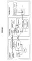
- FIG. 5A through FIG. 5C are block diagrams illustrating the example of the processing paths during the parallel processing.
- the processing path of the output image display procedure indicated by solid lines changes depending on the progress of the output image display procedure in the time period from FIG. 3A to FIG. 3I.
- FIG. 7A through FIG. 7I show the magnitude of the processing workload on the controller chip 121, the CPU 123, and the memory 124 at corresponding times.
- the CPU 132 uses the image processing chip 134 to produce the output image of the image files stored in the memory 131, and to display the output image on the liquid crystal monitor 133 for confirmation of the user.
- a fourth processing performed by the image processing chip 134 is to display the output image of image files received by the network 127 on the liquid crystal monitor 133.
- the information processing device 100 includes the engine unit 110, the controller unit 120, and the operational unit 130.
- the CPU interface (I/F) 820 is an interface between the controller chip 121 and the CPU 123 of the controller unit 120.
- FIG. 11 is a block diagram illustrating a functional configuration of the image processing chip 134 according to the present embodiment of the present invention.
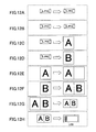
- FIG. 12A through FIG. 12H are diagrams illustrating the output image display procedure according to the present embodiment of the present invention.
- FIG. 12E and FIG. 12F illustrate an operation of combining two decomposed image files and producing the output image.
- the processing paths of the output image display procedure at this stage as illustrated by solid lines in FIG. 14B and FIG. 14C, pass through the memory 131 and the CPU 132 of the operational unit 130.
- FIG. 17 is a block diagram illustrating a hardware configuration of an information processing device according to another embodiment of the present invention.
- the processing workload is not concentrated on the controller chip 121 but is appropriately distributed.
- FIG. 18 corresponds to FIG. 15A in the previous embodiment, and the processing paths at other timings in the present embodiment are the same as those shown in FIG. 13A through FIG. 13C, FIG. 14A through FIG. 14C, and FIG. 15B except that the image processing chip 134 is absent.
Landscapes
- Engineering & Computer Science (AREA)
- Multimedia (AREA)
- Signal Processing (AREA)
- Computer Hardware Design (AREA)
- Microelectronics & Electronic Packaging (AREA)
- Human Computer Interaction (AREA)
- General Engineering & Computer Science (AREA)
- Facsimiles In General (AREA)
- Image Processing (AREA)
- Record Information Processing For Printing (AREA)
- Digital Computer Display Output (AREA)
Abstract
Description
- The present invention relates to an information processing device, an information processing method, and an information processing system, and particularly, to an information processing device, an information processing method, and an information processing system that displays an output image of image files on a display device for confirmation by a user.
- In recent years and continuing, a multi-function peripheral (MFP), which is an information processing device, is developed to have more and more functions. For example, the multi-function peripheral is capable of image combination, scaling (reduction and enlargement) of image size, image rotation, color conversion, stamping, and other various kinds of processing on the image files. An operator of the multi-function peripheral can combine various kinds of processing on the image file. However, when combining various kinds of processing on the image file, it is not easy for the operator to imagine the output image produced after the various kinds of processing.
- To solve this problem, in the related art, for example,
Japanese Laid-Open Patent Application No. 2003-51907 - Since the multi-function peripheral has plural functions of a printer, a scanner, a facsimile machine, and others, and it is thus able to perform processing of displaying output images, scanner inputting processing, rotation processing, and other processing in parallel. For this reason, the multi-function peripheral is liable to concentrate processing on the CPU of a controller unit, which performs overall control of the multi-function peripheral.
- In addition, among the processing performed by the CPU of the controller unit, the image processing is one of the processing operations having a large workload. Thus, in the multi-function peripheral, a CPU and a controller chip are provided in the controller unit, and the controller chip assumes the image processing originally assigned to the CPU of the controller unit to distribute the workload.
- However, since the image processing has a large workload, when the controller chip assumes the image processing originally assigned to the CPU, the processing is concentrated on the controller chip.
- Furthermore, when producing the output image after processing and outputting the output image for confirmation by the operator, one would rather produce the output image with the real image of the image files to be processed than use the output image prepared in advance.
- However, the workload of the image processing of producing the output image with the real image increases noticeably; thus, the processing is much concentrated on the controller chip. Since the controller unit performs overall control of the multi-function peripheral, it is not preferable that the processing be concentrated on the CPU of the controller chip and the controller chip of the controller unit.
- An embodiment of the present invention may solve one or more problems of the related art.
- A preferred embodiment of the present invention may provide an information processing device, an information processing method, and an information processing system able to distribute a processing workload, and allowing easy confirmation of an output image of processed images.
- According to a first aspect of the present invention, there is provided an information processing device, comprising:
- an engine unit that performs image forming processing;
- a controller unit that controls overall operations of the information processing device; and
- an operational unit that serves as a user interface,
- According to a second aspect of the present invention, there is provided an information processing method of an information processing device including an engine unit that performs image forming processing; a controller unit that controls overall operations of the information processing device; an operational unit that serves as a user interface, wherein the controller unit includes a first memory for storing one or more image files to be transmitted to the operational unit, a first calculation and processing unit that controls overall operations of the information processing device, and a first image processing unit that assumes part of image processing originally assigned to the first calculation and processing unit,
said method comprising: - a step of producing an output image of the image files after processing in a unit different from the controller unit; and
- a step of displaying the output image on a display device of the operational unit.
- According to a third aspect of the present invention, there is provided an information processing system, comprising:
- an engine unit that performs image forming processing;
- a controller unit that controls overall operations of the information processing system;
- an operational unit that serves as a user interface,
- a first memory for storing one or more image files to be transmitted to the operational unit,
- a first calculation and processing unit that controls overall operations of the information processing system, and
- a first image processing unit that assumes part of image processing originally assigned to the first calculation and processing unit, wherein
- an output image of the image files after processing is produced in a unit different from the controller unit, and the output image is displayed on a display device of the operational unit.
- According to an embodiment of the present invention, it is possible to provide an information processing device, an information processing method, and an information processing system able to distribute a processing workload, and allow an operator to easily imagine an output image of input image files after processing.
- These and other objects, features, and advantages of the present invention will become more apparent from the following detailed description of preferred embodiments given with reference to the accompanying drawings, in which:
- FIG. 1 is a block diagram illustrating a general hardware configuration of an information processing device;
- FIG. 2 is a block diagram illustrating a general software configuration of an information processing device;
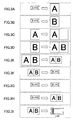
- FIG. 3A through FIG. 3I are diagrams illustrating the output image display procedure;
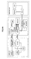
- FIG. 4A through FIG. 4C are block diagrams illustrating an example of plural processing paths during parallel processing;
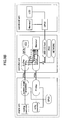
- FIG. 5A through FIG. 5C, continuing from FIG. 4C, are block diagrams illustrating the example of the processing paths during the parallel processing;
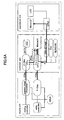
- FIG. 6A through FIG. 6C, continuing from FIG. 5C, are block diagrams illustrating the example of the processing paths during the parallel processing;
- FIG. 7A through FIG. 7I are diagrams illustrating changes with time of workloads on the CPU, the memory and the controller chip;
- FIG. 8 is a block diagram illustrating a hardware configuration of an information processing device according to an embodiment of the present invention;
- FIG. 9 is a block diagram illustrating an example of a software configuration the information processing device according to the present embodiment of the present invention;
- FIG. 10 is a block diagram illustrating a functional configuration the
controller chip 121 according to the present embodiment of the present invention; - FIG. 11 is a block diagram illustrating a functional configuration of the
image processing chip 134 according to the present embodiment of the present invention; - FIG. 12A through FIG. 12H are diagrams illustrating the output image display procedure according to the present embodiment of the present invention;
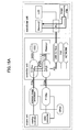
- FIG. 13A through FIG. 13C are block diagrams illustrating an example of plural processing paths during parallel processing in the present embodiment;
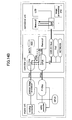
- FIG. 14A through FIG. 14C, continuing from FIG. 13C, are block diagrams illustrating the example of the processing paths during the parallel processing in the present embodiment;
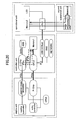
- FIG. 15A and FIG. 15B, continuing from FIG. 14C, are block diagrams illustrating the example of the processing paths during the parallel processing in the present embodiment;
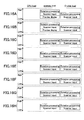
- FIG. 16A through FIG. 16H are diagrams illustrating changes with time of workloads on the CPU, the memory and the controller chip in the present embodiment;
- FIG. 17 is a block diagram illustrating a hardware configuration of an information processing device according to another embodiment of the present invention;
- FIG. 18 is a block diagrams illustrating an example of processing paths during the parallel processing in the present embodiment, in which the
CPU 132 uses software to produce the output image and display the output image on theliquid crystal monitor 133; - FIG. 19 is a block diagram illustrating a hardware configuration of an information processing device according to still another embodiment of the present invention; and
- FIG. 20 is a block diagrams illustrating an example of processing paths during parallel processing in the present embodiment, in which the
image processing chip 141 is used to produce the output image and display the output image on theliquid crystal monitor 133. - Below, preferred embodiments of the present invention are explained with reference to the accompanying drawings.
- First, for easy understanding of the present invention, a general configuration of the information processing device is described first.
- FIG. 1 is a block diagram illustrating a general hardware configuration of an information processing device.
- As shown in FIG. 1, an
information processing device 100 includes anengine unit 110, acontroller unit 120, and anoperational unit 130. - The
engine unit 110 realizes image forming functions of theinformation processing device 100. - The
controller unit 120 performs overall control of theinformation processing device 100. - The
operational unit 130 is a user interface for receiving data from a user through input operations of the user, and providing information for the user. - The
engine unit 110 includes areading controller 111, ascanner image processor 112, awrite controller 113, a plotter chip (P-chip) 114, and aCPU 115. - The
controller unit 120 includes a controller chip (C-chip) 121, a hard-disk drive (HDD) 122, aCPU 123, and amemory 124. - The
operational unit 130 includes amemory 131, aCPU 132, and a liquid crystal monitor (LCD) 133. - The
controller chip 121 and theCPU 123 of thecontroller unit 120 are connected via a PCI express bus (indicated as "PCIe" in FIG. 1). Thecontroller chip 121 assumes the image processing originally assigned to theCPU 123 to distribute the workload. - The
controller chip 121 is connected to thescanner image processor 112 of theengine unit 110 via the PCIe, and is connected to theHDD 122 via a serial ATA (SATA) bus. - The
CPU 123 is connected to theplotter chip 114 of theengine unit 110 via the PCIe, and is connected to thememory 124. In addition, theCPU 123 is connected to a USB 2.0host 125 via a PCI bus. The USB 2.0host 125 is connected to theCPU 132 of theoperational unit 130. Further, theCPU 123 is connected to a facsimile machine (indicated as "FAX" in FIG. 1) 126 and a network (indicated as "NETWORK" in FIG. 1) via the PCI. - In the
information processing device 100 shown in FIG. 1, thecontroller chip 121 is used to perform image combination, scaling (reduction and enlargement) of image size, image rotation, color conversion, stamping, and other various kinds of processing on the image files. Further, theinformation processing device 100 uses thecontroller chip 121 to produce an output image of the original image files, and displays the output image on the liquid crystal monitor (LCD) 133 for confirmation of the user. - Below, descriptions are made of various processing by using the
controller chip 121. - A first processing performed by the
controller chip 121 is to display the output image of image files read from a scanner on theliquid crystal monitor 133. Namely, thecontroller chip 121 displays a preview image for previewing the output image after various processing is performed. - The image files read from the scanner are stored in the
memory 124 of thecontroller unit 120 via thereading controller 111 and thescanner image processor 112 of theengine unit 110, thecontroller chip 121, and theCPU 123 of thecontroller unit 120. TheCPU 123 uses thecontroller chip 121 to produce the output image of the image files stored in thememory 124, and to display the output image on the liquid crystal monitor 133 for confirmation of the user. - A second processing performed by the
controller chip 121 is to display the output image of image files read from thehard disk drive 122 on theliquid crystal monitor 133. - The image files read from the
hard disk drive 122 are stored in thememory 124 of thecontroller unit 120 via thecontroller chip 121 and theCPU 123 of thecontroller unit 120. TheCPU 123 uses thecontroller chip 121 to produce the output image of the image files stored in thememory 124, and to display the output image on the liquid crystal monitor 133 for confirmation of the user. - A third processing performed by the
controller chip 121 is to display the output image of image files received by the facsimile machine (FAX) 126 on theliquid crystal monitor 133. - The image files received by the
facsimile machine 126 are stored in thememory 124 of thecontroller unit 120 via theCPU 123 of thecontroller unit 120. TheCPU 123 uses thecontroller chip 121 to produce the output image of the image files stored in thememory 124, and to display the output image on the liquid crystal monitor 133 for confirmation of the user. - A fourth processing performed by the
controller chip 121 is to display the output image of image files received by thenetwork 127 on theliquid crystal monitor 133. - The image files read from the
network 127 are stored in thememory 124 of thecontroller unit 120 via theCPU 123 of thecontroller unit 120. TheCPU 123 uses thecontroller chip 121 to produce the output image of the image files stored in thememory 124, and to display the output image on the liquid crystal monitor 133 for confirmation of the user. - A fifth processing performed by the
controller chip 121 is to store the image files read from the scanner in thememory 124. - The image files read from the scanner are stored in the
memory 124 of thecontroller unit 120 via thereading controller 111 and thescanner image processor 112 of theengine unit 110, thecontroller chip 121, and theCPU 123 of thecontroller unit 120. - A sixth processing performed by the
controller chip 121 is to output the image files stored in thememory 124 to a plotter. Here, assume the image files stored in thememory 124 are of a RGB format. TheCPU 123 uses thecontroller chip 121 to perform color conversion on the image files stored in thememory 124 from the RGB format to a CMYK format. The thus obtained image files of the CMYK format are output to the plotter via theCPU 123 of thecontroller unit 120, theplotter chip 114 and thewrite controller 113 of the readingcontroller 111, and are output by the plotter. - A seventh processing performed by the
controller chip 121 is to transmit the image files stored in thememory 124 by thefacsimile machine 126. Here, assume the image files stored in thememory 124 are of the RGB format. TheCPU 123 uses thecontroller chip 121 to perform color conversion on the image files stored in thememory 124 from the RGB format to a format compatible with thefacsimile machine 126, such as, a B/W format. The thus obtained image files of the FAX format are transmitted by thefacsimile machine 126 via theCPU 123 of thecontroller unit 120. - An eighth processing performed by the
controller chip 121 is to transmit the image files stored in thememory 124 to thenetwork 127. TheCPU 123 uses thecontroller chip 121 to perform appropriate image processing on the image files stored in thememory 124, and the thus obtained image files are transmitted to thenetwork 127 via theCPU 123 of thecontroller unit 120. - The above first to eighth processing is just exemplified for illustration; it is apparent that the
controller chip 121 can perform other kinds of processing. - In order to perform the above mentioned processing, the
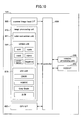
information processing device 100 shown in FIG. 1 may have a software configuration as shown in FIG. 2. - FIG. 2 is a block diagram illustrating a general software configuration of an information processing device.
- As shown in FIG. 2, the
information processing device 100 includes theengine unit 110, thecontroller unit 120, and theoperational unit 130. - The
engine unit 110 of theinformation processing device 100 includes areading control section 211, aprinting control section 212, an enginestatus control section 213, and acommunication control section 214. - The
controller unit 120 includes ajob management section 221, an image formingcontrol section 222, a systemstatus control section 223, an outputimage processing section 224, and acommunication control section 225. - The
operational unit 130 includes adisplay control section 231, and acommunication control section 232. - The software configuration as shown in FIG. 2 is realized by using the hardware configuration as shown in FIG. 1. As shown in FIG. 2, the
controller unit 120 includes the outputimage processing section 224; hence, when displaying the output image on theliquid crystal monitor 133, the outputimage processing section 224 of thecontroller unit 120 produces the output image of the processed image files, and the output image is sent to theoperational unit 130 to display the output image on the liquid crystal monitor 133 of theoperational unit 130. - The various processing performed by the
controller chip 121 is usually performed in parallel. In this case, in theinformation processing device 100 as shown in FIG. 1 and FIG. 2, the processing workload is concentrated on thecontroller chip 121. - Below, descriptions are made of workload concentration on the
controller chip 121 when an output image display procedure, a scanner input procedure, and a rotation procedure are executed in parallel. - FIG. 3A through FIG. 3I are diagrams illustrating the output image display procedure.
- FIG. 3A through FIG. 3I are arranged in temporal sequence. Namely, FIG. 3A corresponds to operations at the earliest time, and FIG. 3I corresponds to operations at the latest time. In addition, in FIG. 3A through FIG. 3I, in the image combination processing, two images are combined into one image (simply indicated as "2 in 1"). Namely, when displaying an output image resulting from a "2 in 1" combination, an output image after two images are combined into one image is displayed.
- FIG. 4A through FIG. 4C are block diagrams illustrating an example of plural processing paths during parallel processing.
- FIG. 5A through FIG. 5C, continuing from FIG. 4C, are block diagrams illustrating the example of the processing paths during the parallel processing.
- FIG. 6A through FIG. 6C, continuing from FIG. 5C, are block diagrams illustrating the example of the processing paths during the parallel processing.
- In FIG. 4A through FIG. 4C, FIG. 5A through FIG. 5C, and FIG. 6A through FIG. 6C, the processing path of the scanner input procedure is indicated by dotted lines, the processing path of the rotation procedure is indicated by dashed lines, and the processing path of the output image display procedure is indicated by solid lines.
- The processing path of the scanner input procedure indicated by dotted lines successively passes through the reading
controller 111 and thescanner image processor 112 of theengine unit 110, and thecontroller chip 121, theCPU 123, and thememory 124 of thecontroller unit 120 in the time period from FIG. 3A to FIG. 3I. - The processing path of the rotation procedure indicated by dashed lines successively passes through the
controller chip 121, theCPU 123, and thememory 124 of thecontroller unit 120 in the time period from FIG. 3A to FIG. 3I. - The processing path of the output image display procedure indicated by solid lines changes depending on the progress of the output image display procedure in the time period from FIG. 3A to FIG. 3I.
- Next, the output image display procedure is explained with reference to FIG. 3A through FIG. 3I, FIG. 4A through FIG. 4C, FIG. 5A through FIG. 5C, and FIG. 6A through FIG. 6C.
- FIG. 3A and FIG. 3B illustrate an operation of decomposing JPEG compressed image files. The processing paths of the output image display procedure at this stage, as illustrated by solid lines in FIG. 4A and FIG. 4B, pass through the
CPU 123, and thememory 124 of thecontroller unit 120. - FIG. 3C and FIG. 3D illustrate an operation of combining two decomposed image files and producing the output image. The processing paths of the output image display procedure at this stage, as illustrated by solid lines in FIG. 4C and FIG. 5A, pass through the
CPU 123, and thememory 124 of thecontroller unit 120. - FIG. 3E illustrates an operation of reducing the size of the combined image file. The processing path of the output image display procedure at this stage, as illustrated by solid lines in FIG. 5B, passes through the
controller chip 121, theCPU 123, and thememory 124 of thecontroller unit 120. - FIG. 3F illustrates an operation of compressing the reduced image file. The processing path of the output image display procedure at this stage, as illustrated by solid lines in FIG. 5C, passes through the
controller chip 121, theCPU 123, and thememory 124 of thecontroller unit 120. - FIG. 3G illustrates an operation of sending the compressed image file to the
memory 131 of theoperational unit 130. The processing path of the output image display procedure at this stage, as illustrated by solid lines in FIG. 6A, passes through thememory 131 and theCPU 132 of theoperational unit 130. - FIG. 3H illustrates an operation of decompressing the compressed JPEG image file. The processing path of the output image display procedure at this stage, as illustrated by solid lines in FIG. 6B, passes through the
memory 131 and theCPU 132 of theoperational unit 130. - FIG. 3I illustrates an operation of displaying the decompressed image file on the liquid crystal monitor (LCD) 133 of the
operational unit 130. The processing path of the output image display procedure at this stage, as illustrated by solid lines in FIG. 6C, passes through thememory 131, theCPU 132, and the liquid crystal monitor (LCD) 133 of theoperational unit 130. - FIG. 7A through FIG. 7I are diagrams illustrating changes with time of workloads on the CPU, the memory and the controller chip.
- Specifically, FIG. 7A through FIG. 7I show the magnitude of the processing workload on the
controller chip 121, theCPU 123, and thememory 124 at corresponding times. - Similar to FIG. 3A through FIG. 3I, FIG. 7A through FIG. 7I are also arranged in temporal sequence, namely, FIG. 7A corresponds to operations at the earliest time, FIG. 7I corresponds to operations at the latest time, and FIG. 7A through FIG. 7I are associated with image combination processing, in which two images are combined into one image (namely, "2 in 1" combination).
- As shown in FIG. 7A through FIG. 7I, when the output image display procedure, the scanner input procedure, and the rotation procedure are executed in parallel, the processing workloads are concentrated on the
controller chip 121 and thememory 124. - As described above with reference to FIG. 3A through FIG. 3I, FIG. 4A through FIG. 4C, FIG. 5A through FIG. 5C, FIG. 6A through FIG. 6C, and FIG. 7A through FIG. 7I, the
information processing device 100 shown in FIG. 1 is a controller-centralized device, in which the output image is produced in thecontroller unit 120. The output image may be produced in the operational unit 130 (this is the so-called "operational unit-centralized device"). Further, production of the output image may also be performed in any components of theinformation processing device 100 other than thecontroller unit 120. In this case, the operations of thecontroller unit 120 of the controller-centralizedinformation processing device 100 should be shifted to components of theinformation processing device 100 other than thecontroller unit 120. - In order to produce the output image in components of the
information processing device 100 other than thecontroller unit 120, for example, it can be attempted to provide an image processing chip or a software package equivalent to the image processing unit of thecontroller chip 121 in the component of theinformation processing device 100 which is different from thecontroller unit 120. Alternatively, it can be attempted to provide plural image processing units of thecontroller chip 121 of thecontroller unit 120. However, from the point of view of data buses and the number of sequence steps, it is efficient to provide an image processing chip or a software package equivalent to the image processing unit of thecontroller chip 121 in components different from thecontroller unit 120 compared to providing plural image processing units of thecontroller chip 121 of thecontroller unit 120. - Below, descriptions are made of an information processing device in which an image processing chip or a software package equivalent to the image processing unit of the
controller chip 121 is provided in components different from thecontroller unit 120. - FIG. 8 is a block diagram illustrating a hardware configuration of an information processing device according to an embodiment of the present invention.
- An
information processing device 100 shown in FIG. 8 is basically the same as theinformation processing device 100 shown in FIG. 1 except that animage processing chip 134, which is the same as the image processing chip in the controller chip (C-chip) 121, is additionally provided in theoperational unit 130. Below, the same reference numbers are assigned to the same components as those described previously, and overlapping descriptions are omitted. - In the
information processing device 100 shown in FIG. 8, theoperational unit 130 includes thememory 131, theCPU 132, the liquid crystal monitor (LCD) 133, and theimage processing chip 134. - The
CPU 132 is connected to the USB 2.0host 125 of thecontroller unit 120, and is connected to thememory 131, the liquid crystal monitor (LCD) 133, and theimage processing chip 134 of theoperational unit 130. - In the
information processing device 100 shown in FIG. 8, theimage processing chip 134 is used to perform image combination, scaling (reduction and enlargement) of image size, image rotation, color conversion, stamping, and other various kinds of processing on the image files, the same as the image processing unit of thecontroller chip 121. Further, theinformation processing device 100 uses theimage processing chip 134 to produce the output image of the original image files, and displays the output image on the liquid crystal monitor 133 for confirmation of the user. - Below, descriptions are made of various processing by using the
image processing chip 134. - A first processing performed by the
image processing chip 134 is to display the output image of image files read from the scanner on theliquid crystal monitor 133. - The image files read from the scanner are stored in the
memory 124 of thecontroller unit 120 via thereading controller 111 and thescanner image processor 112 of theengine unit 110, thecontroller chip 121, and theCPU 123 of thecontroller unit 120; the image files stored in thememory 124 are transmitted and stored in thememory 131 through theCPU 123 and the USB 2.0host 125 of thecontroller unit 120, and theCPU 132 of theoperational unit 130. - The
CPU 132 uses theimage processing chip 134 to produce the output image of the image files stored in thememory 131, and to display the output image on the liquid crystal monitor 133 for confirmation of the user. - A second processing performed by the
image processing chip 134 is to display the output image of image files read from thehard disk drive 122 on theliquid crystal monitor 133. - The image files read from the
hard disk drive 122 are stored in thememory 124 of thecontroller unit 120 via thecontroller chip 121 and theCPU 123 of thecontroller unit 120; the image files stored in thememory 124 are transmitted and stored in thememory 131 through theCPU 123 and the USB 2.0host 125 of thecontroller unit 120, and theCPU 132 of theoperational unit 130. - The
CPU 132 uses theimage processing chip 134 to produce the output image of the image files stored in thememory 131, and to display the output image on the liquid crystal monitor 133 for confirmation of the user. - A third processing performed by the
image processing chip 134 is to display the output image of image files received by the facsimile machine (FAX) 126 on theliquid crystal monitor 133. - The image files received by the
facsimile machine 126 are stored in thememory 124 of thecontroller unit 120 via theCPU 123 of thecontroller unit 120; the image files stored in thememory 124 are transmitted and stored in thememory 131 through theCPU 123 and the USB 2.0host 125 of thecontroller unit 120, and theCPU 132 of theoperational unit 130. - The
CPU 132 uses theimage processing chip 134 to produce the output image of the image files stored in thememory 131, and to display the output image on the liquid crystal monitor 133 for confirmation of the user. - A fourth processing performed by the
image processing chip 134 is to display the output image of image files received by thenetwork 127 on theliquid crystal monitor 133. - The image files received by the
network 127 are stored in thememory 124 of thecontroller unit 120 via theCPU 123 of thecontroller unit 120; the image files stored in thememory 124 are transmitted and stored in thememory 131 through theCPU 123 and the USB 2.0host 125 of thecontroller unit 120, and theCPU 132 of theoperational unit 130. - The
CPU 132 uses theimage processing chip 134 to produce the output image of the image files stored in thememory 131, and to display the output image on the liquid crystal monitor 133 for confirmation of the user. - As described above, in the
information processing device 100 shown in FIG. 8, among the aforementioned first to eighth processing operations performed by using thecontroller chip 121, the first through the fourth processing operations are performed in theimage processing chip 134 of theoperational unit 130. - In order to perform the above mentioned processing, the
information processing device 100 shown in FIG. 8 may have a software configuration as shown in FIG. 9. - FIG. 9 is a block diagram illustrating an example of a software configuration the information processing device according to the present embodiment of the present invention.
- The
information processing device 100 shown in FIG. 9 is basically the same as theinformation processing device 100 shown in FIG. 2 except that the outputimage processing section 224 in thecontroller unit 120 of theinformation processing device 100 in FIG. 2 is omitted and an outputimage processing section 233 is provided in theoperational unit 130 of theinformation processing device 100 shown in FIG. 8. Below, the same reference numbers are assigned to the same components as those described previously, and overlapping descriptions are omitted. - As shown in FIG. 9, the
information processing device 100 includes theengine unit 110, thecontroller unit 120, and theoperational unit 130. - The
engine unit 110 of theinformation processing device 100 includes areading control section 211, aprinting control section 212, an enginestatus control section 213, and acommunication control section 214. - The
controller unit 120 includes ajob management section 221, an image formingcontrol section 222, a systemstatus control section 223, and acommunication control section 225. - The
operational unit 130 includes adisplay control section 231, acommunication control section 232, and an outputimage processing section 233. - The software configuration as shown in FIG. 9 is realized by using the hardware configuration as shown in FIG. 8. As shown in FIG. 9, the
operational unit 130 includes the outputimage processing section 233; hence, when displaying the output image on theliquid crystal monitor 133, the image files are transmitted from thecontroller unit 120 to theoperational unit 130, the outputimage processing section 233 of theoperational unit 130 produces the output image of the processed image files, and the output image is displayed on the liquid crystal monitor 133 of theoperational unit 130. - Therefore, in the
information processing device 100 shown in FIG. 8 and FIG. 9, among various procedures executed by thecontroller chip 121 in theinformation processing device 100 shown in FIG. 1 and FIG. 2, the output image display procedure is executed by theimage processing chip 134 of theoperational unit 130; hence, the processing workload is distributed in theinformation processing device 100 shown in FIG. 8 and FIG. 9 compared to theinformation processing device 100 shown in FIG. 1 and FIG. 2. - Below, descriptions are made of the
controller chip 121 and theimage processing chip 134 according to the present embodiment of the present invention. - FIG. 10 is a block diagram illustrating a functional configuration the
controller chip 121 according to the present embodiment of the present invention. - As shown in FIG. 10, the
controller chip 121 includes a scanner image input interface (I/F) 800, animage processing unit 810, a CPU interface (I/F) 820, acontroller 830, arotation processing unit 840, and a HDD interface (I/F) 850. - The scanner image input interface (I/F) 800 is the interface between the
controller chip 121 and thescanner image processor 112 of theengine unit 110. - The
image processing unit 810 includes acolor conversion unit 811, anedition unit 812, and aplot unit 813. - The
color conversion unit 811 performs color conversion of an image file. Theedition unit 812 performs editing of the image file. Theplot unit 813 performs plotting of the image file. - The CPU interface (I/F) 820 is an interface between the
controller chip 121 and theCPU 123 of thecontroller unit 120. - The
controller 830 controls the scanner image input interface (I/F) 800, theimage processing unit 810, the CPU interface (I/F) 820, acontroller 830, therotation processing unit 840, and the HDD interface (I/F) 850. - The
rotation processing unit 840 performs rotation processing. The HDD interface (I/F) 850 is an interface between thecontroller chip 121 and the hard-disk drive (HDD) 122. - FIG. 11 is a block diagram illustrating a functional configuration of the
image processing chip 134 according to the present embodiment of the present invention. - As shown in FIG. 11, the
image processing chip 134 includes a CPU interface (I/F) 900, acontroller 910, animage processing unit 920, and arotation processing unit 930. - The CPU interface (I/F) 900 is an interface between the
image processing chip 134 and theCPU 132 of theoperational unit 130. - The
controller 910 controls the CPU interface (I/F) 900, theimage processing unit 920, and therotation processing unit 930. - The
image processing unit 920 includes acolor conversion unit 921 and anedition unit 922. - The
color conversion unit 921 performs color conversion of an image file. Theedition unit 922 performs editing of the image file. - The
rotation processing unit 930 performs rotation processing. - The
image processing chip 134 shown in FIG. 11 has the same image processing functions of producing an output image of an input image as thecontroller chip 121 shown in FIG. 10. Specifically, similar to thecontroller chip 121 shown in FIG. 10, theimage processing chip 134 shown in FIG. 11 also has theimage processing unit 920 and therotation processing unit 930. - The
image processing unit 920 includes acolor conversion unit 921 and anedition unit 922, which correspond to thecolor conversion unit 811 and theedition unit 812 of theimage processing unit 810, respectively. Similar to theedition unit 812 of theimage processing unit 810, theedition unit 922 has the shift function, mask function, scaling function, mirror function, negative function, and others. - With the above configuration, the
image processing chip 134 has the same image processing functions of producing an output image of an input image as thecontroller chip 121. - With the
information processing device 100 shown in FIG. 8, when the output image display procedure, the scanner input procedure, and the rotation procedure are executed in parallel, the processing workload is not concentrated on thecontroller chip 121 but is appropriately distributed. - FIG. 12A through FIG. 12H are diagrams illustrating the output image display procedure according to the present embodiment of the present invention.
- FIG. 12A through FIG. 12H are arranged in temporal sequence. Namely, FIG. 12A corresponds to operations at the earliest time, and FIG. 12H corresponds to operations at the latest time. In addition, in FIG. 12A through FIG. 12H, in the image combination processing, two images are combined into one image (simply indicated as "2 in 1"). Namely, when displaying an output image of the "2 in 1" combination processing, an output image after two images are combined into one image is displayed.
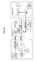
- FIG. 13A through FIG. 13C are block diagrams illustrating an example of plural processing paths during parallel processing in the present embodiment.
- FIG. 14A through FIG. 14C, continuing from FIG. 13C, are block diagrams illustrating the example of the processing paths during the parallel processing in the present embodiment.
- FIG. 15A and FIG. 15B, continuing from FIG. 14C, are block diagrams illustrating the example of the processing paths during the parallel processing in the present embodiment.
- In FIG. 13A through FIG. 13C, FIG. 14A through FIG. 14C, and FIG. 15A through FIG. 15B, the processing path of the scanner input procedure is indicated by dotted lines, the processing path of the rotation procedure is indicated by dashed lines, and the processing path of the output image display procedure is indicated by solid lines.
- The processing path of the scanner input procedure indicated by the dotted lines successively passes through the reading
controller 111 and thescanner image processor 112 of theengine unit 110, and thecontroller chip 121, theCPU 123, and thememory 124 of thecontroller unit 120 in the time period from FIG. 12A to FIG. 12H. - The processing path of the rotation procedure indicated by dashed lines successively passes through the
controller chip 121, theCPU 123, and thememory 124 of thecontroller unit 120 in the time period from FIG. 12A to FIG. 12H. - The processing path of the output image display procedure indicated by solid lines changes depending on the progress of the output image display procedure in the time period from FIG. 12A to FIG. 12H.
- Next, the output image display procedure is explained with reference to FIG. 12A through FIG. 12H, FIG. 13A through FIG. 13C, FIG. 14A through FIG. 14C, and FIG. 15A and FIG. 15B.
- FIG. 12A and FIG. 12B illustrate an operation of sending a compressed JPEG image file from the
memory 124 of thecontroller unit 120 to thememory 131 of theoperational unit 130. The processing paths of the output image display procedure at this stage, as illustrated by solid lines in FIG. 13A and FIG. 13B, pass through theCPU 123 and thememory 124 of thecontroller unit 120, and thememory 131 and theCPU 132 of theoperational unit 130. - FIG. 12C and FIG. 12D illustrate an operation of decomposing the JPEG compressed image files. The processing paths of the output image display procedure at this stage, as illustrated by solid lines in FIG. 13C and FIG. 13D, pass through the
memory 131 and theCPU 132 of theoperational unit 130. - FIG. 12E and FIG. 12F illustrate an operation of combining two decomposed image files and producing the output image. The processing paths of the output image display procedure at this stage, as illustrated by solid lines in FIG. 14B and FIG. 14C, pass through the
memory 131 and theCPU 132 of theoperational unit 130. - FIG. 12G illustrates an operation of reducing the size of the combined image file. The processing path of the output image display procedure at this stage, as illustrated by solid lines in FIG. 15A, passes through the
memory 131, theCPU 132, theimage processing chip 134 of theoperational unit 130. - FIG. 12H illustrates an operation of displaying the reduced image file on the liquid crystal monitor (LCD) 133 of the
operational unit 130. The processing path of the output image display procedure at this stage, as illustrated by solid lines in FIG. 15B, passes through thememory 131, theCPU 132, and the liquid crystal monitor (LCD) 133 of theoperational unit 130. - FIG. 16A through FIG. 16H are diagrams illustrating changes with time of workloads on the CPU, the memory and the controller chip in the present embodiment.
- Specifically, FIG. 16A through FIG. 16H show the magnitude of the processing workload on the
controller chip 121, theCPU 123, and thememory 124 at corresponding time. - Similar to FIG. 12A through FIG. 12H, FIG. 16A through FIG. 16H are also arranged in temporal sequence, namely, FIG. 16A corresponds to operations at the earliest time, and FIG. 16H corresponds to operations at the latest time, and FIG. 16A through FIG. 16H are associated with an image combination processing, in which two images are combined into one image (namely, "2 in 1" combination).
- As shown in FIG. 16A through FIG. 16H, when the output image display procedure, the scanner input procedure, and the rotation procedure are executed in parallel, the processing workloads are not concentrated on the
controller chip 121 and thememory 124, but are appropriately distributed. - As described above with reference to FIG. 12A through FIG. 12H, FIG. 13A through FIG. 13C, FIG. 14A through FIG. 14C, FIG. 15A and FIG. 15B, and FIG. 16A through FIG. 16H, the
information processing device 100 shown in FIG. 8 is an operational unit-centralized device, in which the output image is produced in theoperational unit 130. In theinformation processing device 100 shown in FIG. 8, the image display processing originally performed by thecontroller chip 121 in the controller-centralizedinformation processing device 100 is performed by theimage processing chip 134 of theoperational unit 130; thereby, even though the image display processing is of a high workload, the workload on thecontroller chip 121 is low. Therefore, with theinformation processing device 100 shown in FIG. 8, it is possible to easily perform the image display processing having a high workload. - FIG. 17 is a block diagram illustrating a hardware configuration of an information processing device according to another embodiment of the present invention.
- An
information processing device 100 shown in FIG. 17 is basically the same as theinformation processing device 100 shown in FIG. 8 except that operations of theimage processing unit 810 in thecontroller chip 121 are performed by theCPU 132 of theoperational unit 130 with software; therefore theimage processing chip 134 is not provided in theoperational unit 130. Below, the same reference numbers are assigned to the same components as those described previously, and overlapping descriptions are omitted. - In the
information processing device 100 shown in FIG. 17, theCPU 132 uses software to perform image combination, scaling (reduction and enlargement) of image size, image rotation, color conversion, stamping, and other various kinds of processing on the image files, the same as the image processing unit of thecontroller chip 121. Further, theinformation processing device 100 uses theCPU 132 to produce the output image of the original image files by using the software, and displays the output image on the liquid crystal monitor 133 for confirmation of the user. - With the
information processing device 100 shown in FIG. 17, when the output image display procedure, the scanner input procedure, and the rotation procedure are executed in parallel, the processing workload is not concentrated on thecontroller chip 121 but is appropriately distributed. - The output image display procedure in the present embodiment is the same as that shown in FIG. 12A through FIG. 12H.
- FIG. 18 is a block diagrams illustrating an example of processing paths during the parallel processing in the present embodiment, in which the
CPU 132 uses software to produce the output image and display the output image on theliquid crystal monitor 133. - Note that FIG. 18 corresponds to FIG. 15A in the previous embodiment, and the processing paths at other timings in the present embodiment are the same as those shown in FIG. 13A through FIG. 13C, FIG. 14A through FIG. 14C, and FIG. 15B except that the
image processing chip 134 is absent. - In an operation of reducing the size of the combined image file, the processing path of the output image display procedure at this stage, as illustrated by solid lines in FIG. 18, passes through the
memory 131, theCPU 132, and theimage processing chip 134 of theoperational unit 130. - As described above, in the
information processing device 100 shown in FIG. 17 and FIG. 18, when the output image display procedure, the scanner input procedure, and the rotation procedure are executed in parallel, the processing workloads are not concentrated on thecontroller chip 121 and thememory 124, but are appropriately distributed. - In the
information processing device 100 shown in FIG. 17 and FIG. 18, the output image is produced by theCPU 132 with software. Since the image display processing originally performed by thecontroller chip 121 in the controller-centralizedinformation processing device 100 is performed by theCPU 132 with software, even though the image display processing is of a high workload, the workload on thecontroller chip 121 is low. Therefore, with theinformation processing device 100 shown in FIG. 17 and FIG. 18, it is possible to easily perform the image display processing having a high workload. - FIG. 19 is a block diagram illustrating a hardware configuration of an information processing device according to still another embodiment of the present invention.
- An
information processing device 100 shown in FIG. 19 is basically the same as theinformation processing device 100 shown in FIG. 1 except that a secondoperational unit 140 is additionally connected to theoperational unit 130. - The second
operational unit 140 includes animage processing chip 141 and amemory 142. Theimage processing chip 141 performs the same image processing as that in thecontroller chip 121. - Below, the same reference numbers are assigned to the same components as those described previously, and overlapping descriptions are omitted.
- In the
information processing device 100 shown in FIG. 19, theimage processing chip 141 is used to perform image combination, scaling (reduction and enlargement) of image size, image rotation, color conversion, stamping, and other various kinds of processing on the image files, the same as the image processing unit of thecontroller chip 121. Further, theinformation processing device 100 uses theimage processing chip 141 to produce the output image of the original image files, and displays the output image on the liquid crystal monitor 133 for confirmation of the user. - With the
information processing device 100 shown in FIG. 19, when the output image display procedure, the scanner input procedure, and the rotation procedure are executed in parallel, the processing workload is not concentrated on thecontroller chip 121 but is appropriately distributed. - The output image display procedure in the present embodiment is the same as that shown in FIG. 12A through FIG. 12H.
- FIG. 20 is a block diagrams illustrating an example of processing paths during parallel processing in the present embodiment, in which the
image processing chip 141 is used to produce the output image and display the output image on theliquid crystal monitor 133. - Note that FIG. 20 corresponds to FIG. 15A in the previous embodiment, and the processing paths at other timings in the present embodiment are the same as those shown in FIG. 13A through FIG. 13C, FIG. 14A through FIG. 14C, and FIG. 15B except that the
image processing chip 134 is absent and the secondoperational unit 140 is present. - In an operation of reducing the size of the combined image file, the processing path of the output image display procedure at this stage, as illustrated by solid lines in FIG. 20, passes through the
memory 131, theCPU 132, theimage processing chip 141 and thememory 142 of the secondoperational unit 140. - In the
information processing device 100 shown in FIG. 19 and FIG. 20, since the secondoperational unit 140 including theimage processing chip 141 and thememory 142 are provided in addition to theoperational unit 130, thememory 131 of theoperational unit 130 can be used as a working memory for displaying images. In addition, theCPU 132 accesses theimage processing chip 141 of the secondoperational unit 140 by register accessing. - As described above, in the
information processing device 100 shown in FIG. 19 and FIG. 20, when the output image display procedure, the scanner input procedure, and the rotation procedure are executed in parallel, the processing workloads are not concentrated on thecontroller chip 121 and thememory 124, but are appropriately distributed. - In the
information processing device 100 shown in FIG. 19 and FIG. 20, the output image is produced by the secondoperational unit 140. Since the image display processing originally performed by thecontroller chip 121 in the controller-centralizedinformation processing device 100 is assumed by the secondoperational unit 140, even though the image display processing is of a high workload, the workload on thecontroller chip 121 is low. Therefore, with theinformation processing device 100 shown in FIG. 19 and FIG. 20, it is possible to easily perform the image display processing having a high workload. - According to the above embodiments, it is possible to produce the output image with the real image of the image files to be processed, and with this output image, it is possible to easily confirm the output image of processed images.
- While the present invention is described with reference to specific embodiments chosen for purpose of illustration, it should be apparent that the invention is not limited to these embodiments, but numerous modifications could be made thereto by those skilled in the art without departing from the basic concept and scope of the invention.
- For example, application of the present invention, or components of the present invention, or combinations of the components of the present invention to methods, devices, systems, computer programs, recording media, and data structures are within the scope of the present invention.
- Further, not only can production of an output image be performed in a unit different from the
controller unit 120, other processing, such as the color conversion processing, or other processing of a high workload, can also be performed in a unit other than thecontroller unit 120. - This patent application is based on
Japanese Priority Patent Applications No. 2006-075647
the controller unit includes
a first memory for storing one or more image files to be transmitted to the operational unit,
a first calculation and processing unit that controls overall operations of the information processing device, and
a first image processing unit that assumes part of image processing originally assigned to the first calculation and processing unit, wherein
an output image of the image files after processing is produced in a unit different from the controller unit, and the output image is displayed on a display device of the operational unit.
the controller unit includes:
Claims (15)
- An information processing device, comprising:an engine unit that performs image forming processing;a controller unit that controls overall operations of the information processing device; andan operational unit that serves as a user interface;wherein
the controller unit includes
a first memory for storing one or more image files to be transmitted to the operational unit,
a first calculation and processing unit that controls overall operations of the information processing device, and
a first image processing unit that assumes part of image processing originally assigned to the first calculation and processing unit, wherein
an output image of the image files after processing is produced in a unit different from the controller unit, and the output image is displayed on a display device of the operation unit. - The information processing device as claimed in claim 1, wherein
the operational unit includes:a second memory that stores the one or more image files transmitted from the controller unit;a second image processing unit that produces the output image of the image files stored in the second memory after the processing on the image files; anda second calculation and processing unit that displays the output image on the display device of the operational unit. - The information processing device as claimed in claim 2, wherein
the second memory stores one or more compressed image files, and
the second image processing unit produces the output image of the image files after processing, said image files being decompressed by the second calculation and processing unit. - The information processing device as claimed in claim 1, wherein
the operation unit includes:a second memory that stores the one or more image files transmitted from the controller unit; anda second calculation and processing unit that produces the output image of the image files stored in the second memory after processing on the image files, and displays the output image on the display device of the operational unit. - The information processing device as claimed in claim 1, wherein
the operation unit includes:a second memory that stores the one or more image files transmitted from the controller unit;a second calculation and processing unit that displays, on the display device of the operational unit, the output image of the image files stored in the second memory after the processing on the image files; anda second image processing unit that produces the output image of the image files stored in the second memory after processing on the image files in a unit different from the engine unit, the controller unit, and the operational unit. - The information processing device as claimed in claim 1, 2, 3, 4 or 5 wherein the processing on the image files resulting in the output image includes at least one of combining the image files, scaling the image files, rotating the image files, and converting colors of the image files.
- The information processing device as claimed in any one of the preceding claims, wherein the first memory stores image files input from a scanner or a facsimile machine, image files read out from a storage device, or image files obtained from a network, said image files being compressed by first memory.
- The information processing device as claimed in claim 7, wherein the first calculation and processing unit and the first image processing unit perform two or more of a process of storing the image files input from the scanner into the first memory, a process of outputting the image files stored in the first memory to a plotter, a process of transmitting the image files stored in the first memory from the facsimile machine, and a process of transmitting the image files stored in the first memory to the network in parallel.
- An information processing method of an information processing device including an engine unit that performs image forming processing; a controller unit that controls overall operations of the information processing device; an operation unit that serves as a user interface, wherein the controller unit includes a first memory for storing one or more image files to be transmitted to the operation unit, a first calculation and processing unit that assumes part of image processing originally assigned to the first calculation and processing unit, said method comprising:a step of producing an output image of the image files after processing in a unit different from the controller unit; anda step of displaying the output image on a display device of the operation unit.
- The information processing method as claimed in claim 9, further comprising:a step of storing the one or more image files transmitted from the controller unit into a second memory in the operation unit;a step of producing the output image of the image files stored in the second memory after processing on the image files; anda step of displaying the output image on the display device of the operation unit.
- The information processing method as claimed in claim 10, further comprising:a step of producing the output image of the image files compressed and stored in the second memory in a second image processing unit in the operational unit, said compressed image files stored in the second memory being decompressed by a second calculation and processing unit in the operational unit.
- The information processing method as claimed in claim 9, further comprising:a step of storing the one or more image files transmitted from the controller unit into a second memory in the operational unit;a step of producing the output image of the image files stored in the second memory after processing on the image files in a unit different from the engine unit, the controller unit, and the operational unit; anda step of displaying the output image of the image files stored in the second memory after processing on the image files on the display device of the operational unit.
- The information processing method as claimed in claim 9, wherein the processing on the image files resulting in the output image includes at least one of combining the image files, scaling the image files, rotating the image files, and converting colors of the image files.
- The information processing method as claimed any one of claims 9 to 13, wherein the first memory compresses and stores image files input from a scanner or a facsimile machine, image files read out from a storage device, or image files obtained from a network.
- The information processing method as claimed in claim 14, wherein the first calculation and processing unit and the first image processing unit perform two or more of a process of storing the image files input from the scanner into the first memory, a process of outputting the image files stored in the first memory to a plotter, a process of transmitting the image files stored in the first memory from the facsimile machine, and a process of transmitting the image files stored in the first memory to the network in parallel.
Applications Claiming Priority (2)
| Application Number | Priority Date | Filing Date | Title |
|---|---|---|---|
| JP2006075641 | 2006-03-17 | ||
| JP2007057883A JP5025290B2 (en) | 2006-03-17 | 2007-03-07 | Image processing apparatus, image processing method, and image processing system |
Publications (3)
| Publication Number | Publication Date |
|---|---|
| EP1835457A2 true EP1835457A2 (en) | 2007-09-19 |
| EP1835457A3 EP1835457A3 (en) | 2008-01-23 |
| EP1835457B1 EP1835457B1 (en) | 2011-11-09 |
Family
ID=38229236
Family Applications (1)
| Application Number | Title | Priority Date | Filing Date |
|---|---|---|---|
| EP07251092A Active EP1835457B1 (en) | 2006-03-17 | 2007-03-15 | Information processing device, information processing method, and information processing system |
Country Status (4)
| Country | Link |
|---|---|
| US (1) | US7843617B2 (en) |
| EP (1) | EP1835457B1 (en) |
| JP (1) | JP5025290B2 (en) |
| CN (1) | CN101101478B (en) |
Families Citing this family (7)
| Publication number | Priority date | Publication date | Assignee | Title |
|---|---|---|---|---|
| JP4752622B2 (en) * | 2006-05-30 | 2011-08-17 | ブラザー工業株式会社 | Image processing apparatus and image processing program |
| JP4855917B2 (en) * | 2006-12-07 | 2012-01-18 | 株式会社リコー | Image forming apparatus, image forming method, and image forming program |
| JP4861255B2 (en) * | 2007-06-14 | 2012-01-25 | 株式会社リコー | Image forming apparatus, image forming method, and program |
| JP5187007B2 (en) * | 2008-06-05 | 2013-04-24 | 株式会社リコー | Image forming apparatus, display control method, and display control program |
| JP5304478B2 (en) | 2008-08-07 | 2013-10-02 | 株式会社リコー | Image forming apparatus, operation screen updating method and program |
| JP5444960B2 (en) * | 2009-09-01 | 2014-03-19 | 株式会社リコー | Information processing apparatus, data migration method, and recording medium |
| JP5358710B2 (en) * | 2012-03-07 | 2013-12-04 | 京セラドキュメントソリューションズ株式会社 | Electronic device and file compression transfer program |
Citations (1)
| Publication number | Priority date | Publication date | Assignee | Title |
|---|---|---|---|---|
| US20030030650A1 (en) | 2001-08-07 | 2003-02-13 | Junichi Ishizuka | Image processing device |
Family Cites Families (7)
| Publication number | Priority date | Publication date | Assignee | Title |
|---|---|---|---|---|
| US6188573B1 (en) * | 1998-09-25 | 2001-02-13 | Fujitsu Limited | Information processing device, peripheral device and attachment device |
| JP2002086853A (en) * | 2000-09-11 | 2002-03-26 | Canon Inc | Information processing apparatus and system, control method therefor, peripheral device, and printer driver |
| JP2003256187A (en) * | 2001-12-25 | 2003-09-10 | Canon Inc | Image display device and image display method |
| EP1398694B1 (en) * | 2002-07-26 | 2013-09-11 | Canon Kabushiki Kaisha | Information processing method |
| JP2004221836A (en) * | 2003-01-14 | 2004-08-05 | Ricoh Co Ltd | Image processing apparatus, program, storage medium, and code decompression method |
| JP2005117495A (en) * | 2003-10-09 | 2005-04-28 | Canon Inc | Image processing apparatus, image processing method, computer-readable storage medium storing program, and program |
| JP3770268B2 (en) * | 2004-05-06 | 2006-04-26 | コニカミノルタビジネステクノロジーズ株式会社 | Information processing system, information processing method and information processing program used therefor |
-
2007
- 2007-03-07 JP JP2007057883A patent/JP5025290B2/en active Active
- 2007-03-15 EP EP07251092A patent/EP1835457B1/en active Active
- 2007-03-15 US US11/686,610 patent/US7843617B2/en active Active
- 2007-03-19 CN CN2007101292473A patent/CN101101478B/en active Active
Patent Citations (2)
| Publication number | Priority date | Publication date | Assignee | Title |
|---|---|---|---|---|
| US20030030650A1 (en) | 2001-08-07 | 2003-02-13 | Junichi Ishizuka | Image processing device |
| JP2003051907A (en) | 2001-08-07 | 2003-02-21 | Ricoh Co Ltd | Image forming device |
Also Published As
| Publication number | Publication date |
|---|---|
| CN101101478B (en) | 2010-06-09 |
| JP5025290B2 (en) | 2012-09-12 |
| JP2007282198A (en) | 2007-10-25 |
| US20070229922A1 (en) | 2007-10-04 |
| CN101101478A (en) | 2008-01-09 |
| EP1835457A3 (en) | 2008-01-23 |
| US7843617B2 (en) | 2010-11-30 |
| EP1835457B1 (en) | 2011-11-09 |
Similar Documents
| Publication | Publication Date | Title |
|---|---|---|
| EP1835457B1 (en) | Information processing device, information processing method, and information processing system | |
| US20050262274A1 (en) | Print system, information processing device and control method for the same, printer and control method for the same, storage medium, and program | |
| JP5728439B2 (en) | Data storage destination setting system, information processing apparatus, and data storage destination setting program | |
| JP3682443B2 (en) | Image forming apparatus | |
| JP2004007415A (en) | Image processing apparatus, image processing method, and computer-executable program | |
| JP4446447B2 (en) | Image forming apparatus | |
| JP3907471B2 (en) | Image input / output controller | |
| US8576426B2 (en) | Image processing apparatus, method of controlling the same, and storage medium to output an image selected from images contained in a file | |
| JP4292088B2 (en) | Image processing device | |
| JP2005192080A (en) | Image forming apparatus | |
| US7613833B2 (en) | Data processing apparatus and data processing method, and computer program | |
| JP3682442B2 (en) | Image forming apparatus | |
| JP4065550B2 (en) | Image input / output control device, image processing device, image processing method in image input / output control device, and image processing method in image processing device | |
| JP3817239B2 (en) | Image acquisition system and image acquisition method | |
| US7733348B2 (en) | Image processing apparatus, its control method and data management method | |
| JP2005238532A (en) | Image forming apparatus | |
| JP2006255914A (en) | Image forming apparatus | |
| JP2005157769A (en) | Image forming system, information terminal equipment included in the same and method for controlling the same system | |
| JP2005210257A (en) | Facsimile apparatus and control method thereof | |
| JP2005212120A (en) | Image forming apparatus | |
| JP2006347012A (en) | Printing device | |
| JPH07221946A (en) | Image forming method and apparatus | |
| JPH03273366A (en) | Picture information processing system | |
| JP2020091765A (en) | Image processing apparatus, printing system, image processing method, and program | |
| JP2000101769A (en) | Facsimile display system and display device |
Legal Events
| Date | Code | Title | Description |
|---|---|---|---|
| PUAI | Public reference made under article 153(3) epc to a published international application that has entered the european phase |
Free format text: ORIGINAL CODE: 0009012 |
|
| 17P | Request for examination filed |
Effective date: 20070322 |
|
| AK | Designated contracting states |
Kind code of ref document: A2 Designated state(s): AT BE BG CH CY CZ DE DK EE ES FI FR GB GR HU IE IS IT LI LT LU LV MC MT NL PL PT RO SE SI SK TR |
|
| AX | Request for extension of the european patent |
Extension state: AL BA HR MK YU |
|
| PUAL | Search report despatched |
Free format text: ORIGINAL CODE: 0009013 |
|
| AK | Designated contracting states |
Kind code of ref document: A3 Designated state(s): AT BE BG CH CY CZ DE DK EE ES FI FR GB GR HU IE IS IT LI LT LU LV MC MT NL PL PT RO SE SI SK TR |
|
| AX | Request for extension of the european patent |
Extension state: AL BA HR MK YU |
|
| 17Q | First examination report despatched |
Effective date: 20080715 |
|
| AKX | Designation fees paid |
Designated state(s): DE ES FR GB IT NL |
|
| REG | Reference to a national code |
Ref country code: DE Ref legal event code: R079 Ref document number: 602007018577 Country of ref document: DE Free format text: PREVIOUS MAIN CLASS: G06T0001200000 Ipc: H04N0001000000 |
|
| GRAP | Despatch of communication of intention to grant a patent |
Free format text: ORIGINAL CODE: EPIDOSNIGR1 |
|
| RIC1 | Information provided on ipc code assigned before grant |
Ipc: H04N 1/00 20060101AFI20110609BHEP |
|
| GRAS | Grant fee paid |
Free format text: ORIGINAL CODE: EPIDOSNIGR3 |
|
| GRAA | (expected) grant |
Free format text: ORIGINAL CODE: 0009210 |
|
| AK | Designated contracting states |
Kind code of ref document: B1 Designated state(s): DE ES FR GB IT NL |
|
| REG | Reference to a national code |
Ref country code: GB Ref legal event code: FG4D |
|
| REG | Reference to a national code |
Ref country code: DE Ref legal event code: R096 Ref document number: 602007018577 Country of ref document: DE Effective date: 20120119 |
|
| REG | Reference to a national code |
Ref country code: NL Ref legal event code: VDEP Effective date: 20111109 |
|
| PG25 | Lapsed in a contracting state [announced via postgrant information from national office to epo] |
Ref country code: NL Free format text: LAPSE BECAUSE OF FAILURE TO SUBMIT A TRANSLATION OF THE DESCRIPTION OR TO PAY THE FEE WITHIN THE PRESCRIBED TIME-LIMIT Effective date: 20111109 |
|
| PG25 | Lapsed in a contracting state [announced via postgrant information from national office to epo] |
Ref country code: IT Free format text: LAPSE BECAUSE OF FAILURE TO SUBMIT A TRANSLATION OF THE DESCRIPTION OR TO PAY THE FEE WITHIN THE PRESCRIBED TIME-LIMIT Effective date: 20111109 |
|
| PLBE | No opposition filed within time limit |
Free format text: ORIGINAL CODE: 0009261 |
|
| STAA | Information on the status of an ep patent application or granted ep patent |
Free format text: STATUS: NO OPPOSITION FILED WITHIN TIME LIMIT |
|
| 26N | No opposition filed |
Effective date: 20120810 |
|
| REG | Reference to a national code |
Ref country code: DE Ref legal event code: R097 Ref document number: 602007018577 Country of ref document: DE Effective date: 20120810 |
|
| PG25 | Lapsed in a contracting state [announced via postgrant information from national office to epo] |
Ref country code: ES Free format text: LAPSE BECAUSE OF FAILURE TO SUBMIT A TRANSLATION OF THE DESCRIPTION OR TO PAY THE FEE WITHIN THE PRESCRIBED TIME-LIMIT Effective date: 20120220 |
|
| REG | Reference to a national code |
Ref country code: FR Ref legal event code: PLFP Year of fee payment: 10 |
|
| REG | Reference to a national code |
Ref country code: FR Ref legal event code: PLFP Year of fee payment: 11 |
|
| REG | Reference to a national code |
Ref country code: FR Ref legal event code: PLFP Year of fee payment: 12 |
|
| P01 | Opt-out of the competence of the unified patent court (upc) registered |
Effective date: 20230522 |
|
| PGFP | Annual fee paid to national office [announced via postgrant information from national office to epo] |
Ref country code: GB Payment date: 20260323 Year of fee payment: 20 |
|
| PGFP | Annual fee paid to national office [announced via postgrant information from national office to epo] |
Ref country code: DE Payment date: 20260319 Year of fee payment: 20 |
|
| PGFP | Annual fee paid to national office [announced via postgrant information from national office to epo] |
Ref country code: FR Payment date: 20260320 Year of fee payment: 20 |