EP1830404B1 - Power semiconductor module - Google Patents
Power semiconductor module Download PDFInfo
- Publication number
- EP1830404B1 EP1830404B1 EP07002031A EP07002031A EP1830404B1 EP 1830404 B1 EP1830404 B1 EP 1830404B1 EP 07002031 A EP07002031 A EP 07002031A EP 07002031 A EP07002031 A EP 07002031A EP 1830404 B1 EP1830404 B1 EP 1830404B1
- Authority
- EP
- European Patent Office
- Prior art keywords
- power semiconductor
- semiconductor module
- substrate
- connection elements
- stack
- Prior art date
- Legal status (The legal status is an assumption and is not a legal conclusion. Google has not performed a legal analysis and makes no representation as to the accuracy of the status listed.)
- Active
Links
Images

Classifications
-
- H—ELECTRICITY
- H01—ELECTRIC ELEMENTS
- H01L—SEMICONDUCTOR DEVICES NOT COVERED BY CLASS H10
- H01L25/00—Assemblies consisting of a plurality of individual semiconductor or other solid state devices ; Multistep manufacturing processes thereof
- H01L25/50—Multistep manufacturing processes of assemblies consisting of devices, each device being of a type provided for in group H01L27/00 or H01L29/00
-
- E—FIXED CONSTRUCTIONS
- E05—LOCKS; KEYS; WINDOW OR DOOR FITTINGS; SAFES
- E05B—LOCKS; ACCESSORIES THEREFOR; HANDCUFFS
- E05B65/00—Locks or fastenings for special use
- E05B65/0025—Locks or fastenings for special use for glass wings
-
- E—FIXED CONSTRUCTIONS
- E05—LOCKS; KEYS; WINDOW OR DOOR FITTINGS; SAFES
- E05B—LOCKS; ACCESSORIES THEREFOR; HANDCUFFS
- E05B9/00—Lock casings or latch-mechanism casings ; Fastening locks or fasteners or parts thereof to the wing
- E05B9/08—Fastening locks or fasteners or parts thereof, e.g. the casings of latch-bolt locks or cylinder locks to the wing
-
- H—ELECTRICITY
- H01—ELECTRIC ELEMENTS
- H01L—SEMICONDUCTOR DEVICES NOT COVERED BY CLASS H10
- H01L24/00—Arrangements for connecting or disconnecting semiconductor or solid-state bodies; Methods or apparatus related thereto
- H01L24/71—Means for bonding not being attached to, or not being formed on, the surface to be connected
- H01L24/72—Detachable connecting means consisting of mechanical auxiliary parts connecting the device, e.g. pressure contacts using springs or clips
-
- H—ELECTRICITY
- H01—ELECTRIC ELEMENTS
- H01L—SEMICONDUCTOR DEVICES NOT COVERED BY CLASS H10
- H01L25/00—Assemblies consisting of a plurality of individual semiconductor or other solid state devices ; Multistep manufacturing processes thereof
- H01L25/03—Assemblies consisting of a plurality of individual semiconductor or other solid state devices ; Multistep manufacturing processes thereof all the devices being of a type provided for in the same subgroup of groups H01L27/00 - H01L33/00, or in a single subclass of H10K, H10N, e.g. assemblies of rectifier diodes
- H01L25/04—Assemblies consisting of a plurality of individual semiconductor or other solid state devices ; Multistep manufacturing processes thereof all the devices being of a type provided for in the same subgroup of groups H01L27/00 - H01L33/00, or in a single subclass of H10K, H10N, e.g. assemblies of rectifier diodes the devices not having separate containers
- H01L25/07—Assemblies consisting of a plurality of individual semiconductor or other solid state devices ; Multistep manufacturing processes thereof all the devices being of a type provided for in the same subgroup of groups H01L27/00 - H01L33/00, or in a single subclass of H10K, H10N, e.g. assemblies of rectifier diodes the devices not having separate containers the devices being of a type provided for in group H01L29/00
- H01L25/072—Assemblies consisting of a plurality of individual semiconductor or other solid state devices ; Multistep manufacturing processes thereof all the devices being of a type provided for in the same subgroup of groups H01L27/00 - H01L33/00, or in a single subclass of H10K, H10N, e.g. assemblies of rectifier diodes the devices not having separate containers the devices being of a type provided for in group H01L29/00 the devices being arranged next to each other
-
- H—ELECTRICITY
- H01—ELECTRIC ELEMENTS
- H01L—SEMICONDUCTOR DEVICES NOT COVERED BY CLASS H10
- H01L2224/00—Indexing scheme for arrangements for connecting or disconnecting semiconductor or solid-state bodies and methods related thereto as covered by H01L24/00
- H01L2224/01—Means for bonding being attached to, or being formed on, the surface to be connected, e.g. chip-to-package, die-attach, "first-level" interconnects; Manufacturing methods related thereto
- H01L2224/42—Wire connectors; Manufacturing methods related thereto
- H01L2224/47—Structure, shape, material or disposition of the wire connectors after the connecting process
- H01L2224/48—Structure, shape, material or disposition of the wire connectors after the connecting process of an individual wire connector
- H01L2224/4805—Shape
- H01L2224/4809—Loop shape
- H01L2224/48091—Arched
-
- H—ELECTRICITY
- H01—ELECTRIC ELEMENTS
- H01L—SEMICONDUCTOR DEVICES NOT COVERED BY CLASS H10
- H01L2224/00—Indexing scheme for arrangements for connecting or disconnecting semiconductor or solid-state bodies and methods related thereto as covered by H01L24/00
- H01L2224/01—Means for bonding being attached to, or being formed on, the surface to be connected, e.g. chip-to-package, die-attach, "first-level" interconnects; Manufacturing methods related thereto
- H01L2224/42—Wire connectors; Manufacturing methods related thereto
- H01L2224/47—Structure, shape, material or disposition of the wire connectors after the connecting process
- H01L2224/48—Structure, shape, material or disposition of the wire connectors after the connecting process of an individual wire connector
- H01L2224/481—Disposition
- H01L2224/48151—Connecting between a semiconductor or solid-state body and an item not being a semiconductor or solid-state body, e.g. chip-to-substrate, chip-to-passive
- H01L2224/48221—Connecting between a semiconductor or solid-state body and an item not being a semiconductor or solid-state body, e.g. chip-to-substrate, chip-to-passive the body and the item being stacked
- H01L2224/48225—Connecting between a semiconductor or solid-state body and an item not being a semiconductor or solid-state body, e.g. chip-to-substrate, chip-to-passive the body and the item being stacked the item being non-metallic, e.g. insulating substrate with or without metallisation
- H01L2224/48227—Connecting between a semiconductor or solid-state body and an item not being a semiconductor or solid-state body, e.g. chip-to-substrate, chip-to-passive the body and the item being stacked the item being non-metallic, e.g. insulating substrate with or without metallisation connecting the wire to a bond pad of the item
-
- H—ELECTRICITY
- H01—ELECTRIC ELEMENTS
- H01L—SEMICONDUCTOR DEVICES NOT COVERED BY CLASS H10
- H01L2224/00—Indexing scheme for arrangements for connecting or disconnecting semiconductor or solid-state bodies and methods related thereto as covered by H01L24/00
- H01L2224/01—Means for bonding being attached to, or being formed on, the surface to be connected, e.g. chip-to-package, die-attach, "first-level" interconnects; Manufacturing methods related thereto
- H01L2224/42—Wire connectors; Manufacturing methods related thereto
- H01L2224/47—Structure, shape, material or disposition of the wire connectors after the connecting process
- H01L2224/48—Structure, shape, material or disposition of the wire connectors after the connecting process of an individual wire connector
- H01L2224/484—Connecting portions
- H01L2224/4847—Connecting portions the connecting portion on the bonding area of the semiconductor or solid-state body being a wedge bond
- H01L2224/48472—Connecting portions the connecting portion on the bonding area of the semiconductor or solid-state body being a wedge bond the other connecting portion not on the bonding area also being a wedge bond, i.e. wedge-to-wedge
-
- H—ELECTRICITY
- H01—ELECTRIC ELEMENTS
- H01L—SEMICONDUCTOR DEVICES NOT COVERED BY CLASS H10
- H01L2924/00—Indexing scheme for arrangements or methods for connecting or disconnecting semiconductor or solid-state bodies as covered by H01L24/00
- H01L2924/01—Chemical elements
- H01L2924/01005—Boron [B]
-
- H—ELECTRICITY
- H01—ELECTRIC ELEMENTS
- H01L—SEMICONDUCTOR DEVICES NOT COVERED BY CLASS H10
- H01L2924/00—Indexing scheme for arrangements or methods for connecting or disconnecting semiconductor or solid-state bodies as covered by H01L24/00
- H01L2924/01—Chemical elements
- H01L2924/01006—Carbon [C]
-
- H—ELECTRICITY
- H01—ELECTRIC ELEMENTS
- H01L—SEMICONDUCTOR DEVICES NOT COVERED BY CLASS H10
- H01L2924/00—Indexing scheme for arrangements or methods for connecting or disconnecting semiconductor or solid-state bodies as covered by H01L24/00
- H01L2924/01—Chemical elements
- H01L2924/01013—Aluminum [Al]
-
- H—ELECTRICITY
- H01—ELECTRIC ELEMENTS
- H01L—SEMICONDUCTOR DEVICES NOT COVERED BY CLASS H10
- H01L2924/00—Indexing scheme for arrangements or methods for connecting or disconnecting semiconductor or solid-state bodies as covered by H01L24/00
- H01L2924/01—Chemical elements
- H01L2924/01029—Copper [Cu]
-
- H—ELECTRICITY
- H01—ELECTRIC ELEMENTS
- H01L—SEMICONDUCTOR DEVICES NOT COVERED BY CLASS H10
- H01L2924/00—Indexing scheme for arrangements or methods for connecting or disconnecting semiconductor or solid-state bodies as covered by H01L24/00
- H01L2924/01—Chemical elements
- H01L2924/01033—Arsenic [As]
-
- H—ELECTRICITY
- H01—ELECTRIC ELEMENTS
- H01L—SEMICONDUCTOR DEVICES NOT COVERED BY CLASS H10
- H01L2924/00—Indexing scheme for arrangements or methods for connecting or disconnecting semiconductor or solid-state bodies as covered by H01L24/00
- H01L2924/01—Chemical elements
- H01L2924/01082—Lead [Pb]
-
- H—ELECTRICITY
- H01—ELECTRIC ELEMENTS
- H01L—SEMICONDUCTOR DEVICES NOT COVERED BY CLASS H10
- H01L2924/00—Indexing scheme for arrangements or methods for connecting or disconnecting semiconductor or solid-state bodies as covered by H01L24/00
- H01L2924/10—Details of semiconductor or other solid state devices to be connected
- H01L2924/11—Device type
- H01L2924/13—Discrete devices, e.g. 3 terminal devices
- H01L2924/1304—Transistor
- H01L2924/1305—Bipolar Junction Transistor [BJT]
- H01L2924/13055—Insulated gate bipolar transistor [IGBT]
-
- H—ELECTRICITY
- H01—ELECTRIC ELEMENTS
- H01L—SEMICONDUCTOR DEVICES NOT COVERED BY CLASS H10
- H01L2924/00—Indexing scheme for arrangements or methods for connecting or disconnecting semiconductor or solid-state bodies as covered by H01L24/00
- H01L2924/10—Details of semiconductor or other solid state devices to be connected
- H01L2924/11—Device type
- H01L2924/13—Discrete devices, e.g. 3 terminal devices
- H01L2924/1304—Transistor
- H01L2924/1306—Field-effect transistor [FET]
- H01L2924/13091—Metal-Oxide-Semiconductor Field-Effect Transistor [MOSFET]
-
- H—ELECTRICITY
- H01—ELECTRIC ELEMENTS
- H01L—SEMICONDUCTOR DEVICES NOT COVERED BY CLASS H10
- H01L2924/00—Indexing scheme for arrangements or methods for connecting or disconnecting semiconductor or solid-state bodies as covered by H01L24/00
- H01L2924/19—Details of hybrid assemblies other than the semiconductor or other solid state devices to be connected
- H01L2924/1901—Structure
- H01L2924/1904—Component type
- H01L2924/19043—Component type being a resistor
Definitions
- the invention describes a power semiconductor module in pressure contact design for mounting on a cooling component.
- a starting point of the invention form power semiconductor modules as exemplified by DE 197 19 703 A1 are known.
- Such power semiconductor modules consist of a housing with at least one electrically insulating substrate arranged therein, preferably for direct mounting on a cooling component.
- the substrate in turn consists of an insulating body with a plurality of mutually insulated metallic interconnect tracks located thereon and power semiconductor components located thereon and connected in a circuitally correct manner to these interconnect tracks.
- the known power semiconductor modules have connection elements for external load and auxiliary connections as well as connecting elements arranged in the interior. These connecting elements for circuit-compatible connections in the interior of the power semiconductor module are usually designed as Drahtbonditatien.
- the printing device has a stable, preferably metallic, pressure element for pressure build-up, an elastic cushion element for pressure storage and a bridge element for pressure introduction on separate areas of the substrate surface.
- the bridge element is preferably designed as a plastic molded body having a surface facing the cushion element, from which a plurality of pressure fingers extend in the direction of the substrate surface.
- the substrate is pressed onto a cooling component and thus the heat transfer between the substrate and the cooling component is made permanently secure.
- the elastic cushion element serves to maintain constant pressure conditions at different thermal loads and over the entire life cycle of the power semiconductor module.
- the DE 199 03 875 A1 forms the known pressure element such that on the one hand it has a particularly advantageous ratio of weight and stability and on the other hand has electrically insulated feedthroughs.
- the pressure element is designed as a plastic molded body with an inner metal core.
- This metal core has recesses for the passage of connection elements, preferably auxiliary connection elements in spring-loaded execution.
- the plastic molding encloses these recesses such that the auxiliary connection elements are electrically insulated from the metal core by means of the plastic molding.
- printing elements which have on their surface facing the substrate a plurality of pressure fingers.
- the metal core still has a preset deflection.
- such a pressure element can provide the entire functionality of a printing device mentioned above.
- a power semiconductor module wherein the load connection elements are designed such that they run in sections closely adjacent perpendicular to the substrate surface and from there emanating contact feet, which make electrical contact with the conductor tracks and at the same time exert pressure on the substrate and thus its thermal contact make a cooling component.
- the pressure is introduced and stored by means of the prior art.
- the invention has for its object to present a power semiconductor module in Drucknapsaus entry, wherein the internal insulation of the power semiconductor module is improved and the formation of the pressure contact design is simplified.
- the inventive idea is based on an arrangement of a power semiconductor module in pressure contact design on a cooling component having at least one substrate, at least two power semiconductor components arranged thereon, for example bipolar transistors, a housing, and load and control connection elements leading to the outside.
- the substrate itself has an insulating body and on the first, the interior of the power semiconductor module facing the main surface traces with load potential.
- the substrate preferably also has at least one conductor track with control potential for driving the power semiconductor components.
- the power semiconductor module further has load connection elements each formed as a metal molded body with a contact device, a band-like portion and with a plurality of this outgoing contact feet.
- the respective ribbon-like portions are arranged parallel to the substrate surface and spaced therefrom.
- the contact feet extending from the band-like portion extend to the substrate and there form the circuit of the contacts of the load terminals. For this purpose, they preferably contact the printed conductors with load potential on the substrate, alternatively alternatively directly the power semiconductor components.
- the load connection elements form a stack, wherein in this case an elastic intermediate layer is arranged between respectively adjacent load connection elements in the region of the respective strip-like sections.
- This arrangement of a plurality of elastic intermediate layer has over the prior art with only one pressure accumulator, the advantage that the individual load connection element are not rigidly but flexibly arranged to each other and thereby the contact reliability is significantly improved.
- manufacturing tolerances in the length of the respective contact feet of the individual load connection elements are compensated for one another.
- all contact feet press with the same force on their respective contact points on the substrate or on the power semiconductor components.
- the band-like portions of the load connection elements and the contact feet are made of a sheet metal body in punch-bending technique, are connected to the contact means (404, 424, 444) and then in with elastic intermediate layer (46) a stack (4) are laminated.
- This manufacturing method has the advantage that only a few individual components are to be arranged to each other by the prefabricated stack, when assembling the power semiconductor module.
- Fig. 1 shows a section through an inventive power semiconductor module.
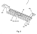
- Fig. 2 shows a three-dimensional view of a stack of load connection elements of the power semiconductor module according to the invention.
- Fig. 1 shows a section through an inventive power semiconductor module (1).
- This has a housing (3) with a frame-like housing part which is fixedly connected to the cooling member (2) of the arrangement.
- the frame-like housing part encloses the at least one substrate (5).
- This in turn has an insulating body (52), preferably an insulating ceramic, such as aluminum oxide or aluminum nitrite.
- the substrate (5) On the, the interior of the power semiconductor module (1) facing, the first main surface, the substrate (5) has a structured in itself Metallkaschtechnik.
- the individual sections of this metal lamination which is preferably configured as a copper lamination, form the printed conductors (54) of the power semiconductor module (1).
- the second main surface of the substrate (5) has a non-structured copper cladding (58) according to the prior art.
- controllable and / or uncontrolled power semiconductor devices such as IGBTs (insulated gate bipolar transistor) arranged in each case with antiparallel freewheeling diodes, or MOS-FETs. These are circuitally connected to other interconnects (54), for example by means of wire bonds (62) connected.
- the load connection elements (40, 42, 44) with the various necessary potentials serve for the external connection of the power electronic circuit in the interior of the power semiconductor module (1).
- the load connection elements (40, 42, 44) are formed as metal moldings, each having a band-like portion (402, 422, 442) parallel to the substrate surface.
- the band-like sections (402, 422, 442) form a stack (4, cf. Fig. 2 ), wherein the band-like portions of the individual load connection elements (40, 42, 44) in each case by means of an elastic intermediate layer (46) here a silicone pad spaced from each other and are electrically insulated from each other. It is particularly preferred if these silicone pads (46) are glued to the band-like sections, since thus the stack (4) is designed as a mounting unit. Necessary auxiliary connection elements are not shown for reasons of clarity in this sectional drawing.
- the power semiconductor module (1) preferably has an intermediate layer formed as an insulating molding (30) between the stack of strip-like sections (402, 422, 442) of the load connection elements (40, 42, 44) and the substrate (5).
- the insulating molding (30) has recesses (32) for passing through the contact feet (400, 420, 440) of the stack (4, cf. Fig. 2 ) on.
- the pressure device (70) for the thermal connection of the power semiconductor module (1) with a cooling component (2) and at the same time for electrically contacting the load connection elements (40, 42, 44) with the conductor tracks (54) of the substrate (5) is formed by a pressure element ( 72) for building up pressure on the stack (4, cf. Fig. 2
- the pressure element has pressure fingers (74) according to the prior art. It may also be preferred if between the pressure element (72) with flat lower side and the stack (4) a further elastic layer of the same configuration of the intermediate layer (46) is arranged.
- the pressure element (72) can furthermore be designed according to the prior art as a plastics molding with a suitable inner metal core and outer stiffening structures (76). It is also preferred if the pressure element (72) simultaneously serves as a cover of the power semiconductor module (1).
- Fig. 2 shows a three-dimensional view of a stack (4) of load connection elements (40, 42, 44) of the power semiconductor module according to the invention. Shown are the load connection elements (40, 42, 44), each having a plurality of contact feet (400, 420, 440) extending from the associated band-like portions (402, 422, 442).
- the contact devices (404, 424, 444) form the external terminals of the power semiconductor module.
- a resilient intermediate layer (46) each as a silicone pad with a minimum thickness of 1 mm.
- the respective elastic intermediate layer (46) simultaneously formed the electrical insulation of the adjacent load connection elements (40, 42, 44), as well as the pressure-transmitting and pressure-storing element of the power semiconductor module.
- load connection elements (40, 42, 44) in the region of the band-like sections (402, 422, 442) are connected to the respective intermediate layer (46) to form a mounting unit.
- This can be formed by way of example by a glued connection.
- a lamination method is used as the joining technique.
- the stack (4) further comprises recesses (406, 426, 446, 466) in the band-like sections (402, 422, 442) and the intermediate layer (46) for carrying out auxiliary connecting elements, not shown, formed as helical springs.
Landscapes
- Engineering & Computer Science (AREA)
- Microelectronics & Electronic Packaging (AREA)
- Power Engineering (AREA)
- Computer Hardware Design (AREA)
- Physics & Mathematics (AREA)
- Condensed Matter Physics & Semiconductors (AREA)
- General Physics & Mathematics (AREA)
- Manufacturing & Machinery (AREA)
- Mechanical Engineering (AREA)
- Cooling Or The Like Of Semiconductors Or Solid State Devices (AREA)
- Bipolar Transistors (AREA)
- Die Bonding (AREA)
Abstract
Description
Die Erfindung beschreibt ein Leistungshalbleitermodul in Druckkontaktausführung zur Anordnung auf einem Kühlbauteil. Einen Ausgangspunkt der Erfindung bilden Leistungshalbleitermodule wie sie beispielhaft aus der
Derartige Leistungshalbleitermodule bestehen nach dem Stand der Technik aus einem Gehäuse mit mindestens einem darin angeordneten elektrisch isolierenden Substrat vorzugsweise zur direkten Montage auf einem Kühlbauteil. Das Substrat seinerseits besteht aus einem Isolierstoffkörper mit einer Mehrzahl darauf befindlicher gegeneinander isolierter metallischer Verbindungsbahnen und hierauf befindlichen und mit diesen Verbindungsbahnen schaltungsgerecht verbundenen Leistungshalbleiterbauelementen. Weiterhin weisen die bekannten Leistungshalbleitermodule Anschlusselemente für externe Last- und Hilfsanschlüsse sowie im Inneren angeordnete Verbindungselemente auf. Diese Verbindungselemente für schaltungsgerechte Verbindungen im Inneren des Leistungshalbleitermoduls sind meist als Drahtbondverbindungen ausgebildet.Such power semiconductor modules according to the prior art consist of a housing with at least one electrically insulating substrate arranged therein, preferably for direct mounting on a cooling component. The substrate in turn consists of an insulating body with a plurality of mutually insulated metallic interconnect tracks located thereon and power semiconductor components located thereon and connected in a circuitally correct manner to these interconnect tracks. Furthermore, the known power semiconductor modules have connection elements for external load and auxiliary connections as well as connecting elements arranged in the interior. These connecting elements for circuit-compatible connections in the interior of the power semiconductor module are usually designed as Drahtbondverbindungen.
Ebenfalls bekannt sind Druck kontaktierte Leistungshalbleitermodule, wie sie aus der
Mittels einer derartigen Druckeinrichtung wird das Substrat auf ein Kühlbauteil gedrückt und somit der Wärmeübergang zwischen dem Substrat und dem Kühlbauteil dauerhaft sicher hergestellt. Das elastische Kissenelement dient hierbei der Aufrechterhaltung konstanter Druckverhältnisse bei unterschiedlichen thermischen Belastungen und über den gesamten Lebenszyklus des Leistungshalbleitermoduls.By means of such a pressure device, the substrate is pressed onto a cooling component and thus the heat transfer between the substrate and the cooling component is made permanently secure. The elastic cushion element serves to maintain constant pressure conditions at different thermal loads and over the entire life cycle of the power semiconductor module.
Die
Es sind auch weitergebildete Druckelemente bekannt, die an ihrer dem Substrat zugewandten Oberfläche eine Vielzahl von Druckfingern aufweisen. Vorzugsweise weist hierbei die Metallseele noch eine voreingestellte Durchbiegung auf. In der Kombination beider Maßnahmen kann ein derartiges Druckelement die gesamte Funktionalität einer oben genannten Druckeinrichtung bereitstellen.There are also known printing elements are known, which have on their surface facing the substrate a plurality of pressure fingers. Preferably, the metal core still has a preset deflection. In the combination of both measures, such a pressure element can provide the entire functionality of a printing device mentioned above.
Aus der
Weitere Leistungshalbleitermodule sind bekannt aus der
Der Erfindung liegt die Aufgabe zugrunde ein Leistungshalbleitermodul in Druckkontaktausführung vorzustellen, wobei die innere Isolation des Leistungshalbleitermoduls verbessert wird sowie die Ausbildung der Druckkontaktausführung vereinfacht wird.The invention has for its object to present a power semiconductor module in Druckkontaktausführung, wherein the internal insulation of the power semiconductor module is improved and the formation of the pressure contact design is simplified.
Die Aufgabe wird erfindungsgemäß gelöst, durch die Maßnahmen der Merkmale des Anspruchs 1. Bevorzugte Ausführungsformen sind in den Unteransprüchen beschrieben.The object is achieved by the measures of the features of
Der erfinderische Gedanke geht aus von einer Anordnung eines Leistungshalbleitermoduls in Druckkontaktausführung auf einem Kühlbauteil mit mindestens einem Substrat, mindestens zwei hierauf angeordneten Leistungshalbleiterbauelementen, beispielhaft bipolaren Transistoren, einem Gehäuse und nach außen führenden Last- und Steueranschlusselementen. Das Substrat selbst weist einen Isolierstoffkörper auf und auf dessen erster, dem Inneren des Leistungshalbleitermoduls zugewandten Hauptfläche Leiterbahnen mit Lastpotential. Weiterhin weist das Substrat vorzugsweise auch mindestens eine Leiterbahn mit Steuerpotential zu Ansteuerung der Leistungshalbleiterbauelemente auf.The inventive idea is based on an arrangement of a power semiconductor module in pressure contact design on a cooling component having at least one substrate, at least two power semiconductor components arranged thereon, for example bipolar transistors, a housing, and load and control connection elements leading to the outside. The substrate itself has an insulating body and on the first, the interior of the power semiconductor module facing the main surface traces with load potential. Furthermore, the substrate preferably also has at least one conductor track with control potential for driving the power semiconductor components.
Das Leistungshalbleitermodul weist weiterhin Lastanschlusselemente jeweils ausgebildet als Metallformkörper mit einer Kontakteinrichtung, einem bandartigen Abschnitt und mit einer Mehrzahl von diesem ausgehenden Kontaktfüßen auf. Die jeweiligen bandartige Abschnitte sind parallel zur Substratoberfläche und von dieser beabstandet angeordnet. Die Kontaktfüße, die von dem bandartigen Abschnitt ausgehen reichen zum Substrat und bilden dort schaltungsgerecht die Kontakte der Lastanschlüsse aus. Vorzugsweise kontaktieren sie hierzu auf dem Substrat die Leiterbahnen mit Lastpotential, alternativ auch direkt die Leistungshalbleiterbauelemente.The power semiconductor module further has load connection elements each formed as a metal molded body with a contact device, a band-like portion and with a plurality of this outgoing contact feet. The respective ribbon-like portions are arranged parallel to the substrate surface and spaced therefrom. The contact feet extending from the band-like portion extend to the substrate and there form the circuit of the contacts of the load terminals. For this purpose, they preferably contact the printed conductors with load potential on the substrate, alternatively alternatively directly the power semiconductor components.
Erfindungsgemäß bilden die Lastanschlusselemente einen Stapel wobei hierbei zwischen jeweils benachbarten Lastanschlusselementen im Bereich der jeweiligen bandartigen Abschnitte eine elastische Zwischenlage angeordnet ist. Diese Anordnung mehrerer elastischer Zwischenlage weist gegenüber dem Stand der Technik mit nur einem Druckspeicher, den Vorteil auf, dass die einzelnen Lastanschlusselement nicht starr sondern flexibel zueinander angeordnet sind und dadurch die Kontaktsicherheit wesentlich verbessert wird. Zudem werden Fertigungtoleranzen in der Länge der jeweiligen Kontaktfüße der einenzelene Lastanschlusselemente zueinander ausgeglichen. Durch die erfindungsgemäß Ausbildung des Stapels der Lastanschlusselemente drücken alle Kontaktfüße mit gleicher Kraft auf ihre jeweiligen Kontaktstellen auf dem Substrat bzw. auf den Leistungshalbleiterbauelementen.According to the invention, the load connection elements form a stack, wherein in this case an elastic intermediate layer is arranged between respectively adjacent load connection elements in the region of the respective strip-like sections. This arrangement of a plurality of elastic intermediate layer has over the prior art with only one pressure accumulator, the advantage that the individual load connection element are not rigidly but flexibly arranged to each other and thereby the contact reliability is significantly improved. In addition, manufacturing tolerances in the length of the respective contact feet of the individual load connection elements are compensated for one another. As a result of the design of the stack of load connection elements according to the invention, all contact feet press with the same force on their respective contact points on the substrate or on the power semiconductor components.
Besonders bevorzugt kann es sein, wenn die bandartigen Abschnitte der Lastanschlusselemente und die Kontaktfüße aus einem flächigen Metallkörper in Stanz-Biege- Technik hergestellt sind, mit dem Kontakteinrichtungen (404, 424, 444) verbunden werden und anschließend im mit elastischen Zwischenlage (46) zu einem Stapel (4) laminiert werden.It may be particularly preferred if the band-like portions of the load connection elements and the contact feet are made of a sheet metal body in punch-bending technique, are connected to the contact means (404, 424, 444) and then in with elastic intermediate layer (46) a stack (4) are laminated.
Dieses Herstellungsverfahren hat den Vorteil, dass durch den vorgefertigten Stapel, beim Zusammenbau des Leistungshalbleitermoduls nur wenige einzelnen Komponenten zueinander anzuordnen sind.This manufacturing method has the advantage that only a few individual components are to be arranged to each other by the prefabricated stack, when assembling the power semiconductor module.
Die erfinderische Lösung wird an Hand der Ausführungsbeispiele der
Auf der, dem Inneren des Leistungshalbleitermoduls (1) zugewandten, ersten Hauptfläche weist das Substrat (5) eine in sich strukturierte Metallkaschierung auf. Die einzelnen Abschnitte dieser vorzugsweise als Kupferkaschierung ausgestalteten Metallkaschierung bilden hierbei die Leiterbahnen (54) des Leistungshalbleitermoduls (1) aus. Die zweite Hauptfläche des Substrats (5) weist gemäß dem Stand der Technik eine nicht strukturierte Kupferkaschierung (58) auf.On the, the interior of the power semiconductor module (1) facing, the first main surface, the substrate (5) has a structured in itself Metallkaschierung. The individual sections of this metal lamination, which is preferably configured as a copper lamination, form the printed conductors (54) of the power semiconductor module (1). The second main surface of the substrate (5) has a non-structured copper cladding (58) according to the prior art.
Auf den Leiterbahnen (54) des Substrats (5) sind steuerbare und / oder ungesteuerte Leistungshalbleiterbauelemente (60) wie beispielhaft IGBTs (insulated gate bipolar Transistor) mit jeweils antiparallel geschalteten Freilaufdioden, oder MOS-FETs angeordnet. Diese sind schaltungsgerecht mit weiteren Leiterbahnen (54), beispielhaft mittels Drahtbondverbindungen (62), verbunden.On the interconnects (54) of the substrate (5) are controllable and / or uncontrolled power semiconductor devices (60) such as IGBTs (insulated gate bipolar transistor) arranged in each case with antiparallel freewheeling diodes, or MOS-FETs. These are circuitally connected to other interconnects (54), for example by means of wire bonds (62) connected.
Die Lastanschlusselemente (40, 42, 44) mit den verschiedenen notwendigen Potentialen dienen der externen Verbindung der leistungselektronischen Schaltung im Inneren des Leistungshalbleitermoduls (1). Hierzu sind die Lastanschlusselemente (40, 42, 44) als Metallformkörper ausgebildet, die je einen bandartigen Abschnitt (402, 422, 442) parallel zur Substratoberfläche aufweisen. Die bandartigen Abschnitte (402, 422, 442) bilden hierbei einen Stapel (4, vgl.
Vorzugsweise weist das erfindungsgemäße Leistungshalbleitermodul (1) eine als Isolierstoffformkörper (30) ausgebildete Zwischenlage zwischen dem Stapel der bandartigen Abschnitte (402, 422, 442) der Lastanschlusselemente (40, 42, 44) und dem Substrat (5) auf. Der lsolierstoffformkörper (30) weist Ausnehmungen (32) zur Durchführung der Kontaktfüße (400, 420, 440) des Stapels (4, vgl.
Die Druckeinrichtung (70) zur thermischen Verbindung des Leistungshalbleitermoduls (1) mit einem Kühlbauteil (2) und gleichzeitig zur elektrischen Kontaktierung der Lastanschlusselemente (40, 42, 44) mit den Leiterbahnen (54) des Substrats (5) wird gebildet durch ein Druckelement (72) zum Druckaufbau auf den Stapel (4, vgl.
Das Druckelement (72) kann weiterhin gemäß dem Stand der Technik als Kunststoffformkörper mit geeigneter innen liegender Metallseele und äußeren Versteifungsstrukturen (76) ausgeführt sein. Es ist ebenso bevorzugt, wenn das Druckelement (72) gleichzeitig als Deckel des Leistungshalbleitermoduls (1) dient.The pressure element (72) can furthermore be designed according to the prior art as a plastics molding with a suitable inner metal core and outer stiffening structures (76). It is also preferred if the pressure element (72) simultaneously serves as a cover of the power semiconductor module (1).
Zwischen den bandartigen Abschnitten (402, 422, 442) sind als elastische Zwischenlage (46) jeweils als ein Silikonkissen mit einer Mindestdicke von 1 mm angeordnet. Hierbei bildete die jeweilige elastische Zwischenlage (46) gleichzeitig die elektrische Isolation der benachbarten Lastanschlusselemente (40, 42, 44), sowie das Druck übertragende und Druck speichernde Element des Leistungshalbleitermoduls aus.Between the band-like portions (402, 422, 442) are arranged as a resilient intermediate layer (46) each as a silicone pad with a minimum thickness of 1 mm. In this case, the respective elastic intermediate layer (46) simultaneously formed the electrical insulation of the adjacent load connection elements (40, 42, 44), as well as the pressure-transmitting and pressure-storing element of the power semiconductor module.
Es ist besonders vorteilhaft, wenn die Lastanschlusselemente (40, 42, 44) im Bereich der bandartigen Abschnitte (402, 422, 442) mit den jeweiligen Zwischenlage (46) zu einer Montageeinheit verbunden sind. Dies kann beispielhaft durch eine Verklebeverbindung ausgebildet sein. Es ist allerdings besonders bevorzugt, wenn als Verbindungstechnik ein Laminierverfahren verwendet wird.It is particularly advantageous if the load connection elements (40, 42, 44) in the region of the band-like sections (402, 422, 442) are connected to the respective intermediate layer (46) to form a mounting unit. This can be formed by way of example by a glued connection. However, it is particularly preferred if a lamination method is used as the joining technique.
Der Stapel (4) weist weiterhin Ausnehmungen (406, 426, 446, 466) in den bandartigen Abschnitten (402, 422, 442) sowie den Zwischenlage (46) zur Durchführung von als Schraubenfedern ausgebildeten nicht dargestellten Hilfsanschlusselementen auf.The stack (4) further comprises recesses (406, 426, 446, 466) in the band-like sections (402, 422, 442) and the intermediate layer (46) for carrying out auxiliary connecting elements, not shown, formed as helical springs.
Claims (7)
- A power semiconductor module (1) in pressure contact design, for arranging on a heat sink (2), comprising at least one substrate (5), at least two power semiconductor components (60) disposed thereon, a housing (3) and outwardly-leading load (40, 42, 44) and control connection elements and comprising a pressure device (70) for introducing pressure onto the load connection elements for the electrical contacting thereof with conductor paths (54) of the substrate, wherein the substrate (5) comprises an insulating material body (52) and said conductor paths (54) with load potential are disposed on the first principal surface thereof, facing the interior of the power semiconductor module, wherein the load connection elements are each configured as metal shaped bodies having at least one contact element (404, 424), a strip-shaped section (402, 422, 442) and contact feet (400, 420, 440) emanating therefrom, the strip-shaped section is disposed parallel to the substrate surface and at a distance therefrom, and the contact feet extend from the strip-shaped section to the substrate (5) and contact these in a manner appropriate to the circuit, and wherein the load connection elements (40, 42, 44) form a stack and in this case, an elastic intermediate layer (46) is disposed between respectively adjacent load connection elements in the area of the respective strip-shaped sections (402, 422, 442).
- The power semiconductor module (1) according to claim 1, wherein the elastic intermediate layer (46) is configured as a silicone cushion having a minimum thickness of 1 mm.
- The power semiconductor module (1) according to claim 1, wherein the elastic intermediate layer (46) at the same time forms the electrical insulation of the load connection elements (40, 42, 44) adjacent hereto.
- The power semiconductor module (1) according to claim 3, wherein the load connection elements (40, 42, 44) are connected to form a unit in the area of the strip-shaped sections (402, 422, 442), all load connection elements are hereby electrically insulated with respect to one another and wherein the pressure device introduces pressure onto this stack and the contact feet (400, 420, 440) are thus connected to the conductor paths (54) of the substrate (5) in an electrically conducting manner.
- The power semiconductor module (1) according to claim 1, wherein a further elastic layer is disposed between a pressure element (72) of the pressure device (70) and the stack.
- The power semiconductor module (1) according to claim 1, wherein the stack (4) is configured by adhesive bonding.
- The power semiconductor module (1) according to any one of the aforesaid claims, wherein the pressure device (70) and the stack have recesses (406, 426, 446, 466) for the passage of auxiliary connecting elements configured as helical springs.
Applications Claiming Priority (1)
| Application Number | Priority Date | Filing Date | Title |
|---|---|---|---|
| DE102006006423A DE102006006423B4 (en) | 2006-02-13 | 2006-02-13 | Power semiconductor module and associated manufacturing method |
Publications (3)
| Publication Number | Publication Date |
|---|---|
| EP1830404A2 EP1830404A2 (en) | 2007-09-05 |
| EP1830404A3 EP1830404A3 (en) | 2008-05-07 |
| EP1830404B1 true EP1830404B1 (en) | 2009-08-05 |
Family
ID=38226586
Family Applications (1)
| Application Number | Title | Priority Date | Filing Date |
|---|---|---|---|
| EP07002031A Active EP1830404B1 (en) | 2006-02-13 | 2007-01-31 | Power semiconductor module |
Country Status (9)
| Country | Link |
|---|---|
| US (1) | US7683472B2 (en) |
| EP (1) | EP1830404B1 (en) |
| JP (1) | JP5186113B2 (en) |
| KR (1) | KR101238542B1 (en) |
| CN (1) | CN101026146B (en) |
| AT (1) | ATE438924T1 (en) |
| DE (2) | DE102006006423B4 (en) |
| DK (1) | DK1830404T3 (en) |
| ES (1) | ES2327964T3 (en) |
Families Citing this family (21)
| Publication number | Priority date | Publication date | Assignee | Title |
|---|---|---|---|---|
| DE102006006424B4 (en) * | 2006-02-13 | 2011-11-17 | Semikron Elektronik Gmbh & Co. Kg | Arrangement with at least one power semiconductor module and a cooling component and associated manufacturing method |
| DE102006006425B4 (en) * | 2006-02-13 | 2009-06-10 | Semikron Elektronik Gmbh & Co. Kg | Power semiconductor module in pressure contact design |
| DE102006052620B4 (en) * | 2006-11-08 | 2009-07-09 | Semikron Elektronik Gmbh & Co. Kg | Circuit arrangement with a power module that is combined with a printed circuit board. |
| DE102007003587B4 (en) | 2007-01-24 | 2009-06-10 | Semikron Elektronik Gmbh & Co. Kg | Power semiconductor module with pressure body |
| DE102007044046B4 (en) * | 2007-09-14 | 2013-01-03 | Infineon Technologies Ag | Method for internal contacting of a power semiconductor module |
| DE102008014112A1 (en) | 2008-03-13 | 2009-10-01 | Semikron Elektronik Gmbh & Co. Kg | Power semiconductor module for use on cooling component, has contact elements with contact section exhibiting deformation turned away from other contact section and forming contact surface for contacting with paths |
| DE102008014113B4 (en) | 2008-03-13 | 2014-04-03 | Semikron Elektronik Gmbh & Co. Kg | Power semiconductor module in pressure contact design |
| CN101582414B (en) * | 2009-04-02 | 2012-05-30 | 嘉兴斯达微电子有限公司 | Power module by directly bonding power terminal |
| DE102009057145B4 (en) | 2009-12-05 | 2013-12-19 | Semikron Elektronik Gmbh & Co. Kg | Pressure-contacted power semiconductor module with partially band-like load connection elements |
| DE102009057146B4 (en) * | 2009-12-05 | 2013-09-26 | Semikron Elektronik Gmbh & Co. Kg | Pressure-contacted power semiconductor module with hybrid pressure accumulator |
| DE102011008261A1 (en) * | 2011-01-11 | 2012-07-12 | Fraunhofer-Gesellschaft zur Förderung der angewandten Forschung e.V. | Rail for the electrical contacting of an electrically conductive substrate |
| CN106133903B (en) * | 2014-10-14 | 2019-01-01 | 富士电机株式会社 | Semiconductor device |
| US9431311B1 (en) | 2015-02-19 | 2016-08-30 | Semiconductor Components Industries, Llc | Semiconductor package with elastic coupler and related methods |
| DE102016115572B4 (en) | 2016-08-23 | 2019-06-13 | Semikron Elektronik Gmbh & Co. Kg | Power semiconductor device system having a first and a second power semiconductor device |
| WO2019053256A1 (en) | 2017-09-15 | 2019-03-21 | Finar Module Sagl | Packaging method and joint technology for an electronic device |
| DE102018112552B4 (en) * | 2018-05-25 | 2021-04-15 | Semikron Elektronik Gmbh & Co. Kg | Assembly with a plastic molded body and a plurality of load connection elements of a power semiconductor device and power semiconductor device with it |
| DE102018131855A1 (en) * | 2018-12-12 | 2020-06-18 | Semikron Elektronik Gmbh & Co. Kg | Power semiconductor module with a pressure body and with a pressure introduction body, power semiconductor arrangement hereby and power semiconductor system herewith |
| EP3736855A1 (en) | 2019-05-06 | 2020-11-11 | Infineon Technologies AG | Power semiconductor module arrangement and method for producing the same |
| EP3736858A1 (en) | 2019-05-06 | 2020-11-11 | Infineon Technologies AG | Power semiconductor module arrangement |
| EP3736854A1 (en) | 2019-05-06 | 2020-11-11 | Infineon Technologies AG | Power semiconductor module arrangement |
| DE102021205632A1 (en) | 2021-06-02 | 2022-12-08 | Zf Friedrichshafen Ag | Half bridge for an electric drive of an electric vehicle or a hybrid vehicle, power module for an inverter and inverter |
Family Cites Families (20)
| Publication number | Priority date | Publication date | Assignee | Title |
|---|---|---|---|---|
| DE3232168A1 (en) * | 1982-08-30 | 1984-03-01 | Siemens AG, 1000 Berlin und 8000 München | SEMICONDUCTOR COMPONENT WITH PRINT CONTACT |
| EP0138048B1 (en) * | 1983-09-29 | 1993-12-15 | Kabushiki Kaisha Toshiba | Press-packed semiconductor device |
| DE4237632A1 (en) * | 1992-11-07 | 1994-05-11 | Export Contor Ausenhandelsgese | Circuit arrangement |
| JP3396566B2 (en) * | 1995-10-25 | 2003-04-14 | 三菱電機株式会社 | Semiconductor device |
| DE19719703C5 (en) * | 1997-05-09 | 2005-11-17 | eupec Europäische Gesellschaft für Leistungshalbleiter mbH & Co. KG | Power semiconductor module with ceramic substrate |
| DE19843309A1 (en) * | 1998-09-22 | 2000-03-23 | Asea Brown Boveri | Short-circuit proof IGBT module |
| DE19903875C2 (en) * | 1999-02-01 | 2001-11-29 | Semikron Elektronik Gmbh | Power semiconductor circuit arrangement, in particular current converter, in pressure contact |
| JP2002076259A (en) * | 2000-08-28 | 2002-03-15 | Mitsubishi Electric Corp | Power module |
| DE10121970B4 (en) * | 2001-05-05 | 2004-05-27 | Semikron Elektronik Gmbh | Power semiconductor module in pressure contact |
| DE10127947C1 (en) * | 2001-08-22 | 2002-10-17 | Semikron Elektronik Gmbh | Circuit device for power semiconductor module has intermediate circuit board with DC and AC terminals coupled to conductor paths of substrate incorporated in base body |
| DE10141114C1 (en) * | 2001-06-08 | 2002-11-21 | Semikron Elektronik Gmbh | Circuit device has AC terminal element of circuit substrate cooled via terminal pin of base body thermally connected to heat sink |
| EP1318545A1 (en) * | 2001-12-06 | 2003-06-11 | Abb Research Ltd. | Power semiconductor submodule and power semiconductor module |
| EP1367643B1 (en) * | 2002-05-15 | 2006-04-05 | Tyco Electronics AMP GmbH | Electronic module |
| JP3669971B2 (en) * | 2002-05-21 | 2005-07-13 | 三菱電機株式会社 | Semiconductor module |
| US6946740B2 (en) * | 2002-07-15 | 2005-09-20 | International Rectifier Corporation | High power MCM package |
| DE102004025609B4 (en) * | 2004-05-25 | 2010-12-09 | Semikron Elektronik Gmbh & Co. Kg | Arrangement in screw-type pressure contact with a power semiconductor module |
| DE102004061936A1 (en) * | 2004-12-22 | 2006-07-06 | Siemens Ag | Arrangement of a semiconductor module and an electrical busbar |
| US7443014B2 (en) * | 2005-10-25 | 2008-10-28 | Infineon Technologies Ag | Electronic module and method of assembling the same |
| DE102006006424B4 (en) * | 2006-02-13 | 2011-11-17 | Semikron Elektronik Gmbh & Co. Kg | Arrangement with at least one power semiconductor module and a cooling component and associated manufacturing method |
| DE102006006425B4 (en) * | 2006-02-13 | 2009-06-10 | Semikron Elektronik Gmbh & Co. Kg | Power semiconductor module in pressure contact design |
-
2006
- 2006-02-13 DE DE102006006423A patent/DE102006006423B4/en not_active Expired - Fee Related
-
2007
- 2007-01-22 KR KR1020070006579A patent/KR101238542B1/en active IP Right Grant
- 2007-01-31 EP EP07002031A patent/EP1830404B1/en active Active
- 2007-01-31 DE DE502007001210T patent/DE502007001210D1/en active Active
- 2007-01-31 ES ES07002031T patent/ES2327964T3/en active Active
- 2007-01-31 AT AT07002031T patent/ATE438924T1/en active
- 2007-01-31 DK DK07002031T patent/DK1830404T3/en active
- 2007-02-09 JP JP2007030495A patent/JP5186113B2/en not_active Expired - Fee Related
- 2007-02-12 CN CN2007100052665A patent/CN101026146B/en not_active Expired - Fee Related
- 2007-02-13 US US11/705,719 patent/US7683472B2/en not_active Expired - Fee Related
Also Published As
| Publication number | Publication date |
|---|---|
| DE102006006423B4 (en) | 2009-06-10 |
| DE102006006423A1 (en) | 2007-08-23 |
| KR101238542B1 (en) | 2013-02-28 |
| US20070187817A1 (en) | 2007-08-16 |
| DK1830404T3 (en) | 2009-11-02 |
| JP5186113B2 (en) | 2013-04-17 |
| CN101026146B (en) | 2010-09-29 |
| CN101026146A (en) | 2007-08-29 |
| US7683472B2 (en) | 2010-03-23 |
| ES2327964T3 (en) | 2009-11-05 |
| DE502007001210D1 (en) | 2009-09-17 |
| JP2007221127A (en) | 2007-08-30 |
| ATE438924T1 (en) | 2009-08-15 |
| KR20070081743A (en) | 2007-08-17 |
| EP1830404A2 (en) | 2007-09-05 |
| EP1830404A3 (en) | 2008-05-07 |
Similar Documents
| Publication | Publication Date | Title |
|---|---|---|
| EP1830404B1 (en) | Power semiconductor module | |
| EP1843393B1 (en) | Pressure contact type power semiconductor module | |
| DE102006006424B4 (en) | Arrangement with at least one power semiconductor module and a cooling component and associated manufacturing method | |
| DE102006027481C5 (en) | Power semiconductor module with mutually electrically insulated connection elements | |
| DE102009037257B4 (en) | Power semiconductor module with circuit carrier and load connection element and manufacturing method thereof | |
| DE102017109706B3 (en) | Power electronic arrangement with DC voltage connection element | |
| EP1933379B1 (en) | Power semiconductor module with contact springs | |
| DE102007006212B4 (en) | Power semiconductor module with contact springs | |
| EP1855319A2 (en) | Power semiconductor device | |
| EP2091080B1 (en) | Power semiconductor module with a substrate and a pressure device | |
| EP1840961A2 (en) | High performance semiconductor module and associated manufacturing method | |
| DE102005055713B4 (en) | Power semiconductor module with connection elements | |
| EP1933380A2 (en) | Power semiconductor module with contact springs | |
| EP1950807B1 (en) | Power semiconductor module with pressure body | |
| EP2341535B1 (en) | Pressure-contacted power semiconductor module with hybrid pressure accumulator | |
| EP2003693B1 (en) | Pressure contact three-phase converter module | |
| DE102008014113B4 (en) | Power semiconductor module in pressure contact design | |
| EP2330623A1 (en) | Pressure-contacted high performance semiconductor module with some tape-like load connection elements | |
| DE102018111594A1 (en) | Power semiconductor module and power semiconductor device with a power semiconductor module |
Legal Events
| Date | Code | Title | Description |
|---|---|---|---|
| PUAI | Public reference made under article 153(3) epc to a published international application that has entered the european phase |
Free format text: ORIGINAL CODE: 0009012 |
|
| AK | Designated contracting states |
Kind code of ref document: A2 Designated state(s): AT BE BG CH CY CZ DE DK EE ES FI FR GB GR HU IE IS IT LI LT LU LV MC NL PL PT RO SE SI SK TR |
|
| AX | Request for extension of the european patent |
Extension state: AL BA HR MK YU |
|
| PUAL | Search report despatched |
Free format text: ORIGINAL CODE: 0009013 |
|
| AK | Designated contracting states |
Kind code of ref document: A3 Designated state(s): AT BE BG CH CY CZ DE DK EE ES FI FR GB GR HU IE IS IT LI LT LU LV MC NL PL PT RO SE SI SK TR |
|
| AX | Request for extension of the european patent |
Extension state: AL BA HR MK RS |
|
| 17P | Request for examination filed |
Effective date: 20080423 |
|
| 17Q | First examination report despatched |
Effective date: 20080623 |
|
| RTI1 | Title (correction) |
Free format text: POWER SEMICONDUCTOR MODULE |
|
| GRAP | Despatch of communication of intention to grant a patent |
Free format text: ORIGINAL CODE: EPIDOSNIGR1 |
|
| AKX | Designation fees paid |
Designated state(s): AT BE BG CH CY CZ DE DK EE ES FI FR GB GR HU IE IS IT LI LT LU LV MC NL PL PT RO SE SI SK TR |
|
| GRAS | Grant fee paid |
Free format text: ORIGINAL CODE: EPIDOSNIGR3 |
|
| GRAA | (expected) grant |
Free format text: ORIGINAL CODE: 0009210 |
|
| AK | Designated contracting states |
Kind code of ref document: B1 Designated state(s): AT BE BG CH CY CZ DE DK EE ES FI FR GB GR HU IE IS IT LI LT LU LV MC NL PL PT RO SE SI SK TR |
|
| REG | Reference to a national code |
Ref country code: GB Ref legal event code: FG4D Free format text: NOT ENGLISH |
|
| REG | Reference to a national code |
Ref country code: CH Ref legal event code: NV Representative=s name: BRAUNPAT BRAUN EDER AG Ref country code: CH Ref legal event code: EP |
|
| REG | Reference to a national code |
Ref country code: IE Ref legal event code: FG4D |
|
| REF | Corresponds to: |
Ref document number: 502007001210 Country of ref document: DE Date of ref document: 20090917 Kind code of ref document: P |
|
| REG | Reference to a national code |
Ref country code: DK Ref legal event code: T3 |
|
| REG | Reference to a national code |
Ref country code: ES Ref legal event code: FG2A Ref document number: 2327964 Country of ref document: ES Kind code of ref document: T3 |
|
| REG | Reference to a national code |
Ref country code: SE Ref legal event code: TRGR |
|
| REG | Reference to a national code |
Ref country code: SK Ref legal event code: T3 Ref document number: E 6118 Country of ref document: SK |
|
| LTIE | Lt: invalidation of european patent or patent extension |
Effective date: 20090805 |
|
| PG25 | Lapsed in a contracting state [announced via postgrant information from national office to epo] |
Ref country code: IS Free format text: LAPSE BECAUSE OF FAILURE TO SUBMIT A TRANSLATION OF THE DESCRIPTION OR TO PAY THE FEE WITHIN THE PRESCRIBED TIME-LIMIT Effective date: 20091205 Ref country code: LT Free format text: LAPSE BECAUSE OF FAILURE TO SUBMIT A TRANSLATION OF THE DESCRIPTION OR TO PAY THE FEE WITHIN THE PRESCRIBED TIME-LIMIT Effective date: 20090805 |
|
| PG25 | Lapsed in a contracting state [announced via postgrant information from national office to epo] |
Ref country code: PL Free format text: LAPSE BECAUSE OF FAILURE TO SUBMIT A TRANSLATION OF THE DESCRIPTION OR TO PAY THE FEE WITHIN THE PRESCRIBED TIME-LIMIT Effective date: 20090805 Ref country code: LV Free format text: LAPSE BECAUSE OF FAILURE TO SUBMIT A TRANSLATION OF THE DESCRIPTION OR TO PAY THE FEE WITHIN THE PRESCRIBED TIME-LIMIT Effective date: 20090805 Ref country code: SI Free format text: LAPSE BECAUSE OF FAILURE TO SUBMIT A TRANSLATION OF THE DESCRIPTION OR TO PAY THE FEE WITHIN THE PRESCRIBED TIME-LIMIT Effective date: 20090805 |
|
| REG | Reference to a national code |
Ref country code: IE Ref legal event code: FD4D |
|
| PG25 | Lapsed in a contracting state [announced via postgrant information from national office to epo] |
Ref country code: PT Free format text: LAPSE BECAUSE OF FAILURE TO SUBMIT A TRANSLATION OF THE DESCRIPTION OR TO PAY THE FEE WITHIN THE PRESCRIBED TIME-LIMIT Effective date: 20091205 Ref country code: BG Free format text: LAPSE BECAUSE OF FAILURE TO SUBMIT A TRANSLATION OF THE DESCRIPTION OR TO PAY THE FEE WITHIN THE PRESCRIBED TIME-LIMIT Effective date: 20091105 |
|
| PG25 | Lapsed in a contracting state [announced via postgrant information from national office to epo] |
Ref country code: EE Free format text: LAPSE BECAUSE OF FAILURE TO SUBMIT A TRANSLATION OF THE DESCRIPTION OR TO PAY THE FEE WITHIN THE PRESCRIBED TIME-LIMIT Effective date: 20090805 Ref country code: RO Free format text: LAPSE BECAUSE OF FAILURE TO SUBMIT A TRANSLATION OF THE DESCRIPTION OR TO PAY THE FEE WITHIN THE PRESCRIBED TIME-LIMIT Effective date: 20090805 Ref country code: IE Free format text: LAPSE BECAUSE OF FAILURE TO SUBMIT A TRANSLATION OF THE DESCRIPTION OR TO PAY THE FEE WITHIN THE PRESCRIBED TIME-LIMIT Effective date: 20090805 Ref country code: CZ Free format text: LAPSE BECAUSE OF FAILURE TO SUBMIT A TRANSLATION OF THE DESCRIPTION OR TO PAY THE FEE WITHIN THE PRESCRIBED TIME-LIMIT Effective date: 20090805 |
|
| PLBE | No opposition filed within time limit |
Free format text: ORIGINAL CODE: 0009261 |
|
| STAA | Information on the status of an ep patent application or granted ep patent |
Free format text: STATUS: NO OPPOSITION FILED WITHIN TIME LIMIT |
|
| 26N | No opposition filed |
Effective date: 20100507 |
|
| BERE | Be: lapsed |
Owner name: SEMIKRON ELEKTRONIK G.M.B.H. & CO. KG Effective date: 20100131 |
|
| PG25 | Lapsed in a contracting state [announced via postgrant information from national office to epo] |
Ref country code: MC Free format text: LAPSE BECAUSE OF NON-PAYMENT OF DUE FEES Effective date: 20100131 |
|
| PG25 | Lapsed in a contracting state [announced via postgrant information from national office to epo] |
Ref country code: GR Free format text: LAPSE BECAUSE OF FAILURE TO SUBMIT A TRANSLATION OF THE DESCRIPTION OR TO PAY THE FEE WITHIN THE PRESCRIBED TIME-LIMIT Effective date: 20091106 |
|
| PG25 | Lapsed in a contracting state [announced via postgrant information from national office to epo] |
Ref country code: BE Free format text: LAPSE BECAUSE OF NON-PAYMENT OF DUE FEES Effective date: 20100131 |
|
| PGRI | Patent reinstated in contracting state [announced from national office to epo] |
Ref country code: IT Effective date: 20110501 |
|
| PG25 | Lapsed in a contracting state [announced via postgrant information from national office to epo] |
Ref country code: CY Free format text: LAPSE BECAUSE OF FAILURE TO SUBMIT A TRANSLATION OF THE DESCRIPTION OR TO PAY THE FEE WITHIN THE PRESCRIBED TIME-LIMIT Effective date: 20090805 |
|
| PG25 | Lapsed in a contracting state [announced via postgrant information from national office to epo] |
Ref country code: LU Free format text: LAPSE BECAUSE OF NON-PAYMENT OF DUE FEES Effective date: 20100131 Ref country code: HU Free format text: LAPSE BECAUSE OF FAILURE TO SUBMIT A TRANSLATION OF THE DESCRIPTION OR TO PAY THE FEE WITHIN THE PRESCRIBED TIME-LIMIT Effective date: 20100206 |
|
| PG25 | Lapsed in a contracting state [announced via postgrant information from national office to epo] |
Ref country code: TR Free format text: LAPSE BECAUSE OF FAILURE TO SUBMIT A TRANSLATION OF THE DESCRIPTION OR TO PAY THE FEE WITHIN THE PRESCRIBED TIME-LIMIT Effective date: 20090805 |
|
| REG | Reference to a national code |
Ref country code: FR Ref legal event code: PLFP Year of fee payment: 10 |
|
| REG | Reference to a national code |
Ref country code: FR Ref legal event code: PLFP Year of fee payment: 11 |
|
| PGFP | Annual fee paid to national office [announced via postgrant information from national office to epo] |
Ref country code: NL Payment date: 20170124 Year of fee payment: 11 |
|
| PGFP | Annual fee paid to national office [announced via postgrant information from national office to epo] |
Ref country code: SE Payment date: 20170125 Year of fee payment: 11 Ref country code: FI Payment date: 20170120 Year of fee payment: 11 |
|
| PGFP | Annual fee paid to national office [announced via postgrant information from national office to epo] |
Ref country code: AT Payment date: 20170120 Year of fee payment: 11 Ref country code: SK Payment date: 20170124 Year of fee payment: 11 Ref country code: DK Payment date: 20170125 Year of fee payment: 11 |
|
| REG | Reference to a national code |
Ref country code: FR Ref legal event code: PLFP Year of fee payment: 12 |
|
| REG | Reference to a national code |
Ref country code: CH Ref legal event code: PCAR Free format text: NEW ADDRESS: HOLEESTRASSE 87, 4054 BASEL (CH) |
|
| REG | Reference to a national code |
Ref country code: DK Ref legal event code: EBP Effective date: 20180131 |
|
| REG | Reference to a national code |
Ref country code: NL Ref legal event code: MM Effective date: 20180201 |
|
| REG | Reference to a national code |
Ref country code: AT Ref legal event code: MM01 Ref document number: 438924 Country of ref document: AT Kind code of ref document: T Effective date: 20180131 |
|
| REG | Reference to a national code |
Ref country code: SK Ref legal event code: MM4A Ref document number: E 6118 Country of ref document: SK Effective date: 20180131 |
|
| REG | Reference to a national code |
Ref country code: SE Ref legal event code: EUG |
|
| PG25 | Lapsed in a contracting state [announced via postgrant information from national office to epo] |
Ref country code: FI Free format text: LAPSE BECAUSE OF NON-PAYMENT OF DUE FEES Effective date: 20180131 Ref country code: SE Free format text: LAPSE BECAUSE OF NON-PAYMENT OF DUE FEES Effective date: 20180201 |
|
| PG25 | Lapsed in a contracting state [announced via postgrant information from national office to epo] |
Ref country code: AT Free format text: LAPSE BECAUSE OF NON-PAYMENT OF DUE FEES Effective date: 20180131 Ref country code: SK Free format text: LAPSE BECAUSE OF NON-PAYMENT OF DUE FEES Effective date: 20180131 Ref country code: NL Free format text: LAPSE BECAUSE OF NON-PAYMENT OF DUE FEES Effective date: 20180201 |
|
| PG25 | Lapsed in a contracting state [announced via postgrant information from national office to epo] |
Ref country code: DK Free format text: LAPSE BECAUSE OF NON-PAYMENT OF DUE FEES Effective date: 20180131 |
|
| PGFP | Annual fee paid to national office [announced via postgrant information from national office to epo] |
Ref country code: CH Payment date: 20210122 Year of fee payment: 15 Ref country code: FR Payment date: 20210120 Year of fee payment: 15 Ref country code: IT Payment date: 20210129 Year of fee payment: 15 |
|
| PGFP | Annual fee paid to national office [announced via postgrant information from national office to epo] |
Ref country code: DE Payment date: 20210131 Year of fee payment: 15 Ref country code: ES Payment date: 20210217 Year of fee payment: 15 Ref country code: GB Payment date: 20210122 Year of fee payment: 15 |
|
| REG | Reference to a national code |
Ref country code: DE Ref legal event code: R119 Ref document number: 502007001210 Country of ref document: DE |
|
| REG | Reference to a national code |
Ref country code: CH Ref legal event code: PL |
|
| GBPC | Gb: european patent ceased through non-payment of renewal fee |
Effective date: 20220131 |
|
| PG25 | Lapsed in a contracting state [announced via postgrant information from national office to epo] |
Ref country code: GB Free format text: LAPSE BECAUSE OF NON-PAYMENT OF DUE FEES Effective date: 20220131 Ref country code: DE Free format text: LAPSE BECAUSE OF NON-PAYMENT OF DUE FEES Effective date: 20220802 |
|
| PG25 | Lapsed in a contracting state [announced via postgrant information from national office to epo] |
Ref country code: FR Free format text: LAPSE BECAUSE OF NON-PAYMENT OF DUE FEES Effective date: 20220131 |
|
| PG25 | Lapsed in a contracting state [announced via postgrant information from national office to epo] |
Ref country code: LI Free format text: LAPSE BECAUSE OF NON-PAYMENT OF DUE FEES Effective date: 20220131 Ref country code: CH Free format text: LAPSE BECAUSE OF NON-PAYMENT OF DUE FEES Effective date: 20220131 |
|
| REG | Reference to a national code |
Ref country code: ES Ref legal event code: FD2A Effective date: 20230303 |
|
| PG25 | Lapsed in a contracting state [announced via postgrant information from national office to epo] |
Ref country code: ES Free format text: LAPSE BECAUSE OF NON-PAYMENT OF DUE FEES Effective date: 20220201 |