EP1826830A2 - Photovoltaic apparatus and method of manufacturing the same - Google Patents
Photovoltaic apparatus and method of manufacturing the same Download PDFInfo
- Publication number
- EP1826830A2 EP1826830A2 EP07250625A EP07250625A EP1826830A2 EP 1826830 A2 EP1826830 A2 EP 1826830A2 EP 07250625 A EP07250625 A EP 07250625A EP 07250625 A EP07250625 A EP 07250625A EP 1826830 A2 EP1826830 A2 EP 1826830A2
- Authority
- EP
- European Patent Office
- Prior art keywords
- groove
- photoelectric conversion
- electrode
- back electrode
- forming
- Prior art date
- Legal status (The legal status is an assumption and is not a legal conclusion. Google has not performed a legal analysis and makes no representation as to the accuracy of the status listed.)
- Withdrawn
Links
- 238000004519 manufacturing process Methods 0.000 title claims description 31
- 239000000758 substrate Substances 0.000 claims abstract description 100
- 238000006243 chemical reaction Methods 0.000 claims description 122
- 230000008018 melting Effects 0.000 claims description 5
- 238000002844 melting Methods 0.000 claims description 5
- 229910021417 amorphous silicon Inorganic materials 0.000 description 12
- 230000000052 comparative effect Effects 0.000 description 12
- 229910021424 microcrystalline silicon Inorganic materials 0.000 description 11
- 239000004065 semiconductor Substances 0.000 description 9
- 229910052710 silicon Inorganic materials 0.000 description 8
- 239000010703 silicon Substances 0.000 description 8
- XUIMIQQOPSSXEZ-UHFFFAOYSA-N Silicon Chemical compound [Si] XUIMIQQOPSSXEZ-UHFFFAOYSA-N 0.000 description 7
- BQCADISMDOOEFD-UHFFFAOYSA-N Silver Chemical compound [Ag] BQCADISMDOOEFD-UHFFFAOYSA-N 0.000 description 6
- 238000000034 method Methods 0.000 description 6
- 230000008569 process Effects 0.000 description 6
- 229910052709 silver Inorganic materials 0.000 description 6
- 239000004332 silver Substances 0.000 description 6
- 239000000463 material Substances 0.000 description 5
- 239000000155 melt Substances 0.000 description 4
- 230000010355 oscillation Effects 0.000 description 4
- TWNQGVIAIRXVLR-UHFFFAOYSA-N oxo(oxoalumanyloxy)alumane Chemical compound O=[Al]O[Al]=O TWNQGVIAIRXVLR-UHFFFAOYSA-N 0.000 description 4
- 238000007650 screen-printing Methods 0.000 description 4
- XLOMVQKBTHCTTD-UHFFFAOYSA-N Zinc monoxide Chemical compound [Zn]=O XLOMVQKBTHCTTD-UHFFFAOYSA-N 0.000 description 3
- 239000003822 epoxy resin Substances 0.000 description 3
- 239000002245 particle Substances 0.000 description 3
- 229920000647 polyepoxide Polymers 0.000 description 3
- XOLBLPGZBRYERU-UHFFFAOYSA-N tin dioxide Chemical compound O=[Sn]=O XOLBLPGZBRYERU-UHFFFAOYSA-N 0.000 description 3
- 238000011109 contamination Methods 0.000 description 2
- 230000000694 effects Effects 0.000 description 2
- 238000002474 experimental method Methods 0.000 description 2
- 239000007769 metal material Substances 0.000 description 2
- 230000004048 modification Effects 0.000 description 2
- 238000012986 modification Methods 0.000 description 2
- 238000005268 plasma chemical vapour deposition Methods 0.000 description 2
- HBMJWWWQQXIZIP-UHFFFAOYSA-N silicon carbide Chemical compound [Si+]#[C-] HBMJWWWQQXIZIP-UHFFFAOYSA-N 0.000 description 2
- 238000004544 sputter deposition Methods 0.000 description 2
- 229910001887 tin oxide Inorganic materials 0.000 description 2
- 230000015572 biosynthetic process Effects 0.000 description 1
- 238000005229 chemical vapour deposition Methods 0.000 description 1
- 239000011521 glass Substances 0.000 description 1
- 230000002401 inhibitory effect Effects 0.000 description 1
- 238000005259 measurement Methods 0.000 description 1
- 239000000203 mixture Substances 0.000 description 1
- 230000009467 reduction Effects 0.000 description 1
- 230000004044 response Effects 0.000 description 1
- 150000003376 silicon Chemical class 0.000 description 1
- 229910010271 silicon carbide Inorganic materials 0.000 description 1
- 238000009751 slip forming Methods 0.000 description 1
- 238000002230 thermal chemical vapour deposition Methods 0.000 description 1
- 239000011787 zinc oxide Substances 0.000 description 1
Images


Classifications
-
- H—ELECTRICITY
- H10—SEMICONDUCTOR DEVICES; ELECTRIC SOLID-STATE DEVICES NOT OTHERWISE PROVIDED FOR
- H10F—INORGANIC SEMICONDUCTOR DEVICES SENSITIVE TO INFRARED RADIATION, LIGHT, ELECTROMAGNETIC RADIATION OF SHORTER WAVELENGTH OR CORPUSCULAR RADIATION
- H10F71/00—Manufacture or treatment of devices covered by this subclass
- H10F71/10—Manufacture or treatment of devices covered by this subclass the devices comprising amorphous semiconductor material
- H10F71/103—Manufacture or treatment of devices covered by this subclass the devices comprising amorphous semiconductor material including only Group IV materials
-
- H—ELECTRICITY
- H10—SEMICONDUCTOR DEVICES; ELECTRIC SOLID-STATE DEVICES NOT OTHERWISE PROVIDED FOR
- H10F—INORGANIC SEMICONDUCTOR DEVICES SENSITIVE TO INFRARED RADIATION, LIGHT, ELECTROMAGNETIC RADIATION OF SHORTER WAVELENGTH OR CORPUSCULAR RADIATION
- H10F10/00—Individual photovoltaic cells, e.g. solar cells
- H10F10/10—Individual photovoltaic cells, e.g. solar cells having potential barriers
- H10F10/17—Photovoltaic cells having only PIN junction potential barriers
- H10F10/172—Photovoltaic cells having only PIN junction potential barriers comprising multiple PIN junctions, e.g. tandem cells
-
- H—ELECTRICITY
- H10—SEMICONDUCTOR DEVICES; ELECTRIC SOLID-STATE DEVICES NOT OTHERWISE PROVIDED FOR
- H10F—INORGANIC SEMICONDUCTOR DEVICES SENSITIVE TO INFRARED RADIATION, LIGHT, ELECTROMAGNETIC RADIATION OF SHORTER WAVELENGTH OR CORPUSCULAR RADIATION
- H10F19/00—Integrated devices, or assemblies of multiple devices, comprising at least one photovoltaic cell covered by group H10F10/00, e.g. photovoltaic modules
- H10F19/30—Integrated devices, or assemblies of multiple devices, comprising at least one photovoltaic cell covered by group H10F10/00, e.g. photovoltaic modules comprising thin-film photovoltaic cells
- H10F19/31—Integrated devices, or assemblies of multiple devices, comprising at least one photovoltaic cell covered by group H10F10/00, e.g. photovoltaic modules comprising thin-film photovoltaic cells having multiple laterally adjacent thin-film photovoltaic cells deposited on the same substrate
-
- H—ELECTRICITY
- H10—SEMICONDUCTOR DEVICES; ELECTRIC SOLID-STATE DEVICES NOT OTHERWISE PROVIDED FOR
- H10F—INORGANIC SEMICONDUCTOR DEVICES SENSITIVE TO INFRARED RADIATION, LIGHT, ELECTROMAGNETIC RADIATION OF SHORTER WAVELENGTH OR CORPUSCULAR RADIATION
- H10F19/00—Integrated devices, or assemblies of multiple devices, comprising at least one photovoltaic cell covered by group H10F10/00, e.g. photovoltaic modules
- H10F19/30—Integrated devices, or assemblies of multiple devices, comprising at least one photovoltaic cell covered by group H10F10/00, e.g. photovoltaic modules comprising thin-film photovoltaic cells
- H10F19/31—Integrated devices, or assemblies of multiple devices, comprising at least one photovoltaic cell covered by group H10F10/00, e.g. photovoltaic modules comprising thin-film photovoltaic cells having multiple laterally adjacent thin-film photovoltaic cells deposited on the same substrate
- H10F19/33—Patterning processes to connect the photovoltaic cells, e.g. laser cutting of conductive or active layers
-
- H—ELECTRICITY
- H10—SEMICONDUCTOR DEVICES; ELECTRIC SOLID-STATE DEVICES NOT OTHERWISE PROVIDED FOR
- H10F—INORGANIC SEMICONDUCTOR DEVICES SENSITIVE TO INFRARED RADIATION, LIGHT, ELECTROMAGNETIC RADIATION OF SHORTER WAVELENGTH OR CORPUSCULAR RADIATION
- H10F19/00—Integrated devices, or assemblies of multiple devices, comprising at least one photovoltaic cell covered by group H10F10/00, e.g. photovoltaic modules
- H10F19/30—Integrated devices, or assemblies of multiple devices, comprising at least one photovoltaic cell covered by group H10F10/00, e.g. photovoltaic modules comprising thin-film photovoltaic cells
- H10F19/31—Integrated devices, or assemblies of multiple devices, comprising at least one photovoltaic cell covered by group H10F10/00, e.g. photovoltaic modules comprising thin-film photovoltaic cells having multiple laterally adjacent thin-film photovoltaic cells deposited on the same substrate
- H10F19/35—Structures for the connecting of adjacent photovoltaic cells, e.g. interconnections or insulating spacers
-
- H—ELECTRICITY
- H10—SEMICONDUCTOR DEVICES; ELECTRIC SOLID-STATE DEVICES NOT OTHERWISE PROVIDED FOR
- H10F—INORGANIC SEMICONDUCTOR DEVICES SENSITIVE TO INFRARED RADIATION, LIGHT, ELECTROMAGNETIC RADIATION OF SHORTER WAVELENGTH OR CORPUSCULAR RADIATION
- H10F71/00—Manufacture or treatment of devices covered by this subclass
- H10F71/10—Manufacture or treatment of devices covered by this subclass the devices comprising amorphous semiconductor material
- H10F71/103—Manufacture or treatment of devices covered by this subclass the devices comprising amorphous semiconductor material including only Group IV materials
- H10F71/1035—Manufacture or treatment of devices covered by this subclass the devices comprising amorphous semiconductor material including only Group IV materials having multiple Group IV elements, e.g. SiGe or SiC
-
- Y—GENERAL TAGGING OF NEW TECHNOLOGICAL DEVELOPMENTS; GENERAL TAGGING OF CROSS-SECTIONAL TECHNOLOGIES SPANNING OVER SEVERAL SECTIONS OF THE IPC; TECHNICAL SUBJECTS COVERED BY FORMER USPC CROSS-REFERENCE ART COLLECTIONS [XRACs] AND DIGESTS
- Y02—TECHNOLOGIES OR APPLICATIONS FOR MITIGATION OR ADAPTATION AGAINST CLIMATE CHANGE
- Y02E—REDUCTION OF GREENHOUSE GAS [GHG] EMISSIONS, RELATED TO ENERGY GENERATION, TRANSMISSION OR DISTRIBUTION
- Y02E10/00—Energy generation through renewable energy sources
- Y02E10/50—Photovoltaic [PV] energy
- Y02E10/547—Monocrystalline silicon PV cells
-
- Y—GENERAL TAGGING OF NEW TECHNOLOGICAL DEVELOPMENTS; GENERAL TAGGING OF CROSS-SECTIONAL TECHNOLOGIES SPANNING OVER SEVERAL SECTIONS OF THE IPC; TECHNICAL SUBJECTS COVERED BY FORMER USPC CROSS-REFERENCE ART COLLECTIONS [XRACs] AND DIGESTS
- Y02—TECHNOLOGIES OR APPLICATIONS FOR MITIGATION OR ADAPTATION AGAINST CLIMATE CHANGE
- Y02E—REDUCTION OF GREENHOUSE GAS [GHG] EMISSIONS, RELATED TO ENERGY GENERATION, TRANSMISSION OR DISTRIBUTION
- Y02E10/00—Energy generation through renewable energy sources
- Y02E10/50—Photovoltaic [PV] energy
- Y02E10/548—Amorphous silicon PV cells
-
- Y—GENERAL TAGGING OF NEW TECHNOLOGICAL DEVELOPMENTS; GENERAL TAGGING OF CROSS-SECTIONAL TECHNOLOGIES SPANNING OVER SEVERAL SECTIONS OF THE IPC; TECHNICAL SUBJECTS COVERED BY FORMER USPC CROSS-REFERENCE ART COLLECTIONS [XRACs] AND DIGESTS
- Y02—TECHNOLOGIES OR APPLICATIONS FOR MITIGATION OR ADAPTATION AGAINST CLIMATE CHANGE
- Y02P—CLIMATE CHANGE MITIGATION TECHNOLOGIES IN THE PRODUCTION OR PROCESSING OF GOODS
- Y02P70/00—Climate change mitigation technologies in the production process for final industrial or consumer products
- Y02P70/50—Manufacturing or production processes characterised by the final manufactured product
Definitions
- the present invention relates to a photovoltaic apparatus and a method of manufacturing the same, and more particularly, it relates to a photovoltaic apparatus comprising a conductive intermediate layer between a plurality of photoelectric conversion portions and a method of manufacturing the same.
- a photovoltaic apparatus comprising a conductive intermediate layer between a plurality of photoelectric conversion units (photoelectric conversion portions) is known in general, as disclosed in Japanese Patent Laying-Open No. 2002-118273 , for example.
- first and second transparent electrodes are formed on a substrate at a prescribed interval, while a first photoelectric conversion unit is formed on the first and second transparent electrodes.
- a second photoelectric conversion unit is formed on the first photoelectric conversion unit through a conductive intermediate layer.
- First and second back electrodes are arranged on the second photoelectric conversion unit to correspond to the aforementioned first and second transparent electrodes respectively.
- the first back electrode is electrically connected to the second transparent electrode through a groove so formed as to pass through the second photoelectric conversion unit, the intermediate layer and the first photoelectric conversion unit.
- the first back electrode is in contact with the conductive intermediate in the groove, to disadvantageously result in an electrical short circuit between the first back electrode and the intermediate layer.
- the present invention has been proposed in the light of the aforementioned problem, and a preferred aim is to provide a photovoltaic apparatus, comprising a conductive intermediate layer between a plurality of photoelectric conversion portions, capable of suppressing an electrical short circuit between a back electrode and the intermediate layer and a method of manufacturing the same.
- a photovoltaic apparatus comprises a substrate having an insulating surface, a first substrate electrode and a second substrate electrode formed on the insulating surface of the substrate and isolated from each other by a first groove, a first photoelectric conversion portion so formed as to cover the first substrate electrode and the second substrate electrode, a second photoelectric conversion portion formed on the surface of the first photoelectric conversion portion through a conductive intermediate layer, a first back electrode and a second back electrode, formed on the surface of the second photoelectric conversion portion, corresponding to the first substrate electrode and the second substrate electrode respectively, a second groove for electrically isolating the first back electrode and the second back electrode from each other, a third groove formed on a region located between the first groove and the second groove to cut at least the intermediate layer from the upper surface of the second back electrode, a first insulating member embedded in the third groove to cover at least a cut portion of the intermediate layer and a conductive member electrically connected to the first substrate electrode on
- the photovoltaic apparatus is provided with the third groove so formed as to cut at least the intermediate layer from the upper surface of the second back electrode on the region located between the first groove for electrically isolating the first and second substrate electrodes from each other and the second groove for electrically isolating the first and second back electrodes from each other respectively and the first insulating member embedded in the third groove to cover at least the cut portion of the intermediate layer, whereby the first insulating member can electrically insulate portions of the intermediate layer closer to the first and second grooves with respect to the third groove respectively from each other.
- the photovoltaic apparatus is provided with the conductive member electrically connected to the first substrate electrode on the region located between the second groove for electrically isolating the first and second back electrodes from each other and the third groove filled up with the first insulating member and electrically connected to the second back electrode across the third groove, whereby the conductive member, electrically insulated from the portion of the intermediate layer closer to the first groove with respect to the third groove by the aforementioned first insulating member, can be inhibited from an electrical short circuit with the portion of the intermediate layer closer to the first groove with respect to the third groove.
- the conductive member is provided independently of the back electrodes so that a manufacturing process of subsequently forming the back electrodes after forming the second photoelectric conversion portion and thereafter forming the conductive member can be employed, whereby the surface of the second photoelectric conversion portion, to be most inhibited from contamination in the process of manufacturing the photovoltaic apparatus, can be prevented from exposure to the atmosphere.
- the aforementioned photovoltaic apparatus preferably further comprises a fourth groove formed on the region located between the second groove and the third groove to pass through the second back electrode, the second photoelectric conversion portion, the intermediate layer and the first photoelectric conversion portion and expose the surface of the first substrate electrode, and the conductive member is preferably embedded in the fourth groove to come into contact with the surface of the first substrate electrode exposed in the fourth groove and formed to be electrically connected to the second back electrode across the first insulating member embedded in the third groove.
- the conductive member embedded in the fourth groove electrically insulated from the portion of the intermediate layer closer to the first groove with respect to the third groove by the first insulating member embedded in the third groove, can be inhibited from an electrical short circuit with the portion of the intermediate layer closer to the first groove with respect to the third groove.
- the conductive member preferably includes a conductive melt portion obtained by partially melting the second back electrode, the second photoelectric conversion portion, the intermediate layer and the first photoelectric conversion portion and electrically connected to the first substrate electrode and a connecting portion formed to be electrically connected to the melt portion and to be electrically connected to the second back electrode across the first insulating member embedded in the third groove on the region located between the second groove and the third groove.
- the quantity of the material constituting the connecting portion can be reduced due to the melt portion as compared with a case of connecting the first substrate electrode and the second back electrode with each other only through the material constituting the connecting portion.
- the first insulating member preferably fills up the third groove.
- the conductive member can be reliably electrically insulated from the portion of the intermediate layer closer to the first groove with respect to the third groove.
- the upper surface of the first insulating member may be so formed as to project upward beyond the upper surface of the second back electrode.
- the conductive member may be so formed as to come into contact with the surface of a region of the second back electrode located between the first groove and the third groove.
- the second groove may be so formed as to pass through the second back electrode, the second photoelectric conversion portion, the intermediate layer and the first photoelectric conversion portion and expose the surface of the first substrate electrode.
- the third groove is preferably so formed as to pass through the second back electrode, the second photoelectric conversion portion, the intermediate layer and the first photoelectric conversion portion and expose the surface of the first substrate electrode.
- the second back electrode, the second photoelectric conversion portion, the intermediate layer and the first photoelectric conversion portion can be parted through the third groove, whereby portions of the second back electrode, the second photoelectric conversion portion, the intermediate layer and the first photoelectric conversion portion closer to the first groove with respect to the third groove and those of the second back electrode, the second photoelectric conversion portion, the intermediate layer and the first photoelectric conversion portion closer to the conductive member with respect to the third groove can be inhibited from electrical connection.
- adjacent photovoltaic elements can be easily electrically insulated from each other through the third groove.
- the aforementioned photovoltaic apparatus preferably further comprises a second insulating member embedded in the second groove.
- the conductive member so formed as to connect the first substrate electrode and the second back electrode with each other can be inhibited from entering the second groove.
- the photovoltaic apparatus can be inhibited from an electrical short circuit resulting from the conductive member entering the second groove.
- the second insulating member preferably fills up the second groove. According to this structure, the conductive member can be reliably prevented from entering the second groove.
- the intermediate layer may have a function of partly reflecting and partly transmitting light incident from the side of the substrate.
- a method of manufacturing a photovoltaic apparatus comprises steps of forming a substrate electrode on an insulating surface of a substrate having the insulating surface, forming a first substrate electrode and a second substrate electrode isolated from each other by a first groove by forming the first groove on the substrate electrode, forming a first photoelectric conversion portion to cover the first substrate electrode and the second substrate electrode, forming a second photoelectric conversion portion on the surface of the first photoelectric conversion portion through a conductive intermediate layer, forming a back electrode on the surface of the second photoelectric conversion portion, thereafter forming a second groove for separating the back electrode into a first back electrode and a second back electrode while forming a third groove on a region located between the first groove and the second groove to pass through at least the intermediate layer from the upper surface of the second back electrode, forming a first insulating member in the third groove to cover at least a cut portion of the intermediate layer and forming a conductive member electrically connected to the first substrate electrode on a region located between
- the aforementioned method of manufacturing a photovoltaic apparatus preferably further comprises a step of forming a fourth groove on the region located between the second groove and the third groove to pass through the second back electrode, the second photovoltaic conversion portion, the intermediate layer and the first photoelectric conversion portion and expose the surface of the first substrate electrode, and the step of forming the conductive member preferably includes a step of embedding the conductive member in the fourth groove to come into contact with the surface of the first substrate electrode exposed in the fourth groove while electrically connecting the conductive member to the second back electrode across the first insulating member embedded in the third groove.
- the conductive member embedded in the fourth groove electrically insulated from a portion of the intermediate layer closer to the first groove with respect to the third groove through the first insulating member embedded in the third groove, can be so provided as to cause no electrical short circuit with the portion of the intermediate layer closer to the first groove with respect to the third groove.
- the step of forming the second groove and the third groove is preferably carried out substantially simultaneously with the step of forming the fourth groove. According to this structure, the steps of manufacturing the photovoltaic apparatus can be simplified.
- the step of forming the conductive member may include a step of forming the conductive member to come into contact with a region of the second back electrode located between the first groove and the third groove.
- the step of forming the conductive member preferably includes steps of forming a conductive melt portion electrically connected to the first substrate electrode by partially melting the second back electrode, the second photoelectric conversion portion, the intermediate layer and the first photoelectric conversion portion on the region located between the second groove and the third groove and forming a connecting portion to be electrically connected to the melt portion and to be electrically connected to the second back electrode across the first insulating member embedded in the third groove.
- the first substrate electrode and the second back electrode can be electrically connected to each other by forming the connecting portion with a smaller quantity of material due to the melt portion as compared with a case of connecting the first substrate electrode and the second back electrode with each other only through the material constituting the connecting portion.
- the step of forming the third groove preferably includes a step of forming the third groove to pass through the second back electrode, the second photoelectric conversion portion, the intermediate layer and the first photoelectric conversion portion and expose the surface of the first substrate electrode.
- the second back electrode, the second photoelectric conversion portion, the intermediate layer and the first photoelectric conversion portion can be parted through the third groove, whereby portions of the second back electrode, the second photoelectric conversion portion, the intermediate layer and the first photoelectric conversion portion closer to the first groove with respect to the third groove and those of the second back electrode, the second photoelectric conversion portion, the intermediate layer and the first photoelectric conversion portion closer to the conductive member with respect to the third groove can be inhibited from electrical connection.
- the conductive member and the portion of the intermediate layer closer to the first groove with respect to the third groove can be inhibited from electrical connection.
- the step of forming the first insulating member preferably includes a step of filling the third groove with the first insulating member. According to this structure, the conductive member and the portion of the intermediate layer closer to the first groove with respect to the third groove can be reliably electrically insulated from each other.
- the step of forming the second groove may include a step of forming the second groove to pass through the second back electrode, the second photoelectric conversion portion, the intermediate layer and the first photoelectric conversion portion and expose the surface of the first substrate electrode.
- the method of manufacturing a photovoltaic apparatus preferably further comprises a step of filling the second groove with a second insulating member.
- the conductive member so formed as to connect the first substrate electrode and the second back electrode with each other can be inhibited from entering the second groove.
- the photovoltaic apparatus can be inhibited from an electrical short circuit resulting from the conductive member entering the second groove.
- the photovoltaic apparatus 1 As shown in Fig. 1, the photovoltaic apparatus 1 according to the first embodiment comprises a substrate 2, substrate electrodes 3a and 3b, a photoelectric conversion unit 4, an intermediate layer 5, another photoelectric conversion unit 6, back electrodes 7a and 7b, an insulating member 8 and a connecting electrode 9.
- This photovoltaic apparatus 1 according to the first embodiment is formed by serially connecting a plurality of units with each other in a direction along the main surface of the substrate 2 through the connecting electrode 9. The structure of the photovoltaic apparatus 1 is now described in detail.
- the substrate 2 having an insulating surface, consists of translucent glass. This substrate 2 has a thickness of about 1 mm to about 5 mm.
- the substrate electrodes 3a and 3b isolated from each other by a groove 3c are formed on the upper surface of the substrate 2.
- TCO transparent conductive oxide
- the substrate electrodes 3a and 3b are examples of the "first substrate electrode” and the "second substrate electrode” in the present invention respectively, and the groove 3c is an example of the "first groove” in the present invention.
- the photoelectric conversion unit 4 consisting of a p-i-n amorphous silicon semiconductor is formed on the upper surfaces of the substrate electrodes 3a and 3b.
- This photoelectric conversion unit 4 of the p-i-n amorphous silicon semiconductor is constituted of a p-type hydrogenated amorphous silicon carbide (a-SiC:H) layer having a thickness of about 10 nm to about 20 nm, an i-type hydrogenated amorphous silicon (a-Si:H) layer having a thickness of about 250 nm to about 350 nm and an n-type hydrogenated amorphous silicon layer having a thickness of about 20 nm to about 30 nm.
- a-SiC:H p-type hydrogenated amorphous silicon carbide
- a-Si:H i-type hydrogenated amorphous silicon
- n-type hydrogenated amorphous silicon layer having a thickness of about 20 nm to about 30 nm.
- the photoelectric conversion unit 4 is formed on the upper surface of the substrate electrode 3a to have grooves 4a, 4b and 4c and fill up the groove 3c.
- the photoelectric conversion unit 4 of the amorphous silicon semiconductor is formed for absorbing light of a relatively short wavelength.
- This photoelectric conversion unit 4 is an example of the "first photoelectric conversion portion" in the present invention.
- the intermediate layer 5 having grooves 5a, 5b and 5c on regions corresponding to the regions 4a, 4b and 4c respectively is formed on the upper surface of the photoelectric conversion unit 4.
- This intermediate layer 5 has a thickness of about 10 nm to about 500 nm.
- the intermediate layer 5 consists of TCO such as zinc oxide (ZnO) having conductivity with a function of partly reflecting and partly transmitting light incident from the side of the substrate 2.
- the intermediate layer 5 also has a function of increasing the quantity of light passing through the photoelectric conversion unit 4 by partly reflecting the light incident from the side of the substrate 2. Therefore, an output current of the photoelectric conversion unit 4 can be increased without increasing the thickness thereof.
- the output current of the photoelectric conversion unit 4 can be increased while suppressing photo-deterioration remarkably increased in response to the thickness of the photoelectric conversion unit 4 of the amorphous silicon semiconductor.
- the output currents of the photoelectric conversion units 4 and 6 can be balanced.
- the photoelectric conversion unit 6 of a p-i-n microcrystalline silicon semiconductor having grooves 6a, 6b and 6c on regions corresponding to the grooves 5a, 5b and 5c respectively is formed on the upper surface of the intermediate layer 5.
- This photoelectric conversion unit 6 of the p-i-n microcrystalline silicon semiconductor is constituted of a p-type hydrogenated microcrystalline silicon ( ⁇ c-Si:H) layer having a thickness of about 10 nm to about 20 nm, an i-type hydrogenated microcrystalline silicon layer having a thickness of about 1500 nm to about 2000 nm and an n-type hydrogenated microcrystalline silicon layer having a thickness of about 20 nm to about 30 nm.
- the photoelectric conversion unit 6 of the p-i-n microcrystalline silicon semiconductor is formed for absorbing light of a relatively long wavelength.
- the photoelectric conversion unit 6 is an example of the "second photoelectric conversion portion" in the present invention.
- the back electrodes 7a and 7b isolated from each other by a groove 7d formed on a region corresponding to the groove 6b are formed on the upper surface of the photoelectric conversion unit 6.
- the back electrode 7b has grooves 7c and 7e on regions corresponding to the grooves 6a and 6c respectively.
- the back electrodes 7a and 7b are examples of the "first back electrode” and the "second back electrode” in the present invention respectively.
- the grooves 4b, 5b, 6b and 7d constitute a groove 20a for electrically isolating the back electrodes 7a and 7b from each other, while the grooves 4c, 5c, 6c and 7e constitute a groove 20b for electrically isolating portions of the intermediate layer 5 from each other. Further, the grooves 4a, 5a, 6a and 7c constitute a groove 20c for electrically connecting the back electrode 7b and the substrate electrode 3a with each other.
- the grooves 20a, 20b and 20c are so formed as to pass through a back electrode 7 (back electrodes 7a and 7b), the photoelectric conversion unit 6, the intermediate layer 5 and the photoelectric conversion unit 4 and expose the surface of the substrate electrode 3a.
- the grooves 20a, 20b and 20c are examples of the "second groove", the "third groove” and the "fourth groove” in the present invention respectively.
- the insulating member 8 consists of epoxy resin containing aluminum oxide (Al 2 O 3 ) particles, and is so embedded as to fill up the groove 20b.
- the insulating member 8 is so embedded as to electrically insulate portions of the groove 5c of the intermediate layer 5 located closer to the grooves 3c and 5a respectively from each other.
- the upper surface of the insulating member 8 is so provided as to protrude upward beyond the upper surface of the back electrode 7b.
- the insulating member 8 is an example of the "first insulating member" in the present invention.
- the connecting electrode 9 consists of conductive paste (silver paste).
- This connecting electrode 9 is embedded in the groove 20c to come into contact with the surface of the substrate electrode 3a exposed in the groove 20c, and formed to be electrically connected to the upper surface of a region of the back electrode 7b of the adjacent unit located between the grooves 3c and 20b across the insulating member 8.
- the substrate electrode 3a and the back electrode 7b of the adjacent unit are serially connected with each other.
- the connecting electrode 9 is an example of the "conductive member" in the present invention.
- a substrate electrode 3 of tin oxide having a thickness of about 800 nm is formed on the insulating upper surface of the substrate 2 by thermal CVD (chemical vapor deposition).
- the groove 3c is formed by scanning the substrate electrode 3 with a fundamental wave LB1 of an Nd:YAG laser having a wavelength of about 1064 nm, an oscillation frequency of about 20 kHz and average power of about 14.0 W from above.
- the substrate electrode 3 is separated into the substrate electrodes 3a and 3b through the groove 3c.
- the photoelectric conversion unit 4 of the amorphous silicon semiconductor is formed by successively forming the p-type hydrogenated amorphous silicon carbide layer having the thickness of about 10 nm to about 20 nm, the i-type hydrogenated amorphous silicon layer having the thickness of about 250 nm to about 350 nm and the n-type hydrogenated amorphous silicon layer having the thickness of about 20 nm to about 30 nm on the upper surfaces of the substrate electrodes 3a and 3b by plasma CVD. Thereafter the intermediate layer 5 of zinc oxide having the thickness of about 10 nm to about 500 nm is formed on the upper surface of the photoelectric conversion unit 4 by sputtering.
- the photoelectric conversion unit 6 of the microcrystalline silicon semiconductor is formed by successively forming the p-type hydrogenated microcrystalline silicon layer having the thickness of about 10 nm to about 20 nm, the i-type hydrogenated microcrystalline silicon layer having the thickness of about 1500 nm to about 2000 nm and the n-type hydrogenated microcrystalline silicon layer having the thickness of about 20 nm to about 30 nm on the upper surface of the intermediate layer 5 by plasma CVD.
- the photoelectric conversion unit 4, the intermediate layer 5, the photoelectric conversion unit 6 and the back electrode 7 are so continuously formed that the surfaces of the photoelectric conversion unit 4, the intermediate layer 5 and the photoelectric conversion unit 6 are not exposed to the atmosphere.
- the groove 20a constituted of the grooves 4b, 5b, 6b and 7d, the groove 20b constituted of the grooves 4c, 5c, 6c and 7e and the groove 20c constituted of the grooves 4a, 5a, 6a and 7c are simultaneously formed to be adjacent to the groove 3c by scanning the photoelectric conversion unit 4, the intermediate layer 5, the photoelectric conversion unit 6 and the back electrode 7 with second harmonics LB2 of an Nd:YAG laser having a wavelength of about 532 nm, an oscillation frequency of about 12 kHz and average power of about 230 mW from the side of the substrate 2.
- the back electrode 7 is separated into the back electrodes 7a and 7b through the groove 20a.
- the insulating member 8 of epoxy resin containing aluminum oxide particles is applied by screen printing, to fill up the groove 20b and extend onto the back electrode 7b. Thereafter the connecting electrode 9 is applied by screen printing, to fill up the groove 20c and be electrically connected to the back electrode 7b across the insulating member 8, as shown in Fig. 1.
- the photovoltaic apparatus 1 is provided with the groove 20b so formed as to cut the intermediate layer 5 on the region located between the groove 3c for electrically isolating the substrate electrodes 3a and 3b from each other and the groove 20a for electrically isolating the back electrodes 7a and 7b from each other as well as the insulating member 8 embedded in the groove 20b, so that the insulating member 8 can electrically insulate the portions of the intermediate layer 5 closer to the grooves 3c and 20c with respect to the groove 20b respectively from each other.
- the connecting electrode 9 is provided independently of the back electrode 7 so that the manufacturing process of subsequently forming the back electrode 7 after forming the second photoelectric conversion unit 6 and thereafter forming the groove 20c while forming the connecting member 9 in this groove 20c can be employed, whereby the surface of the photoelectric conversion unit 6, to be most inhibited from contamination in the process of manufacturing the photovoltaic apparatus 1, can be prevented from exposure to the atmosphere.
- photovoltaic apparatuses 1 and 101 according to Example 1 and comparative example 1 were prepared as follows:
- the photovoltaic apparatus 1 according to Example 1 was prepared as shown in Fig. 1, through the manufacturing process employed in the first embodiment.
- the photovoltaic apparatus 101 according to comparative example 1 was prepared to have a structure shown in Fig. 7.
- a photoelectric conversion unit 104, an intermediate layer 105, another photoelectric conversion unit 106 and back electrodes 107a and 107b of the photovoltaic apparatus 101 according to comparative example 1 were so formed as to have the same thicknesses and compositions as those of a photoelectric conversion unit 4, an intermediate layer 5, another photoelectric conversion unit 6 and back electrodes 7a and 7b of the photovoltaic apparatus 1 according to Example 1 respectively.
- the photovoltaic apparatus 101 according to comparative example 1 was formed with only grooves 120a and 120c corresponding to grooves 20a and 20c among grooves 20a, 20b and 20c of the photovoltaic apparatus 1 according to Example 1 respectively.
- the back electrode 107b was directly embedded in the groove 120c, to be electrically connected to a substrate electrode 3a.
- the open circuit voltage of the photovoltaic apparatus 1 according to Example 1 is identical to that of the photovoltaic apparatus 101 according to comparative example 1. It has also been proved that the short circuit current and the fill factor of the photovoltaic apparatus 1 according to Example 1 are improved by 4 % and 1 % with respect to those of the photovoltaic apparatus 101 according to comparative example 1 respectively. It has further been proved that the maximum power and the conversion efficiency of the photovoltaic apparatus 1 according to Example 1 are improved by 5 % and 5 % with respect to those of the photovoltaic apparatus 101 according to comparative example 1 respectively.
- an insulating member 8 electrically isolates a connecting electrode 9 from a portion of the intermediate layer 5 closer to a groove 3c with respect to the groove 20b for inhibiting the connecting electrode 9 from an electrical short circuit with the portion of the intermediate layer 5 closer to the groove 3c with respect to the groove 20b, thereby conceivably improving the conversion efficiency.
- the back electrode 107b embedded in the groove 120c is in contact with the intermediate layer 5 in this groove 120c to cause an electrical short circuit with the intermediate layer 105, conceivably resulting in reduction of the conversion efficiency.
- a silicon melt 22 and a connecting electrode 23 electrically connect a substrate electrode 3a and a back electrode 7b with each other in a photovoltaic apparatus 21 according to a second embodiment of the present invention, dissimilarly to the aforementioned first embodiment.
- the silicon melt 22 is formed in a region located between grooves 20a and 20b by partially melting a photoelectric conversion unit 4, an intermediate layer 5, another photoelectric conversion unit 6 and the back electrode 7b in the photovoltaic apparatus 21 according to the second embodiment.
- This silicon melt 22 has conductivity, and is electrically connected to the substrate electrode 3a.
- the silicon melt 22 is an example of the "melt portion" or the "conductive member" in the present invention.
- the connecting electrode 23 is electrically connected with the silicon melt 22, and electrically connected to another back electrode 7b across an insulating member 8 embedded in the groove 20b.
- the connecting electrode 23 is an example of the "connecting portion" or the "conductive member” in the present invention.
- a process of manufacturing the photovoltaic apparatus 21 according to the second embodiment of the present invention is now described with reference to Figs. 8 to 11. Steps up to formation of a back electrode 7 are similar to those for the photovoltaic apparatus 1 according to the first embodiment shown in Figs. 2 to 4.
- the groove 20a constituted of grooves 4b, 5b, 6b and 7d and the groove 20b constituted of grooves 4c, 5c, 6c and 7e are simultaneously formed to be adjacent to the groove 3c by scanning the photoelectric conversion unit 4, the intermediate layer 5, the photoelectric conversion unit 6 and the back electrode 7 with second harmonics LB3 of an Nd:YAG laser having a wavelength of about 532 nm, an oscillation frequency of about 12 kHz and average power of about 230 mW from the side of a substrate 2, as shown in Fig. 9.
- the back electrode 7 is separated into the back electrodes 7a and 7b through the groove 20a.
- the photoelectric conversion unit 4, the intermediate layer 5, the photoelectric conversion unit 6 and the back electrode 7b are scanned with a fundamental wave LB4 of an Nd:YAG laser having a wavelength of about 1064 nm, an oscillation frequency of about 20 kHz and average power of about 8 W on the region located between the grooves 20a and 20b from the side of the back electrode 7b to be partially melted, thereby forming the silicon melt 22.
- the insulating member 8 of epoxy resin containing aluminum oxide particles is applied by screen printing to fill up the groove 20b and extend onto the back electrode 7b, as shown in Fig. 11.
- the connecting electrode 23 of silver paste is applied by screen printing, to come into contact with the surface of the silicon melt 22 and be electrically connected to the back electrode 7b across the insulating member 8.
- the silicon melt 22 and the connecting electrode 23 electrically connect the substrate electrode 3a and the back electrode 7b with each other, whereby the quantity of the material for the connecting electrode 23 of silver paste can be reduced as compared with the first embodiment connecting the substrate electrode 3a and the back electrode 7b with each other only through the connecting electrode 9.
- the present invention is not restricted to this but a groove 7d may separate back electrodes 7a and 7b from each other and an insulating member 10 may fill up a groove 20a constituted of grooves 4b, 5b, 6b and 7d, as in a photovoltaic apparatus according to a modification of the first embodiment shown in Fig. 12.
- the photovoltaic apparatus can be inhibited from an electrical short circuit resulting from silver paste entering the groove 20a when a connecting electrode 9 or 23 is screen-printed.
- the insulating member 10 is an example of the "second insulating member" in the present invention.
- the present invention is not restricted to this but at least the groove 5c may be formed to be filled up with the insulating member 8 for covering at least a cut portion of the groove 5c.
Landscapes
- Photovoltaic Devices (AREA)
Abstract
Description
- The present invention relates to a photovoltaic apparatus and a method of manufacturing the same, and more particularly, it relates to a photovoltaic apparatus comprising a conductive intermediate layer between a plurality of photoelectric conversion portions and a method of manufacturing the same.
- A photovoltaic apparatus comprising a conductive intermediate layer between a plurality of photoelectric conversion units (photoelectric conversion portions) is known in general, as disclosed in
Japanese Patent Laying-Open No. 2002-118273 - In the photovoltaic apparatus disclosed in the aforementioned
Japanese Patent Laying-Open No. 2002-118273 - In the photovoltaic apparatus disclosed in the aforementioned
Japanese Patent Laying-Open No. 2002-118273 - The present invention has been proposed in the light of the aforementioned problem, and a preferred aim is to provide a photovoltaic apparatus, comprising a conductive intermediate layer between a plurality of photoelectric conversion portions, capable of suppressing an electrical short circuit between a back electrode and the intermediate layer and a method of manufacturing the same.
- In order to attain the aforementioned object, a photovoltaic apparatus according to a first aspect of the present invention comprises a substrate having an insulating surface, a first substrate electrode and a second substrate electrode formed on the insulating surface of the substrate and isolated from each other by a first groove, a first photoelectric conversion portion so formed as to cover the first substrate electrode and the second substrate electrode, a second photoelectric conversion portion formed on the surface of the first photoelectric conversion portion through a conductive intermediate layer, a first back electrode and a second back electrode, formed on the surface of the second photoelectric conversion portion, corresponding to the first substrate electrode and the second substrate electrode respectively, a second groove for electrically isolating the first back electrode and the second back electrode from each other, a third groove formed on a region located between the first groove and the second groove to cut at least the intermediate layer from the upper surface of the second back electrode, a first insulating member embedded in the third groove to cover at least a cut portion of the intermediate layer and a conductive member electrically connected to the first substrate electrode on a region located between the second groove and the third groove and electrically connected to the second back electrode across the third groove.
- As hereinabove described, the photovoltaic apparatus according to the first aspect is provided with the third groove so formed as to cut at least the intermediate layer from the upper surface of the second back electrode on the region located between the first groove for electrically isolating the first and second substrate electrodes from each other and the second groove for electrically isolating the first and second back electrodes from each other respectively and the first insulating member embedded in the third groove to cover at least the cut portion of the intermediate layer, whereby the first insulating member can electrically insulate portions of the intermediate layer closer to the first and second grooves with respect to the third groove respectively from each other. Further, the photovoltaic apparatus is provided with the conductive member electrically connected to the first substrate electrode on the region located between the second groove for electrically isolating the first and second back electrodes from each other and the third groove filled up with the first insulating member and electrically connected to the second back electrode across the third groove, whereby the conductive member, electrically insulated from the portion of the intermediate layer closer to the first groove with respect to the third groove by the aforementioned first insulating member, can be inhibited from an electrical short circuit with the portion of the intermediate layer closer to the first groove with respect to the third groove. In addition, the conductive member is provided independently of the back electrodes so that a manufacturing process of subsequently forming the back electrodes after forming the second photoelectric conversion portion and thereafter forming the conductive member can be employed, whereby the surface of the second photoelectric conversion portion, to be most inhibited from contamination in the process of manufacturing the photovoltaic apparatus, can be prevented from exposure to the atmosphere.
- The aforementioned photovoltaic apparatus according to the first aspect preferably further comprises a fourth groove formed on the region located between the second groove and the third groove to pass through the second back electrode, the second photoelectric conversion portion, the intermediate layer and the first photoelectric conversion portion and expose the surface of the first substrate electrode, and the conductive member is preferably embedded in the fourth groove to come into contact with the surface of the first substrate electrode exposed in the fourth groove and formed to be electrically connected to the second back electrode across the first insulating member embedded in the third groove. According to this structure, the conductive member embedded in the fourth groove, electrically insulated from the portion of the intermediate layer closer to the first groove with respect to the third groove by the first insulating member embedded in the third groove, can be inhibited from an electrical short circuit with the portion of the intermediate layer closer to the first groove with respect to the third groove.
- In the aforementioned photovoltaic apparatus according to the first aspect, the conductive member preferably includes a conductive melt portion obtained by partially melting the second back electrode, the second photoelectric conversion portion, the intermediate layer and the first photoelectric conversion portion and electrically connected to the first substrate electrode and a connecting portion formed to be electrically connected to the melt portion and to be electrically connected to the second back electrode across the first insulating member embedded in the third groove on the region located between the second groove and the third groove. According to this structure, the quantity of the material constituting the connecting portion can be reduced due to the melt portion as compared with a case of connecting the first substrate electrode and the second back electrode with each other only through the material constituting the connecting portion.
- In the aforementioned photovoltaic apparatus according to the first aspect, the first insulating member preferably fills up the third groove. According to this structure, the conductive member can be reliably electrically insulated from the portion of the intermediate layer closer to the first groove with respect to the third groove.
- In this case, the upper surface of the first insulating member may be so formed as to project upward beyond the upper surface of the second back electrode.
- In the aforementioned photovoltaic apparatus according to the first aspect, the conductive member may be so formed as to come into contact with the surface of a region of the second back electrode located between the first groove and the third groove.
- In the aforementioned photovoltaic apparatus according to the first aspect, the second groove may be so formed as to pass through the second back electrode, the second photoelectric conversion portion, the intermediate layer and the first photoelectric conversion portion and expose the surface of the first substrate electrode.
- In the aforementioned photovoltaic apparatus according to the first aspect, the third groove is preferably so formed as to pass through the second back electrode, the second photoelectric conversion portion, the intermediate layer and the first photoelectric conversion portion and expose the surface of the first substrate electrode. According to this structure, the second back electrode, the second photoelectric conversion portion, the intermediate layer and the first photoelectric conversion portion can be parted through the third groove, whereby portions of the second back electrode, the second photoelectric conversion portion, the intermediate layer and the first photoelectric conversion portion closer to the first groove with respect to the third groove and those of the second back electrode, the second photoelectric conversion portion, the intermediate layer and the first photoelectric conversion portion closer to the conductive member with respect to the third groove can be inhibited from electrical connection. Thus, adjacent photovoltaic elements can be easily electrically insulated from each other through the third groove.
- The aforementioned photovoltaic apparatus according to the first aspect preferably further comprises a second insulating member embedded in the second groove. According to this structure, the conductive member so formed as to connect the first substrate electrode and the second back electrode with each other can be inhibited from entering the second groove. Thus, the photovoltaic apparatus can be inhibited from an electrical short circuit resulting from the conductive member entering the second groove.
- In this case, the second insulating member preferably fills up the second groove. According to this structure, the conductive member can be reliably prevented from entering the second groove.
- In the aforementioned photovoltaic apparatus according to the first aspect, the intermediate layer may have a function of partly reflecting and partly transmitting light incident from the side of the substrate.
- A method of manufacturing a photovoltaic apparatus according to a second aspect of the present invention comprises steps of forming a substrate electrode on an insulating surface of a substrate having the insulating surface, forming a first substrate electrode and a second substrate electrode isolated from each other by a first groove by forming the first groove on the substrate electrode, forming a first photoelectric conversion portion to cover the first substrate electrode and the second substrate electrode, forming a second photoelectric conversion portion on the surface of the first photoelectric conversion portion through a conductive intermediate layer, forming a back electrode on the surface of the second photoelectric conversion portion, thereafter forming a second groove for separating the back electrode into a first back electrode and a second back electrode while forming a third groove on a region located between the first groove and the second groove to pass through at least the intermediate layer from the upper surface of the second back electrode, forming a first insulating member in the third groove to cover at least a cut portion of the intermediate layer and forming a conductive member electrically connected to the first substrate electrode on a region located between the second groove and the third groove and electrically connected to the second back electrode across the third groove.
- The aforementioned method of manufacturing a photovoltaic apparatus according to the second aspect preferably further comprises a step of forming a fourth groove on the region located between the second groove and the third groove to pass through the second back electrode, the second photovoltaic conversion portion, the intermediate layer and the first photoelectric conversion portion and expose the surface of the first substrate electrode, and the step of forming the conductive member preferably includes a step of embedding the conductive member in the fourth groove to come into contact with the surface of the first substrate electrode exposed in the fourth groove while electrically connecting the conductive member to the second back electrode across the first insulating member embedded in the third groove. According to this structure, the conductive member embedded in the fourth groove, electrically insulated from a portion of the intermediate layer closer to the first groove with respect to the third groove through the first insulating member embedded in the third groove, can be so provided as to cause no electrical short circuit with the portion of the intermediate layer closer to the first groove with respect to the third groove.
- In the aforementioned method of manufacturing a photovoltaic apparatus according to the second aspect, the step of forming the second groove and the third groove is preferably carried out substantially simultaneously with the step of forming the fourth groove. According to this structure, the steps of manufacturing the photovoltaic apparatus can be simplified.
- In the aforementioned method of manufacturing a photovoltaic apparatus according to the second aspect, the step of forming the conductive member may include a step of forming the conductive member to come into contact with a region of the second back electrode located between the first groove and the third groove.
- In the aforementioned method of manufacturing a photovoltaic apparatus according to the second aspect, the step of forming the conductive member preferably includes steps of forming a conductive melt portion electrically connected to the first substrate electrode by partially melting the second back electrode, the second photoelectric conversion portion, the intermediate layer and the first photoelectric conversion portion on the region located between the second groove and the third groove and forming a connecting portion to be electrically connected to the melt portion and to be electrically connected to the second back electrode across the first insulating member embedded in the third groove. According to this structure, the first substrate electrode and the second back electrode can be electrically connected to each other by forming the connecting portion with a smaller quantity of material due to the melt portion as compared with a case of connecting the first substrate electrode and the second back electrode with each other only through the material constituting the connecting portion.
- In the aforementioned method of manufacturing a photovoltaic apparatus according to the second aspect, the step of forming the third groove preferably includes a step of forming the third groove to pass through the second back electrode, the second photoelectric conversion portion, the intermediate layer and the first photoelectric conversion portion and expose the surface of the first substrate electrode. According to this structure, the second back electrode, the second photoelectric conversion portion, the intermediate layer and the first photoelectric conversion portion can be parted through the third groove, whereby portions of the second back electrode, the second photoelectric conversion portion, the intermediate layer and the first photoelectric conversion portion closer to the first groove with respect to the third groove and those of the second back electrode, the second photoelectric conversion portion, the intermediate layer and the first photoelectric conversion portion closer to the conductive member with respect to the third groove can be inhibited from electrical connection. Thus, the conductive member and the portion of the intermediate layer closer to the first groove with respect to the third groove can be inhibited from electrical connection.
- In this case, the step of forming the first insulating member preferably includes a step of filling the third groove with the first insulating member. According to this structure, the conductive member and the portion of the intermediate layer closer to the first groove with respect to the third groove can be reliably electrically insulated from each other.
- In the aforementioned method of manufacturing a photovoltaic apparatus according to the second aspect, the step of forming the second groove may include a step of forming the second groove to pass through the second back electrode, the second photoelectric conversion portion, the intermediate layer and the first photoelectric conversion portion and expose the surface of the first substrate electrode.
- In this case, the method of manufacturing a photovoltaic apparatus preferably further comprises a step of filling the second groove with a second insulating member. According to this structure, the conductive member so formed as to connect the first substrate electrode and the second back electrode with each other can be inhibited from entering the second groove. Thus, the photovoltaic apparatus can be inhibited from an electrical short circuit resulting from the conductive member entering the second groove.
- The foregoing and other objects, features, aspects and advantages of the present invention will become more apparent from the following detailed description of the present invention when taken in conjunction with the accompanying drawings.
In the drawings - Fig. 1 is a sectional view showing the structure of a photovoltaic apparatus according to a first embodiment of the present invention;
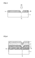
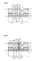
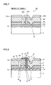
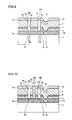
- Figs. 2 to 6 are sectional views for illustrating a process of manufacturing the photovoltaic apparatus according to the first embodiment shown in Fig. 1;
- Fig. 7 is a sectional view showing the structure of a photovoltaic apparatus according to comparative example with respect to the first embodiment of the present invention;
- Fig. 8 is a sectional view showing the structure of a photovoltaic apparatus according to a second embodiment of the present invention;
- Figs. 9 to 11 are sectional views for illustrating a process of manufacturing the photovoltaic apparatus according to the second embodiment shown in Fig. 7; and
- Fig. 12 is a sectional view showing the structure of a photovoltaic apparatus according to a modification of the first embodiment of the present invention.
- Embodiments of the present invention are now described with reference to the drawings.
- The structure of a
photovoltaic apparatus 1 according to a first embodiment of the present invention is described with reference to Fig. 1. - As shown in Fig. 1, the
photovoltaic apparatus 1 according to the first embodiment comprises asubstrate 2,substrate electrodes photoelectric conversion unit 4, anintermediate layer 5, anotherphotoelectric conversion unit 6,back electrodes insulating member 8 and a connectingelectrode 9. Thisphotovoltaic apparatus 1 according to the first embodiment is formed by serially connecting a plurality of units with each other in a direction along the main surface of thesubstrate 2 through the connectingelectrode 9. The structure of thephotovoltaic apparatus 1 is now described in detail. - The
substrate 2, having an insulating surface, consists of translucent glass. Thissubstrate 2 has a thickness of about 1 mm to about 5 mm. Thesubstrate electrodes groove 3c are formed on the upper surface of thesubstrate 2. Thesubstrate electrodes substrate electrodes groove 3c is an example of the "first groove" in the present invention. - The
photoelectric conversion unit 4 consisting of a p-i-n amorphous silicon semiconductor is formed on the upper surfaces of thesubstrate electrodes photoelectric conversion unit 4 of the p-i-n amorphous silicon semiconductor is constituted of a p-type hydrogenated amorphous silicon carbide (a-SiC:H) layer having a thickness of about 10 nm to about 20 nm, an i-type hydrogenated amorphous silicon (a-Si:H) layer having a thickness of about 250 nm to about 350 nm and an n-type hydrogenated amorphous silicon layer having a thickness of about 20 nm to about 30 nm. Thephotoelectric conversion unit 4 is formed on the upper surface of thesubstrate electrode 3a to havegrooves groove 3c. Thephotoelectric conversion unit 4 of the amorphous silicon semiconductor is formed for absorbing light of a relatively short wavelength. Thisphotoelectric conversion unit 4 is an example of the "first photoelectric conversion portion" in the present invention. - The
intermediate layer 5 havinggrooves regions photoelectric conversion unit 4. Thisintermediate layer 5 has a thickness of about 10 nm to about 500 nm. Theintermediate layer 5 consists of TCO such as zinc oxide (ZnO) having conductivity with a function of partly reflecting and partly transmitting light incident from the side of thesubstrate 2. Theintermediate layer 5 also has a function of increasing the quantity of light passing through thephotoelectric conversion unit 4 by partly reflecting the light incident from the side of thesubstrate 2. Therefore, an output current of thephotoelectric conversion unit 4 can be increased without increasing the thickness thereof. In other words, the output current of thephotoelectric conversion unit 4 can be increased while suppressing photo-deterioration remarkably increased in response to the thickness of thephotoelectric conversion unit 4 of the amorphous silicon semiconductor. Thus, the output currents of thephotoelectric conversion units - The
photoelectric conversion unit 6 of a p-i-n microcrystalline siliconsemiconductor having grooves grooves intermediate layer 5. Thisphotoelectric conversion unit 6 of the p-i-n microcrystalline silicon semiconductor is constituted of a p-type hydrogenated microcrystalline silicon (µc-Si:H) layer having a thickness of about 10 nm to about 20 nm, an i-type hydrogenated microcrystalline silicon layer having a thickness of about 1500 nm to about 2000 nm and an n-type hydrogenated microcrystalline silicon layer having a thickness of about 20 nm to about 30 nm. Thephotoelectric conversion unit 6 of the p-i-n microcrystalline silicon semiconductor is formed for absorbing light of a relatively long wavelength. Thephotoelectric conversion unit 6 is an example of the "second photoelectric conversion portion" in the present invention. - The
back electrodes groove 7d formed on a region corresponding to thegroove 6b are formed on the upper surface of thephotoelectric conversion unit 6. Theback electrode 7b hasgrooves grooves back electrodes back electrodes substrate 2 to reach theback electrodes photoelectric conversion units back electrodes - According to the first embodiment, the
grooves groove 20a for electrically isolating theback electrodes grooves groove 20b for electrically isolating portions of theintermediate layer 5 from each other. Further, thegrooves groove 20c for electrically connecting theback electrode 7b and thesubstrate electrode 3a with each other. Thus, thegrooves back electrodes photoelectric conversion unit 6, theintermediate layer 5 and thephotoelectric conversion unit 4 and expose the surface of thesubstrate electrode 3a. Thegrooves - According to the first embodiment, the insulating
member 8 consists of epoxy resin containing aluminum oxide (Al2O3) particles, and is so embedded as to fill up thegroove 20b. In other words, the insulatingmember 8 is so embedded as to electrically insulate portions of thegroove 5c of theintermediate layer 5 located closer to thegrooves member 8 is so provided as to protrude upward beyond the upper surface of theback electrode 7b. The insulatingmember 8 is an example of the "first insulating member" in the present invention. - According to the first embodiment, the connecting
electrode 9 consists of conductive paste (silver paste). This connectingelectrode 9 is embedded in thegroove 20c to come into contact with the surface of thesubstrate electrode 3a exposed in thegroove 20c, and formed to be electrically connected to the upper surface of a region of theback electrode 7b of the adjacent unit located between thegrooves member 8. Thus, thesubstrate electrode 3a and theback electrode 7b of the adjacent unit are serially connected with each other. The connectingelectrode 9 is an example of the "conductive member" in the present invention. - A process of manufacturing the
photovoltaic apparatus 1 according to the first embodiment of the present invention is now described with reference to Figs. 1 to 6. - As shown in Fig. 2, a
substrate electrode 3 of tin oxide having a thickness of about 800 nm is formed on the insulating upper surface of thesubstrate 2 by thermal CVD (chemical vapor deposition). - As shown in Fig. 3, the
groove 3c is formed by scanning thesubstrate electrode 3 with a fundamental wave LB1 of an Nd:YAG laser having a wavelength of about 1064 nm, an oscillation frequency of about 20 kHz and average power of about 14.0 W from above. Thus, thesubstrate electrode 3 is separated into thesubstrate electrodes groove 3c. - As shown in Fig. 4, the
photoelectric conversion unit 4 of the amorphous silicon semiconductor is formed by successively forming the p-type hydrogenated amorphous silicon carbide layer having the thickness of about 10 nm to about 20 nm, the i-type hydrogenated amorphous silicon layer having the thickness of about 250 nm to about 350 nm and the n-type hydrogenated amorphous silicon layer having the thickness of about 20 nm to about 30 nm on the upper surfaces of thesubstrate electrodes intermediate layer 5 of zinc oxide having the thickness of about 10 nm to about 500 nm is formed on the upper surface of thephotoelectric conversion unit 4 by sputtering. Then, thephotoelectric conversion unit 6 of the microcrystalline silicon semiconductor is formed by successively forming the p-type hydrogenated microcrystalline silicon layer having the thickness of about 10 nm to about 20 nm, the i-type hydrogenated microcrystalline silicon layer having the thickness of about 1500 nm to about 2000 nm and the n-type hydrogenated microcrystalline silicon layer having the thickness of about 20 nm to about 30 nm on the upper surface of theintermediate layer 5 by plasma CVD. - Thereafter the
back electrode 7, having the thickness of about 200 nm to about 400 nm, of the metal material mainly composed of silver is formed on the upper surface of thephotoelectric conversion unit 6 by sputtering. - According to the first embodiment, the
photoelectric conversion unit 4, theintermediate layer 5, thephotoelectric conversion unit 6 and theback electrode 7 are so continuously formed that the surfaces of thephotoelectric conversion unit 4, theintermediate layer 5 and thephotoelectric conversion unit 6 are not exposed to the atmosphere. - As shown in Fig. 5, the
groove 20a constituted of thegrooves groove 20b constituted of thegrooves groove 20c constituted of thegrooves groove 3c by scanning thephotoelectric conversion unit 4, theintermediate layer 5, thephotoelectric conversion unit 6 and theback electrode 7 with second harmonics LB2 of an Nd:YAG laser having a wavelength of about 532 nm, an oscillation frequency of about 12 kHz and average power of about 230 mW from the side of thesubstrate 2. Thus, theback electrode 7 is separated into theback electrodes groove 20a. - As shown in Fig. 6, the insulating
member 8 of epoxy resin containing aluminum oxide particles is applied by screen printing, to fill up thegroove 20b and extend onto theback electrode 7b. Thereafter the connectingelectrode 9 is applied by screen printing, to fill up thegroove 20c and be electrically connected to theback electrode 7b across the insulatingmember 8, as shown in Fig. 1. - According to the first embodiment, as hereinabove described, the
photovoltaic apparatus 1 is provided with thegroove 20b so formed as to cut theintermediate layer 5 on the region located between thegroove 3c for electrically isolating thesubstrate electrodes groove 20a for electrically isolating theback electrodes member 8 embedded in thegroove 20b, so that the insulatingmember 8 can electrically insulate the portions of theintermediate layer 5 closer to thegrooves groove 20b respectively from each other. Thephotovoltaic apparatus 1 is further provided with thegroove 20c on the region located between thegroove 20a for electrically isolating theback electrodes groove 20b filled up with the insulatingmember 8 and the connectingelectrode 9 electrically connected to the surface of thesubstrate electrode 3a exposed in thegroove 20c and electrically connected to theback electrode 7b of the adjacent unit across the insulatingmember 8, so that the connectingelectrode 9, electrically insulated from the portion of theintermediate layer 5 closer to thegroove 3c with respect to thegroove 20b by the aforementioned insulatingmember 8, can be inhibited from an electrical short circuit with the portion of theintermediate layer 5 closer to thegroove 3c with respect to thegroove 20b. - According to the first embodiment, the connecting
electrode 9 is provided independently of theback electrode 7 so that the manufacturing process of subsequently forming theback electrode 7 after forming the secondphotoelectric conversion unit 6 and thereafter forming thegroove 20c while forming the connectingmember 9 in thisgroove 20c can be employed, whereby the surface of thephotoelectric conversion unit 6, to be most inhibited from contamination in the process of manufacturing thephotovoltaic apparatus 1, can be prevented from exposure to the atmosphere. - An experiment conducted for confirming the aforementioned effects of the first embodiment is now described. In this confirmatory experiment,
photovoltaic apparatuses - First, the
photovoltaic apparatus 1 according to Example 1 was prepared as shown in Fig. 1, through the manufacturing process employed in the first embodiment. Thephotovoltaic apparatus 101 according to comparative example 1 was prepared to have a structure shown in Fig. 7. At this time, aphotoelectric conversion unit 104, anintermediate layer 105, anotherphotoelectric conversion unit 106 andback electrodes photovoltaic apparatus 101 according to comparative example 1 were so formed as to have the same thicknesses and compositions as those of aphotoelectric conversion unit 4, anintermediate layer 5, anotherphotoelectric conversion unit 6 andback electrodes photovoltaic apparatus 1 according to Example 1 respectively. Further, thephotovoltaic apparatus 101 according to comparative example 1 was formed withonly grooves grooves grooves photovoltaic apparatus 1 according to Example 1 respectively. According to comparative example 1, theback electrode 107b was directly embedded in thegroove 120c, to be electrically connected to asubstrate electrode 3a. - As to the
photovoltaic apparatuses photovoltaic apparatus 101. Table 1 shows the results.Table 1 Open Circuit Voltage Short Circuit Voltage Fill Factor Maximum Power Conversion Efficiency Example 1 1.00 1.04 1.01 1.05 1.05 Comparative Example 1 1.00 1.00 1.00 1.00 1.00 - Referring to Table 1, it has been proved that the open circuit voltage of the
photovoltaic apparatus 1 according to Example 1 is identical to that of thephotovoltaic apparatus 101 according to comparative example 1. It has also been proved that the short circuit current and the fill factor of thephotovoltaic apparatus 1 according to Example 1 are improved by 4 % and 1 % with respect to those of thephotovoltaic apparatus 101 according to comparative example 1 respectively. It has further been proved that the maximum power and the conversion efficiency of thephotovoltaic apparatus 1 according to Example 1 are improved by 5 % and 5 % with respect to those of thephotovoltaic apparatus 101 according to comparative example 1 respectively. - The aforementioned results have conceivably been obtained for the following reasons: In the
photovoltaic apparatus 1 according to Example 1 shown in Fig. 1, an insulatingmember 8 electrically isolates a connectingelectrode 9 from a portion of theintermediate layer 5 closer to agroove 3c with respect to thegroove 20b for inhibiting the connectingelectrode 9 from an electrical short circuit with the portion of theintermediate layer 5 closer to thegroove 3c with respect to thegroove 20b, thereby conceivably improving the conversion efficiency. In thephotovoltaic apparatus 101 according to comparative example 1 shown in Fig. 7, on the other hand, theback electrode 107b embedded in thegroove 120c is in contact with theintermediate layer 5 in thisgroove 120c to cause an electrical short circuit with theintermediate layer 105, conceivably resulting in reduction of the conversion efficiency. - Referring to Fig. 8, a
silicon melt 22 and a connectingelectrode 23 electrically connect asubstrate electrode 3a and aback electrode 7b with each other in aphotovoltaic apparatus 21 according to a second embodiment of the present invention, dissimilarly to the aforementioned first embodiment. - As shown in Fig. 8, the
silicon melt 22 is formed in a region located betweengrooves photoelectric conversion unit 4, anintermediate layer 5, anotherphotoelectric conversion unit 6 and theback electrode 7b in thephotovoltaic apparatus 21 according to the second embodiment. Thissilicon melt 22 has conductivity, and is electrically connected to thesubstrate electrode 3a. Thesilicon melt 22 is an example of the "melt portion" or the "conductive member" in the present invention. - According to the second embodiment, the connecting
electrode 23 is electrically connected with thesilicon melt 22, and electrically connected to anotherback electrode 7b across an insulatingmember 8 embedded in thegroove 20b. The connectingelectrode 23 is an example of the "connecting portion" or the "conductive member" in the present invention. - A process of manufacturing the
photovoltaic apparatus 21 according to the second embodiment of the present invention is now described with reference to Figs. 8 to 11. Steps up to formation of aback electrode 7 are similar to those for thephotovoltaic apparatus 1 according to the first embodiment shown in Figs. 2 to 4. - According to the second embodiment, the
groove 20a constituted ofgrooves groove 20b constituted ofgrooves groove 3c by scanning thephotoelectric conversion unit 4, theintermediate layer 5, thephotoelectric conversion unit 6 and theback electrode 7 with second harmonics LB3 of an Nd:YAG laser having a wavelength of about 532 nm, an oscillation frequency of about 12 kHz and average power of about 230 mW from the side of asubstrate 2, as shown in Fig. 9. Thus, theback electrode 7 is separated into theback electrodes groove 20a. - As shown in Fig. 10, the
photoelectric conversion unit 4, theintermediate layer 5, thephotoelectric conversion unit 6 and theback electrode 7b are scanned with a fundamental wave LB4 of an Nd:YAG laser having a wavelength of about 1064 nm, an oscillation frequency of about 20 kHz and average power of about 8 W on the region located between thegrooves back electrode 7b to be partially melted, thereby forming thesilicon melt 22. Thereafter the insulatingmember 8 of epoxy resin containing aluminum oxide particles is applied by screen printing to fill up thegroove 20b and extend onto theback electrode 7b, as shown in Fig. 11. - Then, the connecting
electrode 23 of silver paste is applied by screen printing, to come into contact with the surface of thesilicon melt 22 and be electrically connected to theback electrode 7b across the insulatingmember 8. - According to the second embodiment, as hereinabove described, the
silicon melt 22 and the connectingelectrode 23 electrically connect thesubstrate electrode 3a and theback electrode 7b with each other, whereby the quantity of the material for the connectingelectrode 23 of silver paste can be reduced as compared with the first embodiment connecting thesubstrate electrode 3a and theback electrode 7b with each other only through the connectingelectrode 9. - The remaining effects of the second embodiment are similar to those of the aforementioned first embodiment.
- Although the present invention has been described and illustrated in detail, it is clearly understood that the same is by way of illustration and example only and is not to be taken by way of limitation, the spirit and scope of the present invention being limited only by the terms of the appended claims.
- For example, while the
groove 7d separates theback electrodes groove 7d may separate backelectrodes member 10 may fill up agroove 20a constituted ofgrooves groove 20a when a connectingelectrode member 10 is an example of the "second insulating member" in the present invention. - While the
groove 20b constituted of thegrooves member 8 in each of the aforementioned first and second embodiments, the present invention is not restricted to this but at least thegroove 5c may be formed to be filled up with the insulatingmember 8 for covering at least a cut portion of thegroove 5c.
Claims (20)
- A photovoltaic apparatus comprising:a substrate (2) having an insulating surface;a first substrate electrode (3a) and a second substrate electrode (3b) formed on said insulating surface of said substrate and isolated from each other by a first groove (3c);a first photoelectric conversion portion (4) so formed as to cover said first substrate electrode and said second substrate electrode;a second photoelectric conversion portion (6) formed on the surface of said first photoelectric conversion portion through a conductive intermediate layer (5);a first back electrode (7a) and a second back electrode (7b), formed on the surface of said second photoelectric conversion portion, corresponding to said first substrate electrode and said second substrate electrode respectively;a second groove (20a) for electrically isolating said first back electrode and said second back electrode from each other;a third groove (20b) formed on a region located between said first groove and said second groove to cut at least said intermediate layer from the upper surface of said second back electrode;a first insulating member (8) embedded in said third groove to cover at least a cut portion of said intermediate layer; anda conductive member (9) electrically connected to said first substrate electrode on a region located between said second groove and said third groove and electrically connected to said second back electrode across said third groove.
- The photovoltaic apparatus according to claim 1, further comprising a fourth groove (20c) formed on said region located between said second groove and said third groove to pass through said second back electrode, said second photoelectric conversion portion, said intermediate layer and said first photoelectric conversion portion and expose the surface of said first substrate electrode, whereinsaid conductive member is embedded in said fourth groove to come into contact with the surface of said first substrate electrode exposed in said fourth groove and formed to be electrically connected to said second back electrode across said first insulating member embedded in said third groove.
- The photovoltaic apparatus according to claim 1, whereinsaid conductive member includes a conductive melt portion (1) obtained by partially melting said second back electrode, said second photoelectric conversion portion, said intermediate layer and said first photoelectric conversion portion and electrically connected to said first substrate electrode and a connecting portion (23) formed to be electrically connected to said melt portion and to be electrically connected to said second back electrode across said first insulating member embedded in said third groove on said region located between said second groove and said third groove.
- The photovoltaic apparatus according to claim 1, whereinsaid first insulating member fills up said third groove.
- The photovoltaic apparatus according to claim 4, whereinthe upper surface of said first insulating member is so formed as to project upward beyond the upper surface of said second back electrode.
- The photovoltaic apparatus according to claim 1, whereinsaid conductive member is so formed as to come into contact with the surface of a region of said second back electrode located between said first groove and said third groove.
- The photovoltaic apparatus according to claim 1, whereinsaid second groove is so formed as to pass through said second back electrode, said second photoelectric conversion portion, said intermediate layer and said first photoelectric conversion portion and expose the surface of said first substrate electrode.
- The photovoltaic apparatus according to claim 1, whereinsaid third groove is so formed as to pass through said second back electrode, said second photoelectric conversion portion, said intermediate layer and said first photoelectric conversion portion and expose the surface of said first substrate electrode.
- The photovoltaic apparatus according to claim 1, further comprising a second insulating member (1) embedded in said second groove.
- The photovoltaic apparatus according to claim 9, whereinsaid second insulating member fills up said second groove.
- The photovoltaic apparatus according to claim 1, whereinsaid intermediate layer has a function of partly reflecting and partly transmitting light incident from the side of said substrate.
- A method of manufacturing a photovoltaic apparatus, comprising steps of:forming a substrate electrode (3) on an insulating surface of a substrate (2) having said insulating surface;forming a first substrate electrode (3a) and a second substrate electrode (3b) isolated from each other by a first groove by forming said first groove (3c) on said substrate electrode;forming a first photoelectric conversion portion (4) to cover said first substrate electrode and said second substrate electrode;forming a second photoelectric conversion portion (6) on the surface of said first photoelectric conversion portion through a conductive intermediate layer (5);forming a back electrode (7) on the surface of said second photoelectric conversion portion;thereafter forming a second groove (20a) for separating said back electrode into a first back electrode (7a) and a second back electrode (7b) while forming a third groove (20b) on a region located between said first groove and said second groove to pass through at least said intermediate layer from the upper surface of said second back electrode;forming a first insulating member (8) in said third groove to cover at least a cut portion of said intermediate layer; andforming a conductive member (9) electrically connected to said first substrate electrode on a region located between said second groove and said third groove and electrically connected to said second back electrode across said third groove.
- The method of manufacturing a photovoltaic apparatus according to claim 12, further comprising a step of forming a fourth groove (20c) on said region located between said second groove and said third groove to pass through said second back electrode, said second photovoltaic conversion portion, said intermediate layer and said first photoelectric conversion portion and expose the surface of said first substrate electrode, whereinsaid step of forming said conductive member includes a step of embedding said conductive member in said fourth groove to come into contact with the surface of said first substrate electrode exposed in said fourth groove while electrically connecting said conductive member to said second back electrode across said first insulating member embedded in said third groove.
- The method of manufacturing a photovoltaic apparatus according to claim 13, whereinsaid step of forming said second groove and said third groove is carried out substantially simultaneously with said step of forming said fourth groove.
- The method of manufacturing a photovoltaic apparatus according to claim 12, whereinsaid step of forming said conductive member includes a step of forming said conductive member to come into contact with a region of said second back electrode located between said first groove and said third groove.
- The method of manufacturing a photovoltaic apparatus according to claim 12, whereinsaid step of forming said conductive member includes steps of:forming a conductive melt portion (3a) electrically connected to said first substrate electrode by partially melting said second back electrode, said second photoelectric conversion portion, said intermediate layer and said first photoelectric conversion portion on said region located between said second groove and said third groove, andforming a connecting portion (3a) to be electrically connected to said melt portion and to be electrically connected to said second back electrode across said first insulating member embedded in said third groove.
- The method of manufacturing a photovoltaic apparatus according to claim 12, whereinsaid step of forming said third groove includes a step of forming said third groove to pass through said second back electrode, said second photoelectric conversion portion, said intermediate layer and said first photoelectric conversion portion and expose the surface of said first substrate electrode.
- The method of manufacturing a photovoltaic apparatus according to claim 17, whereinsaid step of forming said first insulating member includes a step of filling said third groove with said first insulating member.
- The method of manufacturing a photovoltaic apparatus according to claim 12, whereinsaid step of forming said second groove includes a step of forming said second groove to pass through said second back electrode, said second photoelectric conversion portion, said intermediate layer and said first photoelectric conversion portion and expose the surface of said first substrate electrode.
- The method of manufacturing a photovoltaic apparatus according to claim 19, further comprising a step of filling said second groove with a second insulating member (3a).
Applications Claiming Priority (1)
| Application Number | Priority Date | Filing Date | Title |
|---|---|---|---|
| JP2006046083A JP5081389B2 (en) | 2006-02-23 | 2006-02-23 | Method for manufacturing photovoltaic device |
Publications (2)
| Publication Number | Publication Date |
|---|---|
| EP1826830A2 true EP1826830A2 (en) | 2007-08-29 |
| EP1826830A3 EP1826830A3 (en) | 2010-02-24 |
Family
ID=38134845
Family Applications (1)
| Application Number | Title | Priority Date | Filing Date |
|---|---|---|---|
| EP07250625A Withdrawn EP1826830A3 (en) | 2006-02-23 | 2007-02-15 | Photovoltaic apparatus and method of manufacturing the same |
Country Status (4)
| Country | Link |
|---|---|
| US (1) | US8207441B2 (en) |
| EP (1) | EP1826830A3 (en) |
| JP (1) | JP5081389B2 (en) |
| CN (2) | CN101026174B (en) |
Cited By (2)
| Publication number | Priority date | Publication date | Assignee | Title |
|---|---|---|---|---|
| EP2083445A1 (en) * | 2008-01-26 | 2009-07-29 | SCHOTT Solar GmbH | Method of production of a photovoltaic modul |
| EP2717327A4 (en) * | 2011-05-23 | 2014-12-17 | Byung Kuk Kim | SOLAR CELL, AND MANUFACTURING METHOD THEREOF |
Families Citing this family (15)
| Publication number | Priority date | Publication date | Assignee | Title |
|---|---|---|---|---|
| JP4425296B2 (en) | 2007-07-09 | 2010-03-03 | 三洋電機株式会社 | Photovoltaic device |
| EP2187449A1 (en) * | 2007-08-14 | 2010-05-19 | Mitsubishi Heavy Industries, Ltd. | Photoelectric conversion device, and its manufacturing method |
| US20110220189A1 (en) * | 2007-09-18 | 2011-09-15 | Mitsubishi Electric Corporation | Thin film solar cell device and method of manufacturing the same |
| JP4785827B2 (en) * | 2007-12-27 | 2011-10-05 | 三洋電機株式会社 | Solar cell module and manufacturing method thereof |
| CN102047440A (en) * | 2008-07-04 | 2011-05-04 | 株式会社爱发科 | Manufacturing method of solar battery unit and solar battery unit |
| DE102009022318A1 (en) * | 2009-05-22 | 2010-12-23 | Schott Solar Ag | Method for producing a photovoltaic module |
| KR101028971B1 (en) * | 2009-05-26 | 2011-04-19 | 한국과학기술원 | Integrated thin film solar cell and manufacturing method thereof |
| KR101173418B1 (en) * | 2011-07-29 | 2012-08-10 | 엘지이노텍 주식회사 | Solar cell and method of fabricating the same |
| KR101283072B1 (en) * | 2011-10-18 | 2013-07-05 | 엘지이노텍 주식회사 | Solar cell apparatus and method of fabricating the same |
| JP2013149697A (en) * | 2012-01-18 | 2013-08-01 | Fujifilm Corp | Integrated soar cell manufacturing method |
| US20130229777A1 (en) * | 2012-03-01 | 2013-09-05 | Infineon Technologies Ag | Chip arrangements and methods for forming a chip arrangement |
| KR101393743B1 (en) * | 2012-06-28 | 2014-05-13 | 엘지이노텍 주식회사 | Solar cell and method of fabricating the same |
| TWM545367U (en) * | 2017-02-24 | 2017-07-11 | 位元奈米科技股份有限公司 | Photovoltaic cell device, photovoltaic cell and photovoltaic module |
| WO2020188777A1 (en) * | 2019-03-19 | 2020-09-24 | 株式会社 東芝 | Photoelectric conversion element and method for manufacturing photoelectric conversion element |
| EP4601018A4 (en) * | 2022-11-30 | 2025-11-12 | Contemporary Amperex Technology Hong Kong Ltd | Thin-layer solar cell and electrical device |
Citations (1)
| Publication number | Priority date | Publication date | Assignee | Title |
|---|---|---|---|---|
| JP2002118273A (en) | 2000-10-05 | 2002-04-19 | Kanegafuchi Chem Ind Co Ltd | Integrated hybrid thin film photoelectric conversion device |
Family Cites Families (22)
| Publication number | Priority date | Publication date | Assignee | Title |
|---|---|---|---|---|
| US4110122A (en) * | 1976-05-26 | 1978-08-29 | Massachusetts Institute Of Technology | High-intensity, solid-state-solar cell device |
| JPS59201471A (en) * | 1983-04-29 | 1984-11-15 | Semiconductor Energy Lab Co Ltd | Photoelectric conversion semiconductor device |
| US4697041A (en) | 1985-02-15 | 1987-09-29 | Teijin Limited | Integrated solar cells |
| JPS61214483A (en) | 1985-03-19 | 1986-09-24 | Teijin Ltd | Manufacture of integrated type solar cell |
| US4675467A (en) * | 1986-04-05 | 1987-06-23 | Chronar Corp. | Directed energy conversion of semiconductor materials |
| JPH07114292B2 (en) * | 1986-12-22 | 1995-12-06 | 鐘淵化学工業株式会社 | Semiconductor device and manufacturing method thereof |
| DE4420434A1 (en) * | 1994-06-10 | 1995-12-14 | Siemens Ag | Solar modulus prodn. for converting solar light to electricity |
| US6265652B1 (en) | 1995-06-15 | 2001-07-24 | Kanegafuchi Kagaku Kogyo Kabushiki Kabushiki Kaisha | Integrated thin-film solar battery and method of manufacturing the same |
| JP3017422B2 (en) * | 1995-09-11 | 2000-03-06 | キヤノン株式会社 | Photovoltaic element array and manufacturing method thereof |
| JP3755048B2 (en) * | 1995-10-30 | 2006-03-15 | 株式会社カネカ | Integrated thin film tandem solar cell and manufacturing method thereof |
| JP2000058886A (en) * | 1998-08-14 | 2000-02-25 | Mitsubishi Heavy Ind Ltd | Solar cell module and method of manufacturing the same |
| JP4441048B2 (en) * | 2000-03-23 | 2010-03-31 | 株式会社カネカ | Manufacturing method of integrated thin film solar cell |
| US6632993B2 (en) * | 2000-10-05 | 2003-10-14 | Kaneka Corporation | Photovoltaic module |
| JP2002261308A (en) | 2001-03-01 | 2002-09-13 | Kanegafuchi Chem Ind Co Ltd | Thin-film photoelectric conversion module |
| JP4201241B2 (en) | 2001-05-17 | 2008-12-24 | 株式会社カネカ | Method for manufacturing integrated thin film photoelectric conversion module |
| JP2003273383A (en) | 2002-03-15 | 2003-09-26 | Sharp Corp | Solar cell element and manufacturing method therefor |
| JP2004095661A (en) | 2002-08-29 | 2004-03-25 | Sanyo Electric Co Ltd | Photoelectric converting device and its manufacturing method |
| JP4365636B2 (en) * | 2003-07-15 | 2009-11-18 | 京セラ株式会社 | Integrated photoelectric conversion device |
| JP2005093939A (en) * | 2003-09-19 | 2005-04-07 | Mitsubishi Heavy Ind Ltd | Integrated tandem connection solar cell and manufacturing method of integrated tandem connection solar cell |
| JP2005101384A (en) * | 2003-09-26 | 2005-04-14 | Sanyo Electric Co Ltd | Photovoltaic device and manufacturing method thereof |
| JP2006013403A (en) | 2004-06-29 | 2006-01-12 | Sanyo Electric Co Ltd | SOLAR CELL, SOLAR CELL MODULE, ITS MANUFACTURING METHOD, AND ITS REPAIR METHOD |
| US7235736B1 (en) | 2006-03-18 | 2007-06-26 | Solyndra, Inc. | Monolithic integration of cylindrical solar cells |
-
2006
- 2006-02-23 JP JP2006046083A patent/JP5081389B2/en not_active Expired - Fee Related
-
2007
- 2007-02-14 US US11/705,770 patent/US8207441B2/en not_active Expired - Fee Related
- 2007-02-15 CN CN2007100788236A patent/CN101026174B/en not_active Expired - Fee Related
- 2007-02-15 EP EP07250625A patent/EP1826830A3/en not_active Withdrawn
- 2007-02-15 CN CN2010100033454A patent/CN101794794B/en not_active Expired - Fee Related
Patent Citations (1)
| Publication number | Priority date | Publication date | Assignee | Title |
|---|---|---|---|---|
| JP2002118273A (en) | 2000-10-05 | 2002-04-19 | Kanegafuchi Chem Ind Co Ltd | Integrated hybrid thin film photoelectric conversion device |
Cited By (2)
| Publication number | Priority date | Publication date | Assignee | Title |
|---|---|---|---|---|
| EP2083445A1 (en) * | 2008-01-26 | 2009-07-29 | SCHOTT Solar GmbH | Method of production of a photovoltaic modul |
| EP2717327A4 (en) * | 2011-05-23 | 2014-12-17 | Byung Kuk Kim | SOLAR CELL, AND MANUFACTURING METHOD THEREOF |
Also Published As
| Publication number | Publication date |
|---|---|
| JP2007227577A (en) | 2007-09-06 |
| CN101794794A (en) | 2010-08-04 |
| US8207441B2 (en) | 2012-06-26 |
| CN101026174A (en) | 2007-08-29 |
| CN101794794B (en) | 2011-12-28 |
| US20070193619A1 (en) | 2007-08-23 |
| CN101026174B (en) | 2010-05-26 |
| EP1826830A3 (en) | 2010-02-24 |
| JP5081389B2 (en) | 2012-11-28 |
Similar Documents
| Publication | Publication Date | Title |
|---|---|---|
| US8207441B2 (en) | Photovoltaic apparatus and method of manufacturing the same | |
| EP1826828A2 (en) | Photovoltaic apparatus | |
| US8362354B2 (en) | Photovoltaic apparatus and method of manufacturing the same | |
| EP1727211B1 (en) | Method of fabricating a thin-film solar cell, and thin-film solar cell | |
| EP0631328A1 (en) | Solar cell module having heat-fused portion to improve moisture resistance | |
| US20150027517A1 (en) | Method and structure for tiling industrial thin-film solar devices | |
| KR101168811B1 (en) | Thin film solar battery module manufacturing method and thin film solar battery module | |
| JP5220134B2 (en) | Photoelectric conversion cell and photoelectric conversion module | |
| CA2668103A1 (en) | Front electrode with thin metal film layer and high work-function buffer layer for use in photovoltaic device and method of making same | |
| CN101952965B (en) | Method for providing a series connection in a solar cell system | |
| US20120199173A1 (en) | Interconnection Schemes for Photovoltaic Cells | |
| US5236516A (en) | Photovoltaic apparatus | |
| JP3243229B2 (en) | Solar cell module | |
| JP2009283982A (en) | Method of manufacturing thin-film solar cell module | |
| JP2010093309A (en) | Method of manufacturing thin-film solar cell module | |
| JPH11103079A (en) | Manufacturing method of integrated photovoltaic device | |
| JP2010093308A (en) | Method of manufacturing thin-film solar cell module | |
| US20110023933A1 (en) | Interconnection Schemes for Photovoltaic Cells | |
| JP2001111079A (en) | Method for manufacturing photoelectric conversion device | |
| EP4046204A1 (en) | Photovoltaic devices and methods of making |
Legal Events
| Date | Code | Title | Description |
|---|---|---|---|
| PUAI | Public reference made under article 153(3) epc to a published international application that has entered the european phase |
Free format text: ORIGINAL CODE: 0009012 |
|
| AK | Designated contracting states |
Kind code of ref document: A2 Designated state(s): AT BE BG CH CY CZ DE DK EE ES FI FR GB GR HU IE IS IT LI LT LU LV MC NL PL PT RO SE SI SK TR |
|
| AX | Request for extension of the european patent |
Extension state: AL BA HR MK YU |
|
| PUAL | Search report despatched |
Free format text: ORIGINAL CODE: 0009013 |
|
| AK | Designated contracting states |
Kind code of ref document: A3 Designated state(s): AT BE BG CH CY CZ DE DK EE ES FI FR GB GR HU IE IS IT LI LT LU LV MC NL PL PT RO SE SI SK TR |
|
| AX | Request for extension of the european patent |
Extension state: AL BA HR MK RS |
|
| RIC1 | Information provided on ipc code assigned before grant |
Ipc: H01L 31/20 20060101ALI20100120BHEP Ipc: H01L 27/142 20060101ALI20100120BHEP Ipc: H01L 31/075 20060101AFI20100120BHEP |
|
| AKY | No designation fees paid | ||
| 17P | Request for examination filed |
Effective date: 20100818 |
|
| RBV | Designated contracting states (corrected) |
Designated state(s): AT BE BG CH CY CZ DE DK EE ES FI FR GB GR HU IE IS IT LI LT LU LV MC NL PL PT RO SE SI SK TR |
|
| REG | Reference to a national code |
Ref country code: DE Ref legal event code: 8566 |
|
| 17Q | First examination report despatched |
Effective date: 20110922 |
|
| GRAP | Despatch of communication of intention to grant a patent |
Free format text: ORIGINAL CODE: EPIDOSNIGR1 |
|
| RIC1 | Information provided on ipc code assigned before grant |
Ipc: H01L 27/142 20060101ALI20120123BHEP Ipc: H01L 31/20 20060101ALI20120123BHEP Ipc: H01L 31/076 20120101AFI20120123BHEP |
|
| RTI1 | Title (correction) |
Free format text: PHOTOVOLTAIC DEVICE AND METHOD OF MANUFACTURING THE SAME |
|
| STAA | Information on the status of an ep patent application or granted ep patent |
Free format text: STATUS: THE APPLICATION IS DEEMED TO BE WITHDRAWN |
|
| 18D | Application deemed to be withdrawn |
Effective date: 20120613 |