EP1826769A2 - Speichermodul - Google Patents
Speichermodul Download PDFInfo
- Publication number
- EP1826769A2 EP1826769A2 EP07250166A EP07250166A EP1826769A2 EP 1826769 A2 EP1826769 A2 EP 1826769A2 EP 07250166 A EP07250166 A EP 07250166A EP 07250166 A EP07250166 A EP 07250166A EP 1826769 A2 EP1826769 A2 EP 1826769A2
- Authority
- EP
- European Patent Office
- Prior art keywords
- phase
- clock
- clock signal
- memory module
- dimm
- Prior art date
- Legal status (The legal status is an assumption and is not a legal conclusion. Google has not performed a legal analysis and makes no representation as to the accuracy of the status listed.)
- Withdrawn
Links
Images





Classifications
-
- G—PHYSICS
- G11—INFORMATION STORAGE
- G11C—STATIC STORES
- G11C11/00—Digital stores characterised by the use of particular electric or magnetic storage elements; Storage elements therefor
- G11C11/21—Digital stores characterised by the use of particular electric or magnetic storage elements; Storage elements therefor using electric elements
- G11C11/34—Digital stores characterised by the use of particular electric or magnetic storage elements; Storage elements therefor using electric elements using semiconductor devices
- G11C11/40—Digital stores characterised by the use of particular electric or magnetic storage elements; Storage elements therefor using electric elements using semiconductor devices using transistors
- G11C11/401—Digital stores characterised by the use of particular electric or magnetic storage elements; Storage elements therefor using electric elements using semiconductor devices using transistors forming cells needing refreshing or charge regeneration, i.e. dynamic cells
- G11C11/4063—Auxiliary circuits, e.g. for addressing, decoding, driving, writing, sensing or timing
- G11C11/407—Auxiliary circuits, e.g. for addressing, decoding, driving, writing, sensing or timing for memory cells of the field-effect type
- G11C11/4076—Timing circuits
-
- G—PHYSICS
- G11—INFORMATION STORAGE
- G11C—STATIC STORES
- G11C29/00—Checking stores for correct operation ; Subsequent repair; Testing stores during standby or offline operation
- G11C29/02—Detection or location of defective auxiliary circuits, e.g. defective refresh counters
-
- G—PHYSICS
- G11—INFORMATION STORAGE
- G11C—STATIC STORES
- G11C29/00—Checking stores for correct operation ; Subsequent repair; Testing stores during standby or offline operation
- G11C29/02—Detection or location of defective auxiliary circuits, e.g. defective refresh counters
- G11C29/022—Detection or location of defective auxiliary circuits, e.g. defective refresh counters in I/O circuitry
-
- G—PHYSICS
- G11—INFORMATION STORAGE
- G11C—STATIC STORES
- G11C29/00—Checking stores for correct operation ; Subsequent repair; Testing stores during standby or offline operation
- G11C29/02—Detection or location of defective auxiliary circuits, e.g. defective refresh counters
- G11C29/028—Detection or location of defective auxiliary circuits, e.g. defective refresh counters with adaption or trimming of parameters
-
- G—PHYSICS
- G11—INFORMATION STORAGE
- G11C—STATIC STORES
- G11C29/00—Checking stores for correct operation ; Subsequent repair; Testing stores during standby or offline operation
- G11C29/04—Detection or location of defective memory elements, e.g. cell constructio details, timing of test signals
- G11C29/50—Marginal testing, e.g. race, voltage or current testing
- G11C29/50008—Marginal testing, e.g. race, voltage or current testing of impedance
-
- G—PHYSICS
- G11—INFORMATION STORAGE
- G11C—STATIC STORES
- G11C29/00—Checking stores for correct operation ; Subsequent repair; Testing stores during standby or offline operation
- G11C29/04—Detection or location of defective memory elements, e.g. cell constructio details, timing of test signals
- G11C29/50—Marginal testing, e.g. race, voltage or current testing
- G11C29/50012—Marginal testing, e.g. race, voltage or current testing of timing
-
- G—PHYSICS
- G11—INFORMATION STORAGE
- G11C—STATIC STORES
- G11C5/00—Details of stores covered by group G11C11/00
- G11C5/02—Disposition of storage elements, e.g. in the form of a matrix array
- G11C5/04—Supports for storage elements, e.g. memory modules; Mounting or fixing of storage elements on such supports
-
- G—PHYSICS
- G11—INFORMATION STORAGE
- G11C—STATIC STORES
- G11C7/00—Arrangements for writing information into, or reading information out from, a digital store
- G11C7/22—Read-write [R-W] timing or clocking circuits; Read-write [R-W] control signal generators or management
-
- G—PHYSICS
- G11—INFORMATION STORAGE
- G11C—STATIC STORES
- G11C7/00—Arrangements for writing information into, or reading information out from, a digital store
- G11C7/22—Read-write [R-W] timing or clocking circuits; Read-write [R-W] control signal generators or management
- G11C7/222—Clock generating, synchronizing or distributing circuits within memory device
-
- H—ELECTRICITY
- H03—ELECTRONIC CIRCUITRY
- H03L—AUTOMATIC CONTROL, STARTING, SYNCHRONISATION OR STABILISATION OF GENERATORS OF ELECTRONIC OSCILLATIONS OR PULSES
- H03L7/00—Automatic control of frequency or phase; Synchronisation
- H03L7/06—Automatic control of frequency or phase; Synchronisation using a reference signal applied to a frequency- or phase-locked loop
- H03L7/08—Details of the phase-locked loop
- H03L7/081—Details of the phase-locked loop provided with an additional controlled phase shifter
- H03L7/0812—Details of the phase-locked loop provided with an additional controlled phase shifter and where no voltage or current controlled oscillator is used
-
- G—PHYSICS
- G11—INFORMATION STORAGE
- G11C—STATIC STORES
- G11C2207/00—Indexing scheme relating to arrangements for writing information into, or reading information out from, a digital store
- G11C2207/22—Control and timing of internal memory operations
- G11C2207/2254—Calibration
Definitions
- the present invention relates to a memory module having an array of memory devices, mounted thereon, that operate synchronously with a clock signal.
- SDRAM Serial Dynamic Random Access Memory
- the SDRAM has the characteristic of achieving high access speeds by operating synchronously with the system bus clock, and is often used in the form of a DIMM (Dual In-line Memory Module).
- DIMM Digital In-line Memory Module
- the DIMM is a memory module that has separate independent contacts on either side, the combined number of pins on both sides being, for example, 184, and is capable of transferring data in blocks of 72 bits.
- clock distribution is performed using a PLL (Phase-Locked Loop) circuit mounted on the DIMM; that is, the PLL circuit adjusts the phase of the clock signal input via a terminal of the DIMM, and distributes the phase-adjusted clock signal to the designated terminals of the respective memory devices.
- PLL Phase-Locked Loop
- Such phase adjustment is done, during the development of the DIMM, so that the delay of the clock signal from the terminal of the DIMM to the terminal of each memory device will be zero.
- Japanese Unexamined Patent Publication No. H09-190239 discloses a clock skew adjusting circuit which outputs a clock to a synchronization circuit by compensating for an input delay of the clock from a clock driver, the clock skew adjusting circuit comprising a phase-locked loop which outputs the clock by making an adjustment so that the clock input and the feedback input have a predetermined phase relationship, wherein an inverting circuit for inverting an input signal for output is inserted in a feedback path through which the clock output from the phase-locked loop is fed back to a feedback input.
- Japanese Unexamined Patent Publication No. 2000-163999 discloses a self-timing control circuit which delays a supplied clock and thereby generates a timing clock having a predetermined phase relationship with the supplied clock, the self-timing control circuit comprising a first variable delay circuit to which the supplied clock is input, and which delays the supplied clock by an amount controlled in accordance with the frequency of the supplied clock, and an additional delay circuit which is connected to the first variable delay circuit and which delays the supplied clock by a predetermined amount regardless of the frequency of the supplied clock, wherein the additional delay circuit includes a variable dummy load whose delay amount is variably set, and the delay amount of the variable dummy load is variably set by a programmable memory provided to set the delay amount.
- Japanese Unexamined Patent Publication No. 2001-160000 discloses a memory control integrated circuit which controls SDRAM by receiving a signal from a higher-order device as well as an input clock, the memory control integrated circuit comprising a memory control section, a PLL, and a clock distribution section, wherein the memory control section outputs a signal,for controlling the SDRAM, the PLL receives the input clock and a feedback clock and supplies a clock, synchronized to the input clock and the feedback clock, to the clock distribution section, and the clock distribution section outputs an SDRAM clock to be supplied to the SDRAM, the feedback clock to be input to the PLL, and a read clock for latching data from the SDRAM.
- Japanese Unexamined Patent Publication No. 2001-186017 discloses a PLL circuit comprising an oscillator whose oscillation output frequency is controlled in accordance with a phase comparison result output from a phase comparator, a first low-pass filter to which the oscillator output is input, a buffer which produces an output that matches the result of the comparison between the filter output and a predetermined threshold value, and a control means for controlling the threshold value, wherein the phase comparator outputs the phase difference between the output of the buffer and the input signal to the comparator as the phase comparison result output, and the oscillation output of the oscillator is derived as the output of the PLL circuit.
- the present invention has been devised in view of the above problem, and embodiments thereof may provide a memory module having an array of memory devices mounted thereon that operate synchronously with a clock signal, wherein provisions are made to be able to fine-tune the clock phase in accordance with its use conditions.
- a memory module having an array of memory devices mounted thereon that operate synchronously with a clock signal, comprising: a phase-locked loop circuit which produces an output clock signal adjusted so that the phase of a feedback signal obtained by passing the output clock signal through a feedback loop matches the phase of an input clock signal; and a switching unit which selectively changes a load in the feedback loop in accordance with an external signal.
- the switching unit changes a capacitance in the feedback loop.
- the switching unit changes a resistance value in the feedback loop.
- the switching unit selectively changes the load in the feedback loop in accordance with a value that is set in a register by a controller.
- a memory module having an array of memory devices mounted thereon that operate synchronously with a clock signal, comprising: a phase-locked loop circuit which produces an output clock signal adjusted so that the phase of a feedback signal obtained by passing the output clock signal through a feedback loop matches the phase of an input clock signal; and a unit which, in accordance with an external signal, changes a reference level based on which a phase comparator circuit in the phase-locked loop circuit judges the value of the feedback signal.
- the clock phase can be adjusted, and the reliability of the memory module can be enhanced.
- FIG. 1 shows the general configuration of a DIMM.
- the DIMM 10 shown here comprises a plurality of SDRAM devices 16 and a PLL-based clock driver 20 for distributing a clock signal to them.
- a differential clock signal CLK, /CLK input via a DIMM edge terminal is phase-adjusted by the PLL-based clock driver 20 before being distribution to the respective SDRAM devices 16.
- /CLK is a substitute notation for CLK with a bar over it.
- Each SDRAM device 16 operates synchronously with the supplied clock signal, and outputs differential data DQS, /DQS to a DIMM edge terminal.
- reference numeral 12 indicates a CLK terminal (or /CLK terminal), and 14 a DQS terminal (or /DQS terminal).
- the wiring pattern for the clock signal from the PLL-based clock driver 20 to the respective SDRAM devices 16 is designed so that the wiring length is the same for all the SDRAM devices 16.
- the feedback loop to be provided outside the PLL-based clock driver 20 is designed so that the phase difference of the clock signal between the clock input terminal 22 of the PLL-based clock driver 20 and the clock input terminal 18 of each SDRAM device 16 will be zero. Then, for the delay time tCLKDQS which defines the time from when the clock CLK is applied to the CLK terminal 12 until the memory output data DQS appears at the DQS terminal 14, its minimum value tCLKDQSmin and maximum value tCLKDQSmax are determined as specification values for the DIMM 10.
- FIG. 2 is a circuit diagram showing how the clock is distributed within the DIMM 10. As shown, the differential clock signals CLK and /CLK input from the edge terminal of the DIMM 10 are applied to the input terminals CKI and /CKI of the PLL-based clock driver 20. A resistor and a capacitor are connected in parallel between the CLK line and /CLK line.
- the differential clock signals RCK and /RCK output from the output terminals CKO and /CKO of the PLL-based clock driver 20 are supplied to each SDRAM device 16.
- a termination resistor R is connected between the CKO line and /CKO line.
- the differential data DQS and /DQS output from each SDRAM device 16 are directed to the output edge terminal of the DIMM 10.
- the differential signals output from the feedback output terminals FBO and /FBO of the PLL-based clock driver 20 are directed via the feedback loop to the feedback input terminals FBI and /FBI of the driver 20.
- a resistor 24 and a capacitor 26 are connected in parallel between the two lines forming the feedback loop.
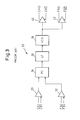
- FIG. 3 is a diagram showing the internal configuration of the PLL-based clock driver 20.
- the differential clock input CKI, /CKI is supplied via a buffer 30 to one input of a phase comparator (PC) 34.
- the differential feedback input FBI, /FBI is supplied via a buffer 32 to the other input of the phase comparator (PC) 34.
- the phase comparator (PC) 34 outputs a voltage proportional to the phase difference between the two inputs, and supplies it to a loop filter (LF) 36.
- LF loop filter
- the loop filter (LF) 36 which is constructed from a low-pass filter, averages the output of the phase comparator (PC) 34 and supplies it to a voltage controlled oscillator (VCO) 38 at the next stage.
- the voltage controlled oscillator (VCO) 38 oscillates at a frequency proportional to the input voltage. Its output is presented as differential output clock signals CKO and /CKO via a buffer 40 and as differential feedback outputs FBO and /FBO via a buffer 42. Actually, a plurality of buffers 40 are provided, but only one such buffer is shown for simplicity of illustration.
- the PLL-based clock driver 20 operates so that the phase of the feedback input FBI, /FBI matches the phase of the clock input CKI, /CKI. Accordingly, the phase of the output clock can be adjusted by varying the length of the feedback loop line and the load (resistor 24 and capacitor 26).
- the length of the feedback loop line and the load are determined so that the phase of the input clock to the PLL-based clock driver 20 matches the phase of the input clock to each SDRAM device 16.
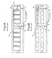
- a difference can also occur depending on how the DIMM is mounted in the host apparatus. For example, when there are four slots 50A, 50B, 50C, and 50D as shown in Figure 5, differences occur in DIMM access time due to differences in the number of slots used, a mixture of DIMMs of different capacities, etc.
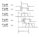
- FIGS 6A, 6B, 6C, 6D, and 6E are timing charts showing the relationships among the input clock CLK to the DIMM 10, the input clock RCK to the SDRAM 16, and the output data DQS from the DIMM 10.
- the phase adjustment is done using the feedback loop so that the phase difference between the input clock CLK to the DIMM and the input clock RCK to the SDRAM becomes zero.
- the rise time of RCK varies within the range of t1 to t2 in relation to the rise time t0 of CLK.
- the timing specification value for the output data DQS from the DIMM is also determined. That is, the rise time of DQS lies within the range of t3 to t4 in relation to the rise time t0 of CLK.
- a phase shift T0 can occur between RCK and CLK, as shown in Figure 6D.
- the rise time of RCK varies within the range of t5 to t6 in relation to the rise time t0 of CLK.
- the rise time of DQS is further shifted and lies within the range of t7 to t8, as shown in Figure 6E.
- the rise time of RCK can eventually vary within the range of t3 to t8 in relation to the rise time t0 of CLK.
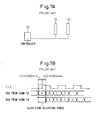
- FIGs 7A and 7B are diagrams for explaining how memory data are received by a controller. It is assumed that the controller 70 receives data by simultaneously accessing the DIMM 72 inserted in the first slot and the DIMM 74 inserted in the second slot, as shown in Figure 7A.
- the delay times from when the CLK is input to the DIMMs until the output data are produced from them are designated by tCLKDQSmin (a negative value) and tCLKDQSmax (a positive value), respectively.
- the present invention provides a memory module designed so that the phase of the clock to be distributed via the PLL circuit can be adjusted by an external signal, thereby making it possible to receive memory read data at the same time.
- FIG 8 is a diagram showing the circuit configuration of a DIMM according to one embodiment of the present invention. As shown, the circuit differs from the circuit previously shown in Figure 2 by the inclusion of a capacitance switching circuit 80 and a register 86. Here, the register 86 may be provided on the controller side. As shown in the figure, the capacitance switching circuit 80 is constructed by paralleling a plurality of series connections each consisting of a transistor 82 and a capacitor 84, and the circuit as a whole is connected in parallel with the resistor 24 and capacitor 26 in the feedback loop.
- each bit in the register 86 controls the on/off operation of the corresponding transistor 82; that is, when the bit value is "0", the transistor 82 is cut off, and when the bit value is "1", the transistor 82 conducts. Accordingly, the controller for controlling the DIMM can vary the capacitance in the feedback loop by varying the value of the register and thereby controlling the number of capacitors 84 to be inserted in the feedback loop of the PLL.
- the controller can make a phase adjustment in accordance with such changes.
- the capacitance switching circuit 80 may be replaced by a resistance switching circuit having a similar circuit configuration.
- a circuit for varying both the capacitance and resistance may be provided.
- FIG 9 is a diagram for explaining a DIMM according to another embodiment of the present invention.
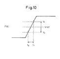
- the controller supplies a signal Vref to the PLL-based clock driver 20.
- the signal Vref is a signal for varying the threshold of the buffer 32 in the PLL-based clock driver 20 shown in Figure 3.
- SIMMs Single In-line Memory Modules
Landscapes
- Engineering & Computer Science (AREA)
- Microelectronics & Electronic Packaging (AREA)
- Computer Hardware Design (AREA)
- Dram (AREA)
- Static Random-Access Memory (AREA)
- Stabilization Of Oscillater, Synchronisation, Frequency Synthesizers (AREA)
- Memory System (AREA)
Applications Claiming Priority (1)
| Application Number | Priority Date | Filing Date | Title |
|---|---|---|---|
| JP2006050770A JP2007233453A (ja) | 2006-02-27 | 2006-02-27 | メモリモジュール |
Publications (2)
| Publication Number | Publication Date |
|---|---|
| EP1826769A2 true EP1826769A2 (de) | 2007-08-29 |
| EP1826769A3 EP1826769A3 (de) | 2008-05-07 |
Family
ID=38134830
Family Applications (1)
| Application Number | Title | Priority Date | Filing Date |
|---|---|---|---|
| EP07250166A Withdrawn EP1826769A3 (de) | 2006-02-27 | 2007-01-17 | Speichermodul |
Country Status (6)
| Country | Link |
|---|---|
| US (1) | US20070201282A1 (de) |
| EP (1) | EP1826769A3 (de) |
| JP (1) | JP2007233453A (de) |
| KR (1) | KR20070089050A (de) |
| CN (1) | CN101030442A (de) |
| TW (1) | TW200732882A (de) |
Families Citing this family (3)
| Publication number | Priority date | Publication date | Assignee | Title |
|---|---|---|---|---|
| US7391656B2 (en) * | 2006-07-25 | 2008-06-24 | Etron Technology, Inc. | Self-feedback control pipeline architecture for memory read path applications |
| US8375241B2 (en) * | 2009-04-02 | 2013-02-12 | Intel Corporation | Method and system to improve the operations of a registered memory module |
| KR102701857B1 (ko) * | 2016-09-13 | 2024-09-03 | 삼성전자주식회사 | 차동 신호를 수신하는 반도체 장치, 메모리 컨트롤러 및 그 동작 방법 |
Family Cites Families (5)
| Publication number | Priority date | Publication date | Assignee | Title |
|---|---|---|---|---|
| US6028488A (en) * | 1996-11-08 | 2000-02-22 | Texas Instruments Incorporated | Digitally-controlled oscillator with switched-capacitor frequency selection |
| JP3037215B2 (ja) * | 1997-06-24 | 2000-04-24 | 日本電気アイシーマイコンシステム株式会社 | 半導体集積回路 |
| US6868504B1 (en) * | 2000-08-31 | 2005-03-15 | Micron Technology, Inc. | Interleaved delay line for phase locked and delay locked loops |
| KR100378194B1 (ko) * | 2001-02-19 | 2003-03-29 | 삼성전자주식회사 | 반도체 메모리 장치의 입력 신호의 셋업 시간 및 홀드시간을 조정할 수 있는 메모리 모듈 및 방법 |
| US6784752B2 (en) * | 2002-04-24 | 2004-08-31 | Sun Microsystems, Inc. | Post-silicon phase offset control of phase locked loop input receiver |
-
2006
- 2006-02-27 JP JP2006050770A patent/JP2007233453A/ja not_active Withdrawn
- 2006-08-31 US US11/513,225 patent/US20070201282A1/en not_active Abandoned
-
2007
- 2007-01-16 TW TW096101594A patent/TW200732882A/zh unknown
- 2007-01-17 EP EP07250166A patent/EP1826769A3/de not_active Withdrawn
- 2007-01-31 KR KR1020070009856A patent/KR20070089050A/ko not_active Ceased
- 2007-02-06 CN CNA2007100035585A patent/CN101030442A/zh active Pending
Also Published As
| Publication number | Publication date |
|---|---|
| TW200732882A (en) | 2007-09-01 |
| EP1826769A3 (de) | 2008-05-07 |
| CN101030442A (zh) | 2007-09-05 |
| US20070201282A1 (en) | 2007-08-30 |
| JP2007233453A (ja) | 2007-09-13 |
| KR20070089050A (ko) | 2007-08-30 |
Similar Documents
| Publication | Publication Date | Title |
|---|---|---|
| US7593273B2 (en) | Read-leveling implementations for DDR3 applications on an FPGA | |
| US6282210B1 (en) | Clock driver with instantaneously selectable phase and method for use in data communication systems | |
| EP2197143B1 (de) | Vorrichtung zur Datenwiederherstellung in einem synchronen Chip-zu-Chip System | |
| US5935257A (en) | Skew-reduction circuit and semiconductor device | |
| US9306584B2 (en) | Multi-function delay locked loop | |
| US7827431B2 (en) | Memory card having memory device and host apparatus accessing memory card | |
| US20030215040A1 (en) | Delay locked loop with frequency control | |
| US7298188B2 (en) | Timing adjustment circuit and memory controller | |
| US6510473B1 (en) | Apparatus and method for automatically selecting an appropriate signal from a plurality of signals, based on the configuration of a peripheral installed within a computing device | |
| WO2002023358A2 (en) | Digital system of adjusting delays on circuit boards | |
| KR100483641B1 (ko) | 반도체 집적 회로 및 메모리 시스템 | |
| EP1826769A2 (de) | Speichermodul | |
| US20250175318A1 (en) | Power Efficient Circuits and Methods for Phase Alignment | |
| US20030226055A1 (en) | Controller of electronic equipment and clock skew adjusting method | |
| US7197659B2 (en) | Global I/O timing adjustment using calibrated delay elements | |
| KR19990006533A (ko) | 위상조정기능을 갖는 반도체 집적회로 및 이를 사용하는 시스템 | |
| KR100588593B1 (ko) | 레지스터형 메모리 모듈 및 그 제어방법 | |
| JP2006344216A (ja) | レジスタ型メモリモジュール及びこれを含むメモリシステム並びにその制御方法 | |
| KR100847759B1 (ko) | 레지스터 칩 | |
| JPH09190239A (ja) | クロックスキュー調整回路 |
Legal Events
| Date | Code | Title | Description |
|---|---|---|---|
| PUAI | Public reference made under article 153(3) epc to a published international application that has entered the european phase |
Free format text: ORIGINAL CODE: 0009012 |
|
| AK | Designated contracting states |
Kind code of ref document: A2 Designated state(s): AT BE BG CH CY CZ DE DK EE ES FI FR GB GR HU IE IS IT LI LT LU LV MC NL PL PT RO SE SI SK TR |
|
| AX | Request for extension of the european patent |
Extension state: AL BA HR MK YU |
|
| PUAL | Search report despatched |
Free format text: ORIGINAL CODE: 0009013 |
|
| AK | Designated contracting states |
Kind code of ref document: A3 Designated state(s): AT BE BG CH CY CZ DE DK EE ES FI FR GB GR HU IE IS IT LI LT LU LV MC NL PL PT RO SE SI SK TR |
|
| AX | Request for extension of the european patent |
Extension state: AL BA HR MK RS |
|
| STAA | Information on the status of an ep patent application or granted ep patent |
Free format text: STATUS: THE APPLICATION HAS BEEN WITHDRAWN |
|
| 18W | Application withdrawn |
Effective date: 20080930 |