EP1815990A1 - Inkjet printhead having piezoelectric actuator and method of driving the piezoelectric actuator - Google Patents
Inkjet printhead having piezoelectric actuator and method of driving the piezoelectric actuator Download PDFInfo
- Publication number
- EP1815990A1 EP1815990A1 EP06251952A EP06251952A EP1815990A1 EP 1815990 A1 EP1815990 A1 EP 1815990A1 EP 06251952 A EP06251952 A EP 06251952A EP 06251952 A EP06251952 A EP 06251952A EP 1815990 A1 EP1815990 A1 EP 1815990A1
- Authority
- EP
- European Patent Office
- Prior art keywords
- piezoelectric
- piezoelectric layer
- driving
- piezoelectric actuator
- inkjet printhead
- Prior art date
- Legal status (The legal status is an assumption and is not a legal conclusion. Google has not performed a legal analysis and makes no representation as to the accuracy of the status listed.)
- Withdrawn
Links
Images

Classifications
-
- B—PERFORMING OPERATIONS; TRANSPORTING
- B41—PRINTING; LINING MACHINES; TYPEWRITERS; STAMPS
- B41J—TYPEWRITERS; SELECTIVE PRINTING MECHANISMS, i.e. MECHANISMS PRINTING OTHERWISE THAN FROM A FORME; CORRECTION OF TYPOGRAPHICAL ERRORS
- B41J2/00—Typewriters or selective printing mechanisms characterised by the printing or marking process for which they are designed
- B41J2/005—Typewriters or selective printing mechanisms characterised by the printing or marking process for which they are designed characterised by bringing liquid or particles selectively into contact with a printing material
- B41J2/01—Ink jet
- B41J2/135—Nozzles
- B41J2/14—Structure thereof only for on-demand ink jet heads
- B41J2/14201—Structure of print heads with piezoelectric elements
- B41J2/14233—Structure of print heads with piezoelectric elements of film type, deformed by bending and disposed on a diaphragm
-
- A—HUMAN NECESSITIES
- A61—MEDICAL OR VETERINARY SCIENCE; HYGIENE
- A61C—DENTISTRY; APPARATUS OR METHODS FOR ORAL OR DENTAL HYGIENE
- A61C1/00—Dental machines for boring or cutting ; General features of dental machines or apparatus, e.g. hand-piece design
- A61C1/08—Machine parts specially adapted for dentistry
- A61C1/14—Tool-holders, i.e. operating tool holders, e.g. burr holders
- A61C1/142—Operating tool blocking means
- A61C1/144—Operating tool blocking means constricting the operating tool, e.g. chuck
-
- A—HUMAN NECESSITIES
- A61—MEDICAL OR VETERINARY SCIENCE; HYGIENE
- A61C—DENTISTRY; APPARATUS OR METHODS FOR ORAL OR DENTAL HYGIENE
- A61C1/00—Dental machines for boring or cutting ; General features of dental machines or apparatus, e.g. hand-piece design
- A61C1/08—Machine parts specially adapted for dentistry
- A61C1/14—Tool-holders, i.e. operating tool holders, e.g. burr holders
- A61C1/145—Instruments or accessories for tool holders
-
- A—HUMAN NECESSITIES
- A61—MEDICAL OR VETERINARY SCIENCE; HYGIENE
- A61C—DENTISTRY; APPARATUS OR METHODS FOR ORAL OR DENTAL HYGIENE
- A61C1/00—Dental machines for boring or cutting ; General features of dental machines or apparatus, e.g. hand-piece design
- A61C1/08—Machine parts specially adapted for dentistry
- A61C1/18—Flexible shafts; Clutches or the like; Bearings or lubricating arrangements; Drives or transmissions
- A61C1/185—Drives or transmissions
Definitions
- the present invention relates to an inkjet printhead that ejects ink using a piezoelectric actuator, and a method of driving the piezoelectric actuator.
- inkjet printheads are devices for printing an image on a printing medium by firing droplets of ink onto a desired region of the printing medium.
- the inkjet printheads can be classified into two types.
- One is a thermal inkjet printhead, in which ink is heated to form ink bubbles and the expansive force of the bubbles causes ink droplets to be ejected.
- the other is a piezoelectric inkjet printhead, in which a piezoelectric crystal is deformed and the pressure due to the deformation of the piezoelectric crystal causes ink droplets to be ejected.
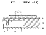
- FIG. 1 is a vertical section showing a general structure of a conventional piezoelectric inkjet printhead.
- a manifold 13, a plurality of restrictors 12, and a plurality of pressure chambers 11 are included in a flow channel substrate 10 to form an ink flow channel.
- a plurality of nozzles 22 corresponding to the pressure chambers 11 is formed in a nozzle substrate 20.
- a piezoelectric actuator 40 is formed on the flow channel substrate 10.
- the manifold 13 is a passage allowing inflow of ink from an ink reservoir (not shown) to the pressure chambers 11, and the restrictors 12 is a passage allowing inflow of the ink from the manifold 13 to the pressure chambers 11.
- the pressure chambers 11 are arranged along one side or both sides of the manifold 13 to store ink to be ejected through the nozzles 22.
- the volume of the pressure chamber 11 varies according to the operation of the piezoelectric actuator 40.
- ink flows into or out of the pressure chamber 11 according to the pressure variation.
- a portion of the flow channel substrate 10 forming an upper wall of the press chamber 11 is used as a vibrating plate 14.
- the vibrating plate 14 is deformed by the operation of the piezoelectric actuator 40.
- the piezoelectric actuator 40 includes a lower electrode 41, a piezoelectric layer 42, and an upper electrode 43 that are sequentially stacked on the flow channel substrate 10.
- a silicon oxide layer 31 is formed between the lower electrode 41 and the flow channel substrate 10 as an insulating layer.
- the lower electrode 41 is formed on the entire surface of the silicon oxide layer 31 as a common electrode.
- the piezoelectric layer 42 is formed on the lower electrode 41 above the pressure chamber 11.
- the upper electrode 43 is formed on the piezoelectric layer 42 as a driving electrode for applying a voltage to the piezoelectric layer 42.
- a flexible printed circuit (FPC) 50 is connected to the upper electrode 43 for applying a voltage to the upper electrode 43.
- the piezoelectric layer 42 When a driving pulse is applied to the upper electrode 43, the piezoelectric layer 42 is deformed, thereby bending the vibrating plate 14 and thus changing the volume of the pressure chamber 11. By this, ink contained in the pressure chamber 11 is ejected through the nozzle 22.
- the deformation of the vibrating plate 14 should be large to effectively eject ink having various viscosities.
- the deformation of the vibrating plate 14 depends on the deformation amount of the piezoelectric layer 42 in a transverse direction.
- the transverse deformation of the piezoelectric layer 42 depends on the transverse length of the piezoelectric layer 42 and the magnitude of the driving voltage applied to the piezoelectric layer 42. However, the transverse length of the piezoelectric layer 42 is restricted by the length of the pressure chamber 11.
- the driving voltage to the piezoelectric layer 42 should be large to increase the deformation of the vibrating plate 14.
- the transverse deformation of the piezoelectric layer 42 depends on the thickness uniformity of the piezoelectric layer 42. That is, if the thickness of the piezoelectric layer 42 is not uniform, the transverse deformation of the piezoelectric layer 42 is affected by the thickness variation.
- an inkjet printhead including: a flow channel substrate having a pressure chamber; and a piezoelectric actuator formed on the flow channel substrate to apply a driving force to the pressure chamber for ejecting ink, the piezoelectric actuator having a piezoelectric layer formed on the flow channel substrate in correspondence with the pressure chamber, and a plurality of common electrodes and a plurality of driving electrodes alternately arranged in a length direction of the piezoelectric layer.
- An insulating layer may be formed between the flow channel substrate and the piezoelectric actuator.
- the common electrodes and the driving electrodes may be formed on the piezoelectric layer.
- a method of driving a piezoelectric actuator of an inkjet printhead including a flow channel substrate having a pressure chamber, wherein the piezoelectric actuator is formed on the flow channel substrate to apply a driving force to the pressure chamber for ejecting ink, the method including: dividing a piezoelectric layer of the piezoelectric actuator into a plurality of sections in a length direction of the piezoelectric layer; and applying a driving electric field to each of the sections in the length direction.
- the present invention thus provides a piezoelectric inkjet printhead that operates using a low driving voltage and is less affected by the thickness uniformity of a piezoelectric layer, and a method of driving the piezoelectric inkjet printhead.
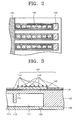
- FIG. 2 is a plan view of a piezoelectric inkjet printhead according to an embodiment of the present invention
- FIG. 3 is a vertical section showing a structure of the piezoelectric inkjet printhead depicted in FIG. 2 along a length direction of a piezoelectric layer.
- the piezoelectric inkjet printhead includes a flow channel substrate 110 in which an ink flow channel is formed, and a piezoelectric actuator 140 providing an ink ejecting pressure.
- the flow channel substrate 110 includes a pressure chamber 111, a manifold 113 supplying ink to the pressure chamber 111, and a restrictor 112.
- a nozzle substrate 120 is bonded to a bottom surface of the flow channel substrate 110 and includes a nozzle 122 ejecting the ink contained in the pressure chamber 111.
- a vibrating plate 114 is formed on a top area of the pressure chamber 111 and is deformed by the operation of the piezoelectric actuator 140.
- An ink flow channel is defined by the flow channel substrate 110 and the nozzle substrate 120.
- the piezoelectric actuator 140 is formed on the flow channel substrate 110 to apply a driving force to the pressure chamber 111 for ejecting ink.
- the piezoelectric actuator 140 includes common electrodes 141, a piezoelectric layer 142 deformable in response to an applied voltage, and driving electrodes 143 receiving a driving voltage.
- the common electrodes 141, the piezoelectric layer 142, and the driving electrodes 143 are stacked on the flow channel substrate 110.
- an insulating layer 131 may be formed between the piezoelectric actuator 140 and the flow channel substrate 110.
- the insulating layer 131 may be a silicon oxide layer formed on the flow channel substrate 110 by plasma enhanced chemical vapor deposition (PECVD).
- the piezoelectric layer 142 is formed by screen-printing a piezoelectric material paste onto the insulating layer 131 to a predetermined thickness.
- the piezoelectric layer 142 is formed on a region corresponding to the pressure chamber 111.
- PZT lead zirconate titanate
- the piezoelectric layer 142 is divided into a plurality of sections in a length direction thereof, and a driving electric field is applied to each sections, respectively.
- the common electrodes 141 and the driving electrodes 143 are alternately arranged along the length direction of the piezoelectric layer 142.
- the common electrodes 141 and the driving electrodes 143 are formed of conductive metals.
- the common electrodes 141 and the driving electrodes 143 may be formed by one metal layer or two metal layers such as a titanium (Ti) layer and a platinum (Pt) layer.
- the common electrodes 141 and the driving electrodes 143 may be formed by respectively depositing Ti and Pt onto the insulating layer 131 and the piezoelectric layer 142 using a sputtering process.
- the common electrodes 141 and the driving electrodes 143 may be formed by screen-printing a conductive metal such as Ag-Pd paste onto the piezoelectric layer 142.
- the piezoelectric layer 142, the common electrodes 141, and the driving electrodes 143 are sintered at a predetermined temperature, for example, 900 to 1,000 °C. After that, a polling process is performed on the piezoelectric layer 142 by applying an electric field to the piezoelectric layer 142 to activate the piezoelectric characteristic of the piezoelectric layer 142.
- the common electrodes 141 and the driving electrodes 143 may be formed between the piezoelectric layer 142 and the insulating layer 131.
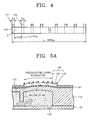
- one hundred common electrodes 141 and one hundred driving electrodes 143 are arranged in the length direction of the piezoelectric layer 142.
- the piezoelectric layer 142 is divided into one hundred and ninety nine sections (S).
- the length of the piezoelectric inkjet printhead layer 142 is 3000 ⁇ m, and the widths of the common electrodes 141 and the driving electrodes 143 are respectively 5 ⁇ m, the length of each section (S) is approximately 10.05 ⁇ m (hereinafter, assumed to be 10 ⁇ m).
- a total effective length of the piezoelectric layer 142 is 1990 ⁇ m (199 x 10 ⁇ m).
- the length variation rate (Lr) is 1300 ⁇ m/m.
- the length variation rate (Lr) of 1300 ⁇ m/m by 1990 ⁇ m (the total effective length of the piezoelectric layer 142)
- the total length variation value of the piezoelectric layer 142 is 2587 nm.
- the length variation value of the piezoelectric layer 42 of the conventional piezoelectric actuator 40 shown in FIG. 1 will now be calculated.
- the piezoelectric layer 42 is polarized in its thickness direction, and elongated in the thickness direction when a driving voltage is applied to the upper electrode 43. Therefore, the piezoelectric layer 42 shrinks in a direction perpendicular to its thickness direction.
- the thickness (T) of the piezoelectric layer 42 is 25 ⁇ m
- the length (L) of the piezoelectric layer 42 is 3000 ⁇ m
- a voltage of 65 V is applied to the upper electrode 43
- the deformation amount of the piezoelectric actuator 140 of the present invention is approximately 3.3 times higher than that of the conventional piezoelectric actuator 40.
- the deformation amount of the piezoelectric actuator 140 can be largely increased compared with the conventional piezoelectric actuator 40 by dividing the piezoelectric layer 142 into the plurality of sections (S) and applying a driving voltage to the respective sections (S). This fact can be easily checked by simple calculations.
- the length variation value of the piezoelectric layer 142 increases as the number of sections (S) increases (i.e., as the widths of the common electrodes 141 and the driving electrodes 143, and the length L 3 of the respective sections (S) become smaller). Therefore, according to the present invention, the piezoelectric actuator 140 of the piezoelectric inkjet printhead can be deformed much more than the conventional piezoelectric actuator when the size of the piezoelectric layer 142 and the driving voltage V 3 are the same as those of the conventional piezoelectric actuator.
- the piezoelectric coefficient d 31 is a transverse piezoelectric coefficient defined in a direction perpendicular to the polarization direction (the thickness direction of the piezoelectric layer 42). Therefore, the piezoelectric actuator 40 can be stably driven only when the thickness of the piezoelectric layer 42 is uniform.
- the piezoelectric coefficient d 33 is a longitudinal piezoelectric coefficient defined in the same direction as the polarization direction (the length direction of the piezoelectric layer 142).
- the deformation amount of the piezoelectric layer 142 is not largely affected by the thickness uniformity of the piezoelectric layer 142. That is, the piezoelectric actuator 140 can be uniformly deformed if the common electrodes 141 and the driving electrodes 143 are uniformly formed. As a result, the inkjet printhead of the present invention can print images with uniform quality.
- the piezoelectric actuator 140 can be deformed to a desired degree with a much lower driving voltage by dividing the piezoelectric layer 142 into a plurality of sections, a low-voltage piezoelectric inkjet printhead can be provided.
- the silicon oxide layer 31 is formed on the flow channel substrate 10, and the lower electrode 41 is formed on the silicon oxide layer 31.
- the piezoelectric layer 42 is formed on the lower electrode 41.
- the upper electrode 43 is formed on the piezoelectric layer 42.
- a silicon oxide layer is formed on the flow channel substrate 110 as the insulating layer 131, and the piezoelectric layer 142 is formed on the insulating layer 131.
- the common electrodes 141 and the driving electrodes 143 are simultaneously formed on the piezoelectric layer 142 and the insulating layer 131. Therefore, the electrodes 141 and 143 can be formed through a simple process with less cost when compared with the conventional inkjet printhead.
- the piezoelectric layer 142 is elongated, thereby bending the vibrating plate 114 upward and therefore increasing the volume of the pressure chamber 111.
- ink flows from an ink reservoir (not shown) into the pressure chamber 111 through the manifold 113 and the restrictor 112.
- the piezoelectric layer 142 and the vibrating plate 114 return to their original shapes, and thus the volume of the pressure chamber 111 is reduced.
- the ink contained in the pressure chamber 111 is ejected through the nozzle 122.
- Ink can be successively ejected through the nozzle 122 by applying a driving pulse voltage to the driving electrodes 143.
- the piezoelectric inkjet printhead and the method of driving the piezoelectric inkjet printhead are characterized in that the piezoelectric layer 142 of the piezoelectric actuator 140 is divided into a plurality of sections (S) along the length of the piezoelectric layer 142 and a driving electric field is applied to each of the sections (S) using the electrodes 141 and 143.
- the flow channel substrate 110 and the nozzle substrate 120 shown in FIGS. 2 and 3 are exemplary. That is, various other ink flow channels can be formed in the piezoelectric inkjet printhead of the present invention. Further, the ink flow channel can be formed using a number of substrates instead of using two substrates 110 and 120 shown in FIG. 3.
- the piezoelectric inkjet printhead and the method of driving the piezoelectric inkjet printhead have the following advantages.
- the piezoelectric layer is divided into a plurality of sections and a driving electric field is applied to each of the sections, the deformation amount of the piezoelectric layer of the piezoelectric actuator can be largely increased using the same piezoelectric layer and driving voltage when compared with the conventional piezoelectric actuator.
- the same deformation amount of the piezoelectric actuator can be obtained using a much lower driving voltage by dividing the piezoelectric layer into a plurality of sections. Therefore, a low-voltage piezoelectric inkjet printhead can be provided.
- the deformation amount of the piezoelectric layer is calculated using the longitudinal piezoelectric coefficient d 33 in the piezoelectric actuator of the inkjet printhead of the present invention, the deformation amount of deformation of the piezoelectric layer is less affected by the thickness of the piezoelectric layer.
- the common electrodes and the driving electrodes can be simultaneously formed on the piezoelectric layer, so that the process of forming the electrodes can be simplified, and thus manufacturing cost can be reduced.
Landscapes
- Health & Medical Sciences (AREA)
- Oral & Maxillofacial Surgery (AREA)
- Dentistry (AREA)
- Epidemiology (AREA)
- Life Sciences & Earth Sciences (AREA)
- Animal Behavior & Ethology (AREA)
- General Health & Medical Sciences (AREA)
- Public Health (AREA)
- Veterinary Medicine (AREA)
- Particle Formation And Scattering Control In Inkjet Printers (AREA)
Abstract
Description
- The present invention relates to an inkjet printhead that ejects ink using a piezoelectric actuator, and a method of driving the piezoelectric actuator.
- Generally, inkjet printheads are devices for printing an image on a printing medium by firing droplets of ink onto a desired region of the printing medium. Depending on the ink ejecting method, the inkjet printheads can be classified into two types. One is a thermal inkjet printhead, in which ink is heated to form ink bubbles and the expansive force of the bubbles causes ink droplets to be ejected. The other is a piezoelectric inkjet printhead, in which a piezoelectric crystal is deformed and the pressure due to the deformation of the piezoelectric crystal causes ink droplets to be ejected.
- FIG. 1 is a vertical section showing a general structure of a conventional piezoelectric inkjet printhead. Referring to FIG. 1, a
manifold 13, a plurality ofrestrictors 12, and a plurality ofpressure chambers 11 are included in aflow channel substrate 10 to form an ink flow channel. A plurality ofnozzles 22 corresponding to thepressure chambers 11 is formed in anozzle substrate 20. Apiezoelectric actuator 40 is formed on theflow channel substrate 10. Themanifold 13 is a passage allowing inflow of ink from an ink reservoir (not shown) to thepressure chambers 11, and therestrictors 12 is a passage allowing inflow of the ink from themanifold 13 to thepressure chambers 11. Thepressure chambers 11 are arranged along one side or both sides of themanifold 13 to store ink to be ejected through thenozzles 22. The volume of thepressure chamber 11 varies according to the operation of thepiezoelectric actuator 40. Thus, ink flows into or out of thepressure chamber 11 according to the pressure variation. For this, a portion of theflow channel substrate 10 forming an upper wall of thepress chamber 11 is used as avibrating plate 14. The vibratingplate 14 is deformed by the operation of thepiezoelectric actuator 40. - The
piezoelectric actuator 40 includes alower electrode 41, apiezoelectric layer 42, and anupper electrode 43 that are sequentially stacked on theflow channel substrate 10. Asilicon oxide layer 31 is formed between thelower electrode 41 and theflow channel substrate 10 as an insulating layer. Thelower electrode 41 is formed on the entire surface of thesilicon oxide layer 31 as a common electrode. Thepiezoelectric layer 42 is formed on thelower electrode 41 above thepressure chamber 11. Theupper electrode 43 is formed on thepiezoelectric layer 42 as a driving electrode for applying a voltage to thepiezoelectric layer 42. A flexible printed circuit (FPC) 50 is connected to theupper electrode 43 for applying a voltage to theupper electrode 43. - When a driving pulse is applied to the
upper electrode 43, thepiezoelectric layer 42 is deformed, thereby bending the vibratingplate 14 and thus changing the volume of thepressure chamber 11. By this, ink contained in thepressure chamber 11 is ejected through thenozzle 22. The deformation of the vibratingplate 14 should be large to effectively eject ink having various viscosities. The deformation of thevibrating plate 14 depends on the deformation amount of thepiezoelectric layer 42 in a transverse direction. The transverse deformation of thepiezoelectric layer 42 depends on the transverse length of thepiezoelectric layer 42 and the magnitude of the driving voltage applied to thepiezoelectric layer 42. However, the transverse length of thepiezoelectric layer 42 is restricted by the length of thepressure chamber 11. Therefore, in thepiezoelectric actuator 40 shown in FIG. 1, the driving voltage to thepiezoelectric layer 42 should be large to increase the deformation of thevibrating plate 14. Further, the transverse deformation of thepiezoelectric layer 42 depends on the thickness uniformity of thepiezoelectric layer 42. That is, if the thickness of thepiezoelectric layer 42 is not uniform, the transverse deformation of thepiezoelectric layer 42 is affected by the thickness variation. - According to an aspect of the present invention, there is provided an inkjet printhead including: a flow channel substrate having a pressure chamber; and a piezoelectric actuator formed on the flow channel substrate to apply a driving force to the pressure chamber for ejecting ink, the piezoelectric actuator having a piezoelectric layer formed on the flow channel substrate in correspondence with the pressure chamber, and a plurality of common electrodes and a plurality of driving electrodes alternately arranged in a length direction of the piezoelectric layer.
- An insulating layer may be formed between the flow channel substrate and the piezoelectric actuator.
- The common electrodes and the driving electrodes may be formed on the piezoelectric layer.
- According to another aspect of the present invention, there is provided a method of driving a piezoelectric actuator of an inkjet printhead including a flow channel substrate having a pressure chamber, wherein the piezoelectric actuator is formed on the flow channel substrate to apply a driving force to the pressure chamber for ejecting ink, the method including: dividing a piezoelectric layer of the piezoelectric actuator into a plurality of sections in a length direction of the piezoelectric layer; and applying a driving electric field to each of the sections in the length direction.
- The present invention thus provides a piezoelectric inkjet printhead that operates using a low driving voltage and is less affected by the thickness uniformity of a piezoelectric layer, and a method of driving the piezoelectric inkjet printhead.
- The above and other features and advantages of the present invention will become more apparent by describing in detail exemplary embodiments thereof with reference to the attached drawings in which:
- FIG. 1 is a vertical section showing a general structure of a conventional piezoelectric inkjet printhead;
- FIG. 2 is a plan view showing a structure of an inkjet printhead according to an embodiment of the present invention;
- FIG. 3 is a vertical section of the inkjet printhead depicted in FIG. 2;
- FIG. 4 is a vertical section showing an operation of the inkjet printhead depicted in FIG. 2; and
- FIGS. 5A and 5B show an ink ejecting operation of the inkjet printhead depicted in FIG. 2.
- In the drawings, like reference numerals denote like elements, and the thicknesses of layers and regions are exaggerated for clarity. It will also be understood that when a layer is referred to as being "on" another layer or substrate, it can be directly on the other layer or substrate, or intervening layers may also be present. The present invention will now be described more fully with reference to the accompanying drawings, in which exemplary embodiments of the invention are shown.
- FIG. 2 is a plan view of a piezoelectric inkjet printhead according to an embodiment of the present invention, and FIG. 3 is a vertical section showing a structure of the piezoelectric inkjet printhead depicted in FIG. 2 along a length direction of a piezoelectric layer.
- Referring to FIGS. 2 and 3, the piezoelectric inkjet printhead includes a
flow channel substrate 110 in which an ink flow channel is formed, and apiezoelectric actuator 140 providing an ink ejecting pressure. Theflow channel substrate 110 includes apressure chamber 111, amanifold 113 supplying ink to thepressure chamber 111, and arestrictor 112. Anozzle substrate 120 is bonded to a bottom surface of theflow channel substrate 110 and includes anozzle 122 ejecting the ink contained in thepressure chamber 111. Avibrating plate 114 is formed on a top area of thepressure chamber 111 and is deformed by the operation of thepiezoelectric actuator 140. An ink flow channel is defined by theflow channel substrate 110 and thenozzle substrate 120. - The
piezoelectric actuator 140 is formed on theflow channel substrate 110 to apply a driving force to thepressure chamber 111 for ejecting ink. Thepiezoelectric actuator 140 includescommon electrodes 141, apiezoelectric layer 142 deformable in response to an applied voltage, and drivingelectrodes 143 receiving a driving voltage. Thecommon electrodes 141, thepiezoelectric layer 142, and thedriving electrodes 143 are stacked on theflow channel substrate 110. - If the
flow channel substrate 110 is formed of a silicon wafer, aninsulating layer 131 may be formed between thepiezoelectric actuator 140 and theflow channel substrate 110. For example, theinsulating layer 131 may be a silicon oxide layer formed on theflow channel substrate 110 by plasma enhanced chemical vapor deposition (PECVD). - The
piezoelectric layer 142 is formed by screen-printing a piezoelectric material paste onto theinsulating layer 131 to a predetermined thickness. Thepiezoelectric layer 142 is formed on a region corresponding to thepressure chamber 111. Although various piezoelectric materials can be used for thepiezoelectric layer 142, PZT (lead zirconate titanate) ceramic may be used for thepiezoelectric layer 142. - In the piezoelectric inkjet printhead of the present invention, the
piezoelectric layer 142 is divided into a plurality of sections in a length direction thereof, and a driving electric field is applied to each sections, respectively. For this, referring to FIG. 2, thecommon electrodes 141 and the drivingelectrodes 143 are alternately arranged along the length direction of thepiezoelectric layer 142. - The
common electrodes 141 and thedriving electrodes 143 are formed of conductive metals. Thecommon electrodes 141 and thedriving electrodes 143 may be formed by one metal layer or two metal layers such as a titanium (Ti) layer and a platinum (Pt) layer. Thecommon electrodes 141 and thedriving electrodes 143 may be formed by respectively depositing Ti and Pt onto theinsulating layer 131 and thepiezoelectric layer 142 using a sputtering process. Alternatively, thecommon electrodes 141 and the drivingelectrodes 143 may be formed by screen-printing a conductive metal such as Ag-Pd paste onto thepiezoelectric layer 142. In this case, thepiezoelectric layer 142, thecommon electrodes 141, and the drivingelectrodes 143 are sintered at a predetermined temperature, for example, 900 to 1,000 °C. After that, a polling process is performed on thepiezoelectric layer 142 by applying an electric field to thepiezoelectric layer 142 to activate the piezoelectric characteristic of thepiezoelectric layer 142. Thecommon electrodes 141 and the drivingelectrodes 143 may be formed between thepiezoelectric layer 142 and the insulatinglayer 131. - An example of how to calculate the deformation amount of the
piezoelectric layer 142 when thepiezoelectric actuator 140 operates will now be described with reference to FIG. 4. Referring to FIG. 4, one hundredcommon electrodes 141 and one hundred drivingelectrodes 143 are arranged in the length direction of thepiezoelectric layer 142. In this case, thepiezoelectric layer 142 is divided into one hundred and ninety nine sections (S). When the length of the piezoelectricinkjet printhead layer 142 is 3000 µm, and the widths of thecommon electrodes 141 and the drivingelectrodes 143 are respectively 5 µm, the length of each section (S) is approximately 10.05 µm (hereinafter, assumed to be 10 µm). Therefore, a total effective length of thepiezoelectric layer 142 is 1990 µm (199 x 10 µm). When an electric field is formed at the respective sections (S) by a driving voltage applied to the drivingelectrodes 143, thepiezoelectric layer 142 is elongated in the same direction as the polarization direction of thepiezoelectric layer 142. A length variation rate (Lr) of thepiezoelectric layer 142 in the polarization direction can be expressed by the following equation:
where d33 denotes a longitudinal piezoelectric coefficient in a length direction (the same as the polarization direction), E3 denotes the strength of an electric field, V3 denotes a voltage applied to the drivingelectrodes 143, and L3 denotes the length of the section (S). - The longitudinal piezoelectric coefficient d33 is two times higher than a transversal piezoelectric coefficient d31 in a transverse direction (perpendicular to the polarization direction). Therefore, the length variation rate (Lr) of the
piezoelectric layer 142 in the polarization direction can be expressed by the following equation:
- For example, when d31 = -100 x 10-12 m/V (the negative sign (-) means a decrease in the length of the piezoelectric layer 142), V3 = 65 V, and L3 = 10 µm, the length variation rate (Lr) is 1300 µm/m. By multiplying the length variation rate (Lr) of 1300 µm/m by 1990 µm (the total effective length of the piezoelectric layer 142), a total length variation value of the
piezoelectric layer 142 is 2.587 µm = 2587 nm. Consequently, when thepiezoelectric layer 142 having a length of 3000 µm is divided into one hundred and ninety nine 10-µm sections (S) by thecommon electrodes 141 having a width of 5 µm and the drivingelectrodes 143 having a width of 5 µm, the total length variation value of thepiezoelectric layer 142 is 2587 nm. - The length variation value of the
piezoelectric layer 42 of the conventionalpiezoelectric actuator 40 shown in FIG. 1 will now be calculated. Thepiezoelectric layer 42 is polarized in its thickness direction, and elongated in the thickness direction when a driving voltage is applied to theupper electrode 43. Therefore, thepiezoelectric layer 42 shrinks in a direction perpendicular to its thickness direction. When the thickness (T) of thepiezoelectric layer 42 is 25 µm, the length (L) of thepiezoelectric layer 42 is 3000 µm, and a voltage of 65 V is applied to theupper electrode 43,
piezoelectric layer 42 decreases by 780 nm. - When the two results are compared, the deformation amount of the
piezoelectric actuator 140 of the present invention is approximately 3.3 times higher than that of the conventionalpiezoelectric actuator 40. Although other parameters such as the thickness and length of thepiezoelectric layer 142 and the magnitude of the driving voltage are not changed, the deformation amount of thepiezoelectric actuator 140 can be largely increased compared with the conventionalpiezoelectric actuator 40 by dividing thepiezoelectric layer 142 into the plurality of sections (S) and applying a driving voltage to the respective sections (S). This fact can be easily checked by simple calculations. - In FIG. 4, if the numbers of the
common electrodes 141 and the drivingelectrodes 143 are n/2, respectively, the total length of thepiezoelectric layer 142 is L, and the length of the respective sections (S) is L3, the total effective length of thepiezoelectric layer 142 is (n - 1) x L3. Therefore, the length variation value of thepiezoelectric layer 142 is as follows:
- That is, the length variation value of the
piezoelectric layer 142 increases as the number of sections (S) increases (i.e., as the widths of thecommon electrodes 141 and the drivingelectrodes 143, and the length L3 of the respective sections (S) become smaller). Therefore, according to the present invention, thepiezoelectric actuator 140 of the piezoelectric inkjet printhead can be deformed much more than the conventional piezoelectric actuator when the size of thepiezoelectric layer 142 and the driving voltage V3 are the same as those of the conventional piezoelectric actuator. In calculating the deformation amount of thepiezoelectric layer 42 of the conventionalpiezoelectric actuator 40, the piezoelectric coefficient d31 is a transverse piezoelectric coefficient defined in a direction perpendicular to the polarization direction (the thickness direction of the piezoelectric layer 42). Therefore, thepiezoelectric actuator 40 can be stably driven only when the thickness of thepiezoelectric layer 42 is uniform. However, according to the present invention, in calculating the deformation amount of thepiezoelectric layer 142 of thepiezoelectric actuator 140, the piezoelectric coefficient d33 is a longitudinal piezoelectric coefficient defined in the same direction as the polarization direction (the length direction of the piezoelectric layer 142). Therefore, the deformation amount of thepiezoelectric layer 142 is not largely affected by the thickness uniformity of thepiezoelectric layer 142. That is, thepiezoelectric actuator 140 can be uniformly deformed if thecommon electrodes 141 and the drivingelectrodes 143 are uniformly formed. As a result, the inkjet printhead of the present invention can print images with uniform quality. - Further, since the
piezoelectric actuator 140 can be deformed to a desired degree with a much lower driving voltage by dividing thepiezoelectric layer 142 into a plurality of sections, a low-voltage piezoelectric inkjet printhead can be provided. - Furthermore, in the conventional inkjet printhead having the lower and
upper electrodes piezoelectric layer 42, thesilicon oxide layer 31 is formed on theflow channel substrate 10, and thelower electrode 41 is formed on thesilicon oxide layer 31. Next, thepiezoelectric layer 42 is formed on thelower electrode 41. Then, theupper electrode 43 is formed on thepiezoelectric layer 42. However, in the inkjet printhead of the present invention, a silicon oxide layer is formed on theflow channel substrate 110 as the insulatinglayer 131, and thepiezoelectric layer 142 is formed on the insulatinglayer 131. Then, thecommon electrodes 141 and the drivingelectrodes 143 are simultaneously formed on thepiezoelectric layer 142 and the insulatinglayer 131. Therefore, theelectrodes - Referring to FIG. 5A, in the inkjet printhead of the present invention, when a driving voltage is applied to the driving
electrodes 143, thepiezoelectric layer 142 is elongated, thereby bending the vibratingplate 114 upward and therefore increasing the volume of thepressure chamber 111. By this, ink flows from an ink reservoir (not shown) into thepressure chamber 111 through the manifold 113 and therestrictor 112. Referring to FIG. 5B, when the driving voltage is removed from the drivingelectrodes 143, thepiezoelectric layer 142 and the vibratingplate 114 return to their original shapes, and thus the volume of thepressure chamber 111 is reduced. By a pressure wave caused by the reduction of the volume of thepressure chamber 111, the ink contained in thepressure chamber 111 is ejected through thenozzle 122. Ink can be successively ejected through thenozzle 122 by applying a driving pulse voltage to the drivingelectrodes 143. - According to the present invention, the piezoelectric inkjet printhead and the method of driving the piezoelectric inkjet printhead are characterized in that the
piezoelectric layer 142 of thepiezoelectric actuator 140 is divided into a plurality of sections (S) along the length of thepiezoelectric layer 142 and a driving electric field is applied to each of the sections (S) using theelectrodes flow channel substrate 110 and thenozzle substrate 120 shown in FIGS. 2 and 3 are exemplary. That is, various other ink flow channels can be formed in the piezoelectric inkjet printhead of the present invention. Further, the ink flow channel can be formed using a number of substrates instead of using twosubstrates - As described above, according to the present invention, the piezoelectric inkjet printhead and the method of driving the piezoelectric inkjet printhead have the following advantages.
- First, since the piezoelectric layer is divided into a plurality of sections and a driving electric field is applied to each of the sections, the deformation amount of the piezoelectric layer of the piezoelectric actuator can be largely increased using the same piezoelectric layer and driving voltage when compared with the conventional piezoelectric actuator.
- Secondly, the same deformation amount of the piezoelectric actuator can be obtained using a much lower driving voltage by dividing the piezoelectric layer into a plurality of sections. Therefore, a low-voltage piezoelectric inkjet printhead can be provided.
- Thirdly, since the deformation amount of the piezoelectric layer is calculated using the longitudinal piezoelectric coefficient d33 in the piezoelectric actuator of the inkjet printhead of the present invention, the deformation amount of deformation of the piezoelectric layer is less affected by the thickness of the piezoelectric layer.
- Fourthly, the common electrodes and the driving electrodes can be simultaneously formed on the piezoelectric layer, so that the process of forming the electrodes can be simplified, and thus manufacturing cost can be reduced.
- While the present invention has been particularly shown and described with reference to exemplary embodiments thereof, it will be understood by those of ordinary skill in the art that various changes in form and details may be made therein without departing from the scope of the present invention as defined by the following claims.
Claims (4)
- An inkjet printhead comprising:a flow channel substrate including a pressure chamber; anda piezoelectric actuator formed on the flow channel substrate and arranged to apply a driving force to the pressure chamber for ejecting ink, the piezoelectric actuator including a piezoelectric layer formed on the flow channel substrate in correspondence with the pressure chamber, and a plurality of common electrodes and a plurality of driving electrodes alternately arranged in a length direction of the piezoelectric layer.
- The inkjet printhead of claim 1, wherein an insulating layer is formed between the flow channel substrate and the piezoelectric actuator.
- The inkjet printhead of claim 1 or 2, wherein the common electrodes and the driving electrodes are formed on the piezoelectric layer.
- A method of driving a piezoelectric actuator of an inkjet printhead including a flow channel substrate having a pressure chamber, wherein the piezoelectric actuator is formed on the flow channel substrate and arranged to apply a driving force to the pressure chamber for ejecting ink, the method comprising:dividing a piezoelectric layer of the piezoelectric actuator into a plurality of sections in a length direction of the piezoelectric layer; andapplying a driving electric field to each of the sections in the length direction.
Applications Claiming Priority (1)
| Application Number | Priority Date | Filing Date | Title |
|---|---|---|---|
| KR1020060006583A KR100745758B1 (en) | 2006-01-21 | 2006-01-21 | Inkjet Printheads Employing Piezoelectric Actuators |
Publications (1)
| Publication Number | Publication Date |
|---|---|
| EP1815990A1 true EP1815990A1 (en) | 2007-08-08 |
Family
ID=38166136
Family Applications (1)
| Application Number | Title | Priority Date | Filing Date |
|---|---|---|---|
| EP06251952A Withdrawn EP1815990A1 (en) | 2006-01-21 | 2006-04-06 | Inkjet printhead having piezoelectric actuator and method of driving the piezoelectric actuator |
Country Status (4)
| Country | Link |
|---|---|
| US (2) | US7722166B2 (en) |
| EP (1) | EP1815990A1 (en) |
| JP (1) | JP2007190911A (en) |
| KR (1) | KR100745758B1 (en) |
Families Citing this family (2)
| Publication number | Priority date | Publication date | Assignee | Title |
|---|---|---|---|---|
| CN108705864B (en) * | 2018-07-26 | 2024-04-05 | 南京沃航智能科技有限公司 | High-efficiency low-voltage driving piezoelectric spray head |
| GB2602509A (en) * | 2021-01-05 | 2022-07-06 | Xaar Technology Ltd | Electrical element |
Citations (3)
| Publication number | Priority date | Publication date | Assignee | Title |
|---|---|---|---|---|
| US4520374A (en) * | 1981-10-07 | 1985-05-28 | Epson Corporation | Ink jet printing apparatus |
| US20040046838A1 (en) * | 2002-03-18 | 2004-03-11 | Seiko Epson Corporation | Piezoelectric element, piezoelectric actuator and liquid ejection head incorporating the same |
| US20050270340A1 (en) * | 2004-06-02 | 2005-12-08 | Fuji Photo Film Co., Ltd. | Laminated piezoelectric element, liquid droplet ejection head using same, and image forming apparatus comprising same |
Family Cites Families (18)
| Publication number | Priority date | Publication date | Assignee | Title |
|---|---|---|---|---|
| JPH06320723A (en) | 1993-05-12 | 1994-11-22 | Seiko Epson Corp | Ink jet head |
| US5983471A (en) * | 1993-10-14 | 1999-11-16 | Citizen Watch Co., Ltd. | Method of manufacturing an ink-jet head |
| US5589898A (en) | 1995-06-07 | 1996-12-31 | Reuters Limited | Method and system for color vision deficiency correction |
| JPH11157065A (en) | 1997-11-27 | 1999-06-15 | Fujitsu Ltd | Inkjet head |
| JP2002059544A (en) * | 2000-08-17 | 2002-02-26 | Seiko Epson Corp | Ink jet recording head, method of manufacturing the same, and ink jet recording apparatus |
| US6309117B1 (en) | 2000-08-17 | 2001-10-30 | Nortel Networks Limited | System and method for adjustment of color presentation in networked media |
| CN1157151C (en) | 2000-12-26 | 2004-07-14 | 陈言 | Color vision detecting and correcting method and equipment and its application |
| JP4362859B2 (en) * | 2001-01-26 | 2009-11-11 | セイコーエプソン株式会社 | Inkjet recording head and printer |
| US6931151B2 (en) | 2001-11-21 | 2005-08-16 | Intel Corporation | Method and apparatus for modifying graphics content prior to display for color blind use |
| US6623119B2 (en) | 2002-01-11 | 2003-09-23 | Hewlett-Packard Development Company, L.P. | System and method for modifying image-processing software in response to visual test results |
| JP2004066496A (en) * | 2002-08-01 | 2004-03-04 | Seiko Epson Corp | Liquid ejecting head and liquid ejecting apparatus |
| JP2004136461A (en) * | 2002-10-15 | 2004-05-13 | Brother Ind Ltd | Liquid pressure generation mechanism |
| WO2004073512A1 (en) | 2003-02-21 | 2004-09-02 | Harman/Becker Automotive Systems (Becker Division) Gmbh | Method for obtaining a colour palette in a display to compensate for colour blindness |
| KR100519764B1 (en) | 2003-03-20 | 2005-10-07 | 삼성전자주식회사 | Piezoelectric actuator of ink-jet printhead and method for forming threrof |
| JP2004330724A (en) * | 2003-05-12 | 2004-11-25 | Toyama Prefecture | Piezoelectric element actuator and its manufacturing method |
| JP2005022165A (en) | 2003-06-30 | 2005-01-27 | Kyocera Corp | Droplet discharge member and droplet discharge apparatus |
| KR100537522B1 (en) * | 2004-02-27 | 2005-12-19 | 삼성전자주식회사 | Piezoelectric type inkjet printhead and manufacturing method of nozzle plate |
| JP2006272664A (en) * | 2005-03-28 | 2006-10-12 | Fuji Xerox Co Ltd | Droplet ejection head and droplet ejector |
-
2006
- 2006-01-21 KR KR1020060006583A patent/KR100745758B1/en not_active Expired - Fee Related
- 2006-04-06 EP EP06251952A patent/EP1815990A1/en not_active Withdrawn
- 2006-06-27 US US11/475,141 patent/US7722166B2/en not_active Expired - Fee Related
- 2006-12-21 JP JP2006343787A patent/JP2007190911A/en active Pending
-
2010
- 2010-04-07 US US12/755,474 patent/US8002391B2/en not_active Expired - Fee Related
Patent Citations (3)
| Publication number | Priority date | Publication date | Assignee | Title |
|---|---|---|---|---|
| US4520374A (en) * | 1981-10-07 | 1985-05-28 | Epson Corporation | Ink jet printing apparatus |
| US20040046838A1 (en) * | 2002-03-18 | 2004-03-11 | Seiko Epson Corporation | Piezoelectric element, piezoelectric actuator and liquid ejection head incorporating the same |
| US20050270340A1 (en) * | 2004-06-02 | 2005-12-08 | Fuji Photo Film Co., Ltd. | Laminated piezoelectric element, liquid droplet ejection head using same, and image forming apparatus comprising same |
Also Published As
| Publication number | Publication date |
|---|---|
| KR100745758B1 (en) | 2007-08-02 |
| US7722166B2 (en) | 2010-05-25 |
| US8002391B2 (en) | 2011-08-23 |
| US20100194828A1 (en) | 2010-08-05 |
| JP2007190911A (en) | 2007-08-02 |
| KR20070076987A (en) | 2007-07-25 |
| US20070171262A1 (en) | 2007-07-26 |
Similar Documents
| Publication | Publication Date | Title |
|---|---|---|
| US6993812B2 (en) | Method of manufacturing the piezoelectric transducer | |
| EP1685963B1 (en) | Piezoelectric inkjet printhead having temperature sensor and method of attaching temperature sensor to inkjet printhead | |
| EP1815991B1 (en) | Piezoelectric inkjet printhead | |
| WO2011052691A1 (en) | Liquid discharge head, liquid discharge apparatus employing the same, and recording device | |
| US20090153607A1 (en) | Liquid ejecting head and liquid ejecting apparatus | |
| US6695439B2 (en) | Piezoelectric transducer and liquid droplet ejection device | |
| JP4720916B2 (en) | Recording device | |
| US8672458B2 (en) | Liquid ejecting head and liquid ejecting apparatus | |
| JP5253292B2 (en) | Recording device | |
| US8002391B2 (en) | Inkjet printhead having piezoelectric actuator and method of driving the piezoelectric actuator | |
| JP5183547B2 (en) | Recording device | |
| US7077510B2 (en) | Ink-jet printing head | |
| EP1541355B1 (en) | Method for producing inkjet head and inkjet head | |
| US7465038B2 (en) | Liquid transporting apparatus and method of manufacturing liquid transporting apparatus | |
| JP2004351879A (en) | Piezo inkjet head | |
| JP2011093131A (en) | Liquid ejection head, liquid ejecting apparatus using the same, and recording apparatus | |
| JP2011131462A (en) | Liquid discharge head and recording apparatus using the same | |
| JP5061457B2 (en) | Liquid transfer device and manufacturing method thereof | |
| EP2493694B1 (en) | Piezoelectric actuator having embedded electrodes | |
| GB2401824A (en) | Piezoelectric ink jet head | |
| JPH09156098A (en) | INKJET PRINT HEAD AND METHOD OF MANUFACTURING THE SAME | |
| JP2004351878A (en) | Piezo inkjet head | |
| JP2005035016A (en) | Liquid transfer device | |
| KR100698347B1 (en) | Electrostatic Actuators Manufactured by Semiconductor Manufacturing Process | |
| JP2006123275A (en) | Liquid transfer device and method for manufacturing liquid transfer device |
Legal Events
| Date | Code | Title | Description |
|---|---|---|---|
| PUAI | Public reference made under article 153(3) epc to a published international application that has entered the european phase |
Free format text: ORIGINAL CODE: 0009012 |
|
| 17P | Request for examination filed |
Effective date: 20060426 |
|
| AK | Designated contracting states |
Kind code of ref document: A1 Designated state(s): AT BE BG CH CY CZ DE DK EE ES FI FR GB GR HU IE IS IT LI LT LU LV MC NL PL PT RO SE SI SK TR |
|
| AX | Request for extension of the european patent |
Extension state: AL BA HR MK YU |
|
| 17Q | First examination report despatched |
Effective date: 20071108 |
|
| AKX | Designation fees paid |
Designated state(s): DE FR GB |
|
| RAP1 | Party data changed (applicant data changed or rights of an application transferred) |
Owner name: SAMSUNG ELECTRO-MECHANICS CO., LTD. |
|
| GRAP | Despatch of communication of intention to grant a patent |
Free format text: ORIGINAL CODE: EPIDOSNIGR1 |
|
| STAA | Information on the status of an ep patent application or granted ep patent |
Free format text: STATUS: THE APPLICATION IS DEEMED TO BE WITHDRAWN |
|
| 18D | Application deemed to be withdrawn |
Effective date: 20111123 |