EP1813375A1 - Electric arc welding wire with an electrically conductive layer of copper or copper alloy - Google Patents
Electric arc welding wire with an electrically conductive layer of copper or copper alloy Download PDFInfo
- Publication number
- EP1813375A1 EP1813375A1 EP06026188A EP06026188A EP1813375A1 EP 1813375 A1 EP1813375 A1 EP 1813375A1 EP 06026188 A EP06026188 A EP 06026188A EP 06026188 A EP06026188 A EP 06026188A EP 1813375 A1 EP1813375 A1 EP 1813375A1
- Authority
- EP
- European Patent Office
- Prior art keywords
- copper
- welding wire
- arc welding
- electric arc
- layer
- Prior art date
- Legal status (The legal status is an assumption and is not a legal conclusion. Google has not performed a legal analysis and makes no representation as to the accuracy of the status listed.)
- Granted
Links
Images


Classifications
-
- B—PERFORMING OPERATIONS; TRANSPORTING
- B23—MACHINE TOOLS; METAL-WORKING NOT OTHERWISE PROVIDED FOR
- B23K—SOLDERING OR UNSOLDERING; WELDING; CLADDING OR PLATING BY SOLDERING OR WELDING; CUTTING BY APPLYING HEAT LOCALLY, e.g. FLAME CUTTING; WORKING BY LASER BEAM
- B23K9/00—Arc welding or cutting
- B23K9/16—Arc welding or cutting making use of shielding gas
- B23K9/173—Arc welding or cutting making use of shielding gas and of a consumable electrode
-
- C—CHEMISTRY; METALLURGY
- C25—ELECTROLYTIC OR ELECTROPHORETIC PROCESSES; APPARATUS THEREFOR
- C25D—PROCESSES FOR THE ELECTROLYTIC OR ELECTROPHORETIC PRODUCTION OF COATINGS; ELECTROFORMING; APPARATUS THEREFOR
- C25D3/00—Electroplating: Baths therefor
- C25D3/02—Electroplating: Baths therefor from solutions
- C25D3/56—Electroplating: Baths therefor from solutions of alloys
- C25D3/58—Electroplating: Baths therefor from solutions of alloys containing more than 50% by weight of copper
-
- C—CHEMISTRY; METALLURGY
- C25—ELECTROLYTIC OR ELECTROPHORETIC PROCESSES; APPARATUS THEREFOR
- C25D—PROCESSES FOR THE ELECTROLYTIC OR ELECTROPHORETIC PRODUCTION OF COATINGS; ELECTROFORMING; APPARATUS THEREFOR
- C25D7/00—Electroplating characterised by the article coated
- C25D7/06—Wires; Strips; Foils
- C25D7/0607—Wires
-
- B—PERFORMING OPERATIONS; TRANSPORTING
- B23—MACHINE TOOLS; METAL-WORKING NOT OTHERWISE PROVIDED FOR
- B23K—SOLDERING OR UNSOLDERING; WELDING; CLADDING OR PLATING BY SOLDERING OR WELDING; CUTTING BY APPLYING HEAT LOCALLY, e.g. FLAME CUTTING; WORKING BY LASER BEAM
- B23K2101/00—Articles made by soldering, welding or cutting
- B23K2101/34—Coated articles ; Surface treated articles
-
- B—PERFORMING OPERATIONS; TRANSPORTING
- B23—MACHINE TOOLS; METAL-WORKING NOT OTHERWISE PROVIDED FOR
- B23K—SOLDERING OR UNSOLDERING; WELDING; CLADDING OR PLATING BY SOLDERING OR WELDING; CUTTING BY APPLYING HEAT LOCALLY, e.g. FLAME CUTTING; WORKING BY LASER BEAM
- B23K2103/00—Materials to be soldered, welded or cut
- B23K2103/18—Dissimilar materials
- B23K2103/22—Ferrous alloys and copper or alloys thereof
-
- Y—GENERAL TAGGING OF NEW TECHNOLOGICAL DEVELOPMENTS; GENERAL TAGGING OF CROSS-SECTIONAL TECHNOLOGIES SPANNING OVER SEVERAL SECTIONS OF THE IPC; TECHNICAL SUBJECTS COVERED BY FORMER USPC CROSS-REFERENCE ART COLLECTIONS [XRACs] AND DIGESTS
- Y10—TECHNICAL SUBJECTS COVERED BY FORMER USPC
- Y10T—TECHNICAL SUBJECTS COVERED BY FORMER US CLASSIFICATION
- Y10T428/00—Stock material or miscellaneous articles
- Y10T428/29—Coated or structually defined flake, particle, cell, strand, strand portion, rod, filament, macroscopic fiber or mass thereof
- Y10T428/2913—Rod, strand, filament or fiber
- Y10T428/2918—Rod, strand, filament or fiber including free carbon or carbide or therewith [not as steel]
- Y10T428/292—In coating or impregnation
Definitions
- the present invention relates to the arc welding industry and more particularly to a novel electric arc welding wire having a unique electrically conductive outer layer.
- the electrode in electric arc welding of pipe sections, it is normal practice to use one or more electrodes fed through drive rolls into a groove between adjoining pipe sections.
- the groove is filled with a granular flux for protecting the weld bead formed by the melted electrode and the melted workpieces of the bottom of the groove.
- the welding process produces a weld bead of molten metal covered by the molten slag formed from granular flux.
- the electrode whether solid wire or cored wire, includes an outer layer of copper for facilitating the electrical contact between the steel of the electrode and the power lead from a welding power source.
- the resistivity of copper is quite low so the wire passing through the contact tip of the welding torch receives current from the contact tip without large heat loss in the torch itself and without arcing between the wire and the contact tip. Consequently, it is very important that the outer layer of the advancing weld metal be copper; however, during the feeding operation the copper layer on the wire often creates flakes and particles of pure copper that are mechanically removed from the surface during the forced feeding of the welding wire through the liner into the torch and through the torch contact tip into the welding operation. These flakes or particles of copper have a substantial mass and commingle with the granular flux covering the welding operation.
- LME involves cracking of a solid substrate caused by a liquid metal. Copper cracking becomes even more pronounced as the granular flux is reused accumulating greater amounts of copper flakes or particles dispersed through the granular flux. Thus, as flux is reused, there is an increased amount of copper particles to migrate through the molten slag over the top of the solidified weld metal thus increasing the tendency for subsequent copper cracking of the weld metal bead. To reduce this tendency, the welding industry sometimes uses only new granular flux during each pass in the pipe welding process. This is costly and results in a substantial waste of excellent, effective granular flux. Another procedure for reducing copper cracking is to assure no abrasive action against the wire as it is being fed.
- the present invention relates to an electric arc welding wire having an outer cylindrical surface with an electrically conductive layer on the surface wherein the layer is composed of an alloy that will not lead to LME of the weld metal.
- the outer layer comprises an alloy of copper where the cooper content is in the range of 60% to 90% by weight of the alloy.
- a low effective resistivity is accomplished by having a greater portion of the alloy being copper and a lesser portion of the alloy being a higher resistivity material such as nickel, zinc, chromium, cadmium or tin.
- the alloy is copper nickel with about 20-30% nickel and the remainder copper. It has been found that this alloy has a resistivity between 2.0-4.0, but will not penetrate into the grain boundaries of the solidified weld metal even if alloy migrates through the molten slag on the top of the weld bead subsequent to the welding operation.
- the alloy on the welding wire is copper and one or more metal selected from the class consisting of nickel, zinc, chromium, cadmium and tin.
- the wire is a cored wire, either metal cored or flux cored, Furthermore, it has been found that the wire with the copper alloy is useful for sub arc welding especially when it is cored wire.
- the conductive layer is applied onto the surface in accordance with standard procedures. The method of applying the coating can be varied as determined by the manufacture of the novel electrode.
- the electric arc welding wire has an electrically connected layer on the outer surface which layer has a nominal thickness of less than 0.5 microns with the layer being greater than 99% by weight of copper. This is a small weight as a percentage of the electrode.
- the preferred thin layer has a controlled thickness in the range of 0.03 to 0.35 microns.
- pure copper is still used on the wires; however, the copper available for scraping from the wire is reduced drastically from a relatively thick layer as in the prior art to an ultra-thin layer, such as less than about 0.5 microns.
- This reduction of layer thickness is a reduction of at least 50% in the amount of copper on the wire.
- the copper has a thickness in the range of 0.6-1.70 microns, but generally in the range of 0.8-1.2 microns. It has been found that the reduced amount of copper (less than 0.5 microns) still produces the desired electrical characteristics, but decreases the tendency for the outer layer to create a relatively large flakes or particles of pure copper. Thus, any copper coming off the wire during the feeding operation will be extremely small in size with a mass substantially reduced. The copper particles migrating through the molten slag will have a very small tendency to penetrate the solidified weld bead.
- the primary object of the present invention is the provision of an electric arc welding wire having an outer electrically conductive layer that reduces the tendency to produce large particles or flakes of substantially pure copper at the surface of the weld bead.
- a further object of the present invention is the provision of an electric arc welding wire, as defined above, which welding wire has a layer that is formed of an alloy of copper and another metal.
- the alloy migrating to the weld bead does not penetrate the boundaries of the solidified weld bead as equal sized masses of pure copper.
- Still a further object of the present invention is the provision of an electric arc welding wire having an electrically conductive layer, which layer is formed of substantially pure copper but has a thickness of less than 0.5 microns. In this manner, the available mass of particles removed from the advancing welding wire is not large enough to create a volume of copper sufficient to lead to copper cracking of the weld metal.
- the present invention relates primarily to submerged arc welding, schematically illustrated in FIGURE 1 as an AC MIG process using an electric arc welding wire W provided on reel 10 and pulled from the reel by drive rolls 12, 14.
- the rolls force wire W through contact tip 16 toward workpiece WP where the welding wire W is melted by electric current from AC power source 20.
- power lead 22 is connected with contact tip 16 toward workpiece WP.
- welding wire W includes solid wire 30 having outer cylindrical surface 32 covered by low resistivity layer 40.
- layer 40 is essentially pure copper with a resistivity of 1.67 x 10 -8 ohm-meter.
- the submerged arc welding process is illustrated in more detail in FIGURE 3 wherein welding wire w has lower end 50 facing workpiece WP.
- Large particles or flakes 70 from the metal of layer 40 are masses of pure copper. These masses melt and migrate through molten slag 80 in migration lines 90 representing the molten copper particles or masses 70 moving through the molten slag.
- the slag ultimately solidifies at a temperature lower than the solidification temperature of weld metal or bead 60; however, as indicated by migration line 92, in many instances the copper flakes or particles 70 actually migrate to and into contact with the weld metal as it is being solidified and forming grains.
- FIGURE 4 The result of copper on the surface of hot bead 60 is illustrated in FIGURE 4 wherein the large mass of copper 70a has migrated through molten slag 80 onto the upper surface of weld bead 60. This phenomenon is the prior art problem to which this invention is directed.
- the pure copper of mass 70a has a low surface tension and penetrates into grain boundary 100 of grains 102, 104.
- the size of particle 70a is disproportionate to the grain boundary size 100; however, FIGURE 4 schematically illustrates what happens when the molten mass of pure copper migrates through molten slag 80 and engages weld metal bead 60.
- the pure copper enters the grain boundaries of the solidified weld bead thus reducing the strength of the overall weld to the point where the existing residual stresses will form a crack. This crack is an unacceptable defect.
- several techniques have been used to remove the tendency for the copper to accumulate on the surface of the weld bead and cause subsequent copper cracking.
- layer 30 is an alloy of copper and the copper constituent is less than 90% by weight of the alloy.
- layer 40 is an alloy of copper and one or more of the metals selected from the class consisting of nickel, zinc, chromium, cadmium and tin. Of course, other alloying metals can be used so long as the effective resistivity of layer 40 is less than about 4.0 x 10 -8 ohm-meter.
- the copper alloy of layer 40 includes 60-80% copper and 20-40% nickel in the preferred embodiment. With 90% copper, the effective resistivity is approximately 2.2. When the copper is reduced to about 70%, the effective resistivity is increased to about 3.2.
- the effective resistivity of the copper alloy is in the general range of 2.0-4.0. It has been found that the surface tension and other physical characteristics associated with copper alloy is different than the physical action of pure copper, as shown in FIGURE 4.
- the copper alloy has a major portion of copper and only 10% to about 40% of another metal or metals.
- the copper alloy does not migrate into the grain boundary 100.
- the use of a copper alloy, as contemplated by the present invention does not cause subsequent copper cracking of the weld metal as in the prior art. No special mechanical or maintenance procedures are necessary to prevent copper cracking when using a copper alloy with a high percentage of copper as taught by the present invention.
- Cored wire W' as shown in FIGURE 2A can be used to practice the invention.
- Welding wire W' includes an outer low carbon metal sheath 120 having a center core 122.
- the core can be either a metal core or a flux core.
- Wire layer 130 is copper alloy as explained in connection with welding wire W.
- copper alloy for the outer conductive layer of welding wire can be used for solid wire, as shown in FIGURE 2, or for cored wire as shown in FIGURE 2A.
- Welding wire W has a layer 40 with a thickness a, as shown in FIGURE 6. The thickness is normal for welding wire and is substantially greater than 1.0 microns and is formed from copper alloy.
- the novel alloy is such that the actual resistivity is at about 10-80% of the level of pure copper.
- the thickness a is not changed. Copper alloy for layers 40, 130 has the normal thickness a with the improvement being the physical action of the molten alloy as illustrated in the comparison between FIGURES 4 and 5.
- the mass of each copper flake or particles 70 in flux 62 can be reduced by drastically reducing the thickness of layer 40 from the dimension a shown in FIGURE 6 to the dimension b shown in FIGURE 7.
- layer 40a has a thickness b, which is less than 0.50 microns.
- the ultra-thin layer is in the range of 0.03 to 0.35 microns.
- any flakes or particles ablated from the outer layer of wire W are smaller.
- This second embodiment of the invention is drastic reduction in the thickness of the layer when using pure copper.
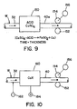
- the two embodiments of the present invention can be manufactured by a variety of manufacturing processes; however, in practice, when the layer 40a is produced with a thickness of less than about 10 microns, wire W is passed through an acid bath 150 as shown in FIGURE 9.
- the bath contains copper sulfate so a chemical reaction occurs wherein copper molecules replace iron molecules on surface 32 as wire w is conveyed through the acid bath 150.
- the conveyor is standard and schematically illustrated as rolls 152, 154 driven at the desired speed by motor 156.
- the speed and chemical concentration determines the thickness of the chemically deposited pure copper on surface 32.
- the resident time in bath 150 controls the thickness of copper layer 40a in accordance with standard manufacturing technology.
- motor 156 operates at the desired speed to control the thickness of layer 40a as it is conveyed through acid bath 150.
- a electrolyte bath 160 contains solution of copper alloy to be deposited on surface 32 to form layer 40 by appropriate electrical connections, shown as a negative terminal 162 and a positive terminal 164.
- the molten metal bath of copper alloy is deposited by electroplating onto surface 32 to produce layer 40.
- the conveyor is illustrated as motor 156 that drives feed rolls 152, 154.
- the motor controls the speed of wire w as it passes through the electrolytic bath 160 for electrically coating the copper alloy onto surface 32.
- the reduced layer 40a of pure copper is created by a chemical reaction, as shown in FIGURE 9.
- the preferred embodiment of the present invention employing copper alloy involves electroplating the alloy onto the moving wire W to produce layer 40, as shown in FIGURE 10.
- the layer can have the same thickness a as the prior art or the reduced dimension b, as discussed in connection with the second embodiment of the invention.
- Various processes can be used for obtaining the desired outer layer for the welding wire W, A representative process producing welding wire is shown in Inoue 6,079,243, incorporated by reference herein for general background.
Landscapes
- Chemical & Material Sciences (AREA)
- Engineering & Computer Science (AREA)
- Organic Chemistry (AREA)
- Chemical Kinetics & Catalysis (AREA)
- Electrochemistry (AREA)
- Materials Engineering (AREA)
- Metallurgy (AREA)
- Mechanical Engineering (AREA)
- Plasma & Fusion (AREA)
- Physics & Mathematics (AREA)
- Arc Welding In General (AREA)
- Nonmetallic Welding Materials (AREA)
- Reciprocating Pumps (AREA)
- External Artificial Organs (AREA)
Abstract
Description
- The present invention relates to the arc welding industry and more particularly to a novel electric arc welding wire having a unique electrically conductive outer layer.
- In electric arc welding of pipe sections, it is normal practice to use one or more electrodes fed through drive rolls into a groove between adjoining pipe sections. The groove is filled with a granular flux for protecting the weld bead formed by the melted electrode and the melted workpieces of the bottom of the groove. The welding process produces a weld bead of molten metal covered by the molten slag formed from granular flux. The electrode, whether solid wire or cored wire, includes an outer layer of copper for facilitating the electrical contact between the steel of the electrode and the power lead from a welding power source. The resistivity of copper is quite low so the wire passing through the contact tip of the welding torch receives current from the contact tip without large heat loss in the torch itself and without arcing between the wire and the contact tip. Consequently, it is very important that the outer layer of the advancing weld metal be copper; however, during the feeding operation the copper layer on the wire often creates flakes and particles of pure copper that are mechanically removed from the surface during the forced feeding of the welding wire through the liner into the torch and through the torch contact tip into the welding operation. These flakes or particles of copper have a substantial mass and commingle with the granular flux covering the welding operation.
- Particles of copper dispersed in the flux are melted by the molten slag and often passes through the molten slag into contact with the weld bead. The bead metal cools and solidifies at approximately 2800°F; however, the copper in the molten slag remains molten and migrates through the slag to the surface of the solidified weld bead. This molten copper as a low surface tension and tends to migrate into the solidified weld metal at the grain boundaries. Copper in the grain boundaries of the weld bead cause subsequent cracking, referred to in the industry as "copper cracking." Copper cracking is a specific example of a generic phenomenon known as liquid metal embrittlement (LME). LME involves cracking of a solid substrate caused by a liquid metal. Copper cracking becomes even more pronounced as the granular flux is reused accumulating greater amounts of copper flakes or particles dispersed through the granular flux. Thus, as flux is reused, there is an increased amount of copper particles to migrate through the molten slag over the top of the solidified weld metal thus increasing the tendency for subsequent copper cracking of the weld metal bead. To reduce this tendency, the welding industry sometimes uses only new granular flux during each pass in the pipe welding process. This is costly and results in a substantial waste of excellent, effective granular flux. Another procedure for reducing copper cracking is to assure no abrasive action against the wire as it is being fed. This requires expensive and frequent attention to refurbishing the total welding equipment often during the use of the equipment for pipe welding. Both of these procedures involve the objective of reducing the amount of copper in the granular flux. They are expensive and time consuming procedures requiring routine and expensive intervention. Also, the use of copper free wire can lead to excessive tip heating and electrical erosion, particularly at the high currents used in pipe welding.
- The present invention relates to an electric arc welding wire having an outer cylindrical surface with an electrically conductive layer on the surface wherein the layer is composed of an alloy that will not lead to LME of the weld metal. In accordance with the primary aspect of the present invention the outer layer comprises an alloy of copper where the cooper content is in the range of 60% to 90% by weight of the alloy. By using a copper alloy, as opposed to essentially pure copper, it has been found that the flaking of the alloy from the outer surface does not cause copper cracking of the weld metal. The copper alloy apparently has higher surface tension and can not migrate into the grain boundaries in the solidified weld metal by capillary action or otherwise. The use of copper alloy, as opposed to pure copper, has been found to drastically reduce the copper cracking of the weld metal, even though the outer layer still produces a low resistivity for performing the electrical connection between the moving wire and the contact tip connected to the power lead of a power source. The substitution of a copper alloy for pure copper as the surface layer for the electrical arc welding wire still produces an effective resistivity greater than 2.0 x 10⁻⁸ ohm-meter at 20°C. "Effective resistivity" is the resistivity value of an alloy where the resistivity of one metal is multiplied by its percentage and added to the resistivity of the second metal multiplied by its percentage. Resistivities of representative metals are:
- Copper 1.67 10-6 ohm-meter at 20°C
- Aluminum 2.69 10-8 ohm-meter at 20°C
- Zinc 5.92 10-8 ohm-meter at 20°C
- Nickel 6.84 10-8 ohm-meter at 20°C
- Cadmium 7.40 10-6 ohm-meter at 20°C
- Tin 12.80 10-8 ohm-meter at 20°C
- Thus the effective resistivity of an alloy with 70% copper and 30% nickel is 3.22. This is about 40-50% the actual resistivity of pure copper.
- A low effective resistivity (2.0-4.0) is accomplished by having a greater portion of the alloy being copper and a lesser portion of the alloy being a higher resistivity material such as nickel, zinc, chromium, cadmium or tin. Preferably, the alloy is copper nickel with about 20-30% nickel and the remainder copper. It has been found that this alloy has a resistivity between 2.0-4.0, but will not penetrate into the grain boundaries of the solidified weld metal even if alloy migrates through the molten slag on the top of the weld bead subsequent to the welding operation.
- In accordance with another aspect of the present invention, the alloy on the welding wire is copper and one or more metal selected from the class consisting of nickel, zinc, chromium, cadmium and tin. In one embodiment, the wire is a cored wire, either metal cored or flux cored, Furthermore, it has been found that the wire with the copper alloy is useful for sub arc welding especially when it is cored wire. The conductive layer is applied onto the surface in accordance with standard procedures. The method of applying the coating can be varied as determined by the manufacture of the novel electrode.
- In accordance with a second embodiment of the invention, the electric arc welding wire has an electrically connected layer on the outer surface which layer has a nominal thickness of less than 0.5 microns with the layer being greater than 99% by weight of copper. This is a small weight as a percentage of the electrode. The preferred thin layer has a controlled thickness in the range of 0.03 to 0.35 microns. Thus, pure copper is still used on the wires; however, the copper available for scraping from the wire is reduced drastically from a relatively thick layer as in the prior art to an ultra-thin layer, such as less than about 0.5 microns. This reduction of layer thickness is a reduction of at least 50% in the amount of copper on the wire. In practice the copper has a thickness in the range of 0.6-1.70 microns, but generally in the range of 0.8-1.2 microns. It has been found that the reduced amount of copper (less than 0.5 microns) still produces the desired electrical characteristics, but decreases the tendency for the outer layer to create a relatively large flakes or particles of pure copper. Thus, any copper coming off the wire during the feeding operation will be extremely small in size with a mass substantially reduced. The copper particles migrating through the molten slag will have a very small tendency to penetrate the solidified weld bead.
- The primary object of the present invention is the provision of an electric arc welding wire having an outer electrically conductive layer that reduces the tendency to produce large particles or flakes of substantially pure copper at the surface of the weld bead.
- A further object of the present invention is the provision of an electric arc welding wire, as defined above, which welding wire has a layer that is formed of an alloy of copper and another metal. By using a copper alloy, the alloy migrating to the weld bead does not penetrate the boundaries of the solidified weld bead as equal sized masses of pure copper.
- Still a further object of the present invention is the provision of an electric arc welding wire having an electrically conductive layer, which layer is formed of substantially pure copper but has a thickness of less than 0.5 microns. In this manner, the available mass of particles removed from the advancing welding wire is not large enough to create a volume of copper sufficient to lead to copper cracking of the weld metal.
- These and other objects and advantages will become apparent from the following description taken together with the accompanying drawings.
-
- FIGURE 1 is a schematic layout of a submerged arc welding system;
- FIGURE 2 is an enlarged cross-sectional view taken generally along line 2-2 of FIGURE 1;
- FIGURE 2A is a cross-sectional view, similar to FIGURE 2, showing a cored electrode as the welding wire;
- FIGURE 3 is a side elevational view illustrating the relationship of the electrode and workpiece with surrounding flux as used in a submerged arc welding process;
- FIGURE 4 is an enlarged cross-sectional view of the prior art illustrating migration or penetration of copper into a grain boundary, when large particles of pure copper are deposited on the outer surface of solidified weld metal during the arc welding process shown in FIGURE 3;
- FIGURE 5 is an enlarged cross-sectional view, similar to FIGURE 4, showing the difference between a pure copper mass on the surface of the solidified weld metal as shown in FIGURE 4 and an alloy of copper used in accordance with the present invention;
- FIGURE 6 is an enlarged partial cross-sectional view taken generally along line 6-6 of FIGURE 2;
- FIGURE 7 is an enlarged cross-sectional view, similar to FIGURE 6, showing one embodiment of the present invention where the amount of pure copper is reduced to decrease the available copper for forming particles or globulars of copper in the molten slag during the welding process as shown in FIGURE 3;
- FIGURE 8 is an enlarged cross-sectional view similar to FIGURE 7 illustrating certain surface irregularities on the outer surface of the welding wire;
- FIGURE 9 is a schematic diagram illustrating the device for reducing the thickness of substantially pure copper as shown in FIGURE 7; and,
- FIGURE 10 is a schematic diagram illustrating the device for electroplating a copper alloy onto the surface of the advancing welding wire.
- The present invention relates primarily to submerged arc welding, schematically illustrated in FIGURE 1 as an AC MIG process using an electric arc welding wire W provided on
reel 10 and pulled from the reel by drive rolls 12, 14. The rolls force wire W throughcontact tip 16 toward workpiece WP where the welding wire W is melted by electric current fromAC power source 20. To perform the welding process,power lead 22 is connected withcontact tip 16 toward workpiece WP. In accordance with standard technology, welding wire W includessolid wire 30 having outercylindrical surface 32 covered bylow resistivity layer 40. In the prior art,layer 40 is essentially pure copper with a resistivity of 1.67 x 10⁻⁸ ohm-meter. The submerged arc welding process is illustrated in more detail in FIGURE 3 wherein welding wire w haslower end 50 facing workpiece WP. Current frompower source 20 creates arc A as electrode or wire W traverses in the direction of the arrow shown in FIGURE 3. The welding process melts metal from workpiece WP and from advancing welding wire W to create a molten metal puddle ultimately solidified to form aweld bead 60. Wire W moves through a large mass ofgranular flux 62 to melt the wire and workpiece to formbead 60. In practice, the welding procedure and mechanism together with other mechanical ablation of the surface of moving wire W creates copper flakes orparticles 70 comprising a mass of themetal forming layer 40. These flakes or particles are relatively large in some instances and accumulate as globules ingranular flux 62 as shown schematically in FIGURE 3. Large particles orflakes 70 from the metal oflayer 40 are masses of pure copper. These masses melt and migrate throughmolten slag 80 inmigration lines 90 representing the molten copper particles ormasses 70 moving through the molten slag. The slag ultimately solidifies at a temperature lower than the solidification temperature of weld metal orbead 60; however, as indicated bymigration line 92, in many instances the copper flakes orparticles 70 actually migrate to and into contact with the weld metal as it is being solidified and forming grains. The result of copper on the surface ofhot bead 60 is illustrated in FIGURE 4 wherein the large mass of copper 70a has migrated throughmolten slag 80 onto the upper surface ofweld bead 60. This phenomenon is the prior art problem to which this invention is directed. On the weld bead, the pure copper of mass 70a has a low surface tension and penetrates intograin boundary 100 ofgrains grain boundary size 100; however, FIGURE 4 schematically illustrates what happens when the molten mass of pure copper migrates throughmolten slag 80 and engagesweld metal bead 60. The pure copper enters the grain boundaries of the solidified weld bead thus reducing the strength of the overall weld to the point where the existing residual stresses will form a crack. This crack is an unacceptable defect. As explained in the introductory portion of this disclosure several techniques have been used to remove the tendency for the copper to accumulate on the surface of the weld bead and cause subsequent copper cracking. The present invention solves this problem in a more efficient, less costly and positive manner. In accordance with the invention,layer 30 is an alloy of copper and the copper constituent is less than 90% by weight of the alloy. In accordance with the invention,layer 40 is an alloy of copper and one or more of the metals selected from the class consisting of nickel, zinc, chromium, cadmium and tin. Of course, other alloying metals can be used so long as the effective resistivity oflayer 40 is less than about 4.0 x 10⁻⁸ ohm-meter. The copper alloy oflayer 40 includes 60-80% copper and 20-40% nickel in the preferred embodiment. With 90% copper, the effective resistivity is approximately 2.2. When the copper is reduced to about 70%, the effective resistivity is increased to about 3.2. Consequently, in accordance with the invention, the effective resistivity of the copper alloy is in the general range of 2.0-4.0. It has been found that the surface tension and other physical characteristics associated with copper alloy is different than the physical action of pure copper, as shown in FIGURE 4. The copper alloy has a major portion of copper and only 10% to about 40% of another metal or metals. When suchcopper alloy mass 70b having the same size as mass or particle 70a in FIGURE 4 accumulates on the surface ofweld metal bead 60, as shown in FIGURE 5, the copper alloy does not migrate into thegrain boundary 100. Thus, the use of a copper alloy, as contemplated by the present invention does not cause subsequent copper cracking of the weld metal as in the prior art. No special mechanical or maintenance procedures are necessary to prevent copper cracking when using a copper alloy with a high percentage of copper as taught by the present invention. - Cored wire W' as shown in FIGURE 2A, can be used to practice the invention. Welding wire W' includes an outer low
carbon metal sheath 120 having acenter core 122. The core can be either a metal core or a flux core.Wire layer 130 is copper alloy as explained in connection with welding wire W. Thus, copper alloy for the outer conductive layer of welding wire can be used for solid wire, as shown in FIGURE 2, or for cored wire as shown in FIGURE 2A. Welding wire W has alayer 40 with a thickness a, as shown in FIGURE 6. The thickness is normal for welding wire and is substantially greater than 1.0 microns and is formed from copper alloy. The novel alloy is such that the actual resistivity is at about 10-80% of the level of pure copper. This provides sufficient conductivity for current used in the welding process. In accordance with the first embodiment of the invention, the thickness a is not changed. Copper alloy forlayers - In accordance with another aspect of the present invention, the mass of each copper flake or
particles 70 influx 62 can be reduced by drastically reducing the thickness oflayer 40 from the dimension a shown in FIGURE 6 to the dimension b shown in FIGURE 7. In accordance with this embodiment of the invention,layer 40a has a thickness b, which is less than 0.50 microns. Preferably the ultra-thin layer is in the range of 0.03 to 0.35 microns. Thus, any flakes or particles ablated from the outer layer of wire W are smaller. Furthermore, with a reduced thickness of the layer, there is a correspondingly reduced tendency to provide copper particles in the flux to cause grain boundary deterioration of the prior art. This second embodiment of the invention is drastic reduction in the thickness of the layer when using pure copper. When using the novel thin layer of pure copper, normal indentations 30a onsurface 32 are filled with the copper oflayer 40a as shown in FIGURE 8. Thus, the thickness b oflayer 40a allows filling of irregularities along the surface to produce a smooth outer surface which has an exposed coating of pure copper without using the normal thickness of copper. Thus, there is less copper to ablate from the surface during the feeding procedure used in the welding process. - The two embodiments of the present invention can be manufactured by a variety of manufacturing processes; however, in practice, when the
layer 40a is produced with a thickness of less than about 10 microns, wire W is passed through anacid bath 150 as shown in FIGURE 9. The bath contains copper sulfate so a chemical reaction occurs wherein copper molecules replace iron molecules onsurface 32 as wire w is conveyed through theacid bath 150. The conveyor is standard and schematically illustrated asrolls motor 156. The speed and chemical concentration determines the thickness of the chemically deposited pure copper onsurface 32. The resident time inbath 150 controls the thickness ofcopper layer 40a in accordance with standard manufacturing technology. Thus,motor 156 operates at the desired speed to control the thickness oflayer 40a as it is conveyed throughacid bath 150. This is the second embodiment of the present invention. The preferred embodiment of the present invention uses the manufacturing process schematically illustrated in FIGURE 10. Aelectrolyte bath 160 contains solution of copper alloy to be deposited onsurface 32 to formlayer 40 by appropriate electrical connections, shown as anegative terminal 162 and apositive terminal 164. The molten metal bath of copper alloy is deposited by electroplating ontosurface 32 to producelayer 40. As in FIGURE 9, the conveyor is illustrated asmotor 156 that drives feed rolls 152, 154. The motor controls the speed of wire w as it passes through theelectrolytic bath 160 for electrically coating the copper alloy ontosurface 32. In practice, the reducedlayer 40a of pure copper is created by a chemical reaction, as shown in FIGURE 9. The preferred embodiment of the present invention employing copper alloy involves electroplating the alloy onto the moving wire W to producelayer 40, as shown in FIGURE 10. The layer can have the same thickness a as the prior art or the reduced dimension b, as discussed in connection with the second embodiment of the invention. Various processes can be used for obtaining the desired outer layer for the welding wire W, A representative process producing welding wire is shown in Inoue 6,079,243, incorporated by reference herein for general background.
Claims (16)
- An electric arc welding wire (W) having an outer surface (32) and an electrically conductive layer (40) on said surface (32), said layer (40) comprising an alloy of copper.
- An electric arc welding wire as defined in claim 1, wherein said outer surface (32) is cylindrical, said alloy of copper having a resistivity in the range of about 2-4 x 10⁻⁸ ohm-meter at 20°C.
- The electric arc welding wire as defined in claim 1 or 2, wherein the copper content of said alloy is up to about 90 weight percent of said alloy, preferably about 60-90 weight percent of said alloy, more preferably about 60-80 weight percent.
- The electric arc welding wire as defined in any one of claims 1 to 3, wherein said alloy includes at least one metal selected from the group consisting of cadmium, chromium, nickel, tin, zinc, or mixtures thereof.
- The electric arc welding wire as defined in any one of claims 1 to 4, wherein said alloy is copper and nickel.
- The electric arc welding wire as defined in any one of claims 1 to 5, wherein said alloy comprises about 60 to 80 percent copper and about 20-40 weight percent nickel.
- The electric arc welding wire as defined in claim 6, wherein said alloy is about 70 weight percent copper and about 30 weight percent nickel.
- The electric arc welding wire as defined in any one of claims 1 to 7, wherein said welding wire (W) is a cored wire.
- An electric arc welding wire having an outer surface (32) and an electrically conductive layer (40a) on said surface (32), said layer having a nominal thickness of less than about 0.6 micron and having a copper content of more than about 99 weight percent copper.
- The electric arc welding wire as defined in any one of claims 1 to 9, wherein said layer (40) is electroplated onto said outer surface (32).
- The electric arc welding wire as defined in any of the claims 1 to 10, wherein said layer (40a) is chemically deposited on said surface (32) by replacement of iron molecules with copper molecules.
- The electric arc welding wire as defined in any one of claims 1 to 11, wherein the effective resistivity of the layer (40) is up to about 4.0 x 10⁻⁸ ohm-meter at 20°C.
- The electric arc welding wire as defined in claim 11, wherein the resistivity of the layer (40) is up to about 3.0 x 10⁻⁸ ohm-meter at 20°C.
- The electric arc welding wire as defined in claim 11 or 12, wherein the resistivity of the layer (40) is at least about 2.0 x 10⁻⁸ ohm-meter at 20°C.
- The electric arc welding wire as defined in any one of claims 1 to 14, wherein said layer (40a) having a thickness of less than about 0.5 micron, preferably said layer (40a) having a thickness of about 0.03 to 0.35 micron.
- Use of the electric arc welding wire as defined in any one of claims 1 to 15 in Alternate-Current-Metal-Inert-Gas-Welding (AC MIG welding).
Priority Applications (1)
| Application Number | Priority Date | Filing Date | Title |
|---|---|---|---|
| PL06026188T PL1813375T3 (en) | 2006-01-25 | 2006-12-18 | Electric arc welding wire with an electrically conductive layer of copper or copper alloy |
Applications Claiming Priority (1)
| Application Number | Priority Date | Filing Date | Title |
|---|---|---|---|
| US11/338,507 US8791389B2 (en) | 2006-01-25 | 2006-01-25 | Electric arc welding wire |
Publications (2)
| Publication Number | Publication Date |
|---|---|
| EP1813375A1 true EP1813375A1 (en) | 2007-08-01 |
| EP1813375B1 EP1813375B1 (en) | 2012-08-01 |
Family
ID=37964824
Family Applications (1)
| Application Number | Title | Priority Date | Filing Date |
|---|---|---|---|
| EP06026188A Revoked EP1813375B1 (en) | 2006-01-25 | 2006-12-18 | Electric arc welding wire with an electrically conductive layer of copper or copper alloy |
Country Status (9)
| Country | Link |
|---|---|
| US (1) | US8791389B2 (en) |
| EP (1) | EP1813375B1 (en) |
| CN (1) | CN101007372B (en) |
| AU (1) | AU2006230731B2 (en) |
| BR (1) | BRPI0700115A (en) |
| CA (2) | CA2761173A1 (en) |
| ES (1) | ES2392831T3 (en) |
| MX (1) | MXPA06013964A (en) |
| PL (1) | PL1813375T3 (en) |
Cited By (1)
| Publication number | Priority date | Publication date | Assignee | Title |
|---|---|---|---|---|
| CN110791156A (en) * | 2019-11-01 | 2020-02-14 | 洛阳双瑞特种合金材料有限公司 | Coating for copper-plating-free seamless flux-cored wire, preparation method and coating process |
Families Citing this family (4)
| Publication number | Priority date | Publication date | Assignee | Title |
|---|---|---|---|---|
| US10646965B2 (en) | 2015-08-11 | 2020-05-12 | Hobart Brothers Llc | Tubular welding wire with a thinner sheath for improved deposition rates |
| CN112292229A (en) * | 2018-03-30 | 2021-01-29 | 霍伯特兄弟有限责任公司 | Tubular welding wire made of copper-coated strip |
| US20230119577A1 (en) * | 2021-10-15 | 2023-04-20 | Lincoln Global, Inc. | High alloy welding wire with copper based coating |
| CN114367743B (en) * | 2022-01-11 | 2024-08-23 | 宝鸡市汇鑫金属复合材料有限公司 | Electric arc and laser coupling regulated titanium-steel gradient structural material and method |
Citations (9)
| Publication number | Priority date | Publication date | Assignee | Title |
|---|---|---|---|---|
| GB926863A (en) * | 1961-07-11 | 1963-05-22 | Anthony George Jacobs | An improved method of carbon contact brazing, welding or soldering |
| US3102827A (en) * | 1960-08-10 | 1963-09-03 | Premier Ind Corp | Welding rod |
| GB956612A (en) * | 1960-11-30 | 1964-04-29 | Boehler & Co Ag Geb | Filler material suitable for use in welding steel, and a process of welding steel ina protective gas |
| US3438755A (en) * | 1966-10-19 | 1969-04-15 | Nat Standard Co | Welding wire |
| GB1571136A (en) * | 1977-06-03 | 1980-07-09 | Premier Ind Corp | Consumable arc-welding electrodes |
| JPS648294A (en) * | 1987-06-27 | 1989-01-12 | Tadao Sakaguchi | Wire plated with copper-nickel alloy |
| JPH0441099A (en) * | 1990-06-08 | 1992-02-12 | Daido Steel Co Ltd | Stainless steel welding wire |
| JP2003094108A (en) * | 2001-09-20 | 2003-04-02 | Sumitomo Rubber Ind Ltd | Method of manufacturing metal wire and metal cord using the metal wire |
| EP1350592A1 (en) * | 2002-03-27 | 2003-10-08 | Kawasaki Steel Corporation | Steel wire for mag welding and mag welding method using the same |
Family Cites Families (20)
| Publication number | Priority date | Publication date | Assignee | Title |
|---|---|---|---|---|
| US2170019A (en) * | 1937-08-11 | 1939-08-22 | Thomas S Gaylord | Method of welding |
| GB1147522A (en) | 1965-07-31 | 1969-04-02 | Nippon Electric Co | A composite metal material to be sealed or brazed |
| CH483290A (en) * | 1966-11-23 | 1969-12-31 | Oerlikon Buehrle Elektroden | Filled welding wire |
| JPS58196196A (en) * | 1982-05-12 | 1983-11-15 | Kobe Steel Ltd | Flux cored wire for arc welding |
| JPS59104291A (en) * | 1982-12-06 | 1984-06-16 | Kobe Steel Ltd | Flux cored wire for gas shielded arc welding |
| JPS62160538A (en) | 1986-01-09 | 1987-07-16 | Canon Inc | Recording device noise protection method |
| JP2591120B2 (en) | 1988-12-01 | 1997-03-19 | 松下電器産業株式会社 | Imaging device |
| CN1035420C (en) * | 1992-08-25 | 1997-07-16 | 马德芳 | Mn-plating welding wire |
| CN2209009Y (en) * | 1994-08-30 | 1995-10-04 | 保定拔丝制钉厂 | Special welding wire for coiled nail |
| US6033764A (en) * | 1994-12-16 | 2000-03-07 | Zecal Corp. | Bumped substrate assembly |
| JP3474393B2 (en) | 1997-03-31 | 2003-12-08 | 日鐵住金溶接工業株式会社 | Manufacturing method of welding wire |
| JP3404264B2 (en) | 1997-09-29 | 2003-05-06 | 株式会社神戸製鋼所 | Solid wire for MAG welding |
| US6061023A (en) | 1997-11-03 | 2000-05-09 | Motorola, Inc. | Method and apparatus for producing wide null antenna patterns |
| US6128729A (en) | 1997-12-16 | 2000-10-03 | Hewlett-Packard Company | Method and system for automatic configuration of network links to attached devices |
| CN2319166Y (en) * | 1998-01-16 | 1999-05-19 | 万长明 | Corrosion resistance steel core copper-plating welding wire |
| JP3071774B1 (en) | 1999-02-25 | 2000-07-31 | 高麗溶接棒ジャパン株式会社 | Solid wire for welding with excellent feedability |
| JP2001287623A (en) | 2000-04-06 | 2001-10-16 | Yoshi Amamiya | Vehicle prohibited from traveling when seat belt is not fastened |
| DE102004010130B4 (en) | 2004-03-02 | 2015-03-05 | Maxam Deutschland Gmbh | Process for the preparation and process for the introduction of a high-viscosity emulsion explosive |
| KR20060001022A (en) | 2004-06-30 | 2006-01-06 | 고려용접봉 주식회사 | Surface-treated oil for welding wire and welding wire surface-treated therefrom |
| KR100626416B1 (en) | 2004-12-03 | 2006-09-20 | 고려용접봉 주식회사 | Plating Wire for Gas Shield Arc Welding |
-
2006
- 2006-01-25 US US11/338,507 patent/US8791389B2/en active Active
- 2006-10-03 CA CA2761173A patent/CA2761173A1/en not_active Abandoned
- 2006-10-03 CA CA2562319A patent/CA2562319C/en not_active Expired - Fee Related
- 2006-10-20 AU AU2006230731A patent/AU2006230731B2/en not_active Ceased
- 2006-11-30 MX MXPA06013964A patent/MXPA06013964A/en active IP Right Grant
- 2006-12-11 CN CN2006101656352A patent/CN101007372B/en not_active Expired - Fee Related
- 2006-12-18 EP EP06026188A patent/EP1813375B1/en not_active Revoked
- 2006-12-18 ES ES06026188T patent/ES2392831T3/en active Active
- 2006-12-18 PL PL06026188T patent/PL1813375T3/en unknown
-
2007
- 2007-01-23 BR BRPI0700115-0A patent/BRPI0700115A/en not_active Application Discontinuation
Patent Citations (9)
| Publication number | Priority date | Publication date | Assignee | Title |
|---|---|---|---|---|
| US3102827A (en) * | 1960-08-10 | 1963-09-03 | Premier Ind Corp | Welding rod |
| GB956612A (en) * | 1960-11-30 | 1964-04-29 | Boehler & Co Ag Geb | Filler material suitable for use in welding steel, and a process of welding steel ina protective gas |
| GB926863A (en) * | 1961-07-11 | 1963-05-22 | Anthony George Jacobs | An improved method of carbon contact brazing, welding or soldering |
| US3438755A (en) * | 1966-10-19 | 1969-04-15 | Nat Standard Co | Welding wire |
| GB1571136A (en) * | 1977-06-03 | 1980-07-09 | Premier Ind Corp | Consumable arc-welding electrodes |
| JPS648294A (en) * | 1987-06-27 | 1989-01-12 | Tadao Sakaguchi | Wire plated with copper-nickel alloy |
| JPH0441099A (en) * | 1990-06-08 | 1992-02-12 | Daido Steel Co Ltd | Stainless steel welding wire |
| JP2003094108A (en) * | 2001-09-20 | 2003-04-02 | Sumitomo Rubber Ind Ltd | Method of manufacturing metal wire and metal cord using the metal wire |
| EP1350592A1 (en) * | 2002-03-27 | 2003-10-08 | Kawasaki Steel Corporation | Steel wire for mag welding and mag welding method using the same |
Cited By (2)
| Publication number | Priority date | Publication date | Assignee | Title |
|---|---|---|---|---|
| CN110791156A (en) * | 2019-11-01 | 2020-02-14 | 洛阳双瑞特种合金材料有限公司 | Coating for copper-plating-free seamless flux-cored wire, preparation method and coating process |
| CN110791156B (en) * | 2019-11-01 | 2021-10-01 | 中国船舶重工集团公司第七二五研究所 | Coating for copper-free seamless flux-cored welding wire, preparation method and coating process |
Also Published As
| Publication number | Publication date |
|---|---|
| CN101007372B (en) | 2011-06-22 |
| ES2392831T3 (en) | 2012-12-14 |
| CA2562319A1 (en) | 2007-07-25 |
| EP1813375B1 (en) | 2012-08-01 |
| US8791389B2 (en) | 2014-07-29 |
| MXPA06013964A (en) | 2008-10-09 |
| AU2006230731A1 (en) | 2007-08-09 |
| PL1813375T3 (en) | 2012-12-31 |
| US20070170152A1 (en) | 2007-07-26 |
| CN101007372A (en) | 2007-08-01 |
| CA2562319C (en) | 2012-11-27 |
| BRPI0700115A (en) | 2007-11-06 |
| AU2006230731B2 (en) | 2009-03-05 |
| CA2761173A1 (en) | 2007-07-25 |
Similar Documents
| Publication | Publication Date | Title |
|---|---|---|
| US20140339201A1 (en) | Flux system to reduce copper cracking | |
| CN103182611B (en) | Flux-cored welding wire for carbon steel and process for arc welding | |
| WO2014022241A2 (en) | Root pass welding solution | |
| EP3188873A1 (en) | Hybrid electroslag cladding | |
| EP1813375B1 (en) | Electric arc welding wire with an electrically conductive layer of copper or copper alloy | |
| US4207454A (en) | Method for electroslag welding of metals | |
| CN1297365C (en) | Submerged arc welding method of parallel double wire or single wire adding metal powder | |
| JP3596723B2 (en) | Two-electrode vertical electrogas arc welding method | |
| CN102084035A (en) | Method of providing electric current taker for support bar, and support bar | |
| JP4707949B2 (en) | Multi-electrode single-sided submerged arc welding method | |
| Farkade et al. | Modification in weld overlay for productivity and corrosion resistance | |
| KR101931140B1 (en) | Method of depositing an overlay material onto a metal surface by means of electroslag strip cladding, with flux having more than 55 wt% caf2; corresponding flux and article with such overlay | |
| JP2005319507A (en) | Multi-electrode single-sided submerged arc welding method | |
| JP2002346787A (en) | Solid wire for pulse MAG welding | |
| JPH0569181A (en) | Steel wire for gas shield arc welding and method of manufacturing the same | |
| EP4584046A1 (en) | Welding electrode with functional coatings | |
| JP2000288735A (en) | Two-electrode vertical electrogas arc welding method excellent in welding workability and appearance of Uranami bead | |
| Mandal | Fusion Welding Methods | |
| Ball | The welding of monel and k-monel | |
| JPH0521674B2 (en) | ||
| EP0034598A1 (en) | Improvements in and relating to electroslag welding | |
| JPH05104280A (en) | Metal cored wire with excellent welding workability | |
| JPS5932234B2 (en) | Vertical welding method | |
| JPS5932235B2 (en) | Vertical welding method |
Legal Events
| Date | Code | Title | Description |
|---|---|---|---|
| PUAI | Public reference made under article 153(3) epc to a published international application that has entered the european phase |
Free format text: ORIGINAL CODE: 0009012 |
|
| AK | Designated contracting states |
Kind code of ref document: A1 Designated state(s): AT BE BG CH CY CZ DE DK EE ES FI FR GB GR HU IE IS IT LI LT LU LV MC NL PL PT RO SE SI SK TR |
|
| AX | Request for extension of the european patent |
Extension state: AL BA HR MK YU |
|
| 17P | Request for examination filed |
Effective date: 20071106 |
|
| 17Q | First examination report despatched |
Effective date: 20071213 |
|
| AKX | Designation fees paid |
Designated state(s): AT BE BG CH CY CZ DE DK EE ES FI FR GB GR HU IE IS IT LI LT LU LV MC NL PL PT RO SE SI SK TR |
|
| GRAP | Despatch of communication of intention to grant a patent |
Free format text: ORIGINAL CODE: EPIDOSNIGR1 |
|
| GRAS | Grant fee paid |
Free format text: ORIGINAL CODE: EPIDOSNIGR3 |
|
| GRAA | (expected) grant |
Free format text: ORIGINAL CODE: 0009210 |
|
| AK | Designated contracting states |
Kind code of ref document: B1 Designated state(s): AT BE BG CH CY CZ DE DK EE ES FI FR GB GR HU IE IS IT LI LT LU LV MC NL PL PT RO SE SI SK TR |
|
| REG | Reference to a national code |
Ref country code: GB Ref legal event code: FG4D Ref country code: DE Ref legal event code: R081 Ref document number: 602006031037 Country of ref document: DE Owner name: LINCOLN GLOBAL, INC., SANTA FE SPRINGS, US Free format text: FORMER OWNER: LINCOLN GLOBAL, INC., CITY OF INDUSTRY, CALIF., US |
|
| REG | Reference to a national code |
Ref country code: CH Ref legal event code: EP Ref country code: AT Ref legal event code: REF Ref document number: 568399 Country of ref document: AT Kind code of ref document: T Effective date: 20120815 |
|
| REG | Reference to a national code |
Ref country code: IE Ref legal event code: FG4D |
|
| REG | Reference to a national code |
Ref country code: DE Ref legal event code: R096 Ref document number: 602006031037 Country of ref document: DE Effective date: 20121011 |
|
| PLBI | Opposition filed |
Free format text: ORIGINAL CODE: 0009260 |
|
| REG | Reference to a national code |
Ref country code: NL Ref legal event code: T3 |
|
| REG | Reference to a national code |
Ref country code: ES Ref legal event code: FG2A Ref document number: 2392831 Country of ref document: ES Kind code of ref document: T3 Effective date: 20121214 |
|
| REG | Reference to a national code |
Ref country code: AT Ref legal event code: MK05 Ref document number: 568399 Country of ref document: AT Kind code of ref document: T Effective date: 20120801 |
|
| 26 | Opposition filed |
Opponent name: AIR LIQUIDE WELDING FRANCE Effective date: 20121121 |
|
| REG | Reference to a national code |
Ref country code: PL Ref legal event code: T3 |
|
| REG | Reference to a national code |
Ref country code: LT Ref legal event code: MG4D Effective date: 20120801 |
|
| PG25 | Lapsed in a contracting state [announced via postgrant information from national office to epo] |
Ref country code: IS Free format text: LAPSE BECAUSE OF FAILURE TO SUBMIT A TRANSLATION OF THE DESCRIPTION OR TO PAY THE FEE WITHIN THE PRESCRIBED TIME-LIMIT Effective date: 20121201 Ref country code: LT Free format text: LAPSE BECAUSE OF FAILURE TO SUBMIT A TRANSLATION OF THE DESCRIPTION OR TO PAY THE FEE WITHIN THE PRESCRIBED TIME-LIMIT Effective date: 20120801 Ref country code: CY Free format text: LAPSE BECAUSE OF FAILURE TO SUBMIT A TRANSLATION OF THE DESCRIPTION OR TO PAY THE FEE WITHIN THE PRESCRIBED TIME-LIMIT Effective date: 20120801 Ref country code: AT Free format text: LAPSE BECAUSE OF FAILURE TO SUBMIT A TRANSLATION OF THE DESCRIPTION OR TO PAY THE FEE WITHIN THE PRESCRIBED TIME-LIMIT Effective date: 20120801 |
|
| REG | Reference to a national code |
Ref country code: DE Ref legal event code: R026 Ref document number: 602006031037 Country of ref document: DE Effective date: 20121121 |
|
| PG25 | Lapsed in a contracting state [announced via postgrant information from national office to epo] |
Ref country code: SI Free format text: LAPSE BECAUSE OF FAILURE TO SUBMIT A TRANSLATION OF THE DESCRIPTION OR TO PAY THE FEE WITHIN THE PRESCRIBED TIME-LIMIT Effective date: 20120801 Ref country code: LV Free format text: LAPSE BECAUSE OF FAILURE TO SUBMIT A TRANSLATION OF THE DESCRIPTION OR TO PAY THE FEE WITHIN THE PRESCRIBED TIME-LIMIT Effective date: 20120801 Ref country code: SE Free format text: LAPSE BECAUSE OF FAILURE TO SUBMIT A TRANSLATION OF THE DESCRIPTION OR TO PAY THE FEE WITHIN THE PRESCRIBED TIME-LIMIT Effective date: 20120801 Ref country code: GR Free format text: LAPSE BECAUSE OF FAILURE TO SUBMIT A TRANSLATION OF THE DESCRIPTION OR TO PAY THE FEE WITHIN THE PRESCRIBED TIME-LIMIT Effective date: 20121102 Ref country code: PT Free format text: LAPSE BECAUSE OF FAILURE TO SUBMIT A TRANSLATION OF THE DESCRIPTION OR TO PAY THE FEE WITHIN THE PRESCRIBED TIME-LIMIT Effective date: 20121203 Ref country code: BE Free format text: LAPSE BECAUSE OF FAILURE TO SUBMIT A TRANSLATION OF THE DESCRIPTION OR TO PAY THE FEE WITHIN THE PRESCRIBED TIME-LIMIT Effective date: 20120801 |
|
| PG25 | Lapsed in a contracting state [announced via postgrant information from national office to epo] |
Ref country code: EE Free format text: LAPSE BECAUSE OF FAILURE TO SUBMIT A TRANSLATION OF THE DESCRIPTION OR TO PAY THE FEE WITHIN THE PRESCRIBED TIME-LIMIT Effective date: 20120801 Ref country code: CZ Free format text: LAPSE BECAUSE OF FAILURE TO SUBMIT A TRANSLATION OF THE DESCRIPTION OR TO PAY THE FEE WITHIN THE PRESCRIBED TIME-LIMIT Effective date: 20120801 Ref country code: RO Free format text: LAPSE BECAUSE OF FAILURE TO SUBMIT A TRANSLATION OF THE DESCRIPTION OR TO PAY THE FEE WITHIN THE PRESCRIBED TIME-LIMIT Effective date: 20120801 Ref country code: DK Free format text: LAPSE BECAUSE OF FAILURE TO SUBMIT A TRANSLATION OF THE DESCRIPTION OR TO PAY THE FEE WITHIN THE PRESCRIBED TIME-LIMIT Effective date: 20120801 |
|
| PG25 | Lapsed in a contracting state [announced via postgrant information from national office to epo] |
Ref country code: SK Free format text: LAPSE BECAUSE OF FAILURE TO SUBMIT A TRANSLATION OF THE DESCRIPTION OR TO PAY THE FEE WITHIN THE PRESCRIBED TIME-LIMIT Effective date: 20120801 |
|
| PLAX | Notice of opposition and request to file observation + time limit sent |
Free format text: ORIGINAL CODE: EPIDOSNOBS2 |
|
| PG25 | Lapsed in a contracting state [announced via postgrant information from national office to epo] |
Ref country code: MC Free format text: LAPSE BECAUSE OF NON-PAYMENT OF DUE FEES Effective date: 20121231 Ref country code: BG Free format text: LAPSE BECAUSE OF FAILURE TO SUBMIT A TRANSLATION OF THE DESCRIPTION OR TO PAY THE FEE WITHIN THE PRESCRIBED TIME-LIMIT Effective date: 20121101 |
|
| REG | Reference to a national code |
Ref country code: CH Ref legal event code: PL |
|
| REG | Reference to a national code |
Ref country code: IE Ref legal event code: MM4A |
|
| PLAF | Information modified related to communication of a notice of opposition and request to file observations + time limit |
Free format text: ORIGINAL CODE: EPIDOSCOBS2 |
|
| PG25 | Lapsed in a contracting state [announced via postgrant information from national office to epo] |
Ref country code: CH Free format text: LAPSE BECAUSE OF NON-PAYMENT OF DUE FEES Effective date: 20121231 Ref country code: LI Free format text: LAPSE BECAUSE OF NON-PAYMENT OF DUE FEES Effective date: 20121231 Ref country code: IE Free format text: LAPSE BECAUSE OF NON-PAYMENT OF DUE FEES Effective date: 20121218 |
|
| PLAF | Information modified related to communication of a notice of opposition and request to file observations + time limit |
Free format text: ORIGINAL CODE: EPIDOSCOBS2 |
|
| PGFP | Annual fee paid to national office [announced via postgrant information from national office to epo] |
Ref country code: GB Payment date: 20131227 Year of fee payment: 8 |
|
| PLBB | Reply of patent proprietor to notice(s) of opposition received |
Free format text: ORIGINAL CODE: EPIDOSNOBS3 |
|
| PGFP | Annual fee paid to national office [announced via postgrant information from national office to epo] |
Ref country code: PL Payment date: 20131204 Year of fee payment: 8 Ref country code: NL Payment date: 20131226 Year of fee payment: 8 Ref country code: IT Payment date: 20131220 Year of fee payment: 8 Ref country code: FI Payment date: 20131230 Year of fee payment: 8 Ref country code: ES Payment date: 20131226 Year of fee payment: 8 Ref country code: FR Payment date: 20131217 Year of fee payment: 8 |
|
| PG25 | Lapsed in a contracting state [announced via postgrant information from national office to epo] |
Ref country code: LU Free format text: LAPSE BECAUSE OF NON-PAYMENT OF DUE FEES Effective date: 20121218 |
|
| PGFP | Annual fee paid to national office [announced via postgrant information from national office to epo] |
Ref country code: TR Payment date: 20121210 Year of fee payment: 7 |
|
| PG25 | Lapsed in a contracting state [announced via postgrant information from national office to epo] |
Ref country code: HU Free format text: LAPSE BECAUSE OF FAILURE TO SUBMIT A TRANSLATION OF THE DESCRIPTION OR TO PAY THE FEE WITHIN THE PRESCRIBED TIME-LIMIT Effective date: 20061218 |
|
| REG | Reference to a national code |
Ref country code: NL Ref legal event code: V1 Effective date: 20150701 |
|
| REG | Reference to a national code |
Ref country code: NL Ref legal event code: V1 Effective date: 20150701 |
|
| PG25 | Lapsed in a contracting state [announced via postgrant information from national office to epo] |
Ref country code: FI Free format text: LAPSE BECAUSE OF NON-PAYMENT OF DUE FEES Effective date: 20141218 |
|
| GBPC | Gb: european patent ceased through non-payment of renewal fee |
Effective date: 20141218 |
|
| REG | Reference to a national code |
Ref country code: FR Ref legal event code: ST Effective date: 20150831 |
|
| PG25 | Lapsed in a contracting state [announced via postgrant information from national office to epo] |
Ref country code: NL Free format text: LAPSE BECAUSE OF NON-PAYMENT OF DUE FEES Effective date: 20150701 |
|
| PG25 | Lapsed in a contracting state [announced via postgrant information from national office to epo] |
Ref country code: GB Free format text: LAPSE BECAUSE OF NON-PAYMENT OF DUE FEES Effective date: 20141218 |
|
| PG25 | Lapsed in a contracting state [announced via postgrant information from national office to epo] |
Ref country code: FR Free format text: LAPSE BECAUSE OF NON-PAYMENT OF DUE FEES Effective date: 20141231 |
|
| PG25 | Lapsed in a contracting state [announced via postgrant information from national office to epo] |
Ref country code: IT Free format text: LAPSE BECAUSE OF NON-PAYMENT OF DUE FEES Effective date: 20141218 |
|
| REG | Reference to a national code |
Ref country code: ES Ref legal event code: FD2A Effective date: 20160126 |
|
| PG25 | Lapsed in a contracting state [announced via postgrant information from national office to epo] |
Ref country code: ES Free format text: LAPSE BECAUSE OF NON-PAYMENT OF DUE FEES Effective date: 20141219 |
|
| PG25 | Lapsed in a contracting state [announced via postgrant information from national office to epo] |
Ref country code: PL Free format text: LAPSE BECAUSE OF NON-PAYMENT OF DUE FEES Effective date: 20141218 |
|
| PLAB | Opposition data, opponent's data or that of the opponent's representative modified |
Free format text: ORIGINAL CODE: 0009299OPPO |
|
| R26 | Opposition filed (corrected) |
Opponent name: AIR LIQUIDE WELDING FRANCE Effective date: 20121121 |
|
| APAH | Appeal reference modified |
Free format text: ORIGINAL CODE: EPIDOSCREFNO |
|
| APBM | Appeal reference recorded |
Free format text: ORIGINAL CODE: EPIDOSNREFNO |
|
| APBP | Date of receipt of notice of appeal recorded |
Free format text: ORIGINAL CODE: EPIDOSNNOA2O |
|
| APBQ | Date of receipt of statement of grounds of appeal recorded |
Free format text: ORIGINAL CODE: EPIDOSNNOA3O |
|
| RAP2 | Party data changed (patent owner data changed or rights of a patent transferred) |
Owner name: LINCOLN GLOBAL, INC. |
|
| PG25 | Lapsed in a contracting state [announced via postgrant information from national office to epo] |
Ref country code: TR Free format text: LAPSE BECAUSE OF NON-PAYMENT OF DUE FEES Effective date: 20141218 |
|
| PLBP | Opposition withdrawn |
Free format text: ORIGINAL CODE: 0009264 |
|
| REG | Reference to a national code |
Ref country code: DE Ref legal event code: R082 Ref document number: 602006031037 Country of ref document: DE Representative=s name: GROSSE, SCHUMACHER, KNAUER, VON HIRSCHHAUSEN, DE Ref country code: DE Ref legal event code: R081 Ref document number: 602006031037 Country of ref document: DE Owner name: LINCOLN GLOBAL, INC., SANTA FE SPRINGS, US Free format text: FORMER OWNER: LINCOLN GLOBAL, INC., CITY OF INDUSTRY, CALIF., US |
|
| APAH | Appeal reference modified |
Free format text: ORIGINAL CODE: EPIDOSCREFNO |
|
| PLAB | Opposition data, opponent's data or that of the opponent's representative modified |
Free format text: ORIGINAL CODE: 0009299OPPO |
|
| APBU | Appeal procedure closed |
Free format text: ORIGINAL CODE: EPIDOSNNOA9O |
|
| PGFP | Annual fee paid to national office [announced via postgrant information from national office to epo] |
Ref country code: DE Payment date: 20201223 Year of fee payment: 15 |
|
| RDAF | Communication despatched that patent is revoked |
Free format text: ORIGINAL CODE: EPIDOSNREV1 |
|
| STAA | Information on the status of an ep patent application or granted ep patent |
Free format text: STATUS: THE PATENT HAS BEEN GRANTED |
|
| REG | Reference to a national code |
Ref country code: DE Ref legal event code: R103 Ref document number: 602006031037 Country of ref document: DE Ref country code: DE Ref legal event code: R064 Ref document number: 602006031037 Country of ref document: DE |
|
| RDAG | Patent revoked |
Free format text: ORIGINAL CODE: 0009271 |
|
| STAA | Information on the status of an ep patent application or granted ep patent |
Free format text: STATUS: PATENT REVOKED |
|
| REG | Reference to a national code |
Ref country code: FI Ref legal event code: MGE |
|
| 27W | Patent revoked |
Effective date: 20211031 |