EP1811816A1 - A protection device for electronic converters, related converter and method - Google Patents
A protection device for electronic converters, related converter and method Download PDFInfo
- Publication number
- EP1811816A1 EP1811816A1 EP06425032A EP06425032A EP1811816A1 EP 1811816 A1 EP1811816 A1 EP 1811816A1 EP 06425032 A EP06425032 A EP 06425032A EP 06425032 A EP06425032 A EP 06425032A EP 1811816 A1 EP1811816 A1 EP 1811816A1
- Authority
- EP
- European Patent Office
- Prior art keywords
- converter
- input signal
- output
- comparator
- vref
- Prior art date
- Legal status (The legal status is an assumption and is not a legal conclusion. Google has not performed a legal analysis and makes no representation as to the accuracy of the status listed.)
- Granted
Links
Images


Classifications
-
- H—ELECTRICITY
- H05—ELECTRIC TECHNIQUES NOT OTHERWISE PROVIDED FOR
- H05B—ELECTRIC HEATING; ELECTRIC LIGHT SOURCES NOT OTHERWISE PROVIDED FOR; CIRCUIT ARRANGEMENTS FOR ELECTRIC LIGHT SOURCES, IN GENERAL
- H05B41/00—Circuit arrangements or apparatus for igniting or operating discharge lamps
- H05B41/14—Circuit arrangements
- H05B41/26—Circuit arrangements in which the lamp is fed by power derived from dc by means of a converter, e.g. by high-voltage dc
- H05B41/28—Circuit arrangements in which the lamp is fed by power derived from dc by means of a converter, e.g. by high-voltage dc using static converters
- H05B41/288—Circuit arrangements in which the lamp is fed by power derived from dc by means of a converter, e.g. by high-voltage dc using static converters with semiconductor devices and specially adapted for lamps without preheating electrodes, e.g. for high-intensity discharge lamps, high-pressure mercury or sodium lamps or low-pressure sodium lamps
- H05B41/292—Arrangements for protecting lamps or circuits against abnormal operating conditions
-
- H—ELECTRICITY
- H05—ELECTRIC TECHNIQUES NOT OTHERWISE PROVIDED FOR
- H05B—ELECTRIC HEATING; ELECTRIC LIGHT SOURCES NOT OTHERWISE PROVIDED FOR; CIRCUIT ARRANGEMENTS FOR ELECTRIC LIGHT SOURCES, IN GENERAL
- H05B39/00—Circuit arrangements or apparatus for operating incandescent light sources
- H05B39/04—Controlling
- H05B39/041—Controlling the light-intensity of the source
- H05B39/044—Controlling the light-intensity of the source continuously
- H05B39/045—Controlling the light-intensity of the source continuously with high-frequency bridge converters
-
- H—ELECTRICITY
- H02—GENERATION; CONVERSION OR DISTRIBUTION OF ELECTRIC POWER
- H02H—EMERGENCY PROTECTIVE CIRCUIT ARRANGEMENTS
- H02H7/00—Emergency protective circuit arrangements specially adapted for specific types of electric machines or apparatus or for sectionalised protection of cable or line systems, and effecting automatic switching in the event of an undesired change from normal working conditions
- H02H7/10—Emergency protective circuit arrangements specially adapted for specific types of electric machines or apparatus or for sectionalised protection of cable or line systems, and effecting automatic switching in the event of an undesired change from normal working conditions for converters; for rectifiers
- H02H7/12—Emergency protective circuit arrangements specially adapted for specific types of electric machines or apparatus or for sectionalised protection of cable or line systems, and effecting automatic switching in the event of an undesired change from normal working conditions for converters; for rectifiers for static converters or rectifiers
- H02H7/122—Emergency protective circuit arrangements specially adapted for specific types of electric machines or apparatus or for sectionalised protection of cable or line systems, and effecting automatic switching in the event of an undesired change from normal working conditions for converters; for rectifiers for static converters or rectifiers for inverters, i.e. dc/ac converters
- H02H7/1227—Emergency protective circuit arrangements specially adapted for specific types of electric machines or apparatus or for sectionalised protection of cable or line systems, and effecting automatic switching in the event of an undesired change from normal working conditions for converters; for rectifiers for static converters or rectifiers for inverters, i.e. dc/ac converters responsive to abnormalities in the output circuit, e.g. short circuit
-
- H—ELECTRICITY
- H05—ELECTRIC TECHNIQUES NOT OTHERWISE PROVIDED FOR
- H05B—ELECTRIC HEATING; ELECTRIC LIGHT SOURCES NOT OTHERWISE PROVIDED FOR; CIRCUIT ARRANGEMENTS FOR ELECTRIC LIGHT SOURCES, IN GENERAL
- H05B41/00—Circuit arrangements or apparatus for igniting or operating discharge lamps
- H05B41/14—Circuit arrangements
- H05B41/26—Circuit arrangements in which the lamp is fed by power derived from dc by means of a converter, e.g. by high-voltage dc
- H05B41/28—Circuit arrangements in which the lamp is fed by power derived from dc by means of a converter, e.g. by high-voltage dc using static converters
- H05B41/282—Circuit arrangements in which the lamp is fed by power derived from dc by means of a converter, e.g. by high-voltage dc using static converters with semiconductor devices
- H05B41/285—Arrangements for protecting lamps or circuits against abnormal operating conditions
-
- H—ELECTRICITY
- H05—ELECTRIC TECHNIQUES NOT OTHERWISE PROVIDED FOR
- H05B—ELECTRIC HEATING; ELECTRIC LIGHT SOURCES NOT OTHERWISE PROVIDED FOR; CIRCUIT ARRANGEMENTS FOR ELECTRIC LIGHT SOURCES, IN GENERAL
- H05B41/00—Circuit arrangements or apparatus for igniting or operating discharge lamps
- H05B41/14—Circuit arrangements
- H05B41/26—Circuit arrangements in which the lamp is fed by power derived from dc by means of a converter, e.g. by high-voltage dc
- H05B41/28—Circuit arrangements in which the lamp is fed by power derived from dc by means of a converter, e.g. by high-voltage dc using static converters
- H05B41/295—Circuit arrangements in which the lamp is fed by power derived from dc by means of a converter, e.g. by high-voltage dc using static converters with semiconductor devices and specially adapted for lamps with preheating electrodes, e.g. for fluorescent lamps
- H05B41/298—Arrangements for protecting lamps or circuits against abnormal operating conditions
-
- Y—GENERAL TAGGING OF NEW TECHNOLOGICAL DEVELOPMENTS; GENERAL TAGGING OF CROSS-SECTIONAL TECHNOLOGIES SPANNING OVER SEVERAL SECTIONS OF THE IPC; TECHNICAL SUBJECTS COVERED BY FORMER USPC CROSS-REFERENCE ART COLLECTIONS [XRACs] AND DIGESTS
- Y02—TECHNOLOGIES OR APPLICATIONS FOR MITIGATION OR ADAPTATION AGAINST CLIMATE CHANGE
- Y02B—CLIMATE CHANGE MITIGATION TECHNOLOGIES RELATED TO BUILDINGS, e.g. HOUSING, HOUSE APPLIANCES OR RELATED END-USER APPLICATIONS
- Y02B20/00—Energy efficient lighting technologies, e.g. halogen lamps or gas discharge lamps
-
- Y—GENERAL TAGGING OF NEW TECHNOLOGICAL DEVELOPMENTS; GENERAL TAGGING OF CROSS-SECTIONAL TECHNOLOGIES SPANNING OVER SEVERAL SECTIONS OF THE IPC; TECHNICAL SUBJECTS COVERED BY FORMER USPC CROSS-REFERENCE ART COLLECTIONS [XRACs] AND DIGESTS
- Y10—TECHNICAL SUBJECTS COVERED BY FORMER USPC
- Y10S—TECHNICAL SUBJECTS COVERED BY FORMER USPC CROSS-REFERENCE ART COLLECTIONS [XRACs] AND DIGESTS
- Y10S323/00—Electricity: power supply or regulation systems
- Y10S323/907—Temperature compensation of semiconductor
Definitions
- the present invention relates to protection devices for electronic converters and was developed with specific attention paid to its possbile use in connection with AC/DC converters for halogen lamps.
- a common topological arrangement adopted for electronic converters is an auto-oscillating half-bridge directly supplied with the output voltage coming from a bridge rectifier.
- the output voltage from the bridge rectifier will be a 100 Hz pulsed voltage.
- Auto-oscillation stops at each zero point of the supply voltage, and a circuit element must periodically re-ignite the half-bridge. This is typically obtained by means of a ignition capacitor; the capacitor is charged until its voltage reaches the gate threshold of a diac and the discharge thus produced causes auto-oscillation to (re)start in the half bridge.
- a number of over-load/over-temperature protection arrangements of the prior art thus include two different and independent stages.
- the former stage includes a heat sensitive component (e.g. a thermal resistor, such as a PTC or a NTC) and acts on the ignition capacitor (only) as a function of the temperature detected by the heat sensitive component.
- the latter stage is dedicated to protection against current overloads and detects, at specific point(s) in the circuit certain electrical signals, signals that may be indicative of an overload condition but are generally independent of the temperature; also the latter stage finally acts onto the ignition capacitor.
- the object of the invention is to provide an improved over-load/over-temperature protection arrangement that is exempt from the disadvantages and drawbacks portrayed in the foregoing.
- a preferred embodiment of the arrangement described herein is thus an AC/AC or DC/AC converter which provides a high frequency, insulated low voltage signal adapted to supply 12 V halogen lamps.
- the arrangement described herein prevents the active components in the Electronic Control Gear (ECG) undesired from reaching high temperatures when a power overload is applied at its output (e.g. due to a wrong installation), or ambient temperature reaches a level higher than a maximum recommended level for operation.
- ECG Electronic Control Gear
- the arrangement described herein operates also when the converter is supplied with a DC voltage and further provides an integrated solution for protection both against over-load and over-temperature.
- the arrangement described herein combines the information related to the temperature and to the load present at the output of the converter and generates a signal adapted to actuate components e.g. to stop the oscillation of the half-bridge; this both in the presence of AC supply and in the presence of DC supply.
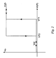
- FIG. 1 shows the "core" of the arrangement described herein. This essentially includes a comparator 10 used in a non-inverting Schmitt-Trigger configuration.
- the inverting input 12 receives a signal Vref(T°) in the form of a continuous, temperature dependent voltage.
- Vref(T°) is selected as a signal (produced as better described in the following) that decreases as the temperature increases.
- the non-inverting input 14 receives a signal Vi(P) in the form of a continuous voltage (produced as better detailed in the following) that is representative of the load, and thus the power, at the output of an associated converter circuit - not shown in figure 1.
- the load-dependent signal Vi(P) is applied to the non-inverting input 14 of the comparator 10 via a resistor R1.
- another resistor R2 Connected to the non-inverting input 14 of the comparator 10 is another resistor R2 that is series-connected to a circuit comprised of a constant voltage source Vb connected in parallel to a diode Do.
- the positive terminal of the source Vb and the cathode of the diode Do are connected to the output of the comparator 10 where an output voltage Vo is present.
- the comparator 10 is powered by means of a single supply voltage Vcc, which is easier to obtain than a double supply +/- Vcc).
- the output voltage Vo from the comparator 10 (ordinate scale) is a two-level signal varying between a low level Vol, typical equal to 0.5 V, and a high level Voh, typically equal to Vcc-1.5V.
- the diagram of figure 2 shows the input-output characteristic of the circuit of figure 1 as a function of the load-dependent signal Vi(P) (abscissa scale). For instance, one may assume that Vi(P) is e.g. proportional (not necessarily directly) to the power at the output of the associated converter.
- the diagram of figure 2 shows a typical hysteresis cycle: above a certain upper limit VT1 for Vi(P) (i.e. too high an output power), the output voltage Vo goes to the high level Voh. The output voltage Vo will then return to the low level Vol only when the signal Vi(P) goes below another, lower value VT2 for Vi(P), with VT2 ⁇ VT1.
- the presence of an overload can be displayed to the user benefit e.g. by the flashing of a lamp prompted by Vo reaching the high level Voh, which is indicative of the presence of abnormal condition.
- VT1 Vref T° * ( 1 + R ⁇ 1 R ⁇ 2 ) - V OL - V ⁇ * R ⁇ 1 R ⁇ 2
- VT2 Vref T° * ( 1 + R ⁇ 1 R ⁇ 2 ) - V OH - Vb * R ⁇ 1 R ⁇ 2 .
- Vb can be adjusted to make the difference (V OH -Vb) very small, thus preventing VT2 from possibly becoming negative or too close to zero. Stated otherwise, the generator Vb ensures that, with the typical voltages present in the circuit, the threshold VT2 will never become negative; in that case, re-ignition of the converter would become impossible.
- the arrangement just described is adapted to implement an over-load (i.e. over-current) protection function due to the presence and the behaviour of the signal Vi(P): if the load becomes too high, the ensuing increase in Vi(P) causes Vo to go to Voh, thus discontinuing operation of the converter.
- over-load i.e. over-current
- the arrangement just described is adapted to implement a thermal (i.e. over-temperature) protection function due to the presence and the behaviour of the signal Vref(T°): if the temperature becomes too high, the ensuing decrease of Vref(T°) causes Vo to go to Voh, thus again discontinuing operation of the converter (since VT1 ⁇ Vi(P)), so that the converter can be switched-off for over-temperature. After this, Vi(P) goes low with a certain time constant and the converter can be re-started. If the temperature is still too high, the converter will work only for a short time before being shut down again.
- a thermal (i.e. over-temperature) protection function due to the presence and the behaviour of the signal Vref(T°): if the temperature becomes too high, the ensuing decrease of Vref(T°) causes Vo to go to Voh, thus again discontinuing operation of the converter (since VT1 ⁇ Vi(P)), so that the converter can be switched-off for over-temperature
- the occurrence of an abnormal condition can be communicated to the user, e.g. by a blinking/flashing light.
- Figure 3 shows the possible application of the protection device described in the foregoing within the framework of a converter that supplies electrical power derived from a power source 20 (e.g. a mains voltage) via a line filter 22 and a half-bridge rectifier 24 to a light source 26 connected to the secondary winding of a transformer Tr.
- the source 26 can be comprised e.g. of one or more halogen lamps, fluorescence lamps, high flux LEDs or the like.
- the primary winding of the transformer Tr having a polarization inductance Lc, is driven via a half-bridge arrangement including:
- the two electronic switches Ta, Tb are alternatively switched on and off by means of a control circuit 38 having associated a Diac 30.
- the Diac 30 is interposed between the gates of the electronic switches Ta, Tb and the intermediate point of a voltage divider comprised of:
- resistor Rd2 is connected to the gate of the electronic switch Tb; the resistor Rd2 is adapted to be connected to ground via a switch Td1.
- the resistor Rds essentially represents the natural resistance that each active component, like a MOSFET or a BJT, shows at its output.
- Both switches Td1 and Td2 are driven by the output voltage Vo of the comparator 10, a protection diode D2 (shown in dashed lines) being preferably provided having its anode connected the output voltage Vo of the comparator 10 and its cathode connected to the control circuit 38.
- the components 10, R1, R2 and Dz form the circuit previously described in connection with figures 1 and 2 whose output Vo is used to de-activate the converter when Vo reaches the value Voh as a result of an anomalous current and/or temperature load being detected.
- FIG 3 the parallel connection of the voltage source Vb and the diode Do of figure 1 (presented as separate components in order to highlight the significance of the parameter Vb and V ⁇ related thereto) has been simply represented in the form a Zener diode VZ having its cathode connected to the output of the comparator 10.
- a Zener diode VZ can in fact be regarded as equivalent to the parallel connection of a voltage source Vb (with Vb being the avalanche voltage of the zener diode) and a diode Do having a forward voltage equal to V ⁇ .
- the circuit formed by the components Rs, Cs and the Diac 30 allows the ignition of the half-bridge at each zero point of the supply voltage.
- the related sensing arrangement includes, in addition to a first resistor Ra1 connected in parallel to the diode Da, a capacitor Cd connected to the secondary winding of the transformer Tr plus a network essentially comprised of two resistors Ra2 and Rb comprising a voltage divider interposed between the capacitor Cd and ground.
- the voltage divider comprised of the resistors Ra2 and Rb scales this ripple signal and feeds it, via a resistor Rc, to a quasi peak-detector network including a diode Dp loading a RC network.
- the RC network includes the parallel connection of a capacitor Cp and a resistor Rd that jointly define the charge and discharge time constants of the detector.
- the continuous voltage across the capacitor Cp is representative of (in fact, proportional to) the load applied at the converter output (i.e. the transformer Tr).
- An op-amp 32 acting as a voltage-follower i.e an impedance separator
- an op-amp 32 acting as a voltage-follower i.e an impedance separator
- Another voltage divider interposed between the supply voltage Vcc and ground includes two resistors R3 and R4 having a NTC (Negative Temperature Coefficient) resistor in parallel to R4 - as shown in full line - and/or a PTC (Positive Temperature Coefficient) resistor in parallel to R3 - as shown in dashed line - to produce the temperature-dependent signal Vref(T°), which decrease with an increase in the temperature.
- NTC Negative Temperature Coefficient
- the fixed resistors R3 and R4 in parallel to the NTC and/or the PTC resistors are intended to linearize the thermal voltage/temperature characteristics of the NTC/PTC resistors and to smoothen out tolerances.
- the resistor Rd2 (and Rd1) represent the natural resistance that an active component, such as a MOSFET or a BJT, shows at its output.
- an active component such as a MOSFET or a BJT
- the impedance is so low that all the current coming from the diac 30 and/or from the inductor Lb flows through the resistor Rd2, in order to avoid bad re-ignition of Tb or malfunctioning of the half-bridge due e.g. to continued operation of the half-bridge with a bad driving of the MOSFET or BJT Tb, with an ensuing risk of self-destruction due to over-heating.
- FIG. 4 shows a possible implementation for the switch Td2. This is essentially constituted by a MOSFET having a relatively high channel resistance, yet able to lead peak current of some hundreds mA. Providing a resistor Rd21 connected in series to the MOSFET Td2 to limit the peak current coming from the capacitor Cs during operation of Td2 (i.e. with Td2 conductive) may be advisable.
- FIG. 5 shows a possible implementation of the switch Td1 when the protection device must operate also with a DC supply for the converter.
- the diode Dd1 is useful in any case in order to avoid that, during normal operation of the half-bridge, the current may undesirably flow through the body-diode of Td1 when the voltage through Lb is negative.
- the resistor Ra1 is essentially a bias resistor that has the role of permitting the re-ignition of the half-bridge, in the case of DC supply voltage, after the switch Td1 is no longer active. In fact, when operation of the half-bridge is discontinued, the coupling capacitor Cb discharges, and ignition of the low-side switch Tb can no longer cooperate with the half-bridge in ramping-up its auto-oscillation.
- the resistor Ra1 conversely ensures that the intermediate point between Ca and Cb remains polarized (at a positive voltage) so that the capacitor Cb always charged.
- Ra1 is not necessary, since a pulsed voltage is in any case present between Ca and Cb. This voltage thus always exhibits some sort of variation over time (i.e. dv/dt), which is sufficient to displace some charge in both capacitors Ca and Cb, so that the intermediate point there between is always (positively) polarized.
Abstract
Description
- The present invention relates to protection devices for electronic converters and was developed with specific attention paid to its possbile use in connection with AC/DC converters for halogen lamps.
- In order to permit electronic converters to properly comply with norms and standards, safety must be preserved even in the presence of abnormal working conditions, i.e., a current load higher than the nominal value applied at the output or an ambient temperature higher than the maximum temperature recommended by the designer. Additionally, automatic restarting of the converter once the abnormal working condition is terminated is a desirable feature.
- A common topological arrangement adopted for electronic converters is an auto-oscillating half-bridge directly supplied with the output voltage coming from a bridge rectifier. For example, in the case of a 50 Hz mains voltage, the output voltage from the bridge rectifier will be a 100 Hz pulsed voltage. Auto-oscillation stops at each zero point of the supply voltage, and a circuit element must periodically re-ignite the half-bridge. This is typically obtained by means of a ignition capacitor; the capacitor is charged until its voltage reaches the gate threshold of a diac and the discharge thus produced causes auto-oscillation to (re)start in the half bridge.
- Most of the over-load/over-temperature protection arrangements proposed so far for such converters include a low impedance path in parallel to the ignition capacitor, so that ignition of the half-bridge becomes impossible. This sort of solution can operate properly only when the converter is supplied with AC voltage. In the presence of a DC supply voltage the ignition of the half-bridge is necessary only when the converter is supplied for the first time; after that, the voltage through the ignition capacitor may remain at any level below the threshold of the diac. In that way, the presence of a low impedance path through in parallel to the ignition capacitor has no impact on operation of the converter. This means that, if the converter is supplied with DC voltage, the protection arrangement does not operate correctly and is not able to guarantee safety as requested.
- A number of over-load/over-temperature protection arrangements of the prior art thus include two different and independent stages. The former stage includes a heat sensitive component (e.g. a thermal resistor, such as a PTC or a NTC) and acts on the ignition capacitor (only) as a function of the temperature detected by the heat sensitive component. The latter stage is dedicated to protection against current overloads and detects, at specific point(s) in the circuit certain electrical signals, signals that may be indicative of an overload condition but are generally independent of the temperature; also the latter stage finally acts onto the ignition capacitor.
- The object of the invention is to provide an improved over-load/over-temperature protection arrangement that is exempt from the disadvantages and drawbacks portrayed in the foregoing.
- According to the present invention, that object is achieved by means of a protection device having the features set forth in the claims that follow. The invention also concerns a related converter and a related method. The claims are an integral part of the disclosure of the invention provided herein.
- A preferred embodiment of the arrangement described herein is thus an AC/AC or DC/AC converter which provides a high frequency, insulated low voltage signal adapted to supply 12 V halogen lamps.
- The arrangement described herein prevents the active components in the Electronic Control Gear (ECG) undesired from reaching high temperatures when a power overload is applied at its output (e.g. due to a wrong installation), or ambient temperature reaches a level higher than a maximum recommended level for operation.
- The arrangement described herein operates also when the converter is supplied with a DC voltage and further provides an integrated solution for protection both against over-load and over-temperature.
- The arrangement described herein combines the information related to the temperature and to the load present at the output of the converter and generates a signal adapted to actuate components e.g. to stop the oscillation of the half-bridge; this both in the presence of AC supply and in the presence of DC supply.
- The invention will now be described, by way of example only, with reference to the enclosed figures of drawing, wherein:
- Figure 1 is a block diagram exemplary of the basic principle underlying the arrangement described herein;
- Figure 2 is a diagram illustrative of operation of the arrangement shown in figure 1;
- Figure 3 is a general block diagram of a converter incorporating the arrangement described herein, and
- Figures 4 and 5 illustrate certain details of a possible embodiment of the arrangement described herein.
- The block diagram of figure 1 shows the "core" of the arrangement described herein. This essentially includes a
comparator 10 used in a non-inverting Schmitt-Trigger configuration. - In this exemplary case, the inverting
input 12 receives a signal Vref(T°) in the form of a continuous, temperature dependent voltage. Preferably Vref(T°) is selected as a signal (produced as better described in the following) that decreases as the temperature increases. - Similarly, in the exemplary case illustrated, the
non-inverting input 14 receives a signal Vi(P) in the form of a continuous voltage (produced as better detailed in the following) that is representative of the load, and thus the power, at the output of an associated converter circuit - not shown in figure 1. - Specifically, the load-dependent signal Vi(P) is applied to the
non-inverting input 14 of thecomparator 10 via a resistor R1. Connected to thenon-inverting input 14 of thecomparator 10 is another resistor R2 that is series-connected to a circuit comprised of a constant voltage source Vb connected in parallel to a diode Do. The positive terminal of the source Vb and the cathode of the diode Do are connected to the output of thecomparator 10 where an output voltage Vo is present. Preferably, thecomparator 10 is powered by means of a single supply voltage Vcc, which is easier to obtain than a double supply +/- Vcc). - As shown in the diagram of figure 2, the output voltage Vo from the comparator 10 (ordinate scale) is a two-level signal varying between a low level Vol, typical equal to 0.5 V, and a high level Voh, typically equal to Vcc-1.5V. Specifically, the diagram of figure 2 shows the input-output characteristic of the circuit of figure 1 as a function of the load-dependent signal Vi(P) (abscissa scale). For instance, one may assume that Vi(P) is e.g. proportional (not necessarily directly) to the power at the output of the associated converter.
- The diagram of figure 2 shows a typical hysteresis cycle: above a certain upper limit VT1 for Vi(P) (i.e. too high an output power), the output voltage Vo goes to the high level Voh. The output voltage Vo will then return to the low level Vol only when the signal Vi(P) goes below another, lower value VT2 for Vi(P), with VT2<VT1.
- The output signal Vo can be used to stop the half-bridge of the associated converter. Specifically, when reaching the high level Voh (because the output power from the associated converter becomes too high), Vo stops - by any known means, that do not require a detailed description herein - operation of the converter and remains in this state (i.e. Vo = Voh) until the absence of output power causes Vi(P) to decrease and fall below the value VT2. At that point, the converter is re-started by Vo at the low level Vol.
- The presence of an overload can be displayed to the user benefit e.g. by the flashing of a lamp prompted by Vo reaching the high level Voh, which is indicative of the presence of abnormal condition.
- Operation of the arrangement illustrated in figure 1 is also dictated by the temperature-dependent signal Vref(T°).
- In fact, circuit analysis of the arrangement illustrated in figure 1 shows that the value for VT1 can be expressed as:

where Vγ is the forward voltage, namely the voltage across the diode Do when the Vo = Vol so that the diode is conducting. This voltage has the opposite direction of the current at the output of thecomparator 10. - Similarly, circuit analysis of the arrangement illustrated in figure 1 shows that the value for VT2 can be expressed as:

- The contribution of Vb is now evident, in that Vb can be adjusted to make the difference (VOH-Vb) very small, thus preventing VT2 from possibly becoming negative or too close to zero. Stated otherwise, the generator Vb ensures that, with the typical voltages present in the circuit, the threshold VT2 will never become negative; in that case, re-ignition of the converter would become impossible.
- The two formulas reported in the foregoing make it clear that the "position" of the hysteresis cycle depends directly on the value of the temperature-dependent signal, namely Vref (T° ) , while the "width" of the hysteresis cycle, that is the difference

- The foregoing highlights a number of basic factors.
- In the first place, the arrangement just described is adapted to implement an over-load (i.e. over-current) protection function due to the presence and the behaviour of the signal Vi(P): if the load becomes too high, the ensuing increase in Vi(P) causes Vo to go to Voh, thus discontinuing operation of the converter.
- In the second place, the arrangement just described is adapted to implement a thermal (i.e. over-temperature) protection function due to the presence and the behaviour of the signal Vref(T°): if the temperature becomes too high, the ensuing decrease of Vref(T°) causes Vo to go to Voh, thus again discontinuing operation of the converter (since VT1<Vi(P)), so that the converter can be switched-off for over-temperature. After this, Vi(P) goes low with a certain time constant and the converter can be re-started. If the temperature is still too high, the converter will work only for a short time before being shut down again.
- In either case considered above, the occurrence of an abnormal condition can be communicated to the user, e.g. by a blinking/flashing light.
- As a further point, it will be appreciated that an increase in the temperature causes a decrease of both VT1 and VT2 together, so that the higher the temperature, the smaller the value of Vi(P) that causes Vo to go to the high level, Voh. Thus the upper operational limit set for over-load protection decreases as the temperature increases; this interdependence ensures that the temperature of the components within the device will never reach values that are too high.
- Figure 3 shows the possible application of the protection device described in the foregoing within the framework of a converter that supplies electrical power derived from a power source 20 (e.g. a mains voltage) via a
line filter 22 and a half-bridge rectifier 24 to alight source 26 connected to the secondary winding of a transformer Tr. Thesource 26 can be comprised e.g. of one or more halogen lamps, fluorescence lamps, high flux LEDs or the like. - In that respect, those of skill in the art will appreciate that the arrangement described herein is adapted for use in connection with any switching converter based on a half-bridge topology. Those of skill in the art will also appreciate that, apart from the details related to the protection device discussed in the foregoing and some specific points mentioned in the following, the block diagram of figure 3 generally corresponds to converter layouts that are per se known from the prior art, thus making it unncessary to provide a more detailed description herein.
- In brief, the primary winding of the transformer Tr, having a polarization inductance Lc, is driven via a half-bridge arrangement including:
- two electronic switches (e.g. MOSFETs or BJTs) Ta, Tb each having an associated gate inductance La, Lb, and
- two capacitors Ca, Cb each having an associated protection diode Da, Db.
- The two electronic switches Ta, Tb are alternatively switched on and off by means of a
control circuit 38 having associated aDiac 30. Essentially, theDiac 30 is interposed between the gates of the electronic switches Ta, Tb and the intermediate point of a voltage divider comprised of: - an "upper" resistor Rs connected to the output of the
rectifier 24, and - a "lower" resistor Rd1 connectable to ground via a switch Td2, a capacitor Cs being connected in parallel to the resitor Rd1.
- Another resistor Rd2 is connected to the gate of the electronic switch Tb; the resistor Rd2 is adapted to be connected to ground via a switch Td1. The resistor Rds essentially represents the natural resistance that each active component, like a MOSFET or a BJT, shows at its output.
- Both switches Td1 and Td2 are driven by the output voltage Vo of the
comparator 10, a protection diode D2 (shown in dashed lines) being preferably provided having its anode connected the output voltage Vo of thecomparator 10 and its cathode connected to thecontrol circuit 38. - The
components 10, R1, R2 and Dz form the circuit previously described in connection with figures 1 and 2 whose output Vo is used to de-activate the converter when Vo reaches the value Voh as a result of an anomalous current and/or temperature load being detected. - In figure 3 the parallel connection of the voltage source Vb and the diode Do of figure 1 (presented as separate components in order to highlight the significance of the parameter Vb and Vγ related thereto) has been simply represented in the form a Zener diode VZ having its cathode connected to the output of the
comparator 10. Such a Zener diode VZ can in fact be regarded as equivalent to the parallel connection of a voltage source Vb (with Vb being the avalanche voltage of the zener diode) and a diode Do having a forward voltage equal to Vγ. - The circuit formed by the components Rs, Cs and the
Diac 30 allows the ignition of the half-bridge at each zero point of the supply voltage. - At the intermediate point between Ca and Cb there is a DC voltage having superimposed thereon a high (oscillation) frequency ripple, whose amplitude depends on the load applied at the converter output.
- This dependence is used to generate the load-dependent signal Vi(P) for feeding the non-inverting input of the
comparator 10. The related sensing arrangement includes, in addition to a first resistor Ra1 connected in parallel to the diode Da, a capacitor Cd connected to the secondary winding of the transformer Tr
plus a network essentially comprised of two resistors Ra2 and Rb comprising a voltage divider interposed between the capacitor Cd and ground. - The function of the resistor Ra1 will be explained in detail in the final part of this description.
- The values of Ra2 and Rb are selected in order to cause the characteristic frequency

- The voltage divider comprised of the resistors Ra2 and Rb scales this ripple signal and feeds it, via a resistor Rc, to a quasi peak-detector network including a diode Dp loading a RC network. The RC network includes the parallel connection of a capacitor Cp and a resistor Rd that jointly define the charge and discharge time constants of the detector.
- As a result, the continuous voltage across the capacitor Cp is representative of (in fact, proportional to) the load applied at the converter output (i.e. the transformer Tr).
- An op-
amp 32 acting as a voltage-follower (i.e an impedance separator) is used to transfer that signal as the signal Vi(P) applied to thecomparator 10. - Another voltage divider interposed between the supply voltage Vcc and ground includes two resistors R3 and R4 having a NTC (Negative Temperature Coefficient) resistor in parallel to R4 - as shown in full line - and/or a PTC (Positive Temperature Coefficient) resistor in parallel to R3 - as shown in dashed line - to produce the temperature-dependent signal Vref(T°), which decrease with an increase in the temperature.
- This specific arrangement is presently preferred over a number of possible alternative arrangements to produce the temperature-dependent signal Vref(T°), which varies as a function of temperature, these possible alternative arrangements including e.g. arrangements adapted to produce signals that increase with an increase in the temperature.
- The fixed resistors R3 and R4 in parallel to the NTC and/or the PTC resistors are intended to linearize the thermal voltage/temperature characteristics of the NTC/PTC resistors and to smoothen out tolerances.
- In the diagram of figure 3, the connections from the output of
comparator 10 to the switches Td1 and Td2 is shown in broken lines to indicate that these connections may be provided at option depending on whether the protection sought is intended to operate only in the presence of an AC supply of the converter or also in the presence of a DC supply respectively. - As indicated, the resistor Rd2 (and Rd1) represent the natural resistance that an active component, such as a MOSFET or a BJT, shows at its output. As described in the introductory portion to this description, if a low impedance path is present in parallel to the capacitor Cs, the half-bridge cannot be re-ignited after the zero of the supply voltage, so that the converter would be stopped.
- This does not apply in the case of DC operation and a low impedance path is created in parallel to the base and emitter of the "low-side" switch Tb, e. g. by switching on, namely closing, the switch Td1.
- Preferably, the impedance is so low that all the current coming from the
diac 30 and/or from the inductor Lb flows through the resistor Rd2, in order to avoid bad re-ignition of Tb or malfunctioning of the half-bridge due e.g. to continued operation of the half-bridge with a bad driving of the MOSFET or BJT Tb, with an ensuing risk of self-destruction due to over-heating. - Figure 4 shows a possible implementation for the switch Td2. This is essentially constituted by a MOSFET having a relatively high channel resistance, yet able to lead peak current of some hundreds mA. Providing a resistor Rd21 connected in series to the MOSFET Td2 to limit the peak current coming from the capacitor Cs during operation of Td2 (i.e. with Td2 conductive) may be advisable.
- Figure 5 shows a possible implementation of the switch Td1 when the protection device must operate also with a DC supply for the converter.
- This again includes a MOSFET Td1 having a very low ohmic channel, for the reasons described before, having associated a diode Dd1. This is a Schottky diode intended to avoid that, when Td1 is switched-on (i.e. is conductive) the total voltage across Td1 and Dd1 may become higher than the threshold voltage Vbe of Tb, so that it can be never stopped. The diode Dd1 is useful in any case in order to avoid that, during normal operation of the half-bridge, the current may undesirably flow through the body-diode of Td1 when the voltage through Lb is negative.
- The resistor Ra1 is essentially a bias resistor that has the role of permitting the re-ignition of the half-bridge, in the case of DC supply voltage, after the switch Td1 is no longer active. In fact, when operation of the half-bridge is discontinued, the coupling capacitor Cb discharges, and ignition of the low-side switch Tb can no longer cooperate with the half-bridge in ramping-up its auto-oscillation. The resistor Ra1 conversely ensures that the intermediate point between Ca and Cb remains polarized (at a positive voltage) so that the capacitor Cb always charged.
- In the case of AC supply, Ra1 is not necessary, since a pulsed voltage is in any case present between Ca and Cb. This voltage thus always exhibits some sort of variation over time (i.e. dv/dt), which is sufficient to displace some charge in both capacitors Ca and Cb, so that the intermediate point there between is always (positively) polarized.
- Consequently, without prejudice to the underlying principles of the invention, the details and the embodiments may vary, even appreciably, with reference to what has been described by way of example only, without departing from the scope of the invention as defined by the annexed claims.
Claims (27)
- A device for protecting an electronic converter, the device including a comparator (10) having an output (Vo) as well as non-inverting (14) and inverting (12) inputs for receiving a first input signal (Vi(P)) indicative of the load applied to said converter and a second input signal (Vref(T°)) indicative of the temperature of said converter, the comparator (10) being in a non-inverting Schmitt-trigger configuration having an input-output characteristic with hysteresis, whereby said output (Vo) is switched from a first value (Vo1) to a second value (Voh) to switch off said electronic converter as said first input signal (Vi(P)) exceeds a first threshold value (VT1) and said output (Vo) is switched back from said second value (Voh) to said first value (Vo1) to restart said electronic converter as said first input signal (Vi(P)) falls below a second threshold value (VT2), said second threshold value (VT2) being lower than said first threshold value (VT1), and both said first (VT1) and second (VT2) threshold values being a function of said second input signal (Vref(T°)).
- The device of claim 1, characterised in that said first input signal (Vi(P)) and said second input signal (Vref(T°)) are applied to said non-inverting (14) and said inverting (12) input of said comparator (10), respectively.
- The device of either of claims 1 or 2, characterised in that said Schmitt-trigger configuration includes a feedback path between said output (Vo) and said non-inverting input (14) of said comparator (10), said feedback path including the parallel connection of a constant voltage source (Vb) and a diode (Do).
- The device of claim 3, characterised in that, in said feedback path, the positive terminal of said constant voltage source (Vb) and the cathode of said diode (Do) are referred to said output (Vo) of said comparator (10).
- The device of either of claims 3 and 4, characterised in that said parallel connection of said constant voltage source (Vb) and said diode (Do) is constituted by a Zener diode.
- The device of any of the previous claims, characterised in that it includes a voltage divider (R1, R2) to apply said first input signal (Vi(P)) to the respective input (14) of said comparator (10).
- The device of claim 6 and any of claims 3 to 5, characterised in that said voltage divider (R1, R2) includes a resistor (R2) included in said feedback path between said output (Vo) and said non-inverting input (14) of said comparator (10).
- The device of any of the previous claims, characterised in that said second input signal (Vref(T°)) decreases as the temperature of said converter increases.
- The device of any of the previous claims, characterised in that it further comprises at least one temperature-sensitive component (NTC, PTC) to produce said second input signal (Vref(T°)) indicative of the temperature of said converter.
- The device of claim 9, characterised in that said temperature-sensitive component includes at least one of a negative temperature coefficient (NTC) and a positive temperature coefficient (PTC) resistor.
- The device of claim 10, characterised in that said at least one of said negative temperature coefficient resistor (NTC) and positive temperature coefficient resistor (PTC) has in parallel thereto a fixed resistor (R3, R4).
- The device of any of claims 9 to 11, characterised in that said temperature-sensitive component (NTC, PTC) is associated to one of the branches of a voltage divider (R3, R4) .
- The device of claim 12, characterised in that said voltage divider (R3, R4) is configured to produce said second input signal (Vref(T°)) at an intermediate point between an upper branch (R3) and a lower branch (R4) of said voltage divider (R3, R4).
- The device of claim 13, characterised in that said temperature-sensitive element is selected out of:- a positive temperature coefficient (PTC) resistor included in the upper branch of said voltage divider, and- a negative temperature coefficient (NTC) resistor included in the lower branch of said voltage divider.
- The device of any of the previous claims, characterised in that it includes ripple sensing circuitry (Cd, Ra2, Rb, Rc, Dp, Cp, Rd) to sense a ripple present on said load (Tr) as said first input signal (Vi(P)) indicative of the load applied to said converter.
- The device of claim 15, wherein said converter includes an half-bridge arrangement having an oscillation frequency imposed thereon, characterised in that said ripple sensing circuitry (Cd, Ra2, Rb, Rc, Dp, Cp, Rd) includes a resonant circuit (Cd, Ra2, Rb) having a characteristic frequency substantially lower than the oscillation frequency imposed on said half-bridge arrangement in said converter.
- The device of either of claims 15 or 16, characterised in that said ripple sensing circuitry (Cd, Ra2, Rb, Rc, Dp, Cp, Rd) includes a quasi peak-detector network (Dp, Rd, Cp) to derive from said ripple on said load (Tr) a substantially continuous signal corresponding to said first input signal (Vi(P)) indicative of the load applied on said converter.
- The device of any of the previous claims, characterised in that it includes at least one switch (Td1, Td2) controlled by said output (Vo) of said comparator (10) to interrupt operation of said converter when said at least one switch (Td1, Td2) is closed.
- The device of claim 18, characterised in that an ignition capacitor (Cs) is provided to ignite said converter and said at least one switch (Td2) is connected to provide a low impedance path (Rd1) in parallel to said ignition capacitor (Cs).
- The device of claim 19, characterised in that said at least one switch (Td2) has a protection resistor (Rd21) connected in series to limit the peak current from said ignition capacitor (Cs) when said at least one electronic switch (Td2) is closed.
- A device according to claim 18, wherein said converter includes a high side electronic switch (Ta) and a low side electronic switch (Tb) alternatively energised to feed said load (Tr), said high-side and low-side electronic switches (Ta, Tb) having respective base and emitter ports, characterised in that said at least one switch (Td1) is configured to create a low-impedance path (Rd2) between the base and the emitter of said low-side electronic switch (Tb).
- The device of claim 21, characterised in that said at least one switch (Td1) has associated a protection diode (Dd1) to prevent the voltage across said at least one switch (Td1) and said protection diode (Dd1) from becoming higher than the threshold voltage of said low-side electronic switch (Tb).
- The device of claim 22, characterised in that said protection diode (Dd1) is a Schottky diode.
- The device of any of the previous claims, wherein said load (Tr) is arranged in a rectifier bridge configuration including two rectifying capacitors (Ca, Cb) having an intermediate point therebetween connected to said load (Tr), characterised in that it includes a bias resistor (Ra1) connected in parallel to one (Ca) of said rectifier capacitors (Ca, Cb).
- An electronic converter including the protection device according to any of claims 1 to 24.
- A method of protecting an electronic converter, the method including the steps of:- generating (Cd, Ra2, Rb, Rc, Dp, Cp, Rd) a first signal (Vi(P)) indicative of the load applied to said converter,- generating (PTC, NTC, R3, Ra) a second signal (Vref(T°) indicative of the temperature of said converter,- providing a comparator (10) having an output (Vo) as well as non-inverting (14) and inverting (12) inputs for receiving a first input signal (Vi(P)) and a second input signal (Vref(T°), the comparator (10) being in a non-inverting Schmitt-trigger configuration having an input-output characteristic with hysteresis, whereby said output (Vo) is switched from a first value (Vo1) to a second value (Voh) as said first input signal (Vi(P)) exceeds a first threshold value (VT1) and said output (Vo) is switched back from said second value (Voh) to said first value (Vo1) as said first input signal (Vi(P)) falls below a second threshold value (VT2), said second threshold value (VT2) being lower than said first threshold value (VT1) and both said first (VT1) and second (VT2) threshold values being a function of said second input signal (Vref(T°)),- applying said first signal (Vi(P)) indicative of the load applied to said converter and said second signal (Vref(T°) indicative of the temperature of said converter to said comparator (10) as said first (Vi(P)) and a second (Vref(T°) input signals,- causing said electronic converter to be switched off and restarted as said output (Vo) of said comparator (10) reaches said first value (Vo1) and said second value (Voh), respectively.
- The method of claim 26, characterised in that it includes the step of generating said second input signal (Vref(T°)) as a singal that decreases as the temperature of said converter increases.
Priority Applications (13)
| Application Number | Priority Date | Filing Date | Title |
|---|---|---|---|
| AT06425032T ATE405137T1 (en) | 2006-01-24 | 2006-01-24 | PROTECTIVE DEVICE FOR ELECTRONIC CONVERTERS, RELATED CONVERTERS AND METHODS |
| DE602006002238T DE602006002238D1 (en) | 2006-01-24 | 2006-01-24 | Protective device for electronic converters, related transducers and methods |
| ES06425032T ES2310898T3 (en) | 2006-01-24 | 2006-01-24 | PROTECTION DEVICE FOR ELECTRONIC CONVERTERS, RELATED CONVERTER AND METHOD. |
| PL06425032T PL1811816T3 (en) | 2006-01-24 | 2006-01-24 | A protection device for electronic converters, related converter and method |
| EP06425032A EP1811816B1 (en) | 2006-01-24 | 2006-01-24 | A protection device for electronic converters, related converter and method |
| AU2007209404A AU2007209404B2 (en) | 2006-01-24 | 2007-01-22 | A protection device for electronic converters, related converter and method |
| US12/087,786 US7965527B2 (en) | 2006-01-24 | 2007-01-22 | Temperature protection device for electronic converters and related method |
| PCT/EP2007/050580 WO2007085580A1 (en) | 2006-01-24 | 2007-01-22 | A protection device for electronic converters, related converter and method |
| CN2007800028128A CN101371621B (en) | 2006-01-24 | 2007-01-22 | A protection device for electronic converters, related converter and method |
| CA002636442A CA2636442A1 (en) | 2006-01-24 | 2007-01-22 | A protection device for electronic converters, related converter and method |
| KR1020087020633A KR101339063B1 (en) | 2006-01-24 | 2007-01-22 | A protection device for electronic converters, related converter and method |
| TW096102291A TW200738066A (en) | 2006-01-24 | 2007-01-22 | A protection device for electronic converters, related converter and method |
| ZA200805276A ZA200805276B (en) | 2006-01-24 | 2008-06-18 | A protection device for electronic converters, related converter and method |
Applications Claiming Priority (1)
| Application Number | Priority Date | Filing Date | Title |
|---|---|---|---|
| EP06425032A EP1811816B1 (en) | 2006-01-24 | 2006-01-24 | A protection device for electronic converters, related converter and method |
Publications (2)
| Publication Number | Publication Date |
|---|---|
| EP1811816A1 true EP1811816A1 (en) | 2007-07-25 |
| EP1811816B1 EP1811816B1 (en) | 2008-08-13 |
Family
ID=36586121
Family Applications (1)
| Application Number | Title | Priority Date | Filing Date |
|---|---|---|---|
| EP06425032A Not-in-force EP1811816B1 (en) | 2006-01-24 | 2006-01-24 | A protection device for electronic converters, related converter and method |
Country Status (12)
| Country | Link |
|---|---|
| US (1) | US7965527B2 (en) |
| EP (1) | EP1811816B1 (en) |
| KR (1) | KR101339063B1 (en) |
| CN (1) | CN101371621B (en) |
| AT (1) | ATE405137T1 (en) |
| CA (1) | CA2636442A1 (en) |
| DE (1) | DE602006002238D1 (en) |
| ES (1) | ES2310898T3 (en) |
| PL (1) | PL1811816T3 (en) |
| TW (1) | TW200738066A (en) |
| WO (1) | WO2007085580A1 (en) |
| ZA (1) | ZA200805276B (en) |
Cited By (3)
| Publication number | Priority date | Publication date | Assignee | Title |
|---|---|---|---|---|
| WO2009122232A1 (en) * | 2008-04-01 | 2009-10-08 | Osram Gesellschaft mit beschränkter Haftung | Improved protection circuit for electronic converters and corresponding method |
| EP2242336A1 (en) * | 2009-04-02 | 2010-10-20 | OSRAM Gesellschaft mit beschränkter Haftung | A converter device for driving light sources, corresponding method and computer program product |
| WO2011066596A3 (en) * | 2009-12-04 | 2011-08-18 | Tridonic Gmbh & Co. Kg | Actuation circuit for an operating device for lighting means |
Families Citing this family (8)
| Publication number | Priority date | Publication date | Assignee | Title |
|---|---|---|---|---|
| US7834561B2 (en) * | 2008-02-01 | 2010-11-16 | Pacific Tech Microelectronics | Systems and methods for powering a light emitting diode lamp |
| US20100156598A1 (en) * | 2008-12-18 | 2010-06-24 | Leung Ting Kwok | Rfid medical devices and systems for reading physiological parameter |
| EP2481267B1 (en) * | 2009-12-04 | 2014-02-12 | OSRAM GmbH | A method for controlling the operation of an electronic converter, and a corresponding electronic converter, lighting system and software product |
| CN201656433U (en) * | 2010-02-05 | 2010-11-24 | 国基电子(上海)有限公司 | Overheat protection circuit and electronic equipment using overheat protection circuit |
| JP5294335B2 (en) * | 2010-06-18 | 2013-09-18 | 三菱電機株式会社 | Semiconductor device |
| GB201309340D0 (en) * | 2013-05-23 | 2013-07-10 | Led Lighting Consultants Ltd | Improvements relating to power adaptors |
| DE102016114384A1 (en) * | 2016-08-03 | 2018-02-08 | Pilz Gmbh & Co. Kg | Protective device for monitoring a technical system with a pressure-sensitive sensor |
| CN110244111B (en) * | 2019-07-19 | 2021-06-29 | 广东浪潮大数据研究有限公司 | Plate-end power supply near-end and far-end voltage detection device |
Citations (1)
| Publication number | Priority date | Publication date | Assignee | Title |
|---|---|---|---|---|
| US6222322B1 (en) | 1997-09-08 | 2001-04-24 | Q Technology Incorporated | Ballast with lamp abnormal sensor and method therefor |
Family Cites Families (6)
| Publication number | Priority date | Publication date | Assignee | Title |
|---|---|---|---|---|
| IT1227586B (en) * | 1988-12-13 | 1991-04-22 | Sgs Thomson Microelectronics | DIAGNOSTIC CIRCUIT FOR CURRENT CONTROL UNIT AND PROTECTION AGAINST EXCESSIVE THERMAL DISSIPATION FOR SEMICONDUCTOR POWER DEVICE |
| CN2221267Y (en) * | 1994-09-24 | 1996-02-28 | 陈为匡 | Device for protecting power semiconductor device |
| US6856098B2 (en) * | 2001-07-02 | 2005-02-15 | Éclairage Contraste | Converter for converting an AC power main voltage to a voltage suitable for driving a lamp |
| DE10245484B4 (en) * | 2002-09-30 | 2004-07-22 | Infineon Technologies Ag | Method for controlling a semiconductor switch and circuit arrangement with a semiconductor switch |
| US20070080905A1 (en) * | 2003-05-07 | 2007-04-12 | Toshiba Matsushita Display Technology Co., Ltd. | El display and its driving method |
| US7149098B1 (en) * | 2006-01-04 | 2006-12-12 | System General Corporation | Over-power protection apparatus with programmable over-current threshold |
-
2006
- 2006-01-24 PL PL06425032T patent/PL1811816T3/en unknown
- 2006-01-24 DE DE602006002238T patent/DE602006002238D1/en active Active
- 2006-01-24 ES ES06425032T patent/ES2310898T3/en active Active
- 2006-01-24 EP EP06425032A patent/EP1811816B1/en not_active Not-in-force
- 2006-01-24 AT AT06425032T patent/ATE405137T1/en not_active IP Right Cessation
-
2007
- 2007-01-22 WO PCT/EP2007/050580 patent/WO2007085580A1/en active Application Filing
- 2007-01-22 TW TW096102291A patent/TW200738066A/en unknown
- 2007-01-22 CN CN2007800028128A patent/CN101371621B/en not_active Expired - Fee Related
- 2007-01-22 KR KR1020087020633A patent/KR101339063B1/en not_active IP Right Cessation
- 2007-01-22 US US12/087,786 patent/US7965527B2/en not_active Expired - Fee Related
- 2007-01-22 CA CA002636442A patent/CA2636442A1/en not_active Abandoned
-
2008
- 2008-06-18 ZA ZA200805276A patent/ZA200805276B/en unknown
Patent Citations (1)
| Publication number | Priority date | Publication date | Assignee | Title |
|---|---|---|---|---|
| US6222322B1 (en) | 1997-09-08 | 2001-04-24 | Q Technology Incorporated | Ballast with lamp abnormal sensor and method therefor |
Non-Patent Citations (3)
| Title |
|---|
| J. MILLMAN, A. GRABEL: "Microelectronics (2nd edition)", 1987, MCGRAW-HILL INTERNATIONAL EDITIONS, SINGAPORE, ISBN: 0-07-100581-1, XP002388164 * |
| J. MILLMAN; A. GRABEL: "Microelectronics", 1987, MCGRAW-HILL |
| PRIETO M J ET AL: "Closing a second feedback low, in DC/DC converters based on piezoelectric 'transformers", POWER ELECTRONICS SPECIALISTS CONFERENCE, 2004. PESC 04. 2004 IEEE 35TH ANNUAL AACHEN, GERMANY 20-25 JUNE 2004, PISCATAWAY, NJ, USA,IEEE, US, 20 June 2004 (2004-06-20), pages 4682 - 4688, XP010739155, ISBN: 0-7803-8399-0 * |
Cited By (5)
| Publication number | Priority date | Publication date | Assignee | Title |
|---|---|---|---|---|
| WO2009122232A1 (en) * | 2008-04-01 | 2009-10-08 | Osram Gesellschaft mit beschränkter Haftung | Improved protection circuit for electronic converters and corresponding method |
| CN101983541A (en) * | 2008-04-01 | 2011-03-02 | 奥斯兰姆有限公司 | Improved protection circuit for electronic converters and corresponding method |
| CN101983541B (en) * | 2008-04-01 | 2013-09-11 | 奥斯兰姆有限公司 | Improved protection circuit for electronic converters and corresponding method |
| EP2242336A1 (en) * | 2009-04-02 | 2010-10-20 | OSRAM Gesellschaft mit beschränkter Haftung | A converter device for driving light sources, corresponding method and computer program product |
| WO2011066596A3 (en) * | 2009-12-04 | 2011-08-18 | Tridonic Gmbh & Co. Kg | Actuation circuit for an operating device for lighting means |
Also Published As
| Publication number | Publication date |
|---|---|
| DE602006002238D1 (en) | 2008-09-25 |
| KR20080096792A (en) | 2008-11-03 |
| KR101339063B1 (en) | 2013-12-09 |
| CA2636442A1 (en) | 2007-08-02 |
| US7965527B2 (en) | 2011-06-21 |
| ZA200805276B (en) | 2009-09-30 |
| ATE405137T1 (en) | 2008-08-15 |
| US20090034307A1 (en) | 2009-02-05 |
| WO2007085580A1 (en) | 2007-08-02 |
| CN101371621A (en) | 2009-02-18 |
| EP1811816B1 (en) | 2008-08-13 |
| TW200738066A (en) | 2007-10-01 |
| PL1811816T3 (en) | 2009-01-30 |
| AU2007209404A1 (en) | 2007-08-02 |
| CN101371621B (en) | 2012-07-18 |
| ES2310898T3 (en) | 2009-01-16 |
Similar Documents
| Publication | Publication Date | Title |
|---|---|---|
| EP1811816B1 (en) | A protection device for electronic converters, related converter and method | |
| JP5266594B1 (en) | LED lamp, lighting device including the LED lamp, and LED lamp current control method | |
| US10320178B2 (en) | Method and apparatus for continuous short-circuit protection | |
| EP1701594B1 (en) | Overload protection arrangement for electronic converters, for instance for halogen lamps | |
| US20070069658A1 (en) | Basic halogen convertor ic | |
| US20140035463A1 (en) | Led lamp and illumination device including the led lamp | |
| US20100060179A1 (en) | Electronic ballast having a partially self-oscillating inverter circuit | |
| JP2004088857A (en) | Input overvoltage protection circuit and electric equipment comprising the same | |
| US5710489A (en) | Overvoltage and thermally protected electronic ballast | |
| US20030031037A1 (en) | Converter for converting an AC power main voltage to a voltage suitable for driving a lamp | |
| MX2012013946A (en) | Led driver protection circuit. | |
| EP0489477A1 (en) | Operating circuit for gas discharge lamps | |
| EP2263422B1 (en) | Electronic converter circuit with improved protection device and corresponding method | |
| AU2007209404B2 (en) | A protection device for electronic converters, related converter and method | |
| US6816393B2 (en) | Switching power supply | |
| JP4706148B2 (en) | Discharge lamp lighting device | |
| JPH1146480A (en) | Switching power supply | |
| CN115136479A (en) | Power supply circuit |
Legal Events
| Date | Code | Title | Description |
|---|---|---|---|
| PUAI | Public reference made under article 153(3) epc to a published international application that has entered the european phase |
Free format text: ORIGINAL CODE: 0009012 |
|
| AK | Designated contracting states |
Kind code of ref document: A1 Designated state(s): AT BE BG CH CY CZ DE DK EE ES FI FR GB GR HU IE IS IT LI LT LU LV MC NL PL PT RO SE SI SK TR |
|
| AX | Request for extension of the european patent |
Extension state: AL BA HR MK YU |
|
| 17P | Request for examination filed |
Effective date: 20071126 |
|
| 17Q | First examination report despatched |
Effective date: 20080107 |
|
| GRAP | Despatch of communication of intention to grant a patent |
Free format text: ORIGINAL CODE: EPIDOSNIGR1 |
|
| AKX | Designation fees paid |
Designated state(s): AT BE BG CH CY CZ DE DK EE ES FI FR GB GR HU IE IS IT LI LT LU LV MC NL PL PT RO SE SI SK TR |
|
| GRAS | Grant fee paid |
Free format text: ORIGINAL CODE: EPIDOSNIGR3 |
|
| GRAA | (expected) grant |
Free format text: ORIGINAL CODE: 0009210 |
|
| AK | Designated contracting states |
Kind code of ref document: B1 Designated state(s): AT BE BG CH CY CZ DE DK EE ES FI FR GB GR HU IE IS IT LI LT LU LV MC NL PL PT RO SE SI SK TR |
|
| REG | Reference to a national code |
Ref country code: GB Ref legal event code: FG4D |
|
| REG | Reference to a national code |
Ref country code: CH Ref legal event code: EP |
|
| REG | Reference to a national code |
Ref country code: IE Ref legal event code: FG4D |
|
| REF | Corresponds to: |
Ref document number: 602006002238 Country of ref document: DE Date of ref document: 20080925 Kind code of ref document: P |
|
| REG | Reference to a national code |
Ref country code: SE Ref legal event code: TRGR |
|
| REG | Reference to a national code |
Ref country code: ES Ref legal event code: FG2A Ref document number: 2310898 Country of ref document: ES Kind code of ref document: T3 |
|
| PG25 | Lapsed in a contracting state [announced via postgrant information from national office to epo] |
Ref country code: IS Free format text: LAPSE BECAUSE OF FAILURE TO SUBMIT A TRANSLATION OF THE DESCRIPTION OR TO PAY THE FEE WITHIN THE PRESCRIBED TIME-LIMIT Effective date: 20081213 Ref country code: NL Free format text: LAPSE BECAUSE OF FAILURE TO SUBMIT A TRANSLATION OF THE DESCRIPTION OR TO PAY THE FEE WITHIN THE PRESCRIBED TIME-LIMIT Effective date: 20080813 Ref country code: LT Free format text: LAPSE BECAUSE OF FAILURE TO SUBMIT A TRANSLATION OF THE DESCRIPTION OR TO PAY THE FEE WITHIN THE PRESCRIBED TIME-LIMIT Effective date: 20080813 |
|
| REG | Reference to a national code |
Ref country code: PL Ref legal event code: T3 |
|
| PG25 | Lapsed in a contracting state [announced via postgrant information from national office to epo] |
Ref country code: SI Free format text: LAPSE BECAUSE OF FAILURE TO SUBMIT A TRANSLATION OF THE DESCRIPTION OR TO PAY THE FEE WITHIN THE PRESCRIBED TIME-LIMIT Effective date: 20080813 Ref country code: LV Free format text: LAPSE BECAUSE OF FAILURE TO SUBMIT A TRANSLATION OF THE DESCRIPTION OR TO PAY THE FEE WITHIN THE PRESCRIBED TIME-LIMIT Effective date: 20080813 Ref country code: AT Free format text: LAPSE BECAUSE OF FAILURE TO SUBMIT A TRANSLATION OF THE DESCRIPTION OR TO PAY THE FEE WITHIN THE PRESCRIBED TIME-LIMIT Effective date: 20080813 Ref country code: FI Free format text: LAPSE BECAUSE OF FAILURE TO SUBMIT A TRANSLATION OF THE DESCRIPTION OR TO PAY THE FEE WITHIN THE PRESCRIBED TIME-LIMIT Effective date: 20080813 |
|
| PG25 | Lapsed in a contracting state [announced via postgrant information from national office to epo] |
Ref country code: BE Free format text: LAPSE BECAUSE OF FAILURE TO SUBMIT A TRANSLATION OF THE DESCRIPTION OR TO PAY THE FEE WITHIN THE PRESCRIBED TIME-LIMIT Effective date: 20080813 |
|
| PG25 | Lapsed in a contracting state [announced via postgrant information from national office to epo] |
Ref country code: DK Free format text: LAPSE BECAUSE OF FAILURE TO SUBMIT A TRANSLATION OF THE DESCRIPTION OR TO PAY THE FEE WITHIN THE PRESCRIBED TIME-LIMIT Effective date: 20080813 Ref country code: BG Free format text: LAPSE BECAUSE OF FAILURE TO SUBMIT A TRANSLATION OF THE DESCRIPTION OR TO PAY THE FEE WITHIN THE PRESCRIBED TIME-LIMIT Effective date: 20081113 |
|
| PG25 | Lapsed in a contracting state [announced via postgrant information from national office to epo] |
Ref country code: CZ Free format text: LAPSE BECAUSE OF FAILURE TO SUBMIT A TRANSLATION OF THE DESCRIPTION OR TO PAY THE FEE WITHIN THE PRESCRIBED TIME-LIMIT Effective date: 20080813 Ref country code: SK Free format text: LAPSE BECAUSE OF FAILURE TO SUBMIT A TRANSLATION OF THE DESCRIPTION OR TO PAY THE FEE WITHIN THE PRESCRIBED TIME-LIMIT Effective date: 20080813 Ref country code: RO Free format text: LAPSE BECAUSE OF FAILURE TO SUBMIT A TRANSLATION OF THE DESCRIPTION OR TO PAY THE FEE WITHIN THE PRESCRIBED TIME-LIMIT Effective date: 20080813 |
|
| PLBE | No opposition filed within time limit |
Free format text: ORIGINAL CODE: 0009261 |
|
| STAA | Information on the status of an ep patent application or granted ep patent |
Free format text: STATUS: NO OPPOSITION FILED WITHIN TIME LIMIT |
|
| 26N | No opposition filed |
Effective date: 20090514 |
|
| PG25 | Lapsed in a contracting state [announced via postgrant information from national office to epo] |
Ref country code: EE Free format text: LAPSE BECAUSE OF FAILURE TO SUBMIT A TRANSLATION OF THE DESCRIPTION OR TO PAY THE FEE WITHIN THE PRESCRIBED TIME-LIMIT Effective date: 20080813 |
|
| PG25 | Lapsed in a contracting state [announced via postgrant information from national office to epo] |
Ref country code: MC Free format text: LAPSE BECAUSE OF NON-PAYMENT OF DUE FEES Effective date: 20090131 |
|
| REG | Reference to a national code |
Ref country code: IE Ref legal event code: MM4A |
|
| PG25 | Lapsed in a contracting state [announced via postgrant information from national office to epo] |
Ref country code: IE Free format text: LAPSE BECAUSE OF NON-PAYMENT OF DUE FEES Effective date: 20090124 |
|
| REG | Reference to a national code |
Ref country code: CH Ref legal event code: PL |
|
| PG25 | Lapsed in a contracting state [announced via postgrant information from national office to epo] |
Ref country code: GR Free format text: LAPSE BECAUSE OF FAILURE TO SUBMIT A TRANSLATION OF THE DESCRIPTION OR TO PAY THE FEE WITHIN THE PRESCRIBED TIME-LIMIT Effective date: 20081114 Ref country code: CH Free format text: LAPSE BECAUSE OF NON-PAYMENT OF DUE FEES Effective date: 20100131 Ref country code: LI Free format text: LAPSE BECAUSE OF NON-PAYMENT OF DUE FEES Effective date: 20100131 |
|
| PG25 | Lapsed in a contracting state [announced via postgrant information from national office to epo] |
Ref country code: LU Free format text: LAPSE BECAUSE OF NON-PAYMENT OF DUE FEES Effective date: 20090124 |
|
| PG25 | Lapsed in a contracting state [announced via postgrant information from national office to epo] |
Ref country code: HU Free format text: LAPSE BECAUSE OF FAILURE TO SUBMIT A TRANSLATION OF THE DESCRIPTION OR TO PAY THE FEE WITHIN THE PRESCRIBED TIME-LIMIT Effective date: 20090214 |
|
| PG25 | Lapsed in a contracting state [announced via postgrant information from national office to epo] |
Ref country code: TR Free format text: LAPSE BECAUSE OF FAILURE TO SUBMIT A TRANSLATION OF THE DESCRIPTION OR TO PAY THE FEE WITHIN THE PRESCRIBED TIME-LIMIT Effective date: 20080813 |
|
| PG25 | Lapsed in a contracting state [announced via postgrant information from national office to epo] |
Ref country code: CY Free format text: LAPSE BECAUSE OF FAILURE TO SUBMIT A TRANSLATION OF THE DESCRIPTION OR TO PAY THE FEE WITHIN THE PRESCRIBED TIME-LIMIT Effective date: 20080813 |
|
| PG25 | Lapsed in a contracting state [announced via postgrant information from national office to epo] |
Ref country code: PT Free format text: LAPSE BECAUSE OF FAILURE TO SUBMIT A TRANSLATION OF THE DESCRIPTION OR TO PAY THE FEE WITHIN THE PRESCRIBED TIME-LIMIT Effective date: 20080813 |
|
| REG | Reference to a national code |
Ref country code: DE Ref legal event code: R081 Ref document number: 602006002238 Country of ref document: DE Owner name: OSRAM GMBH, DE Free format text: FORMER OWNER: OSRAM GESELLSCHAFT MIT BESCHRAENKTER HAFTUNG, 81543 MUENCHEN, DE Effective date: 20111214 |
|
| REG | Reference to a national code |
Ref country code: DE Ref legal event code: R081 Ref document number: 602006002238 Country of ref document: DE Owner name: OSRAM GMBH, DE Free format text: FORMER OWNER: OSRAM AG, 81543 MUENCHEN, DE Effective date: 20130205 |
|
| REG | Reference to a national code |
Ref country code: DE Ref legal event code: R081 Ref document number: 602006002238 Country of ref document: DE Owner name: OSRAM GMBH, DE Free format text: FORMER OWNER: OSRAM GMBH, 81543 MUENCHEN, DE Effective date: 20130823 |
|
| PGFP | Annual fee paid to national office [announced via postgrant information from national office to epo] |
Ref country code: SE Payment date: 20140121 Year of fee payment: 9 |
|
| PGFP | Annual fee paid to national office [announced via postgrant information from national office to epo] |
Ref country code: FR Payment date: 20140123 Year of fee payment: 9 Ref country code: ES Payment date: 20140123 Year of fee payment: 9 |
|
| PGFP | Annual fee paid to national office [announced via postgrant information from national office to epo] |
Ref country code: GB Payment date: 20140121 Year of fee payment: 9 |
|
| PGFP | Annual fee paid to national office [announced via postgrant information from national office to epo] |
Ref country code: PL Payment date: 20141222 Year of fee payment: 10 |
|
| PGFP | Annual fee paid to national office [announced via postgrant information from national office to epo] |
Ref country code: IT Payment date: 20150126 Year of fee payment: 10 |
|
| REG | Reference to a national code |
Ref country code: SE Ref legal event code: EUG |
|
| GBPC | Gb: european patent ceased through non-payment of renewal fee |
Effective date: 20150124 |
|
| PG25 | Lapsed in a contracting state [announced via postgrant information from national office to epo] |
Ref country code: GB Free format text: LAPSE BECAUSE OF NON-PAYMENT OF DUE FEES Effective date: 20150124 |
|
| REG | Reference to a national code |
Ref country code: FR Ref legal event code: ST Effective date: 20150930 |
|
| PG25 | Lapsed in a contracting state [announced via postgrant information from national office to epo] |
Ref country code: SE Free format text: LAPSE BECAUSE OF NON-PAYMENT OF DUE FEES Effective date: 20150125 Ref country code: FR Free format text: LAPSE BECAUSE OF NON-PAYMENT OF DUE FEES Effective date: 20150202 |
|
| REG | Reference to a national code |
Ref country code: ES Ref legal event code: FD2A Effective date: 20160527 |
|
| PG25 | Lapsed in a contracting state [announced via postgrant information from national office to epo] |
Ref country code: ES Free format text: LAPSE BECAUSE OF NON-PAYMENT OF DUE FEES Effective date: 20150125 |
|
| PG25 | Lapsed in a contracting state [announced via postgrant information from national office to epo] |
Ref country code: IT Free format text: LAPSE BECAUSE OF NON-PAYMENT OF DUE FEES Effective date: 20160124 |
|
| PGFP | Annual fee paid to national office [announced via postgrant information from national office to epo] |
Ref country code: DE Payment date: 20170120 Year of fee payment: 12 |
|
| PG25 | Lapsed in a contracting state [announced via postgrant information from national office to epo] |
Ref country code: PL Free format text: LAPSE BECAUSE OF NON-PAYMENT OF DUE FEES Effective date: 20160124 |
|
| REG | Reference to a national code |
Ref country code: DE Ref legal event code: R119 Ref document number: 602006002238 Country of ref document: DE |
|
| PG25 | Lapsed in a contracting state [announced via postgrant information from national office to epo] |
Ref country code: DE Free format text: LAPSE BECAUSE OF NON-PAYMENT OF DUE FEES Effective date: 20180801 |