EP1808692A1 - Biochip, biosensor and inspection system - Google Patents
Biochip, biosensor and inspection system Download PDFInfo
- Publication number
- EP1808692A1 EP1808692A1 EP07000696A EP07000696A EP1808692A1 EP 1808692 A1 EP1808692 A1 EP 1808692A1 EP 07000696 A EP07000696 A EP 07000696A EP 07000696 A EP07000696 A EP 07000696A EP 1808692 A1 EP1808692 A1 EP 1808692A1
- Authority
- EP
- European Patent Office
- Prior art keywords
- biochip
- biosensor
- electrode
- sample solution
- ink
- Prior art date
- Legal status (The legal status is an assumption and is not a legal conclusion. Google has not performed a legal analysis and makes no representation as to the accuracy of the status listed.)
- Withdrawn
Links
- 238000000018 DNA microarray Methods 0.000 title claims abstract description 76
- 238000007689 inspection Methods 0.000 title claims description 12
- 239000010409 thin film Substances 0.000 claims abstract description 18
- 239000012488 sample solution Substances 0.000 claims description 31
- 238000000034 method Methods 0.000 claims description 8
- 238000003860 storage Methods 0.000 claims description 6
- 238000007599 discharging Methods 0.000 claims description 4
- 239000000758 substrate Substances 0.000 description 22
- 239000010410 layer Substances 0.000 description 16
- 238000004458 analytical method Methods 0.000 description 9
- 238000010586 diagram Methods 0.000 description 7
- 239000004033 plastic Substances 0.000 description 7
- 238000004519 manufacturing process Methods 0.000 description 6
- 108090000790 Enzymes Proteins 0.000 description 5
- 102000004190 Enzymes Human genes 0.000 description 5
- VYPSYNLAJGMNEJ-UHFFFAOYSA-N Silicium dioxide Chemical compound O=[Si]=O VYPSYNLAJGMNEJ-UHFFFAOYSA-N 0.000 description 5
- 238000006243 chemical reaction Methods 0.000 description 5
- 229940088598 enzyme Drugs 0.000 description 5
- 239000011521 glass Substances 0.000 description 5
- PCHJSUWPFVWCPO-UHFFFAOYSA-N gold Chemical compound [Au] PCHJSUWPFVWCPO-UHFFFAOYSA-N 0.000 description 5
- 239000010931 gold Substances 0.000 description 5
- 229910052737 gold Inorganic materials 0.000 description 5
- 239000002094 self assembled monolayer Substances 0.000 description 5
- 239000013545 self-assembled monolayer Substances 0.000 description 5
- 108010050375 Glucose 1-Dehydrogenase Proteins 0.000 description 4
- XUIMIQQOPSSXEZ-UHFFFAOYSA-N Silicon Chemical compound [Si] XUIMIQQOPSSXEZ-UHFFFAOYSA-N 0.000 description 4
- 239000000853 adhesive Substances 0.000 description 4
- 230000001070 adhesive effect Effects 0.000 description 4
- 239000010408 film Substances 0.000 description 4
- 239000007788 liquid Substances 0.000 description 4
- 239000000463 material Substances 0.000 description 4
- 108090000623 proteins and genes Proteins 0.000 description 4
- 229910052710 silicon Inorganic materials 0.000 description 4
- 239000010703 silicon Substances 0.000 description 4
- LYCAIKOWRPUZTN-UHFFFAOYSA-N Ethylene glycol Chemical compound OCCO LYCAIKOWRPUZTN-UHFFFAOYSA-N 0.000 description 3
- WQZGKKKJIJFFOK-GASJEMHNSA-N Glucose Natural products OC[C@H]1OC(O)[C@H](O)[C@@H](O)[C@@H]1O WQZGKKKJIJFFOK-GASJEMHNSA-N 0.000 description 3
- 238000005842 biochemical reaction Methods 0.000 description 3
- 239000008103 glucose Substances 0.000 description 3
- 102000004169 proteins and genes Human genes 0.000 description 3
- 239000010453 quartz Substances 0.000 description 3
- 108010015776 Glucose oxidase Proteins 0.000 description 2
- 239000004366 Glucose oxidase Substances 0.000 description 2
- 239000004695 Polyether sulfone Substances 0.000 description 2
- 238000001514 detection method Methods 0.000 description 2
- 238000005516 engineering process Methods 0.000 description 2
- 238000005530 etching Methods 0.000 description 2
- 229940116332 glucose oxidase Drugs 0.000 description 2
- 235000019420 glucose oxidase Nutrition 0.000 description 2
- 230000010354 integration Effects 0.000 description 2
- 238000005259 measurement Methods 0.000 description 2
- 239000000203 mixture Substances 0.000 description 2
- 229920006393 polyether sulfone Polymers 0.000 description 2
- 238000007639 printing Methods 0.000 description 2
- 238000007650 screen-printing Methods 0.000 description 2
- OKTJSMMVPCPJKN-UHFFFAOYSA-N Carbon Chemical compound [C] OKTJSMMVPCPJKN-UHFFFAOYSA-N 0.000 description 1
- SXRSQZLOMIGNAQ-UHFFFAOYSA-N Glutaraldehyde Chemical compound O=CCCCC=O SXRSQZLOMIGNAQ-UHFFFAOYSA-N 0.000 description 1
- VAYOSLLFUXYJDT-RDTXWAMCSA-N Lysergic acid diethylamide Chemical compound C1=CC(C=2[C@H](N(C)C[C@@H](C=2)C(=O)N(CC)CC)C2)=C3C2=CNC3=C1 VAYOSLLFUXYJDT-RDTXWAMCSA-N 0.000 description 1
- 229910021607 Silver chloride Inorganic materials 0.000 description 1
- 125000003277 amino group Chemical group 0.000 description 1
- 229910021417 amorphous silicon Inorganic materials 0.000 description 1
- 239000008280 blood Substances 0.000 description 1
- 210000004369 blood Anatomy 0.000 description 1
- 210000001124 body fluid Anatomy 0.000 description 1
- 239000010839 body fluid Substances 0.000 description 1
- 229910052799 carbon Inorganic materials 0.000 description 1
- 238000004140 cleaning Methods 0.000 description 1
- 229910052681 coesite Inorganic materials 0.000 description 1
- 229910052906 cristobalite Inorganic materials 0.000 description 1
- GPRSOIDYHMXAGW-UHFFFAOYSA-N cyclopenta-1,3-diene cyclopentanecarboxylic acid iron Chemical compound [CH-]1[CH-][CH-][C-]([CH-]1)C(=O)O.[CH-]1C=CC=C1.[Fe] GPRSOIDYHMXAGW-UHFFFAOYSA-N 0.000 description 1
- 238000006073 displacement reaction Methods 0.000 description 1
- 230000036267 drug metabolism Effects 0.000 description 1
- 238000006911 enzymatic reaction Methods 0.000 description 1
- 238000011156 evaluation Methods 0.000 description 1
- 239000012530 fluid Substances 0.000 description 1
- 230000003100 immobilizing effect Effects 0.000 description 1
- AMGQUBHHOARCQH-UHFFFAOYSA-N indium;oxotin Chemical compound [In].[Sn]=O AMGQUBHHOARCQH-UHFFFAOYSA-N 0.000 description 1
- 230000001678 irradiating effect Effects 0.000 description 1
- 238000000608 laser ablation Methods 0.000 description 1
- 238000005224 laser annealing Methods 0.000 description 1
- 238000000691 measurement method Methods 0.000 description 1
- 238000002156 mixing Methods 0.000 description 1
- 238000012544 monitoring process Methods 0.000 description 1
- 238000007254 oxidation reaction Methods 0.000 description 1
- 238000000059 patterning Methods 0.000 description 1
- 229910021420 polycrystalline silicon Inorganic materials 0.000 description 1
- 229920000642 polymer Polymers 0.000 description 1
- 238000000083 pulse voltammetry Methods 0.000 description 1
- 238000005096 rolling process Methods 0.000 description 1
- 239000000377 silicon dioxide Substances 0.000 description 1
- HKZLPVFGJNLROG-UHFFFAOYSA-M silver monochloride Chemical compound [Cl-].[Ag+] HKZLPVFGJNLROG-UHFFFAOYSA-M 0.000 description 1
- 229910052682 stishovite Inorganic materials 0.000 description 1
- 239000000126 substance Substances 0.000 description 1
- 238000010408 sweeping Methods 0.000 description 1
- 125000003396 thiol group Chemical class [H]S* 0.000 description 1
- 238000012546 transfer Methods 0.000 description 1
- 229910052905 tridymite Inorganic materials 0.000 description 1
Images


Classifications
-
- G—PHYSICS
- G01—MEASURING; TESTING
- G01N—INVESTIGATING OR ANALYSING MATERIALS BY DETERMINING THEIR CHEMICAL OR PHYSICAL PROPERTIES
- G01N27/00—Investigating or analysing materials by the use of electric, electrochemical, or magnetic means
- G01N27/26—Investigating or analysing materials by the use of electric, electrochemical, or magnetic means by investigating electrochemical variables; by using electrolysis or electrophoresis
- G01N27/403—Cells and electrode assemblies
- G01N27/414—Ion-sensitive or chemical field-effect transistors, i.e. ISFETS or CHEMFETS
- G01N27/4145—Ion-sensitive or chemical field-effect transistors, i.e. ISFETS or CHEMFETS specially adapted for biomolecules, e.g. gate electrode with immobilised receptors
-
- B—PERFORMING OPERATIONS; TRANSPORTING
- B82—NANOTECHNOLOGY
- B82Y—SPECIFIC USES OR APPLICATIONS OF NANOSTRUCTURES; MEASUREMENT OR ANALYSIS OF NANOSTRUCTURES; MANUFACTURE OR TREATMENT OF NANOSTRUCTURES
- B82Y15/00—Nanotechnology for interacting, sensing or actuating, e.g. quantum dots as markers in protein assays or molecular motors
-
- B—PERFORMING OPERATIONS; TRANSPORTING
- B82—NANOTECHNOLOGY
- B82Y—SPECIFIC USES OR APPLICATIONS OF NANOSTRUCTURES; MEASUREMENT OR ANALYSIS OF NANOSTRUCTURES; MANUFACTURE OR TREATMENT OF NANOSTRUCTURES
- B82Y30/00—Nanotechnology for materials or surface science, e.g. nanocomposites
Definitions
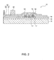
- Fig. 2 is a partial cross section of the biochip 10.
- the biochip .10 includes the plastic substrate 15, an undercoat layer 16 laminated on the above, a source/ drain regions 17 provided on the above, an insulating film 18, a gate electrode 19, a gate insulating film 52, a wiring layer 53, and a thin film transistor 75 formed with an insulating layer 54.
- the biochip 10 includes a plurality of wells 62 forming a concave portion to store a sample solution and a plurality of sensing electrodes 12 provided within each concave portion.
- Figs. 4A through 4G are an example of a manufacturing process of a biochip 10.
- the present manufacturing example uses SUFTLA (Surface Free Technology by Laser Ablation/ Annealing) technology (registered trademark) which fabricates a low-temperature polycrystalline Si TFT on a plastic substrate by using a transfer process.
- SUFTLA Surface Free Technology by Laser Ablation/ Annealing
- the biochip 210 is in a circular-form and the plurality of sensing electrodes 212 are disposed along a circumference, even when many extended wirings as three wirings 262 are extending from each electrode pad 261, the sensing electrode 212 can be mounted on a substrate efficiently and high in integration. Further, as in the case of the second embodiment, because a disk rotation and a discharge of the biochip 210 are time synchronously controlled while sample solution is supplied to the biochip 210, the sample solution can be supplied and detected efficiently.
- GOx glucose oxidase
Landscapes
- Chemical & Material Sciences (AREA)
- Engineering & Computer Science (AREA)
- Health & Medical Sciences (AREA)
- Life Sciences & Earth Sciences (AREA)
- Nanotechnology (AREA)
- Physics & Mathematics (AREA)
- Molecular Biology (AREA)
- Crystallography & Structural Chemistry (AREA)
- General Physics & Mathematics (AREA)
- General Health & Medical Sciences (AREA)
- Analytical Chemistry (AREA)
- Biochemistry (AREA)
- Electrochemistry (AREA)
- Chemical Kinetics & Catalysis (AREA)
- Immunology (AREA)
- Pathology (AREA)
- Composite Materials (AREA)
- Condensed Matter Physics & Semiconductors (AREA)
- Materials Engineering (AREA)
- Microelectronics & Electronic Packaging (AREA)
- Spectroscopy & Molecular Physics (AREA)
- Apparatus Associated With Microorganisms And Enzymes (AREA)
- Automatic Analysis And Handling Materials Therefor (AREA)
Abstract
Description
- The present invention relates to a biochip, a biosensor and an inspection system. More particularly, the present invention relates to a biochip, a biosensor and an inspection system which can realize a micro device that is light, thin, short and compact in size, as well as high in performance and low in cost.
- Various methods are developed to inspect biologically-relevant materials such as DNA and protein to diagnose illness, detect individual difference in drug metabolism, and monitoring food, environment and the like.
- For example, a gene detection chip comprising a pin electrode (refer to a first example of related art) and a protein analysis chip capable of detecting electrical signals (refer to a second example of related art) have been proposed.
Also, a manufacturing method of a biosensor providing an enzyme-immobilized film by forming and immobilizing an enzyme film so as to deposit a polymer solution including a predetermined enzyme ejected from a nozzle to a surface of a predetermined sensor portion has been proposed (refer to a third example of related art).
Further, a manufacturing method of a sensor device forming high-density microelectrodes by printing a thin-film material solution on a microelectrode surface in microdots from an ink-jet nozzle has been proposed (refer to a forth example of related art). -
JP-A-2001-242135 -
JP-A- 2004-20238 -
JP-A-S61-245051 -
JP-A-2000-33712 - However, although various analysis chips and biosensors have been proposed as above, a micro device which can realize a high performance detection and inspection, light, thin, short and compact in size, and also low in cost was not proposed.
- The advantage of the present invention is to provide a biochip, a biosensor, and an inspection system which can realize a biosensing device that is light, thin, short and compact in size, as well as high in performance and low in cost.
- With keen examination, those skilled in the art of the present invention has discovered to realize a biosensing device that is light, thin, short and compact in size, as well as high in performance and low in cost by adopting a predetermined biochip and/or a predetermined biosensor and completed the invention.
- More specifically, the present invention includes a biochip detachably mountable to a biosensor and comprising a sensing electrode being formed with a work electrode, a reference electrode; and a counter electrode, and a thin film transistor; The biochip may further include a well forming a concave portion to store a sample solution; and the sensing electrode may be provided within the concave portion; The biochip may also be circular in form; and a plurality of sensing electrodes may be provided which may be formed with a work electrode, a reference electrode and a counter electrode being disposed along a circumference. The invention also includes a biosensor comprising a storage portion for storing a detachably mountable biochip; an ink-jet head portion for discharging a sample solution by an ink-jet method; a controller which may optionally be provided for controlling a discharge of liquid droplets from a nozzle, together with a memory for accumulating analysis data of a biochip and a drive battery; the ink-jet head portion including a cavity where a sample solution is supplied; a supply portion supplying the sample solution to the cavity; a plurality of nozzles communicated to the cavity and disposed corresponding to each sensing electrode of the biochip when it is mounted in the storing portion; and a main body of a biosensor detachably mountable thereto. The biosensor may further include a circuit board for RF tag. The invention also relates to an inspection system including a biochip or a biosensor as described above.
- The present invention can provide a biochip, a biosensor and an inspection system that is light, thin, short and compact in size, as well as high in performance and low in cost.
- The invention will be described with reference to the accompanying drawings, wherein like numbers reference like elements.
- Fig. 1 is a diagram showing a relationship between a biochip and a biosensor according to a first embodiment.
- Fig. 2 is a partial cross section of the biochip according to the first embodiment.
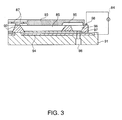
- Fig. 3 is a schematic cross section of an ink-jet head portion of the biosensor according to the first embodiment.
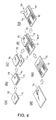
- Figs. 4A through 4G are diagrams showing an example of a manufacturing process of a biochip.
- Fig. 5 is a diagram showing a relationship between a biochip and a biosensor according to a second embodiment.
- Fig. 6 is a diagram showing a biochip according to a third embodiment.
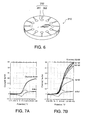
- Figs. 7A and 7B are examples showing a relationship between potential and current value.
- Next, embodiments of the present invention will now be described. Following embodiments are examples to explain the present invention and the invention is not limited only to the embodiments. The present invention may be practiced in various embodiments as long as they do not depart from the scope of the invention.
- A biochip of the present invention includes an ink-jet head portion detachably mountable to a biosensor, a sensing electrode formed with a work electrode, a reference electrode and a counter electrode, and a thin film transistor.
- Fig. 1 is a diagram showing a relationship between a biochip and a biosensor according to a first embodiment. As shown in Fig. 1, a
biochip 10 is detachably mountable to abiosensor 20 and includes aplastic substrate 15, a plurality ofsensing electrodes 12 formed on the above, and a thin film transistor (TFT) 75. - Fig. 2 is a partial cross section of the
biochip 10. As shown in Fig. 2, the biochip .10 includes theplastic substrate 15, anundercoat layer 16 laminated on the above, a source/drain regions 17 provided on the above, aninsulating film 18, agate electrode 19, agate insulating film 52, awiring layer 53, and athin film transistor 75 formed with aninsulating layer 54. Further, thebiochip 10 includes a plurality ofwells 62 forming a concave portion to store a sample solution and a plurality ofsensing electrodes 12 provided within each concave portion.
Thesensing electrode 12 includes three wirings (not shown) of a work electrode (gold, for example), a reference electrode (Ag/AgCl, for example) and a counter electrode (carbon, for example), and anelectrode pad 61 which takes out the wirings. The three wirings are provided in thewiring layer 53 and communicated to thethin film transistor 75 mounted on thebiochip 10. - On a surface of the
electrode pad 61, a biochemical reaction field is established so that specific reactions would take place efficiently to a living organism. Different kinds of biochemical reaction molecules may be fixed on a respective surface of eachelectrode pad 61, so as to monitor different biochemical reactions in parallel. - The above configuration can realize a biosensing device that is light, thin, short and compact in size, as well as high in performance and low in cost.
Further, as the biochip of the present invention is detachably mountable to the biosensor and low in cost, it may be used for disposables and for re-use. - A biosensor of the present invention includes at least a storage portion storing a detachably mountable biochip, an ink-jet head portion discharging a sample solution by an ink-jet method, a controller controlling liquid droplets discharging from a nozzle, a memory accumulating analysis data of the biochip, a drive battery, and the ink-jet head portion having a cavity where a sample solution is supplied, a supply portion supplying the sample solution to the cavity, a plurality of nozzles communicated to the cavity and disposed corresponding to each sensing electrode of the biochip, and a main body of the biosensor detachably mountable thereto.
- As shown in Fig. 1, a
biosensor 20 includes amain body 83 of a biosensor having astorage portion 81 storing a detachablymountable biochip 10, an ink-jet head portion 82 detachably mountable to themain body 83, a controller (not shown) provided in themain body 83 and controls discharge of liquid droplets from the ink-jet head portion 82, a memory (not shown) accumulating analysis data of the biochip, adrive battery 22, acircuit board 21 for RF tag and asupply portion 86 for a sample solution.
Thedrive battery 22 may be a solar battery or a hydrogen-powered battery. The memory, for example, is a flash memory. - Fig. 3 is a schematic cross-section of the ink-
jet head portion 82. The ink-jet head portion 82 has a head structure called SEAJet (registered trademark) and can discharge a sample solution on demand by applying a voltage between electrodes using an electrostatically actuating method.
As shown in Fig. 3, the ink-jet head portion 82 includes acavity 85 where a sample solution is supplied, thesupply portion 86 supplying a sample solution to thecavity 85, 128 pieces ofnozzles 87, aglass substrate 91, asilicon cavity substrate 92 including acavity 85 and avibrating plate 97, and asilicon nozzle substrate 93 including thenozzle 87. Eachsubstrate - The vibrating
plate 97 is provided under thesilicon cavity substrate 92, a fixed-depth concave portion is formed at a surface of theglass substrate 91 at a portion opposing to the vibratingplate 97, and an individual electrode 94 (indium tin oxide) is formed at a bottom of the concave portion. Thevibrating plate 97 corresponding to theindividual electrode 94 is opposed with a fixed gap.
128 pieces ofnozzles 87 are disposed corresponding to eachsensing electrode 12 of thebiochip 10, and communicated to thecavity 85. Thecavity 85 is a pressure chamber including the vibratingplate 97, and arranged in plurality towards a head-width direction (a direction perpendicular to a plane of Fig. 3) interposing a baffle (not shown) to each other.
A plurality of eachcavity 85 is communicated to acommon ink chamber 96, respectively through apath 95. Thesupply portion 86 for a sample solution is communicated to thecommon ink chamber 96. - A suitable sample solution is the one that biological substances such as enzyme, antibody, and functional protein are liquidized by buffer fluid, ethylene glycol and the like, and a body fluid such as blood, or derivative materials and the like which interact with biological molecules fixed on the
electrode pad 61 of thebiochip 10. - When a sample solution is supplied to the
supply portion 86 by microsyringe and the like, and a driving voltage is applied between acommon electrode 98 formed at an end portion of thesilicon cavity substrate 92 and eachindividual electrode 94 by adrive control circuit 84, the vibratingplate 97 is displaced to the side of theindividual electrode 94 by electrostatic force generated in between. When the driving voltage is blocked, pressure fluctuation generates to eachcavity 85 as the vibratingplate 97 returns to the position before displacement by flexibility. Accordingly, the sample solution moves from thesupply portion 86, to thecommon ink chamber 96, thepath 95, thecavity 85, and thenozzles 87 and discharged from thenozzles 87. Microdroplets discharged from thenozzles 87 are discharged on eachelectrode pad 61 of thebiochip 10. - The above configuration enables to realize a biosensing device that is light, thin, short and compact in size, as well as high in performance and low in cost.
Further, in the biosensor according to the present invention, the ink-jet head portion 82 is detachably mountable to themain body 83 of the biosensor, thereby enabling to be used for disposables and for re-use.
Furthermore, as themain body 83 of the biosensor includes memory, current signals detected on thebiochip 10 can be accumulated as analysis data, by going through a transistor amplifier circuit and an analog/digital conversion. Also, as it includes acircuit board 21 for RF tag, thereby enabling to sequentially transmit the analysis data accumulated in the memory to a host computer in wireless. - Figs. 4A through 4G are an example of a manufacturing process of a
biochip 10. The present manufacturing example uses SUFTLA (Surface Free Technology by Laser Ablation/ Annealing) technology (registered trademark) which fabricates a low-temperature polycrystalline Si TFT on a plastic substrate by using a transfer process. - At first, as shown in Fig. 4A, a thin
film transistor layer 72 is formed on aglass substrate 71. More specifically, after sequentially forming a sacrifice layer of amorphous Si, an SiO2 undercoat layer 16, and a thinfilm transistor layer 72 on a quartz substrate, thereby forming theglass substrate 71 on the thinfilm transistor layer 72 by applying an aqueous adhesive. And then, by irradiating a XeCl excimer laser from below the quartz substrate, the quartz substrate and the sacrifice layer are separated from theundercoat layer 16. - Next, as shown in Fig. 4B, a
plastic substrate 73 is formed on the thinfilm transistor layer 72 interposing an undercoat layer (not shown). More specifically, by applying a nonaqueous adhesive on theplastic substrate 73 formed of PES (polyethersulfone), the above-describedundercoat layer 16 is bonded thereon. - Further, as shown in Fig. 4C, the
glass substrate 71 is to be separated from the thinfilm transistor layer 72 by cleaning and dissolving the above-described aqueous adhesive. - Meanwhile, as shown in Figs. 4D and 4E, a
sensing electrode 12 made of an electrode pad and wirings is formed on theplastic substrate 15 by a screen printing. In the screen printing, three kinds of printing masks are made and printed, using different material patterns of three electrodes. - Next, as shown in Fig. 4F, a peeled surface of the thin
film transistor layer 72 is aligned by temporary bonding on theplastic substrate 15, interposing an adhesive paste made of an anisotropic conductive paste (ACP). Further, as shown in Fig. 4G, thebiochip 10 including a sensing electrode and a thin film transistor is obtained by compressing the temporary bonded body. - Fig. 5 is a diagram showing a relationship between a biochip and a biosensor according to a second embodiment. As shown in Fig. 5, the only difference between the present embodiment and the biochip according to the first embodiment are that a
biochip 110 is formed in circular, athin film transistor 114 is disposed in a center, and a plurality ofsensing electrodes 112 are disposed along the circumference.
As shown in Fig. 5, the plurality ofsensing electrodes 112 are made ofelectrode pads 161 disposed along the circumference of thebiochip 110, and threewirings 162 of a work electrode, a reference electrode and a counter electrode. - In the present embodiment, the
biochip 110 is formed in circular, thethin film transistor 114 is disposed in the center, and a plurality ofsensing electrodes 112 are disposed along the circumference, thereby enabling to mount thesensing electrodes 112 on a substrate efficiently as well as high in integration, even when there are many extended wirings as threewirings 162 extending from eachelectrode pad 161. - As shown in Fig. 5, in the present embodiment, a
biosensor 120 has astorage portion 81 storing the detachablymountable biochip 110 in a circular-form. Further, the only difference from the biosensor according to the first embodiment is that thebiosensor 120 has a rolling mechanism (not shown) to disk rotate thebiochip 110, and includes a controller (not shown) which time synchronously controls the disk rotation and a discharge of a sample solution from a nozzle.
After thebiochip 110 is mounted to thestorage portion 81 and a sample solution is supplied to thesupply portion 86, pressure fluctuation generates to a cavity by electrostatic force generated between a common electrode and each individual electrode, when a driving voltage is applied. Accordingly, the sample solution is supplied from a nozzle to anelectrode pad 161 disposed along the circumference in a short period of time. While the sample solution is supplied, a disk rotation and a liquid discharge is time synchronously controlled so as liquid-droplets are properly discharged to eachelectrode pad 161 by rotating thebiochip 110 in a circular disk-form.
In the biosensor according to the present embodiment, as thebiochip 110 in a circular disk-form rotates within themain body 83 of the biosensor, the nozzle may be one or plural.
The diameter of eachelectrode pad 161 is preferably 10.mu.m to 3mm. - The above configuration can realize a micro device that is light, thin, short and compact in size, as well as high in performance and low in cost.
Further, in the biosensor of the present invention, as an ink-jet head portion 182 is detachably mountable to themain body 83 of the biosensor, it may be used for disposables and for re-use.
Furthermore, as a disk rotation and discharge of thebiochip 110 is time synchronously controlled while supplying a sample solution, thereby enabling to supply and detect the sample solution efficiently. - Fig. 6 is a diagram showing a biochip according to a third embodiment.
As shown in Fig. 6, in the present embodiment, the only difference from the biochip according to the above-described second embodiment is that abiochip 210 is not mounted with a thin film transistor, and threewirings 262 of a work electrode, a reference electrode and a counter electrode is asensing electrode 212 which extends towards an outer circumference direction from anelectrode pad 261.
When the one which has a connector portion designed in a shape to fit to an exterior of thebiochip 210 and a transistor circuit is used as a biosensor, thereby setting thebiochip 210 in the connector portion, making an analysis possible, as it is directly connected to the transistor circuit of the biochip main body from the connector portion. - In the present embodiment, as the
biochip 210 is in a circular-form and the plurality ofsensing electrodes 212 are disposed along a circumference, even when many extended wirings as threewirings 262 are extending from eachelectrode pad 261, thesensing electrode 212 can be mounted on a substrate efficiently and high in integration.
Further, as in the case of the second embodiment, because a disk rotation and a discharge of thebiochip 210 are time synchronously controlled while sample solution is supplied to thebiochip 210, the sample solution can be supplied and detected efficiently. - An inspection system of the present invention includes the above-described biochip and the above-described biosensor.
By the above configuration, an inspection system according to the present invention can realize a biosensing device that is light, thin, short and compact in size, as well as high in performance and low in cost. - Meanwhile, in the first through third embodiments, the case using a combination of the specific-structured biochip and the specific-structured biosensor was described, but the present invention is not limited to this, but also includes inspection systems only with the specific-structured biochip, only with the specific-structured biosensor, or the one biosensors and biochip of other structures are combined therewith.
- Hereinafter, the present invention is to be described in further detail using examples, but the present invention is not limited to these embodiments. Those skilled in the art can practice not only examples hereinafter described but also capable of practicing with various changes, and such changes are included within the scope of the claim.
- At first, a plurality of
electrode pads 61 of abiochip 10 according to the first embodiment was configured with a gold electrode, and the surface of the gold electrode was coated with a thiol self-assembled monolayer (SAM) having a PEG chain.
Next, 50.mu.m of sample solution including 10 units of glucose dehydrogenase (GDH) enzyme molecule, 2mM of ferrocenecarboxylic acid as a mediator, 10.1M of KC and 10mM of PBS buffer is mounted on respective four gold electrodes coated with SAM and respectively add a fixed amount of glucose solutions (1mM, 5mM, 10mM, 15mM and 20mM). - Then, a sample solution of the same composition as above except including 10 units of glucose oxidase (GOx) in place of 10 units of GDH, is mounted on respective different four gold electrodes coated with SAM, and further added 5mM of glucose solution.
- Next, a reaction current caused by electrons generated by an oxidation reaction was detected. The measurement was simultaneously processed at each electrode independently, and results of a plurality of enzyme reactions were obtained as a data in a short period of time. A CV curve was made by sweeping an applied voltage at each electrode, for example, from -0.3V to 0.5V at a speed of 50mV/sec, thereby evaluating the reaction of each electrode by its peak current value. The evaluation was made by taking an average of measured values from four electrodes.
For example, in a case when 1mM of glucose solution was added to GDH sample solution, an average value of current density at the electrode area of four electrodes was 2.1 x 102.mu.m A/ cm2. - The results of these measurements are shown in Figs. 7A and 7B. As shown in Figs. 7A and 7B, the current value increases with the rise of potential.
- Meanwhile, a measurement method is not limited to the above, but a pulse voltammetry method (applied potential is fixed, for example at 0.5V) may be used to measure the change of reaction current with time and perform velocity analysis.
Further, each electrode may be fixed to an electrode surface by mixing 0.5% of denatured BSA by weight and 2% of glutaraldehyde by weight with enzyme molecule to the above composition. In such a case, the electrode surface is coated with SAM which an end is modified with an amino group.
Claims (7)
- A biochip, detachably mountable to a biosensor and comprising:a sensing electrode being formed with a work electrode, a reference electrode, and a counter electrode; anda thin film transistor.
- The biochip according to Claim 1, further comprising:a well forming a concave portion storing a sample solution, wherein the sensing electrode is provided within the concave portion.
- The biochip according to Claim 1 or 2,
wherein the biochip has a circular shape. - A biosensor comprising:a storage portion for storing a detachably mountable biochipan ink-jet head portion for discharging a sample solution by an ink-jet method, the ink-jet head portion including:a cavity where the sample solution is supplied;a supply portion supplying the sample solution to the cavity;a plurality of nozzles being communicated to the cavity and being disposed corresponding to each sensing electrode of a biochip when it is mounted in the storing portion; anda main body of the biosensor detachably mountable thereto.
- The biosensor according to claim 4, further comprising:a circuit board for an RF tag.
- The biosensor according to claim 4, further comprising:a circuit board that communicates with an RF tag.
- An inspection system, comprising:the biochip according to any one of Claims 1 to 3; andthe biosensor according to any one of Claims 4 to 6.
Applications Claiming Priority (1)
| Application Number | Priority Date | Filing Date | Title |
|---|---|---|---|
| JP2006006680A JP4735833B2 (en) | 2006-01-13 | 2006-01-13 | Biochip and biosensor |
Publications (1)
| Publication Number | Publication Date |
|---|---|
| EP1808692A1 true EP1808692A1 (en) | 2007-07-18 |
Family
ID=38036356
Family Applications (1)
| Application Number | Title | Priority Date | Filing Date |
|---|---|---|---|
| EP07000696A Withdrawn EP1808692A1 (en) | 2006-01-13 | 2007-01-15 | Biochip, biosensor and inspection system |
Country Status (5)
| Country | Link |
|---|---|
| US (1) | US7833396B2 (en) |
| EP (1) | EP1808692A1 (en) |
| JP (1) | JP4735833B2 (en) |
| CN (1) | CN101004411B (en) |
| TW (1) | TW200734637A (en) |
Cited By (4)
| Publication number | Priority date | Publication date | Assignee | Title |
|---|---|---|---|---|
| JP2012088118A (en) * | 2010-10-18 | 2012-05-10 | Dainippon Printing Co Ltd | Transistor type sensor, and measurement method using the same |
| CN103033542A (en) * | 2012-10-23 | 2013-04-10 | 太原理工大学 | High-sensitivity environmental compensation type capacitive surface stress biosensor |
| CN108593730A (en) * | 2018-07-09 | 2018-09-28 | 浙江大学山东工业技术研究院 | Portable POCT detectors for multi-parameter |
| EP3450958A4 (en) * | 2016-04-27 | 2019-11-20 | Toppan Printing Co., Ltd. | REACTION CONTAINER AND BIOCHEMICAL ANALYSIS METHOD |
Families Citing this family (27)
| Publication number | Priority date | Publication date | Assignee | Title |
|---|---|---|---|---|
| CN101038284B (en) * | 2007-04-25 | 2011-04-27 | 博奥生物有限公司 | Method for enhancing electric impedance detecting sensibility of electric impedance detecting device |
| CN101556273B (en) * | 2008-04-08 | 2013-03-20 | 博奥生物有限公司 | Method for analyzing cell migration by resistance sensing resistant technology and special device thereof |
| CN101614729B (en) * | 2008-06-27 | 2013-04-24 | 博奥生物有限公司 | Microelectrode array device and special device for cell manipulation and electrophysiological signal detection |
| KR101043598B1 (en) | 2008-10-24 | 2011-06-22 | 재단법인대구경북과학기술원 | FET type biosensor with replaceable electrodes |
| JP2011059095A (en) | 2009-08-12 | 2011-03-24 | Sony Corp | Light detection device |
| JP2011038922A (en) | 2009-08-12 | 2011-02-24 | Sony Corp | Light detection chip, and light detection device using the same |
| JP5353685B2 (en) * | 2009-12-25 | 2013-11-27 | フリュー株式会社 | Photo sticker creation apparatus, control method, and program |
| CN102914583A (en) * | 2012-05-07 | 2013-02-06 | 赵朝辉 | Portable electrochemistry biochip detector system |
| US9322062B2 (en) | 2013-10-23 | 2016-04-26 | Genia Technologies, Inc. | Process for biosensor well formation |
| JP2015187600A (en) * | 2014-03-14 | 2015-10-29 | 国立大学法人山形大学 | Transistor-type biosensor |
| CA2967022A1 (en) * | 2014-11-07 | 2016-05-12 | Proteosense | Devices, systems, and methods for the detection of analytes |
| US10036739B2 (en) | 2015-01-27 | 2018-07-31 | Genia Technologies, Inc. | Adjustable bilayer capacitance structure for biomedical devices |
| US9586399B2 (en) | 2015-03-30 | 2017-03-07 | Funai Electric Co., Ltd. | Fluid ejection device for depositing a discrete quantity of fluid onto a surface |
| USD771834S1 (en) * | 2015-04-28 | 2016-11-15 | University Of British Columbia | Microfluidic cartridge |
| TWI600896B (en) * | 2015-07-08 | 2017-10-01 | 國立屏東科技大學 | Biochip detection assistant module |
| US10174371B2 (en) | 2015-08-05 | 2019-01-08 | Genia Technologies, Inc. | Use of titanium nitride as an electrode in non-faradaic electrochemical cell |
| US10809243B2 (en) | 2015-08-31 | 2020-10-20 | Roche Sequencing Solutions, Inc. | Small aperture large electrode cell |
| US10088447B2 (en) * | 2016-09-30 | 2018-10-02 | Seung Ik Jun | Biosensor |
| CN108931566A (en) * | 2017-05-26 | 2018-12-04 | 中国科学院苏州纳米技术与纳米仿生研究所 | A kind of method of senser element and preparation method thereof and the test senser element |
| EP3418729B1 (en) * | 2017-06-22 | 2021-12-29 | Università degli Studi di Bari "Aldo Moro" | A field-effect transistor sensor |
| CN109283231B (en) * | 2017-07-20 | 2020-05-01 | 京东方科技集团股份有限公司 | Medical detection substrate, medical detection chip and medical detection system |
| CN109813791B (en) * | 2019-01-02 | 2020-09-18 | 北京科技大学 | A microdroplet high-throughput electrochemical sensor based on micropillar array |
| KR102240669B1 (en) * | 2019-05-08 | 2021-04-16 | (주)플렉솔루션 | Organic electrochemical transistor device and method for preparing the same |
| WO2020247222A1 (en) * | 2019-06-07 | 2020-12-10 | E Ink Corporation | Microfluidic devices containing reversibly pinned droplet samples and methods |
| CN110174454A (en) * | 2019-06-18 | 2019-08-27 | 北京科技大学 | A kind of electrochemical sensor and preparation method thereof of microtrabeculae high throughput |
| DE202019105110U1 (en) * | 2019-09-16 | 2020-12-18 | Bioinitials Gmbh | Brush head, toothbrush, exchange station and device for health monitoring |
| WO2025253322A1 (en) * | 2024-06-04 | 2025-12-11 | Graphwear Technologies Inc. | Systems and devices for sensing |
Citations (4)
| Publication number | Priority date | Publication date | Assignee | Title |
|---|---|---|---|---|
| EP0908725A1 (en) * | 1997-09-30 | 1999-04-14 | Seiko Epson Corporation | Manufacture of a microsensor device |
| WO2004083843A1 (en) * | 2003-03-18 | 2004-09-30 | Cambridge University Technical Services Limited | Electrochemical microfluidic sensor and method of creation of its microchannels by embossing |
| DE10329820B3 (en) * | 2003-06-26 | 2005-01-13 | Technische Universität Dresden | Biochip with cells, target DNA and electrodes connected to switching transistors, employs thin film transistor technology and organic semiconductor |
| GB2406175A (en) * | 2003-09-19 | 2005-03-23 | Univ Cambridge Tech | Detection of molecular interactions using field effect transistors (FETs) |
Family Cites Families (27)
| Publication number | Priority date | Publication date | Assignee | Title |
|---|---|---|---|---|
| JPS61245051A (en) * | 1985-04-23 | 1986-10-31 | Nec Corp | Production of semiconductor multi-biosensor |
| WO1988000708A1 (en) * | 1986-07-21 | 1988-01-28 | Ilex Corporation | A clinical chemistry analyzer |
| FR2705150B1 (en) * | 1993-05-10 | 1995-07-21 | Asulab Sa | Multiple zone electrochemical sensor on disk and its application to glucose measurement. |
| DE4427363A1 (en) * | 1993-08-03 | 1995-03-09 | A & D Co Ltd | A disposable chemical sensor |
| JP3437016B2 (en) * | 1995-07-31 | 2003-08-18 | 松下電器産業株式会社 | Biosensor and method of quantifying substrate using the same |
| JP3862779B2 (en) * | 1996-04-19 | 2006-12-27 | 松下電器産業株式会社 | Biosensor |
| JP3761294B2 (en) * | 1997-08-27 | 2006-03-29 | グンゼ株式会社 | Electrode biosensor and manufacturing method thereof |
| JP2003526768A (en) * | 1998-03-20 | 2003-09-09 | サイラノ サイエンシズ,インコーポレイティド | Handheld sensing device |
| JPH11337514A (en) * | 1998-05-26 | 1999-12-10 | Omron Corp | Biosensor |
| JP3870562B2 (en) | 1998-07-16 | 2007-01-17 | セイコーエプソン株式会社 | Pattern forming method and pattern forming substrate manufacturing method |
| DE19916921A1 (en) * | 1999-04-14 | 2000-10-19 | Fraunhofer Ges Forschung | Electrical sensor array |
| JP3685989B2 (en) * | 1999-10-20 | 2005-08-24 | 繁織 竹中 | Gene detection chip, detection device, and detection method |
| US6656432B1 (en) * | 1999-10-22 | 2003-12-02 | Ngk Insulators, Ltd. | Micropipette and dividedly injectable apparatus |
| US6413213B1 (en) * | 2000-04-18 | 2002-07-02 | Roche Diagnostics Corporation | Subscription based monitoring system and method |
| EP1278821A4 (en) * | 2000-05-03 | 2005-11-09 | Jen Gau Jr | BIOLOGICAL IDENTIFICATION SYSTEM WITH INTEGRATED SENSOR CHIP |
| US20030027219A1 (en) * | 2001-07-31 | 2003-02-06 | Ilsley Diane D. | Methods for depositing small volumes of protein fluids onto the surface of a substrate |
| US20040110277A1 (en) * | 2002-04-12 | 2004-06-10 | Seiko Epson Corporation | Sensor cell, bio-sensor, capacitance element manufacturing method, biological reaction detection method and genetic analytical method |
| JP2003322630A (en) * | 2002-05-01 | 2003-11-14 | Seiko Epson Corp | Biosensor, biosensing system, and biosensing method |
| TWI221523B (en) | 2002-05-21 | 2004-10-01 | Sony Corp | Bioassay method, bioassay device, and bioassay substrate |
| JP2004020238A (en) * | 2002-06-12 | 2004-01-22 | Matsushita Electric Ind Co Ltd | Biological reaction measuring chip, and biological reaction measuring method and apparatus using the same |
| CA2529300C (en) * | 2003-06-20 | 2011-10-18 | F.Hoffmann-La Roche Ag | Devices and methods relating to electrochemical biosensors |
| JP4482856B2 (en) | 2003-08-29 | 2010-06-16 | セイコーエプソン株式会社 | Method for detecting target substance in sample, sensor substrate, and detection kit |
| JP2005077210A (en) * | 2003-08-29 | 2005-03-24 | National Institute For Materials Science | Biomolecule detection element and nucleic acid analysis method using the same |
| JP3824233B2 (en) | 2003-09-01 | 2006-09-20 | セイコーエプソン株式会社 | Biosensor and biosensor manufacturing method |
| JP3788513B2 (en) | 2003-09-11 | 2006-06-21 | セイコーエプソン株式会社 | Method for immobilizing molecules on solid phase substrate and method for producing biosensor using the same |
| JPWO2005056824A1 (en) * | 2003-12-08 | 2007-07-05 | 独立行政法人産業技術総合研究所 | Method for detecting sulfate-conjugated bile acid, test paper and biosensor used therefor |
| JP4143046B2 (en) * | 2004-06-02 | 2008-09-03 | 株式会社東芝 | Nucleic acid detection substrate and nucleic acid detection method using the apparatus |
-
2006
- 2006-01-13 JP JP2006006680A patent/JP4735833B2/en not_active Expired - Fee Related
- 2006-12-28 US US11/617,267 patent/US7833396B2/en not_active Expired - Fee Related
-
2007
- 2007-01-02 TW TW096100053A patent/TW200734637A/en unknown
- 2007-01-11 CN CN200710001673.9A patent/CN101004411B/en not_active Expired - Fee Related
- 2007-01-15 EP EP07000696A patent/EP1808692A1/en not_active Withdrawn
Patent Citations (4)
| Publication number | Priority date | Publication date | Assignee | Title |
|---|---|---|---|---|
| EP0908725A1 (en) * | 1997-09-30 | 1999-04-14 | Seiko Epson Corporation | Manufacture of a microsensor device |
| WO2004083843A1 (en) * | 2003-03-18 | 2004-09-30 | Cambridge University Technical Services Limited | Electrochemical microfluidic sensor and method of creation of its microchannels by embossing |
| DE10329820B3 (en) * | 2003-06-26 | 2005-01-13 | Technische Universität Dresden | Biochip with cells, target DNA and electrodes connected to switching transistors, employs thin film transistor technology and organic semiconductor |
| GB2406175A (en) * | 2003-09-19 | 2005-03-23 | Univ Cambridge Tech | Detection of molecular interactions using field effect transistors (FETs) |
Cited By (5)
| Publication number | Priority date | Publication date | Assignee | Title |
|---|---|---|---|---|
| JP2012088118A (en) * | 2010-10-18 | 2012-05-10 | Dainippon Printing Co Ltd | Transistor type sensor, and measurement method using the same |
| CN103033542A (en) * | 2012-10-23 | 2013-04-10 | 太原理工大学 | High-sensitivity environmental compensation type capacitive surface stress biosensor |
| CN103033542B (en) * | 2012-10-23 | 2015-04-15 | 太原理工大学 | High-sensitivity environmental compensation type capacitive surface stress biosensor |
| EP3450958A4 (en) * | 2016-04-27 | 2019-11-20 | Toppan Printing Co., Ltd. | REACTION CONTAINER AND BIOCHEMICAL ANALYSIS METHOD |
| CN108593730A (en) * | 2018-07-09 | 2018-09-28 | 浙江大学山东工业技术研究院 | Portable POCT detectors for multi-parameter |
Also Published As
| Publication number | Publication date |
|---|---|
| CN101004411B (en) | 2014-03-12 |
| US7833396B2 (en) | 2010-11-16 |
| JP2007187582A (en) | 2007-07-26 |
| US20100264024A1 (en) | 2010-10-21 |
| CN101004411A (en) | 2007-07-25 |
| JP4735833B2 (en) | 2011-07-27 |
| TW200734637A (en) | 2007-09-16 |
Similar Documents
| Publication | Publication Date | Title |
|---|---|---|
| US7833396B2 (en) | Biochip, biosensor and inspection system | |
| Zub et al. | Inkjet printing and 3D printing strategies for biosensing, analytical, and diagnostic applications | |
| Hussain et al. | Inkjet printing: a viable technology for biosensor fabrication | |
| US8444835B2 (en) | Electronic and fluidic interface | |
| EP2176659B1 (en) | Microfluidic sensor complex structure | |
| TW594003B (en) | Sensor cell, biosensor, capacitive device manufacturing method, biological reaction detection method, and gene analyzing method | |
| Grunwald et al. | Surface biofunctionalization and production of miniaturized sensor structures using aerosol printing technologies | |
| US20090058428A1 (en) | Method and device for monitoring and controlling fluid locomotion | |
| US20040106126A1 (en) | Sensor arrangement, device and method for testing active substances and/or active sites from a pharmacological point of view using an amperometer and/or potentiometer | |
| KR101218987B1 (en) | Biochip and manufacturing method thereof and method for detecting analyzed material using the biochip | |
| CN109813791B (en) | A microdroplet high-throughput electrochemical sensor based on micropillar array | |
| Gonzalez-Macia et al. | Screen printing and other scalable point of care (POC) biosensor processing technologies | |
| US20100089135A1 (en) | Device and method for measuring sensor chips | |
| JP2003322630A (en) | Biosensor, biosensing system, and biosensing method | |
| JP5193396B2 (en) | Method for measuring pyrophosphate and SNP typing method | |
| JP2013530383A (en) | Method for functionalizing biosensors using multiplexed dip pen arrays | |
| Wang et al. | Fabrication of a glucose biosensor by piezoelectric inkjet printing | |
| Panáček et al. | Nanomaterial‐Based Inkjet Printing for Electrochemical Sensing | |
| WO2007046335A1 (en) | Sensor chip and method for producing the same | |
| WO2007049646A1 (en) | Sensor chip and sensor system | |
| D’Angelo et al. | Direct writing: Inkjet and aerosol-jet printing | |
| JP4807493B2 (en) | Sensor chip and manufacturing method thereof | |
| JP2007108104A (en) | Sensor chip and manufacturing method thereof | |
| JPH11337514A (en) | Biosensor | |
| KR101116125B1 (en) | fabrication method of Lab-on-a-Chip using printing techniques |
Legal Events
| Date | Code | Title | Description |
|---|---|---|---|
| PUAI | Public reference made under article 153(3) epc to a published international application that has entered the european phase |
Free format text: ORIGINAL CODE: 0009012 |
|
| AK | Designated contracting states |
Kind code of ref document: A1 Designated state(s): AT BE BG CH CY CZ DE DK EE ES FI FR GB GR HU IE IS IT LI LT LU LV MC NL PL PT RO SE SI SK TR |
|
| AX | Request for extension of the european patent |
Extension state: AL BA HR MK YU |
|
| 17P | Request for examination filed |
Effective date: 20071212 |
|
| 17Q | First examination report despatched |
Effective date: 20080114 |
|
| AKX | Designation fees paid |
Designated state(s): DE GB |
|
| STAA | Information on the status of an ep patent application or granted ep patent |
Free format text: STATUS: THE APPLICATION IS DEEMED TO BE WITHDRAWN |
|
| 18D | Application deemed to be withdrawn |
Effective date: 20090609 |